EP2546611A1 - Magnetic sensor and magnetic encoder - Google Patents
Magnetic sensor and magnetic encoder Download PDFInfo
- Publication number
- EP2546611A1 EP2546611A1 EP11753156A EP11753156A EP2546611A1 EP 2546611 A1 EP2546611 A1 EP 2546611A1 EP 11753156 A EP11753156 A EP 11753156A EP 11753156 A EP11753156 A EP 11753156A EP 2546611 A1 EP2546611 A1 EP 2546611A1
- Authority
- EP
- European Patent Office
- Prior art keywords
- magnetic
- magnetic detector
- detector elements
- sensitivity axis
- rotating magnet
- Prior art date
- Legal status (The legal status is an assumption and is not a legal conclusion. Google has not performed a legal analysis and makes no representation as to the accuracy of the status listed.)
- Withdrawn
Links
- 230000005291 magnetic effect Effects 0.000 title claims abstract description 416
- 230000035945 sensitivity Effects 0.000 claims abstract description 74
- 230000000694 effects Effects 0.000 claims description 74
- 230000005415 magnetization Effects 0.000 claims description 19
- 239000011295 pitch Substances 0.000 claims description 8
- 239000010410 layer Substances 0.000 description 93
- 230000005294 ferromagnetic effect Effects 0.000 description 86
- 238000010586 diagram Methods 0.000 description 27
- 230000015572 biosynthetic process Effects 0.000 description 22
- 239000000758 substrate Substances 0.000 description 21
- 239000011241 protective layer Substances 0.000 description 19
- 230000008878 coupling Effects 0.000 description 14
- 238000010168 coupling process Methods 0.000 description 14
- 238000005859 coupling reaction Methods 0.000 description 14
- 230000008859 change Effects 0.000 description 11
- 230000000052 comparative effect Effects 0.000 description 8
- 238000005530 etching Methods 0.000 description 8
- 238000004519 manufacturing process Methods 0.000 description 8
- 238000000206 photolithography Methods 0.000 description 8
- 238000000992 sputter etching Methods 0.000 description 8
- 229910003321 CoFe Inorganic materials 0.000 description 7
- 229910045601 alloy Inorganic materials 0.000 description 7
- 239000000956 alloy Substances 0.000 description 7
- 238000001514 detection method Methods 0.000 description 7
- 230000010363 phase shift Effects 0.000 description 7
- 230000004907 flux Effects 0.000 description 5
- 239000000463 material Substances 0.000 description 4
- 239000000203 mixture Substances 0.000 description 3
- 230000004044 response Effects 0.000 description 3
- 229910001030 Iron–nickel alloy Inorganic materials 0.000 description 2
- 229910019233 CoFeNi Inorganic materials 0.000 description 1
- 229910002546 FeCo Inorganic materials 0.000 description 1
- 230000005290 antiferromagnetic effect Effects 0.000 description 1
- 229910052735 hafnium Inorganic materials 0.000 description 1
- 239000000696 magnetic material Substances 0.000 description 1
- 238000000034 method Methods 0.000 description 1
- 238000012986 modification Methods 0.000 description 1
- 230000004048 modification Effects 0.000 description 1
- 229910052750 molybdenum Inorganic materials 0.000 description 1
- 229910001172 neodymium magnet Inorganic materials 0.000 description 1
- 229910052758 niobium Inorganic materials 0.000 description 1
- 230000008569 process Effects 0.000 description 1
- 230000003252 repetitive effect Effects 0.000 description 1
- 229920003002 synthetic resin Polymers 0.000 description 1
- 239000000057 synthetic resin Substances 0.000 description 1
- 229910052715 tantalum Inorganic materials 0.000 description 1
- 229910052719 titanium Inorganic materials 0.000 description 1
- 229910052721 tungsten Inorganic materials 0.000 description 1
- 229910052726 zirconium Inorganic materials 0.000 description 1
Images



Classifications
-
- G—PHYSICS
- G01—MEASURING; TESTING
- G01D—MEASURING NOT SPECIALLY ADAPTED FOR A SPECIFIC VARIABLE; ARRANGEMENTS FOR MEASURING TWO OR MORE VARIABLES NOT COVERED IN A SINGLE OTHER SUBCLASS; TARIFF METERING APPARATUS; MEASURING OR TESTING NOT OTHERWISE PROVIDED FOR
- G01D5/00—Mechanical means for transferring the output of a sensing member; Means for converting the output of a sensing member to another variable where the form or nature of the sensing member does not constrain the means for converting; Transducers not specially adapted for a specific variable
- G01D5/12—Mechanical means for transferring the output of a sensing member; Means for converting the output of a sensing member to another variable where the form or nature of the sensing member does not constrain the means for converting; Transducers not specially adapted for a specific variable using electric or magnetic means
- G01D5/14—Mechanical means for transferring the output of a sensing member; Means for converting the output of a sensing member to another variable where the form or nature of the sensing member does not constrain the means for converting; Transducers not specially adapted for a specific variable using electric or magnetic means influencing the magnitude of a current or voltage
- G01D5/142—Mechanical means for transferring the output of a sensing member; Means for converting the output of a sensing member to another variable where the form or nature of the sensing member does not constrain the means for converting; Transducers not specially adapted for a specific variable using electric or magnetic means influencing the magnitude of a current or voltage using Hall-effect devices
- G01D5/145—Mechanical means for transferring the output of a sensing member; Means for converting the output of a sensing member to another variable where the form or nature of the sensing member does not constrain the means for converting; Transducers not specially adapted for a specific variable using electric or magnetic means influencing the magnitude of a current or voltage using Hall-effect devices influenced by the relative movement between the Hall device and magnetic fields
-
- G—PHYSICS
- G01—MEASURING; TESTING
- G01D—MEASURING NOT SPECIALLY ADAPTED FOR A SPECIFIC VARIABLE; ARRANGEMENTS FOR MEASURING TWO OR MORE VARIABLES NOT COVERED IN A SINGLE OTHER SUBCLASS; TARIFF METERING APPARATUS; MEASURING OR TESTING NOT OTHERWISE PROVIDED FOR
- G01D5/00—Mechanical means for transferring the output of a sensing member; Means for converting the output of a sensing member to another variable where the form or nature of the sensing member does not constrain the means for converting; Transducers not specially adapted for a specific variable
- G01D5/12—Mechanical means for transferring the output of a sensing member; Means for converting the output of a sensing member to another variable where the form or nature of the sensing member does not constrain the means for converting; Transducers not specially adapted for a specific variable using electric or magnetic means
- G01D5/244—Mechanical means for transferring the output of a sensing member; Means for converting the output of a sensing member to another variable where the form or nature of the sensing member does not constrain the means for converting; Transducers not specially adapted for a specific variable using electric or magnetic means influencing characteristics of pulses or pulse trains; generating pulses or pulse trains
- G01D5/245—Mechanical means for transferring the output of a sensing member; Means for converting the output of a sensing member to another variable where the form or nature of the sensing member does not constrain the means for converting; Transducers not specially adapted for a specific variable using electric or magnetic means influencing characteristics of pulses or pulse trains; generating pulses or pulse trains using a variable number of pulses in a train
- G01D5/2451—Incremental encoders
-
- H—ELECTRICITY
- H10—SEMICONDUCTOR DEVICES; ELECTRIC SOLID-STATE DEVICES NOT OTHERWISE PROVIDED FOR
- H10B—ELECTRONIC MEMORY DEVICES
- H10B61/00—Magnetic memory devices, e.g. magnetoresistive RAM [MRAM] devices
-
- H—ELECTRICITY
- H10—SEMICONDUCTOR DEVICES; ELECTRIC SOLID-STATE DEVICES NOT OTHERWISE PROVIDED FOR
- H10N—ELECTRIC SOLID-STATE DEVICES NOT OTHERWISE PROVIDED FOR
- H10N59/00—Integrated devices, or assemblies of multiple devices, comprising at least one galvanomagnetic or Hall-effect element covered by groups H10N50/00 - H10N52/00
Definitions
- the present invention relates to a magnetic sensor utilizing a magnetic detector element and a magnetic encoder equipped therewith.
- a magnetic detector element (GMR element) utilizing a giant magnetoresistance effect (GMR effect) has been used for a magnetic encoder, and there has been a magnetic sensor used for applied detection, which utilizes this magnetic encoder.
- GMR element giant magnetoresistance effect
- the downsizing of a unit accommodating a magnetic sensor or a rotating magnet has been requested, and to accommodate a plurality of magnetic detector elements within a single sensor package has been developed.
- the present invention is made, and an object thereof is to provide a magnetic sensor capable of obtaining an output signal where the phases of the output signals of a plurality of magnetic detector elements have a desired phase relationship with one another, without the size of a single sensor package being increased even if the plural magnetic detector elements are accommodated within the sensor package, and a magnetic encoder equipped with the magnetic sensor.
- a magnetic sensor of the present invention is a magnetic sensor including first and second magnetic detector elements provided so as to face an outer circumference portion of a rotating magnet in which magnetic poles adjacent to each other in a circumferential direction are magnetized with polarities thereof being different from each other, wherein the first and second magnetic detector elements are disposed in a single sensor package with sensitivity axis directions of the individual magnetic detector elements being different from each other so that phases of output signals output from the first and second magnetic detector elements have a desired phase relationship with each other.
- the sensitivity axis directions of the individual magnetic detector elements are disposed with being different (shifted) from each other so that the phases of the individual output signals have a desired phase relationship with each other. Therefore, even if the two magnetic detector elements are accommodated within the single sensor package, it is possible to obtain the output signals of the individual magnetic detector elements having a desired phase relationship with one another without the size of the sensor package being increased.
- the rotating magnet includes four poles whose magnetization pitches are equal to one another, and a sensitivity axis direction of the other magnetic detector element is caused to be perpendicular to a sensitivity axis direction of one magnetic detector element in a same plane.
- the above-mentioned magnetic sensor includes a third magnetic detector element provided so as to face the outer circumference portion of the rotating magnet, wherein the first, second, and third magnetic detector elements are disposed in the single sensor package with sensitivity axis directions of the individual magnetic detector elements being different from each other so that phases of output signals output from the first, second, and third magnetic detector elements have a desired phase relationship with each other.
- the first, second, and third magnetic detector elements are disposed so that the sensitivity axis directions of the individual magnetic detector elements are shifted from each other by 30 degrees, 60 degrees, or 120 degrees in a same plane.
- the first and second magnetic detector elements are magnetoresistance effect elements.
- a magnetic encoder of the present invention includes a rotating magnet in which magnetic poles adjacent to each other in a circumferential direction are magnetized with polarities thereof being different from each other, and a magnetic sensor including first and second magnetic detector elements provided so as to face an outer circumference portion of the rotating magnet, wherein the first and second magnetic detector elements are disposed in a single sensor package with sensitivity axis directions of the individual magnetic detector elements being different from each other so that phases of output signals output from the first and second magnetic detector elements have a desired phase shift.
- the sensitivity axis directions of the individual magnetic detector elements are disposed with being different (shifted) from each other so that the phases of the individual output signals have a desired phase relationship with each other. Therefore, even if the two magnetic detector elements are accommodated within the single sensor package, it is possible to obtain the output signals of the individual magnetic detector elements having a desired phase relationship with one another and it is possible to detect the rotation direction of the rotating magnet with accuracy, without the size of the sensor package being increased.
- the magnetic sensor includes a third magnetic detector element provided so as to face the outer circumference portion of the rotating magnet, wherein the first, second, and third magnetic detector elements are disposed in the single sensor package with sensitivity axis directions of the individual magnetic detector elements being different from each other so that phases of output signals output from the first, second, and third magnetic detector elements have a desired phase relationship with each other.
- the present invention even if a plurality of magnetic detector elements are accommodated within a single sensor package, it is possible to obtain an output signal where the phases of the output signals of the plural magnetic detector elements have a desired phase relationship with each other, without the size of the sensor package being increased.
- a magnetic encoder including a magnetic sensor detects the rotation of a rotating magnet serving as a magnetic flux generation source, on the basis of the phase shifts of the sensor outputs of a plurality of magnetic detector elements.
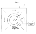
- FIG. 1 is a diagram schematically illustrating a magnetic encoder including a magnetic sensor according to a first embodiment of the present invention.
- a magnetic encoder 1 includes a rotating body 2, a magnetic sensor 3, and an encoder circuit 4.
- Fig. 1 will be described assuming that a rotating magnet 8 rotates in a direction (arrow A direction) opposite to a clockwise direction.
- arrows indicated by dotted lines in Fig. 1 indicate the directions of the magnetic field of the rotating magnet 8.
- the rotating body 2 is provided on a base 5, and the rotation axis 6 of the rotating body 2 is rotatably supported by a bearing (the illustration thereof is omitted) fixed on the base 5.
- the base 5, the bearing, and the rotation axis 6 are formed using nonmagnetic material such as synthetic resin material or the like.
- the rotating body 2 is formed in a thin disk shape and fixed to the rotation axis 6, and includes an inner circumference portion 7 formed using nonmagnetic material and a rotating magnet 8 provided in the outer circumference of the inner circumference portion 7.
- magnetic poles adjacent to each other in a circumferential direction are magnetized with the polarities thereof being different from each other.
- the rotating magnet 8 includes a rotating magnet including four poles whose magnetization pitches are equal to one another.
- the magnetic sensor 3 is fixedly set up so as to be adjacent to the outer circumference surface.
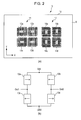
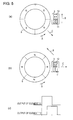
- Fig. 2 is a diagram illustrating the configuration of the magnetic sensor 3
- Fig. 2(a) is a plan pattern diagram illustrating the disposition relationship of the magnetic sensor
- Fig. 2(b) is a magnetic detection bridge circuit diagram in Fig. 2(a) .
- a plurality of magnetic detector elements 11 and 12 (two in the present embodiment) having a same film configuration are mounted on a substrate 9 so as to be adjacent to each other, and these magnetic detector elements 11 and 12 are accommodated within a single sensor package 10.
- a magnetoresistance effect element such as a GMR (Giant Magneto Resistive) element, a TMR (Tunnel Magneto Resistance) element, or the like, which has a high output and a high sensitivity characteristic.
- the magnetic detector element 11 includes a bridge circuit in which four magnetoresistance effect elements 13a to 13d are bridge-connected.
- Each magnetoresistance effect element 13 is formed in a shape (meander shape) in which a plurality of belt-like elongated patterns (stripes), disposed so that the longitudinal directions thereof are parallel to one another, are folded.
- a sensitivity axis direction is a direction (stripe width direction) (an X direction illustrated in Fig. 2(a) ) perpendicular to the longitudinal direction (stripe longitudinal direction) of the elongated pattern.
- the magnetic detector element 12 includes a bridge circuit in which four magnetoresistance effect elements 14a to 14d are bridge-connected.
- Each magnetoresistance effect element 14 is formed in a shape (meander shape) in which a plurality of belt-like elongated patterns (stripes), disposed so that the longitudinal directions thereof are parallel to one another, are folded.
- a sensitivity axis direction is a direction (stripe width direction) (a Y direction illustrated in Fig. 2(a) ) perpendicular to the longitudinal direction (stripe longitudinal direction) of the elongated pattern.
- a magnetic detection bridge circuit will be described. While here a magnetic detection bridge circuit in the magnetic detector element 11 will be cited as an example and described, the magnetic detector element 12 also has the same circuit configuration.
- a power source Vdd is connected to a connection point between the magnetoresistance effect element 13a and the magnetoresistance effect element 13b, and a ground (GND) is connected to a connection point between the magnetoresistance effect element 13c and the magnetoresistance effect element 13d.
- an output Outl is extracted from a connection point between the magnetoresistance effect element 13a and the magnetoresistance effect element 13c, and another output Out2 is extracted from a connection point between the magnetoresistance effect element 13b and the magnetoresistance effect element 13d.
- the two magnetic detector elements 11 and 12 configured in this way are disposed with the sensitivity axis directions of the individual magnetic detector elements 11 and 12 being different (shifted) from each other so that the phases of output signals output from the individual magnetic detector elements 11 and 12 have a desired phase relationship with each other.
- the magnetic detector elements 11 and 12 are disposed so that the sensitivity axis direction of the magnetic detector element 12 is perpendicular to the sensitivity axis direction of the magnetic detector element 11 in a same plane. Accordingly, it is possible to obtain the output signals of the individual magnetic detector elements 11 and 12 having a desired phase relationship with each other. In the present embodiment, it is possible to obtain output signals out of phase with each other by 90 degrees in the phase relationship between the output signals of the individual magnetic detector elements 11 and 12.
- the sensitivity axis directions of the two magnetic detector elements 11 and 12 are disposed so as to be perpendicular to each other, the phase relationship is not limited to this configuration.
- the sensitivity axis directions of three magnetic detector elements may be disposed so as to be shifted from each other by 30 degrees, and it may be possible to obtain output signals out of phase with each other by 30 degrees in the phase relationship between the output signals of the individual magnetic detector elements.
- the encoder circuit 4 detects the rotation of the rotating magnet 8. Specifically, the encoder circuit 4 acquires an output signal from the magnetic detector element 11 subjected to the influence of the flow of a magnetizing field (the direction of the magnetic field) associated with the rotation of the rotating magnet 8, and next acquires an output signal, out of phase with the former output signal by 90 degrees, from the magnetic detector element 12 subjected to the influence of the flow of a magnetizing field (the direction of the magnetic field). In addition, from these two output signals having a phase difference of 90 degrees, the encoder circuit 4 detects the rotation of the rotating magnet 8.
- Fig. 3(a) The film configuration of the magnetoresistance effect element used in the present invention is illustrated in Fig. 3(a) , for example. Namely, as illustrated in Fig. 3(a) , the magnetoresistance effect element has a laminated structure provided in a substrate 21. In addition, in Fig. 3(a) , for ease of explanation, a foundation layer and the like other than the magnetoresistance effect element are omitted in the substrate 21, and illustration is performed.
- the magnetic detector element includes a seed layer 22a, a first ferromagnetic film 23a, an antiparallel coupling film 24a, a second ferromagnetic film 25a, a nonmagnetic intermediate film 26a, soft magnetic free layers (free magnetic layers) 27a and 28a, and a protective layer 29a.
- the seed layer 22a is formed using NiFeCr, Cr, or the like.
- the protective layer 20 is formed using Ta or the like.
- a foundation layer formed, for example, using nonmagnetic material such as at least one element of Ta, Hf, Nb, Zr, Ti, Mo, and W, or the like, may be provided between the substrate 21 and the seed layer 22a.
- the first ferromagnetic film 23a and the second ferromagnetic film 25a are antiferromagnetically coupled to each other through the antiparallel coupling film 24a, and a so-called self-pinned-type ferromagnetic fixed layer (SFP: Synthetic Ferri Pinned layer) is configured.
- SFP Synthetic Ferri Pinned layer
- the thickness of the antiparallel coupling film 24a is set to 0.3 nm to 0.45 nm, or 0.75 nm to 0.95 nm, and hence it is possible to cause a strong antiferromagnetic coupling to occur between the first ferromagnetic film 23a and the second ferromagnetic film 25a.
- the first ferromagnetic film 23a is formed using CoFe alloy including Fe of 40 atomic% to 80 atomic%. This is because the CoFe alloy in this composition range has a large coercive force and it is possible to stably maintain magnetization against an external magnetizing field.
- the second ferromagnetic film 25a is formed using CoFe alloy including Fe of 0 atomic% to 40 atomic%. This is because the CoFe alloy in this composition range has a small coercive force and is easily magnetized in a direction antiparallel to (direction different by 180 degrees from) a direction in which the first ferromagnetic film 23a is preferentially magnetized. As a result, it is possible to further enlarge Hk.
- the second ferromagnetic film 25a by limiting the second ferromagnetic film 25a to this composition range, it is possible to enlarge the resistance change rate of the magnetoresistance effect element.
- the both films 23a and 25a turn out to be magnetized antiparallel to the stripe width direction.
- the magnetization directions of the first ferromagnetic film 23a and the second ferromagnetic film 25a are determined on the basis of the application direction of a magnetizing field at the time of the film formation of the first ferromagnetic film 23a, it is possible to form a plurality of magnetoresistance effect elements having different ferromagnetic fixed layers whose magnetization directions are different from one another, on a same substrate, by changing the application direction of a magnetizing field at the time of the film formation of the first ferromagnetic film 23a.
- the antiparallel coupling film 24a in a ferromagnetic fixed layer is formed using Ru or the like.
- the soft magnetic free layers (free layers) 27a and 28a are formed using magnetic material such as CoFe alloy, NiFe alloy, CoFeNi alloy, or the like.
- the nonmagnetic intermediate layer 26a is formed using Cu or the like.
- the magnetoresistance effect element resistance linearly changes with respect to an external magnetizing field (magnetizing field from a current to be measured) in the stripe width direction, and it is possible to reduce hysteresis.
- a spin-valve configuration is adopted.
- the film configuration of the magnetoresistance effect element used in the magnetic balance current sensor of the present invention there are NiFeCr (the seed layer: 5 nm)/70 FeCo (the first ferromagnetic film: 1.65 nm)/Ru (the antiparallel coupling film: 0.4 nm)/90 CoFe (the second ferromagnetic film: 2 nm)/Cu (the nonmagnetic intermediate layer: 2.2 nm)/90 CoFe (the soft magnetic free layer: 1 nm)/NiFe (the soft magnetic free layer: 7 nm)/Ta (the protective layer: 5 nm).
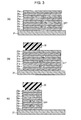
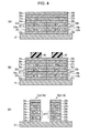
- Figs. 3(a) to 3(c) and Figs. 4(a) to 4(c) are diagrams for explaining a manufacturing method for a magnetoresistance effect element in a current sensor according to the embodiment of the present invention.
- a case in which the magnetoresistance effect element 13 is manufactured will be cited as an example and described.
- the seed layer 22a, the first ferromagnetic film 23a, the antiparallel coupling film 24a, the second ferromagnetic film 25a, the nonmagnetic intermediate film 26a, the soft magnetic free layers (free magnetic layers) 27a and 28a, and the protective layer 29a are sequentially formed.
- a magnetizing field is applied in the stripe width direction of the meander shape.
- the applied-magnetizing field direction is a direction headed from the far side of the plane of paper to the near side thereof
- the applied-magnetizing field direction is a direction headed from the near side of the plane of paper to the far side thereof.
- a magnetizing field is applied in the stripe longitudinal direction of the meander shape.
- a resist layer 30 is formed on the protective layer 29a, and owing to photolithography and etching, the resist layer 30 is caused to remain on a region on the magnetoresistance effect element 13a (13b) side.
- a resist layer 30 is formed on the protective layer 29a, and owing to photolithography and etching, the resist layer 30 is caused to remain on a region on the magnetoresistance effect element 13a (13b) side.
- Fig. 3(c) owing to ion milling or the like, an exposed laminated film is removed, and the substrate 21 in a region in which the magnetoresistance effect element 13c (13d) is to be provided is caused to be exposed.
- a seed layer 22b on the exposed substrate 21, a seed layer 22b, a first ferromagnetic film 23b, an antiparallel coupling film 24b, a second ferromagnetic film 25b, a nonmagnetic intermediate film 26b, soft magnetic free layers (free magnetic layers) 27b and 28b, and a protective layer 29b are sequentially formed.
- a magnetizing field is applied in the stripe width direction of the meander shape.
- the applied-magnetizing field direction is a direction headed from the near side of the plane of paper to the far side thereof
- the applied-magnetizing field direction is a direction headed from the far side of the plane of paper to the near side thereof.
- a magnetizing field is applied in the stripe longitudinal direction of the meander shape.
- the resist layer 30 is formed on the protective layers 29a and 29b, and owing to photolithography and etching, the resist layer 30 is caused to remain on the forming regions of the magnetoresistance effect elements 13a and 13c.
- the resist layer 30 is caused to remain on the forming regions of the magnetoresistance effect elements 13a and 13c.
- Fig. 4(c) owing to ion milling or the like, an exposed laminated film is removed, and the magnetoresistance effect elements 13a and 13c are formed.
- the processing illustrated in Fig. 3 and Fig. 4 is repeated in the same way, and the magnetoresistance effect elements 13b and 13d are formed.
- FIG. 5 is a pattern diagram for explaining the effect of the magnetic encoder 1 according to the present embodiment.
- Figs. 5(a) and 5(b) illustrate a relationship between the direction of the magnetic field of the rotating magnet 8 and the sensitivity axis directions of the magnetic detector elements 11 and 12, and
- Fig. 5(c) illustrates a phase relationship between the output signals of the magnetic detector elements 11 and 12 in Figs. 5(a) and 5(b) . While, in Fig.
- the magnetic sensor 3 is disposed so that the sensitivity axis direction of the magnetic detector element 11 corresponds to the up-and-down direction of the plane of paper and the sensitivity axis direction of the magnetic detector element 12 corresponds to the crosswise direction of the plane of paper, the magnetic sensor 3 is not limited to this configuration.
- the magnetic detector element 11 having the sensitivity axis direction in the same direction as the direction (arrow B direction) of a magnetic field is most strongly subjected to the influence of the magnetizing field with this rotation, and the angle (magnetizing field angle) of the magnetization direction of the free magnetic layer with respect to the magnetization direction of the ferromagnetic fixed layer changes.
- an electrical resistance value changes, and an output signal based on the electrical resistance value according to this change is output to the encoder circuit 4 ( Fig. 5(c) ).
- the rotating magnet 8 has rotated by 45 degrees from the position in Fig.
- the magnetic detector element 12 having the sensitivity axis direction perpendicular to the sensitivity axis direction of the magnetic detector element 11 is most strongly subjected to the influence of the magnetizing field flowing in the direction (arrow C direction) of the magnetic field, and the magnetizing field angle of the magnetization direction of the free magnetic layer with respect to the magnetization direction of the ferromagnetic fixed layer changes.
- an electrical resistance value changes, and an output signal based on the electrical resistance value according to this change is output to the encoder circuit 4 ( Fig. 5(c) ).
- the output signals from the individual magnetic detector elements 11 and 12 are put into a state in which the output signals are out of phase with each other by 90 degrees. Namely, owing to the Sin wave and Cos wave outputs of the magnetic detector elements 11 and 12, a two-phase output with a 90-degree phase difference and a Duty ratio of 50% is obtained.
- the rotation direction of the rotating magnet 8 is detected. Namely, as illustrated in Fig.
- the two magnetic detector elements 11 and 12 are disposed on the same substrate 9 so that the sensitivity axis directions thereof are caused to be perpendicular to each other in response to the phase difference of 90 degrees between the desired output signals. Therefore, even if the magnetic detector elements 11 and 12 are accommodated within the single sensor package 10, it is possible to obtain the output signals of the individual magnetic detector elements 11 and 12 having the desired phase difference, and hence it is possible to downsize the magnetic encoder 1.
- the sensitivity axis directions of the individual magnetic detector elements 11 and 12 are disposed with being different (shifted) from each other so that the phases of the individual output signals have a desired phase relationship with each other. Therefore, even if the two (plural) magnetic detector elements 11 and 12 are accommodated within the single sensor package 10, it is possible to obtain the output signals of the individual magnetic detector elements 11 and 12 having the desired phase relationship with each other without increasing the size of the sensor package 10, and hence it is possible to detect the rotation of the rotating magnet 8 with accuracy. Namely, from the output signal from the magnetic detector element 11 and the output signal from the magnetic detector element 12 out of phase with the output signal of the magnetic detector element 11 by a predetermined phase, it is possible to detect the rotation direction of the rotating magnet 8 with accuracy.
- a magnetic encoder according to the second embodiment of the present invention is different only in the configuration of a magnetic sensor. Accordingly, in particular, the difference will be only described, a same symbol will be used with respect to a same configuration, and the repetitive description will be omitted.
- FIG. 6 is a diagram schematically illustrating the magnetic encoder including the magnetic sensor according to the second embodiment of the present invention.
- a magnetic encoder 41 illustrated in Fig. 6 includes a rotating body 42, a magnetic sensor 43, and an encoder circuit 44.
- the rotating magnet 44 configuring the rotating body 42 magnetic poles adjacent to each other in a circumferential direction are magnetized with the polarities thereof being different from each other, and the rotating magnet 44 includes a rotating magnet including twelve poles whose magnetization pitches are equal to one another.
- the rotating magnet 44 rotates in an anticlockwise direction (arrow A direction) and arrows indicated by dotted lines indicate the directions of the magnetic field of the rotating magnet 44.
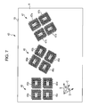
- Fig. 7 is a plan pattern diagram illustrating the disposition relationship of the magnetic sensor 43.
- a plurality of (three in the present embodiment) magnetic detector elements 45, 46, and 47 having a same film configuration are mounted on the substrate 9 so as to be adjacent to each other, and these magnetic detector elements 45, 46, and 47 are accommodated within the single sensor package 10 in a state in which the sensitivity axis directions of the individual magnetic detector elements are shifted from each other by 30 degrees.
- the magnetic detector elements 45, 46, and 47 it is desirable to use a magnetoresistance effect element such as the GMR element, the TMR element, or the like, which has a high output and a high sensitivity characteristic.
- the magnetic detector element 45 includes a bridge circuit in which four magnetoresistance effect elements 45a to 45d are bridge-connected.
- the magnetic detector element 46 includes a bridge circuit in which four magnetoresistance effect elements 46a to 46d are bridge-connected
- the magnetic detector element 47 includes a bridge circuit in which four magnetoresistance effect elements 47a to 47d are bridge-connected.
- Each of the magnetoresistance effect elements 45, 46, and 47 is formed in a shape (meander shape) in which a plurality of belt-like elongated patterns (stripes), disposed so that the longitudinal directions thereof are parallel to one another, are folded.
- a sensitivity axis direction is a direction (stripe width direction) perpendicular to the longitudinal direction (stripe longitudinal direction) of the elongated pattern.
- each of the magnetoresistance effect elements 45, 46, and 47 may include the magnetic detection bridge circuit illustrated in Fig. 2(b) .
- the three magnetic detector elements 45, 46, and 47 configured in this way are disposed with the sensitivity axis directions of the individual magnetic detector elements 45, 46, and 47 being different (shifted) from each other so that the phases of the output signals output from the individual magnetic detector elements 45, 46, and 47 have a desired phase relationship with each other.
- the sensitivity axis direction (arrow C direction) of the magnetic detector element 46 is disposed so as to be shifted by 30 degrees in one direction (the illustrated direction corresponds to an anticlockwise direction) in a same plane with respect to the sensitivity axis direction (arrow B direction) of the magnetic detector element 45, and the sensitivity axis direction (arrow D direction) of the magnetic detector element 47 is disposed so as to be shifted by 30 degrees in the same direction in a same plane with respect to the sensitivity axis direction (arrow C direction) of the magnetic detector element 46 (namely, shifted by 60 degrees in the same direction with respect to the sensitivity axis direction of the magnetic detector element 45).
- the encoder circuit 4 detects the rotation of the rotating magnet 44. Specifically, the encoder circuit 4 acquires an output signal from the magnetic detector element 45 most strongly subjected to the influence of the flow of a magnetizing field (the direction of the magnetic field) associated with the rotation of the rotating magnet 44, and next acquires an output signal, out of phase with the phase of the former output signal (the output signal output from the magnetic detector element 45) by 30 degrees, from the magnetic detector element 46 most strongly subjected to the influence of the flow of a magnetizing field with the rotation of the rotating magnet 44.
- a magnetizing field the direction of the magnetic field
- the encoder circuit 4 acquires an output signal, out of phase with the phase of the former output signal (the output signal output from the magnetic detector element 46) by 30 degrees, from the magnetic detector element 47 subjected to the influence of the flow of a magnetizing field with the rotation of the rotating magnet 44. In addition, from these three output signals having a phase difference of 30 degrees, the encoder circuit 4 detects the rotation of the rotating magnet 44.
- a seed layer 52a on a substrate 51, a seed layer 52a, a first ferromagnetic film 53a, an antiparallel coupling film 54a, a second ferromagnetic film 55a, a nonmagnetic intermediate layer 56a, soft magnetic free layers (free magnetic layers) 57a and 58a, and a protective layer 59a are sequentially formed.
- a magnetizing field is applied in the stripe width direction of the meander shape.
- the applied-magnetizing field direction of the first ferromagnetic film 53a is a direction headed from the far side of the plane of paper to the near side thereof
- the applied-magnetizing field direction of the second ferromagnetic film 55a is a direction headed from the near side of the plane of paper to the far side thereof.
- a magnetizing field is applied in the stripe longitudinal direction of the meander shape.
- a resist layer 60 is formed on the protective layer 59a, and owing to photolithography and etching, the resist layer 60 is caused to remain on a region on the magnetoresistance effect element 45a (45b) side.
- a resist layer 60 is formed on the protective layer 59a, and owing to photolithography and etching, the resist layer 60 is caused to remain on a region on the magnetoresistance effect element 45a (45b) side.
- Fig. 8(c) owing to ion milling or the like, an exposed laminated film is removed, and the substrate 51 in a region in which the magnetoresistance effect element 45c (45d) is to be provided is caused to be exposed.
- a seed layer 52b, a first ferromagnetic film 53b, an antiparallel coupling film 54b, a second ferromagnetic film 55b, a nonmagnetic intermediate film 56b, soft magnetic free layers (free magnetic layers) 57b and 58b, and a protective layer 59b are sequentially formed.
- a magnetizing field is applied in the stripe width direction of the meander shape.
- the applied-magnetizing field direction of the first ferromagnetic film 53b is a direction headed from the near side of the plane of paper to the far side thereof
- the applied-magnetizing field direction of the second ferromagnetic film 55b is a direction headed from the far side of the plane of paper to the near side thereof.
- a magnetizing field is applied in the stripe longitudinal direction of the meander shape.
- the resist layer 60 is formed on the protective layers 59a and 59b, and owing to photolithography and etching, the resist layer 60 is caused to remain on the forming regions of the magnetoresistance effect elements 45a and 45c.
- the resist layer 60 is caused to remain on the forming regions of the magnetoresistance effect elements 45a and 45c.
- Fig. 8(f) owing to ion milling or the like, an exposed laminated film is removed, and the magnetoresistance effect elements 45a and 45c are formed.
- the above-mentioned processing is repeated in the same way, and the magnetoresistance effect elements 45b and 45d are formed.
- a seed layer 62a, a first ferromagnetic film 63a, an antiparallel coupling film 64a, a second ferromagnetic film 65a, a nonmagnetic intermediate layer 66a, soft magnetic free layers (free magnetic layers) 67a and 68a, and a protective layer 69a are sequentially formed ( Fig. 9(a) ).
- a magnetizing field is applied in the stripe width direction of the meander shape.
- the applied-magnetizing field direction of the first ferromagnetic film 63a is a direction out of phase by 30 degrees with the applied-magnetizing field direction of the first ferromagnetic film 53a in the magnetoresistance effect element 45a
- the applied-magnetizing field direction of the second ferromagnetic film 65a is a direction out of phase by 30 degrees with the applied-magnetizing field direction of the second ferromagnetic film 55a in the magnetoresistance effect element 45a.
- a magnetizing field is applied in the stripe longitudinal direction of the meander shape.
- the resist layer 60 is formed on the protective layer 69a, and owing to photolithography and etching, the resist layer 60 is caused to remain on a region on the magnetic detector element 46a (46b) side.
- an exposed laminated film is removed, and the substrate 51 in a region in which the magnetoresistance effect element 46c (46d) is to be provided is caused to be exposed.
- a seed layer 62b, a first ferromagnetic film 63b, an antiparallel coupling film 64b, a second ferromagnetic film 65b, a nonmagnetic intermediate film 66b, soft magnetic free layers (free magnetic layers) 67b and 68b, and a protective layer 69b are sequentially formed ( Fig. 9(a) ).
- a magnetizing field is applied in the stripe width direction of the meander shape.
- the applied-magnetizing field direction of the first ferromagnetic film 63b is a direction out of phase by 30 degrees with the applied-magnetizing field direction of the first ferromagnetic film 53b in the magnetoresistance effect element 45c
- the applied-magnetizing field direction of the second ferromagnetic film 65b is a direction out of phase by 30 degrees with the applied-magnetizing field direction of the second ferromagnetic film 55b in the magnetoresistance effect element 45c.
- a magnetizing field is applied in the stripe longitudinal direction of the meander shape.
- the resist layer 60 is formed on the protective layers 69a and 69b, and owing to photolithography and etching, the resist layer 60 is caused to remain on the forming regions of the magnetoresistance effect elements 46a and 46c.
- the resist layer 60 is caused to remain on the forming regions of the magnetoresistance effect elements 46a and 46c.
- Fig. 9(c) owing to ion milling or the like, an exposed laminated film is removed, and the magnetoresistance effect elements 46a and 46c are formed.
- the above-mentioned processing is repeated in the same way, and the magnetoresistance effect elements 46b and 46d are formed.
- a seed layer 72a, a first ferromagnetic film 73a, an antiparallel coupling film 74a, a second ferromagnetic film 75a, a nonmagnetic intermediate layer 76a, soft magnetic free layers (free magnetic layers) 77a and 78a, and a protective layer 79a are sequentially formed ( Fig. 10(a) ).
- a magnetizing field is applied in the stripe width direction of the meander shape.
- the applied-magnetizing field direction of the first ferromagnetic film 73a is a direction out of phase by 30 degrees with the applied-magnetizing field direction of the first ferromagnetic film 63a in the magnetoresistance effect element 46a
- the applied-magnetizing field direction of the second ferromagnetic film 75a is a direction out of phase by 30 degrees with the applied-magnetizing field direction of the second ferromagnetic film 65a in the magnetoresistance effect element 46a.
- a magnetizing field is applied in the stripe longitudinal direction of the meander shape.
- the resist layer 60 is formed on the protective layer 79a, and owing to photolithography and etching, the resist layer 60 is caused to remain on a region on the magnetic detector element 47a (47b) side.
- an exposed laminated film is removed, and the substrate 51 in a region in which the magnetoresistance effect element 47c (47d) is to be provided is caused to be exposed.
- a seed layer 72b, a first ferromagnetic film 73b, an antiparallel coupling film 74b, a second ferromagnetic film 75b, a nonmagnetic intermediate film 76b, soft magnetic free layers (free magnetic layers) 77b and 78b, and a protective layer 79b are sequentially formed ( Fig. 10(a) ).
- a magnetizing field is applied in the stripe width direction of the meander shape.
- the applied-magnetizing field direction of the first ferromagnetic film 73b is a direction out of phase by 30 degrees with the applied-magnetizing field direction of the first ferromagnetic film 63b in the magnetoresistance effect element 46c
- the applied-magnetizing field direction of the second ferromagnetic film 75b is a direction out of phase by 30 degrees with the applied-magnetizing field direction of the second ferromagnetic film 65b in the magnetoresistance effect element 46c.
- a magnetizing field is applied in the stripe longitudinal direction of the meander shape.
- the resist layer 60 is formed on the protective layers 79a and 79b, and owing to photolithography and etching, the resist layer 60 is caused to remain on the forming regions of the magnetoresistance effect elements 47a and 47c.
- the resist layer 60 is caused to remain on the forming regions of the magnetoresistance effect elements 47a and 47c.
- Fig. 10(c) owing to ion milling or the like, an exposed laminated film is removed, and the magnetoresistance effect elements 47a and 47c are formed.
- the above-mentioned processing is repeated in the same way, and the magnetoresistance effect elements 47b and 47d are formed.
- the individual magnetic detector elements 45, 46, and 47 are manufactured in a state in which the sensitivity axis directions thereof are shifted from each other by 30 degrees.
- the sensitivity axis direction of the magnetic detector element 45 is formed so as to be a direction shifted from the sensitivity axis direction of the magnetic detector element 45 by 30 degrees
- the sensitivity axis direction of the magnetic detector element 47 is formed so as to be a direction (direction shifted from the sensitivity axis direction of the magnetic detector element 45 by 60 degrees in a same direction) further shifted from the sensitivity axis direction of the magnetic detector element 46 by 30 degrees in the same direction ( Fig. 10(c) ).
- FIG. 11 is a pattern diagram for explaining the effect of the magnetic encoder 41 according to the present embodiment.
- Figs. 11(a), 11(b), and 11(c) illustrate a relationship between the direction of the magnetic field of the rotating magnet 44 and the sensitivity axis directions of the individual magnetic detector elements 45, 46, and 47
- Fig. 11(d) illustrates output signals output from the magnetic detector elements 45, 46, and 47 in Figs. 11(a), 11(b), and 11(c) .
- the magnetic sensor 43 will be cited as an example and described where, with reference to the sensitivity axis direction (the crosswise direction of the plane of paper) of the magnetic detector element 45 nearest to the rotating magnet 44, the sensitivity axis direction of the magnetic detector element 46 is disposed so as to be shifted from the sensitivity axis direction of the magnetic detector element 45 by 30 degrees in an anticlockwise fashion and the sensitivity axis direction of the magnetic detector element 47 is disposed so as to be shifted from the sensitivity axis direction of the magnetic detector element 46 by 30 degrees in an anticlockwise fashion.
- the magnetic sensor 43 is not limited to this disposition position and this disposition configuration of the magnetic sensor 43 (the magnetic detector elements 45, 46, and 47).
- the magnetic detector element 45 having the sensitivity axis direction in approximately the same direction as the direction of a magnetic field is most strongly subjected to the influence of the magnetizing field, and the angle (magnetizing field angle) of the magnetization direction of the free magnetic layer with respect to the magnetization direction of the ferromagnetic fixed layer changes.
- an electrical resistance value changes, and an output signal based on the electrical resistance value according to this change is output to the encoder circuit 4 ( Fig. 11(d) ).
- the magnetic detector element 46 having the sensitivity axis direction out of phase with the sensitivity axis direction of the magnetic detector element 45 by 30 degrees is most strongly subjected to the influence of the magnetizing field flowing in the direction of the magnetic field, and the magnetizing field angle of the magnetization direction of the free magnetic layer with respect to the magnetization direction of the ferromagnetic fixed layer changes ( Fig. 11(b) ).
- an electrical resistance value changes, and an output signal based on the electrical resistance value according to this change is output to the encoder circuit 4 ( Fig. 11(d) ).
- an output signal output from the magnetic detector element 46 is put into a state in which the output signal is out of phase with an output signal output from the magnetic detector element 45 by 30 degrees.
- the magnetic detector element 47 having the sensitivity axis direction out of phase with the sensitivity axis direction of the magnetic detector element 46 by 30 degrees is most strongly subjected to the influence of the magnetizing field flowing in the direction of the magnetic field, and the magnetizing field angle of the magnetization direction of the free magnetic layer with respect to the magnetization direction of the ferromagnetic fixed layer changes ( Fig. 11(c) ).
- an electrical resistance value changes, and an output signal based on the electrical resistance value according to this change is output to the encoder circuit 4 ( Fig. 11(d) ).
- an output signal output from the magnetic detector element 47 is put into a state in which the output signal is out of phase with the output signal output from the magnetic detector element 46 by 30 degrees.
- a three-phase output signal having a 30-degree phase difference between the magnetic detector elements 45, 46, and 47 In the encoder circuit 4, from the phase relationship of the output signal of the magnetic detector element 46, out of phase with the phase of the output signal from the magnetic detector element 45 by 30 degrees, the rotation direction of the rotating magnet 44 is detected, and from the phase relationship of the output signal of the magnetic detector element 47, out of phase with the phase of the output signal from the magnetic detector element 46 by 30 degrees, the rotation direction of the rotating magnet 44 is detected.
- the sensitivity axis directions of the individual magnetic detector elements 45, 46, and 47 are disposed with being different (shifted) from each other by 30 degrees in the same direction so that the phases of the individual output signals have a desired phase relationship with each other. Therefore, even if the plural magnetic detector elements 45, 46, and 47 are accommodated within the single sensor package 10, it is possible to obtain the output signals of the individual magnetic detector elements 45, 46, and 47 having the desired phase relationship with each other without increasing the size of the sensor package 10, and hence it is possible to detect the rotation of the rotating magnet 44 with accuracy.
- the output signal of the magnetic detector element 46 having a predetermined phase shift with respect to the output signal of the magnetic detector element 45, and the output signal of the magnetic detector element 47 having a predetermined phase shift with respect to the output signal of the magnetic detector element 46 it is possible to detect the rotation direction and the angular phase of the rotating magnet 44 with accuracy.
- the sensitivity axis directions of the magnetic detector elements 45, 46, and 47 are disposed so as to be shifted from each other by 30 degrees.
- the magnetic detector elements 45, 46, and 47 are disposed so the sensitivity axis directions of the three magnetic detector elements 45, 46, and 47 are shifted from each other by 60 degrees or 120 degrees, it is possible to obtain a three-phase output signal having the phase difference of 60 degrees or 120 degrees.
- the magnetic sensor 43 configured in this way to the rotation control of a brushless motor used for a drive motor for a vehicle such as an electric vehicle, a hybrid vehicle, or the like or an electronic device or the like, for example.
- a brushless motor used for a drive motor for a vehicle such as an electric vehicle, a hybrid vehicle, or the like or an electronic device or the like, for example.
- three pairs of coils, out of phase with each other, for example, by 120 degrees, are disposed with respect to the magnetic pole of a rotating magnet, it is controlled with which polarity a current is supplied to each coil in response to the rotational position of the rotating magnet, and the rotating magnet is controlled so as to rotate with maximum attraction and maximum repulsion occurring.
- a magnetic sensor with a three-phase output is used.
- Fig. 12 is a pattern diagram illustrating an example of a brushless motor into which a magnetic sensor is applied.
- Fig. 12(a) illustrates a brushless motor into which a magnetic sensor according to the present embodiment is applied
- Fig. 12(b) illustrates a brushless motor into which a magnetic sensor according to a comparative example is applied.
- a magnetic sensor 43 according to the present embodiment is a magnetic sensor where the three magnetic detector elements 45, 46, and 47 whose sensitivity axis directions are shifted by 60 degrees from each other in a same direction are accommodated within the single sensor package 10.
- the magnetic sensor according to the comparative example is a magnetic sensor where a single magnetic detector element is accommodated within a single sensor package and the three magnetic sensors S are used.
- a brushless motor 30 includes a rotatable rotor magnet 31 and a stator 32 provided in the outer circumference of the rotor magnet 31.
- a plurality of coils 33 are attached to the stator 32 at regular intervals in a circumferential direction (6 coils 33 are attached at intervals of 60 degrees) so as to face the outer circumference surface of the rotor magnet 31.
- a north pole and a south pole are alternately magnetized with an equal pitch in a radial direction, and a north pole and a south pole are alternately magnetized with an equal pitch along a rotation direction.
- a first magnetic sensor S1 is provided between predetermined coils 33a and 33b with being adjacent to the outer circumference of the rotor magnet 31.
- a second magnetic sensor S2 is provided, with being adjacent to the outer circumference of the rotor magnet 31, between coils 33b and 33c adjacent to the coils 33a and 33b between which the first magnetic sensor S1 is fixedly set up, so that the sensitivity axis direction of the magnetic sensor S2 is shifted by 60 degrees with respect to the sensitivity axis direction of the first magnetic sensor S1.
- a third magnetic sensor S3 is provided, with being adjacent to the outer circumference of the rotor magnet 31, between coils 33c and 33d adjacent to the coils 33b and 33c between which the second magnetic sensor S2 is fixedly set up, so that the sensitivity axis direction of the magnetic sensor S3 is shifted by 60 degrees with respect to the sensitivity axis direction of the second magnetic sensor S2.
- the sensitivity axis directions of the remaining two magnetic sensors S2 and S3 it is necessary for the sensitivity axis directions of the remaining two magnetic sensors S2 and S3 to be individually shifted by 60 degrees from the sensitivity axis direction of the magnetic sensor S1 used as a reference, and it is necessary for the three magnetic sensors S1, S2, and S3 to be individually mounted with accuracy. Accordingly, when the mounting accuracy of the magnetic sensors S1, S2, and S3 vary, this variation influences an output signal from each of the magnetic sensors S1, S2, and S3, and there is a possibility that it is not possible to obtain a signal having a desired phase difference.
- the magnetic sensor 43 according to the present embodiment illustrated in Fig. 12(a) since the magnetic sensor 43 has been accommodated within the single sensor package 10 in a state in which the sensitivity axis directions are shifted from each other by 60 degrees, it is only necessary to fixedly set up the magnetic sensor 43 between the two coils 33b and 33c so as to be adjacent to the outer circumference of the rotor magnet 31. Accordingly, in the case of the magnetic sensor 43 according to the present embodiment, it is possible to obtain a 3-phase output signal (A phase, B phase, and C phase outputs) having the phase difference of 60 degrees from the individual magnetic detector elements 45, 46, and 47 in the magnetic sensor 43 without being influenced by the mounting accuracy of the magnetic sensor 43 ( Fig. 13 ).
- the magnetic sensor 43 according to the present embodiment it is possible for the magnetic sensor 43 according to the present embodiment to obtain a signal having a desired phase difference without being influenced by the mounting accuracy of the magnetic sensor.
- it is only necessary to attach the single magnetic sensor 43 it is possible to reduce a process for attaching a magnetic sensor and it is possible to simply attach the magnetic sensor.
- the possibility of an attachment position is improved, and it is possible to reduce the component size of a substrate or the like and commonalize the component shape of the substrate or the like.
- the magnetic sensor 43 has been configured by accommodating, within the single sensor package 10, the three magnetic detector elements 45, 46, and 47 whose sensitivity axis directions are shifted from each other by 60 degrees.
- the magnetic sensor 43 has been disposed so as to be adjacent to the outer circumference portion of the rotating magnet 44 including twelve poles whose magnetization pitches are equal to one another.
- a sintered neodymium magnet has been used in which twelve poles are radial magnetized.
- the magnetic flux density in this magnetic sensor 43 increases with a decrease in a distance (Gap) from the outer circumference of the rotating magnet 44 to the magnetic sensor 43, and a magnetic flux density in each Gap is approximately constant even if the rotor rotational angle changes ( Fig. 14(a) ).
- the magnetizing field vector angle linearly corresponds to the rotor rotational angle in all Gaps ( Fig. 14 (b) ).
- the individual output signals (A phase, B phase, and C phase outputs) output from the magnetic detector elements 45, 46, and 47 are extracted in a state in which the output signals have the phase difference of 60 degrees ( Fig. 15(a) ), and these outputs from the individual magnetic detector elements are converted into ON/OFF digital signals on an IC to be output ( Fig. 15(b) ).
- Fig. 16 it has been possible to obtain the three-phase output having the phase difference of 60 degrees from the individual magnetic detector elements 45, 46, and 47 in the magnetic sensor 43.
- the magnetic sensor according to the comparative example has been configured by accommodating the single magnetic detector element in the single sensor package, and three magnetic sensors configured in this way have been prepared.
- the three magnetic sensors have been disposed with the sensitivity axis directions of the magnetic detector elements in the individual magnetic sensors being shifted from each other by 30 degrees.
- a magnetic sensor according to the present invention has the advantageous effect of being capable of obtaining output signals from a plurality of magnetic detector elements, which have a desired phase relationship with each other, and detecting the rotation of a rotating magnet with accuracy, without the size of a single sensor package being increased, and is useful for the rotation control of a brushless motor used as a drive motor for a vehicle, an electronic device, or the like, for example.
Landscapes
- Physics & Mathematics (AREA)
- General Physics & Mathematics (AREA)
- Transmission And Conversion Of Sensor Element Output (AREA)
- Measurement Of Length, Angles, Or The Like Using Electric Or Magnetic Means (AREA)
- Brushless Motors (AREA)
Abstract
To obtain output signals where the phases of the output signals of two magnetic detector elements have a desired phase relationship with each other, without the size of a single sensor package being increased even if the two magnetic detector elements are accommodated within the sensor package. A magnetic sensor (3) includes two magnetic detector elements (11, 12) provided so as to face the outer circumference portion of a rotating magnet (8) in which magnetic poles adjacent to each other in a circumferential direction are magnetized with the polarities thereof being different from each other, and the two magnetic detector elements (11, 12) are disposed in a single sensor package (10) with the sensitivity axis directions of the two magnetic detector elements (11, 12) being different from each other so that the phases of output signals output from the two magnetic detector elements (11, 12) have a desired phase relationship with each other.
Description
- The present invention relates to a magnetic sensor utilizing a magnetic detector element and a magnetic encoder equipped therewith.
- In the past, as this type of magnetic encoder, there has been a magnetic encoder that detects the rotation direction of a rotating magnet using two magnetic sensors including a single magnetic detector element (refer to PTL 1). In this magnetic encoder, in the rotation direction of the rotating magnet in which a north pole and a south pole are alternately magnetized, two magnetic sensors are disposed so that the output signals of the two magnetic detector elements are out of phase with each other by a predetermined phase. In addition, on the basis of a phase shifts between the output signals of the individual magnetic detector elements, the magnetic encoder detects the rotation direction of the rotating magnet.
- PTL 1: Japanese Unexamined Patent Application Publication No.
2001-201364 - Incidentally, in recent years, a magnetic detector element (GMR element) utilizing a giant magnetoresistance effect (GMR effect) has been used for a magnetic encoder, and there has been a magnetic sensor used for applied detection, which utilizes this magnetic encoder. In addition, the downsizing of a unit accommodating a magnetic sensor or a rotating magnet has been requested, and to accommodate a plurality of magnetic detector elements within a single sensor package has been developed.
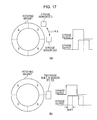
- However, when a phase relationship between two output signals (an A phase output and a B phase output) has been adjusted using a positional relationship between individual magnetic detector elements E1 and E2 (
Fig. 17(a) ) in such a way as in the past and the magnetic detector elements E1 and E2 have been accommodated in the single sensor package, the phase relationship between the output signals of the individual magnetic detector elements E1 and E2 has been shifted (Fig. 17(b) ), and there has occurred a problem that it is hard to detect the rotation direction of the rotating magnet with accuracy. In addition, since there is a constraint on the size or the like of an IC accommodated in the sensor package with the downsizing of the magnetic sensor being requested, there is a limit on adjusting the physical placement of the individual magnetic detector elements E1 and E2 within the sensor package so that the output signals have a desired phase difference therebetween. - In view of such a regard, the present invention is made, and an object thereof is to provide a magnetic sensor capable of obtaining an output signal where the phases of the output signals of a plurality of magnetic detector elements have a desired phase relationship with one another, without the size of a single sensor package being increased even if the plural magnetic detector elements are accommodated within the sensor package, and a magnetic encoder equipped with the magnetic sensor.
- A magnetic sensor of the present invention is a magnetic sensor including first and second magnetic detector elements provided so as to face an outer circumference portion of a rotating magnet in which magnetic poles adjacent to each other in a circumferential direction are magnetized with polarities thereof being different from each other, wherein the first and second magnetic detector elements are disposed in a single sensor package with sensitivity axis directions of the individual magnetic detector elements being different from each other so that phases of output signals output from the first and second magnetic detector elements have a desired phase relationship with each other.
- According to this configuration, the sensitivity axis directions of the individual magnetic detector elements are disposed with being different (shifted) from each other so that the phases of the individual output signals have a desired phase relationship with each other. Therefore, even if the two magnetic detector elements are accommodated within the single sensor package, it is possible to obtain the output signals of the individual magnetic detector elements having a desired phase relationship with one another without the size of the sensor package being increased.
- In the above-mentioned magnetic sensor, the rotating magnet includes four poles whose magnetization pitches are equal to one another, and a sensitivity axis direction of the other magnetic detector element is caused to be perpendicular to a sensitivity axis direction of one magnetic detector element in a same plane.
- The above-mentioned magnetic sensor includes a third magnetic detector element provided so as to face the outer circumference portion of the rotating magnet, wherein the first, second, and third magnetic detector elements are disposed in the single sensor package with sensitivity axis directions of the individual magnetic detector elements being different from each other so that phases of output signals output from the first, second, and third magnetic detector elements have a desired phase relationship with each other.
- In this case, it is desirable that the first, second, and third magnetic detector elements are disposed so that the sensitivity axis directions of the individual magnetic detector elements are shifted from each other by 30 degrees, 60 degrees, or 120 degrees in a same plane.
- In the above-mentioned magnetic sensor, the first and second magnetic detector elements are magnetoresistance effect elements.
- A magnetic encoder of the present invention includes a rotating magnet in which magnetic poles adjacent to each other in a circumferential direction are magnetized with polarities thereof being different from each other, and a magnetic sensor including first and second magnetic detector elements provided so as to face an outer circumference portion of the rotating magnet, wherein the first and second magnetic detector elements are disposed in a single sensor package with sensitivity axis directions of the individual magnetic detector elements being different from each other so that phases of output signals output from the first and second magnetic detector elements have a desired phase shift.
- According to this configuration, the sensitivity axis directions of the individual magnetic detector elements are disposed with being different (shifted) from each other so that the phases of the individual output signals have a desired phase relationship with each other. Therefore, even if the two magnetic detector elements are accommodated within the single sensor package, it is possible to obtain the output signals of the individual magnetic detector elements having a desired phase relationship with one another and it is possible to detect the rotation direction of the rotating magnet with accuracy, without the size of the sensor package being increased.
- In the above-mentioned magnetic encoder, the magnetic sensor includes a third magnetic detector element provided so as to face the outer circumference portion of the rotating magnet, wherein the first, second, and third magnetic detector elements are disposed in the single sensor package with sensitivity axis directions of the individual magnetic detector elements being different from each other so that phases of output signals output from the first, second, and third magnetic detector elements have a desired phase relationship with each other.
- According to the present invention, even if a plurality of magnetic detector elements are accommodated within a single sensor package, it is possible to obtain an output signal where the phases of the output signals of the plural magnetic detector elements have a desired phase relationship with each other, without the size of the sensor package being increased.
-
- [
Fig. 1] Fig. 1 is a diagram schematically illustrating a magnetic encoder according to a first embodiment of the present invention. - [
Fig. 2] Fig. 2 is a diagram illustrating a configuration of a magnetic sensor according to the present embodiment. - [
Fig. 3] Fig. 3 is a diagram for explaining a manufacturing method for a magnetic detector element according to the present embodiment. - [
Fig. 4] Fig. 4 is a diagram for explaining a manufacturing method for a magnetic detector element according to the present embodiment. - [
Fig. 5] Fig. 5 is a diagram for explaining an effect of a magnetic encoder according to the present embodiment. - [
Fig. 6] Fig. 6 is a diagram schematically illustrating a magnetic encoder according to a second embodiment of the present invention. - [
Fig. 7] Fig. 7 is a diagram illustrating a configuration of a magnetic sensor according to the present embodiment. - [
Fig. 8] Fig. 8 is a diagram for explaining a manufacturing method for a magnetic detector element according to the present embodiment. - [
Fig. 9] Fig. 9 is a diagram for explaining a manufacturing method for a magnetic detector element according to the present embodiment. - [
Fig. 10] Fig. 10 is a diagram for explaining a manufacturing method for a magnetic detector element according to the present embodiment. - [
Fig. 11] Fig. 11 is a diagram for explaining an effect of a magnetic encoder according to the present embodiment. - [
Fig. 12] Fig. 12 is a pattern diagram illustrating examples of brushless motors into which magnetic sensors according to the present embodiment and a comparative example are applied. - [
Fig. 13] Fig. 13 is a diagram illustrating an example of a signal output from a magnetic sensor according to the present embodiment. - [
Fig. 14] Fig. 14(a) is a diagram illustrating a relationship between a magnetic flux density of a magnetic sensor and a rotor rotational angle of a rotating magnet (rotor magnet) according to an embodiment, andFig. 14(b) is a diagram illustrating a relationship between a magnetizing field vector angle of a magnetic sensor and a rotor rotational angle according to an embodiment. - [
Fig. 15] Fig. 15(a) illustrates an output signal from each magnetic detector element in a magnetic sensor according to an embodiment, andFig. 15(b) illustrates a signal into which the signal illustrated inFig. 15(a) is digital-converted. - [
Fig. 16] Fig. 16 is a diagram illustrating an example of an output signal from each magnetic detector element in a magnetic sensor according to an embodiment. - [
Fig. 17] Fig. 17 is a diagram for explaining a problem of the present invention. - Hereinafter, the embodiments of the present invention will be described in detail with reference to accompanying drawings. A magnetic encoder including a magnetic sensor according to the embodiment of the present invention detects the rotation of a rotating magnet serving as a magnetic flux generation source, on the basis of the phase shifts of the sensor outputs of a plurality of magnetic detector elements.
-
Fig. 1 is a diagram schematically illustrating a magnetic encoder including a magnetic sensor according to a first embodiment of the present invention. Amagnetic encoder 1 includes arotating body 2, amagnetic sensor 3, and anencoder circuit 4. In addition,Fig. 1 will be described assuming that a rotatingmagnet 8 rotates in a direction (arrow A direction) opposite to a clockwise direction. In addition, arrows indicated by dotted lines inFig. 1 indicate the directions of the magnetic field of the rotatingmagnet 8. - The rotating
body 2 is provided on abase 5, and the rotation axis 6 of the rotatingbody 2 is rotatably supported by a bearing (the illustration thereof is omitted) fixed on thebase 5. Thebase 5, the bearing, and the rotation axis 6 are formed using nonmagnetic material such as synthetic resin material or the like. The rotatingbody 2 is formed in a thin disk shape and fixed to the rotation axis 6, and includes aninner circumference portion 7 formed using nonmagnetic material and a rotatingmagnet 8 provided in the outer circumference of theinner circumference portion 7. In the rotatingmagnet 8, magnetic poles adjacent to each other in a circumferential direction are magnetized with the polarities thereof being different from each other. In the present embodiment, the rotatingmagnet 8 includes a rotating magnet including four poles whose magnetization pitches are equal to one another. On thebase 5, at a position facing the outer circumference surface of the rotatingmagnet 8, themagnetic sensor 3 is fixedly set up so as to be adjacent to the outer circumference surface. -
Fig. 2 is a diagram illustrating the configuration of themagnetic sensor 3,Fig. 2(a) is a plan pattern diagram illustrating the disposition relationship of the magnetic sensor, andFig. 2(b) is a magnetic detection bridge circuit diagram inFig. 2(a) . As illustrated inFig. 2(a) , in themagnetic sensor 3, a plurality ofmagnetic detector elements 11 and 12 (two in the present embodiment) having a same film configuration are mounted on a substrate 9 so as to be adjacent to each other, and thesemagnetic detector elements single sensor package 10. Here, as themagnetic detector elements - The
magnetic detector element 11 includes a bridge circuit in which fourmagnetoresistance effect elements 13a to 13d are bridge-connected. Each magnetoresistance effect element 13 is formed in a shape (meander shape) in which a plurality of belt-like elongated patterns (stripes), disposed so that the longitudinal directions thereof are parallel to one another, are folded. In each magnetoresistance effect element 13 formed in this meander shape, usually a sensitivity axis direction (Pin direction) is a direction (stripe width direction) (an X direction illustrated inFig. 2(a) ) perpendicular to the longitudinal direction (stripe longitudinal direction) of the elongated pattern. - In the same way, the
magnetic detector element 12 includes a bridge circuit in which fourmagnetoresistance effect elements 14a to 14d are bridge-connected. Each magnetoresistance effect element 14 is formed in a shape (meander shape) in which a plurality of belt-like elongated patterns (stripes), disposed so that the longitudinal directions thereof are parallel to one another, are folded. In each magnetoresistance effect element 14 formed in this meander shape, usually a sensitivity axis direction (Pin direction) is a direction (stripe width direction) (a Y direction illustrated inFig. 2(a) ) perpendicular to the longitudinal direction (stripe longitudinal direction) of the elongated pattern. - Using
Fig. 2(b) , a magnetic detection bridge circuit will be described. While here a magnetic detection bridge circuit in themagnetic detector element 11 will be cited as an example and described, themagnetic detector element 12 also has the same circuit configuration. In the magnetic detection bridge circuit illustrated inFig. 2(b) , a power source Vdd is connected to a connection point between themagnetoresistance effect element 13a and themagnetoresistance effect element 13b, and a ground (GND) is connected to a connection point between themagnetoresistance effect element 13c and themagnetoresistance effect element 13d. Furthermore, in this magnetic field detection bridge circuit, an output Outl is extracted from a connection point between themagnetoresistance effect element 13a and themagnetoresistance effect element 13c, and another output Out2 is extracted from a connection point between themagnetoresistance effect element 13b and themagnetoresistance effect element 13d. - The two
magnetic detector elements magnetic detector elements magnetic detector elements magnetic detector elements magnetic detector element 12 is perpendicular to the sensitivity axis direction of themagnetic detector element 11 in a same plane. Accordingly, it is possible to obtain the output signals of the individualmagnetic detector elements magnetic detector elements magnetic detector elements - On the basis of the phase shift between the output signals of the two
magnetic detector elements encoder circuit 4 detects the rotation of therotating magnet 8. Specifically, theencoder circuit 4 acquires an output signal from themagnetic detector element 11 subjected to the influence of the flow of a magnetizing field (the direction of the magnetic field) associated with the rotation of therotating magnet 8, and next acquires an output signal, out of phase with the former output signal by 90 degrees, from themagnetic detector element 12 subjected to the influence of the flow of a magnetizing field (the direction of the magnetic field). In addition, from these two output signals having a phase difference of 90 degrees, theencoder circuit 4 detects the rotation of therotating magnet 8. - Next, using
Fig. 3 andFig. 4 , the film configuration of the magnetoresistance effect element and the manufacturing method therefor will be described. The film configuration of the magnetoresistance effect element used in the present invention is illustrated inFig. 3(a) , for example. Namely, as illustrated inFig. 3(a) , the magnetoresistance effect element has a laminated structure provided in asubstrate 21. In addition, inFig. 3(a) , for ease of explanation, a foundation layer and the like other than the magnetoresistance effect element are omitted in thesubstrate 21, and illustration is performed. The magnetic detector element includes aseed layer 22a, a firstferromagnetic film 23a, anantiparallel coupling film 24a, a secondferromagnetic film 25a, a nonmagneticintermediate film 26a, soft magnetic free layers (free magnetic layers) 27a and 28a, and aprotective layer 29a. - The
seed layer 22a is formed using NiFeCr, Cr, or the like. Theprotective layer 20 is formed using Ta or the like. In addition, in the above-mentioned laminated structure, a foundation layer formed, for example, using nonmagnetic material such as at least one element of Ta, Hf, Nb, Zr, Ti, Mo, and W, or the like, may be provided between thesubstrate 21 and theseed layer 22a. - In this magnetic detector element, the first
ferromagnetic film 23a and the secondferromagnetic film 25a are antiferromagnetically coupled to each other through theantiparallel coupling film 24a, and a so-called self-pinned-type ferromagnetic fixed layer (SFP: Synthetic Ferri Pinned layer) is configured. - In this ferromagnetic fixed layer, the thickness of the
antiparallel coupling film 24a is set to 0.3 nm to 0.45 nm, or 0.75 nm to 0.95 nm, and hence it is possible to cause a strong antiferromagnetic coupling to occur between the firstferromagnetic film 23a and the secondferromagnetic film 25a. - It is desirable that the first
ferromagnetic film 23a is formed using CoFe alloy including Fe of 40 atomic% to 80 atomic%. This is because the CoFe alloy in this composition range has a large coercive force and it is possible to stably maintain magnetization against an external magnetizing field. In addition, it is desirable that the secondferromagnetic film 25a is formed using CoFe alloy including Fe of 0 atomic% to 40 atomic%. This is because the CoFe alloy in this composition range has a small coercive force and is easily magnetized in a direction antiparallel to (direction different by 180 degrees from) a direction in which the firstferromagnetic film 23a is preferentially magnetized. As a result, it is possible to further enlarge Hk. In addition, by limiting the secondferromagnetic film 25a to this composition range, it is possible to enlarge the resistance change rate of the magnetoresistance effect element. - It is desirable that, in the first
ferromagnetic film 23a and the secondferromagnetic film 25a, a magnetizing field is applied in the stripe width direction of the meander shape during the film formation thereof and induced magnetic anisotropy is added to the firstferromagnetic film 23a and the secondferromagnetic film 25a after the film formation. Accordingly, the bothfilms ferromagnetic film 23a and the secondferromagnetic film 25a are determined on the basis of the application direction of a magnetizing field at the time of the film formation of the firstferromagnetic film 23a, it is possible to form a plurality of magnetoresistance effect elements having different ferromagnetic fixed layers whose magnetization directions are different from one another, on a same substrate, by changing the application direction of a magnetizing field at the time of the film formation of the firstferromagnetic film 23a. - The
antiparallel coupling film 24a in a ferromagnetic fixed layer is formed using Ru or the like. In addition, the soft magnetic free layers (free layers) 27a and 28a are formed using magnetic material such as CoFe alloy, NiFe alloy, CoFeNi alloy, or the like. In addition, the nonmagneticintermediate layer 26a is formed using Cu or the like. In addition, it is desirable that, in the soft magneticfree layers free layers - For example, as an example of the film configuration of the magnetoresistance effect element used in the magnetic balance current sensor of the present invention, there are NiFeCr (the seed layer: 5 nm)/70 FeCo (the first ferromagnetic film: 1.65 nm)/Ru (the antiparallel coupling film: 0.4 nm)/90 CoFe (the second ferromagnetic film: 2 nm)/Cu (the nonmagnetic intermediate layer: 2.2 nm)/90 CoFe (the soft magnetic free layer: 1 nm)/NiFe (the soft magnetic free layer: 7 nm)/Ta (the protective layer: 5 nm).
-
Figs. 3(a) to 3(c) andFigs. 4(a) to 4(c) are diagrams for explaining a manufacturing method for a magnetoresistance effect element in a current sensor according to the embodiment of the present invention. Here, a case in which the magnetoresistance effect element 13 is manufactured will be cited as an example and described. First, as illustrated inFig. 3(a) , on thesubstrate 21, theseed layer 22a, the firstferromagnetic film 23a, theantiparallel coupling film 24a, the secondferromagnetic film 25a, the nonmagneticintermediate film 26a, the soft magnetic free layers (free magnetic layers) 27a and 28a, and theprotective layer 29a are sequentially formed. During the film formation of the firstferromagnetic film 23a and the secondferromagnetic film 25a, a magnetizing field is applied in the stripe width direction of the meander shape. InFig. 3 , as for the firstferromagnetic film 23a, the applied-magnetizing field direction is a direction headed from the far side of the plane of paper to the near side thereof, and as for the secondferromagnetic film 25a, the applied-magnetizing field direction is a direction headed from the near side of the plane of paper to the far side thereof. In addition, during the film formation of the soft magnetic free layers (free magnetic layers) 27a and 28a, a magnetizing field is applied in the stripe longitudinal direction of the meander shape. - Next, as illustrated in
Fig. 3(b) , a resistlayer 30 is formed on theprotective layer 29a, and owing to photolithography and etching, the resistlayer 30 is caused to remain on a region on themagnetoresistance effect element 13a (13b) side. Next, as illustrated inFig. 3(c) , owing to ion milling or the like, an exposed laminated film is removed, and thesubstrate 21 in a region in which themagnetoresistance effect element 13c (13d) is to be provided is caused to be exposed. - Next, as illustrated in
Fig. 4(a) , on the exposedsubstrate 21, aseed layer 22b, a firstferromagnetic film 23b, anantiparallel coupling film 24b, a secondferromagnetic film 25b, a nonmagneticintermediate film 26b, soft magnetic free layers (free magnetic layers) 27b and 28b, and aprotective layer 29b are sequentially formed. During the film formation of the firstferromagnetic film 23b and the secondferromagnetic film 25b, a magnetizing field is applied in the stripe width direction of the meander shape. InFig. 4 , as for the firstferromagnetic film 23b, the applied-magnetizing field direction is a direction headed from the near side of the plane of paper to the far side thereof, and as for the secondferromagnetic film 25b, the applied-magnetizing field direction is a direction headed from the far side of the plane of paper to the near side thereof. In addition, during the film formation of the soft magnetic free layers (free magnetic layers) 27b and 28b, a magnetizing field is applied in the stripe longitudinal direction of the meander shape. - Next, as illustrated in
Fig. 4(b) , the resistlayer 30 is formed on theprotective layers layer 30 is caused to remain on the forming regions of themagnetoresistance effect elements Fig. 4(c) , owing to ion milling or the like, an exposed laminated film is removed, and themagnetoresistance effect elements Fig. 3 andFig. 4 is repeated in the same way, and themagnetoresistance effect elements - Next, using
Fig. 5 , the effect of themagnetic encoder 1 according to the present embodiment will be described.Fig. 5 is a pattern diagram for explaining the effect of themagnetic encoder 1 according to the present embodiment.Figs. 5(a) and 5(b) illustrate a relationship between the direction of the magnetic field of therotating magnet 8 and the sensitivity axis directions of themagnetic detector elements Fig. 5(c) illustrates a phase relationship between the output signals of themagnetic detector elements Figs. 5(a) and 5(b) . While, inFig. 5 , themagnetic sensor 3 is disposed so that the sensitivity axis direction of themagnetic detector element 11 corresponds to the up-and-down direction of the plane of paper and the sensitivity axis direction of themagnetic detector element 12 corresponds to the crosswise direction of the plane of paper, themagnetic sensor 3 is not limited to this configuration. - When the
rotating magnet 8 has rotated in an arrow A direction and is located at a position inFig. 5(a) , themagnetic detector element 11 having the sensitivity axis direction in the same direction as the direction (arrow B direction) of a magnetic field is most strongly subjected to the influence of the magnetizing field with this rotation, and the angle (magnetizing field angle) of the magnetization direction of the free magnetic layer with respect to the magnetization direction of the ferromagnetic fixed layer changes. On the basis of this change of the magnetizing field angle, an electrical resistance value changes, and an output signal based on the electrical resistance value according to this change is output to the encoder circuit 4 (Fig. 5(c) ). Furthermore, when therotating magnet 8 has rotated by 45 degrees from the position inFig. 5(a) in the arrow A direction and is located at a position inFig. 5(b) , themagnetic detector element 12 having the sensitivity axis direction perpendicular to the sensitivity axis direction of themagnetic detector element 11 is most strongly subjected to the influence of the magnetizing field flowing in the direction (arrow C direction) of the magnetic field, and the magnetizing field angle of the magnetization direction of the free magnetic layer with respect to the magnetization direction of the ferromagnetic fixed layer changes. On the basis of this change of the magnetizing field angle, an electrical resistance value changes, and an output signal based on the electrical resistance value according to this change is output to the encoder circuit 4 (Fig. 5(c) ). At this time, the output signals from the individualmagnetic detector elements magnetic detector elements encoder circuit 4, from the phase relationship of the output signal of themagnetic detector element 12, out of phase with the phase of the output signal from themagnetic detector element 11 by 90 degrees, the rotation direction of therotating magnet 8 is detected. Namely, as illustrated inFig. 5(c) , in theencoder circuit 4, after the output signal output from themagnetic detector element 11 has been obtained, the output signal output from themagnetic detector element 12, out of phase with the output signal of themagnetic detector element 11 by 90 degrees, is obtained. Therefore, the rotation direction of therotating magnet 8 is detected. - In the past, in order to cause the output signals of individual magnetic detector elements to have a 90-degree phase difference with each other, two magnetic detector elements E1 and E2 has been fixedly set up at a position where the output signals thereof have been shifted from each other by a 1 / 4 λ wave length (
Fig. 17(a) ). Therefore, when, with a request for the downsizing of the magnetic encoder, these individual magnetic detector elements E1 and E2 are simply accommodated within the single sensor package, the above-mentioned phase relationship turns out to be deteriorated (Fig. 17(b) ). On the other hand, in themagnetic sensor 3 according to the present embodiment, the twomagnetic detector elements magnetic detector elements single sensor package 10, it is possible to obtain the output signals of the individualmagnetic detector elements magnetic encoder 1. - In this way, in the present embodiment, the sensitivity axis directions of the individual
magnetic detector elements magnetic detector elements single sensor package 10, it is possible to obtain the output signals of the individualmagnetic detector elements sensor package 10, and hence it is possible to detect the rotation of therotating magnet 8 with accuracy. Namely, from the output signal from themagnetic detector element 11 and the output signal from themagnetic detector element 12 out of phase with the output signal of themagnetic detector element 11 by a predetermined phase, it is possible to detect the rotation direction of therotating magnet 8 with accuracy. - Next, a second embodiment of the present invention will be described. Compared with the
magnetic encoder 1 according to the above-mentioned first embodiment, a magnetic encoder according to the second embodiment of the present invention is different only in the configuration of a magnetic sensor. Accordingly, in particular, the difference will be only described, a same symbol will be used with respect to a same configuration, and the repetitive description will be omitted. -
Fig. 6 is a diagram schematically illustrating the magnetic encoder including the magnetic sensor according to the second embodiment of the present invention. Amagnetic encoder 41 illustrated inFig. 6 includes arotating body 42, amagnetic sensor 43, and anencoder circuit 44. In therotating magnet 44 configuring the rotatingbody 42, magnetic poles adjacent to each other in a circumferential direction are magnetized with the polarities thereof being different from each other, and therotating magnet 44 includes a rotating magnet including twelve poles whose magnetization pitches are equal to one another. Hereinafter, it is assumed that the rotatingmagnet 44 rotates in an anticlockwise direction (arrow A direction) and arrows indicated by dotted lines indicate the directions of the magnetic field of therotating magnet 44. -
Fig. 7 is a plan pattern diagram illustrating the disposition relationship of themagnetic sensor 43. As illustrated inFig. 7 , in the themagnetic sensor 43, a plurality of (three in the present embodiment)magnetic detector elements magnetic detector elements single sensor package 10 in a state in which the sensitivity axis directions of the individual magnetic detector elements are shifted from each other by 30 degrees. In the same way as in the first embodiment, as themagnetic detector elements - The
magnetic detector element 45 includes a bridge circuit in which fourmagnetoresistance effect elements 45a to 45d are bridge-connected. In the same way, themagnetic detector element 46 includes a bridge circuit in which fourmagnetoresistance effect elements 46a to 46d are bridge-connected, and themagnetic detector element 47 includes a bridge circuit in which fourmagnetoresistance effect elements 47a to 47d are bridge-connected. Each of themagnetoresistance effect elements magnetoresistance effect elements magnetoresistance effect elements Fig. 2(b) . - The three
magnetic detector elements magnetic detector elements magnetic detector elements sensor package 10, the sensitivity axis direction (arrow C direction) of themagnetic detector element 46 is disposed so as to be shifted by 30 degrees in one direction (the illustrated direction corresponds to an anticlockwise direction) in a same plane with respect to the sensitivity axis direction (arrow B direction) of themagnetic detector element 45, and the sensitivity axis direction (arrow D direction) of themagnetic detector element 47 is disposed so as to be shifted by 30 degrees in the same direction in a same plane with respect to the sensitivity axis direction (arrow C direction) of the magnetic detector element 46 (namely, shifted by 60 degrees in the same direction with respect to the sensitivity axis direction of the magnetic detector element 45). Accordingly, it is possible to obtain the output signals of the individualmagnetic detector elements magnetic detector elements - On the basis of the phase shift between the output signals of the three
magnetic detector elements encoder circuit 4 detects the rotation of therotating magnet 44. Specifically, theencoder circuit 4 acquires an output signal from themagnetic detector element 45 most strongly subjected to the influence of the flow of a magnetizing field (the direction of the magnetic field) associated with the rotation of therotating magnet 44, and next acquires an output signal, out of phase with the phase of the former output signal (the output signal output from the magnetic detector element 45) by 30 degrees, from themagnetic detector element 46 most strongly subjected to the influence of the flow of a magnetizing field with the rotation of therotating magnet 44. Furthermore, theencoder circuit 4 acquires an output signal, out of phase with the phase of the former output signal (the output signal output from the magnetic detector element 46) by 30 degrees, from themagnetic detector element 47 subjected to the influence of the flow of a magnetizing field with the rotation of therotating magnet 44. In addition, from these three output signals having a phase difference of 30 degrees, theencoder circuit 4 detects the rotation of therotating magnet 44. - Next, using
Fig. 8 to Fig. 10 , the film configuration of the magnetoresistance effect element and the manufacturing method therefor will be described. In addition, since the film configuration of each of themagnetoresistance effect elements Fig. 8(a) is the same as the film configuration of the magnetoresistance effect element 13 illustrated inFig. 3(a) , the detail description thereof will be omitted. - First, as illustrated in
Fig. 8(a) , on asubstrate 51, aseed layer 52a, a firstferromagnetic film 53a, anantiparallel coupling film 54a, a secondferromagnetic film 55a, a nonmagneticintermediate layer 56a, soft magnetic free layers (free magnetic layers) 57a and 58a, and aprotective layer 59a are sequentially formed. During the film formation of the firstferromagnetic film 53a and the secondferromagnetic film 55a, a magnetizing field is applied in the stripe width direction of the meander shape. The applied-magnetizing field direction of the firstferromagnetic film 53a is a direction headed from the far side of the plane of paper to the near side thereof, and the applied-magnetizing field direction of the secondferromagnetic film 55a is a direction headed from the near side of the plane of paper to the far side thereof. In addition, during the film formation of the soft magnetic free layers (free magnetic layers) 57a and 58a, a magnetizing field is applied in the stripe longitudinal direction of the meander shape. - Next, as illustrated in
Fig. 8(b) , a resistlayer 60 is formed on theprotective layer 59a, and owing to photolithography and etching, the resistlayer 60 is caused to remain on a region on themagnetoresistance effect element 45a (45b) side. Next, as illustrated inFig. 8(c) , owing to ion milling or the like, an exposed laminated film is removed, and thesubstrate 51 in a region in which themagnetoresistance effect element 45c (45d) is to be provided is caused to be exposed. - Next, as illustrated in
Fig. 8(d) , on the exposedsubstrate 51, aseed layer 52b, a firstferromagnetic film 53b, anantiparallel coupling film 54b, a secondferromagnetic film 55b, a nonmagneticintermediate film 56b, soft magnetic free layers (free magnetic layers) 57b and 58b, and aprotective layer 59b are sequentially formed. During the film formation of the firstferromagnetic film 53b and the secondferromagnetic film 55b, a magnetizing field is applied in the stripe width direction of the meander shape. The applied-magnetizing field direction of the firstferromagnetic film 53b is a direction headed from the near side of the plane of paper to the far side thereof, and the applied-magnetizing field direction of the secondferromagnetic film 55b is a direction headed from the far side of the plane of paper to the near side thereof. In addition, during the film formation of the soft magnetic free layers (free magnetic layers) 57b and 58b, a magnetizing field is applied in the stripe longitudinal direction of the meander shape. - Next, as illustrated in
Fig. 8(e) , the resistlayer 60 is formed on theprotective layers layer 60 is caused to remain on the forming regions of themagnetoresistance effect elements Fig. 8(f) , owing to ion milling or the like, an exposed laminated film is removed, and themagnetoresistance effect elements magnetoresistance effect elements - Next, in the same way as in
Figs. 8(a) to 8(c) , on thesubstrate 51, aseed layer 62a, a firstferromagnetic film 63a, anantiparallel coupling film 64a, a secondferromagnetic film 65a, a nonmagneticintermediate layer 66a, soft magnetic free layers (free magnetic layers) 67a and 68a, and aprotective layer 69a are sequentially formed (Fig. 9(a) ). During the film formation of the firstferromagnetic film 63a and the secondferromagnetic film 65a, a magnetizing field is applied in the stripe width direction of the meander shape. The applied-magnetizing field direction of the firstferromagnetic film 63a is a direction out of phase by 30 degrees with the applied-magnetizing field direction of the firstferromagnetic film 53a in themagnetoresistance effect element 45a, and the applied-magnetizing field direction of the secondferromagnetic film 65a is a direction out of phase by 30 degrees with the applied-magnetizing field direction of the secondferromagnetic film 55a in themagnetoresistance effect element 45a. In addition, during the film formation of the soft magnetic free layers (free magnetic layers) 67a and 68a, a magnetizing field is applied in the stripe longitudinal direction of the meander shape. Next, the resistlayer 60 is formed on theprotective layer 69a, and owing to photolithography and etching, the resistlayer 60 is caused to remain on a region on themagnetic detector element 46a (46b) side. Next, owing to ion milling or the like, an exposed laminated film is removed, and thesubstrate 51 in a region in which themagnetoresistance effect element 46c (46d) is to be provided is caused to be exposed. - Next, on the exposed
substrate 51, aseed layer 62b, a firstferromagnetic film 63b, anantiparallel coupling film 64b, a secondferromagnetic film 65b, a nonmagneticintermediate film 66b, soft magnetic free layers (free magnetic layers) 67b and 68b, and aprotective layer 69b are sequentially formed (Fig. 9(a) ). During the film formation of the firstferromagnetic film 63b and the secondferromagnetic film 65b, a magnetizing field is applied in the stripe width direction of the meander shape. The applied-magnetizing field direction of the firstferromagnetic film 63b is a direction out of phase by 30 degrees with the applied-magnetizing field direction of the firstferromagnetic film 53b in themagnetoresistance effect element 45c, and the applied-magnetizing field direction of the secondferromagnetic film 65b is a direction out of phase by 30 degrees with the applied-magnetizing field direction of the secondferromagnetic film 55b in themagnetoresistance effect element 45c. In addition, during the film formation of the soft magnetic free layers (free magnetic layers) 57b and 58b, a magnetizing field is applied in the stripe longitudinal direction of the meander shape. - Next, as illustrated in
Fig. 9(b) , the resistlayer 60 is formed on theprotective layers layer 60 is caused to remain on the forming regions of themagnetoresistance effect elements Fig. 9(c) , owing to ion milling or the like, an exposed laminated film is removed, and themagnetoresistance effect elements magnetoresistance effect elements - Next, in the same way as in
Figs. 8(a) to 8(c) , on thesubstrate 51, aseed layer 72a, a firstferromagnetic film 73a, anantiparallel coupling film 74a, a secondferromagnetic film 75a, a nonmagneticintermediate layer 76a, soft magnetic free layers (free magnetic layers) 77a and 78a, and aprotective layer 79a are sequentially formed (Fig. 10(a) ). During the film formation of the firstferromagnetic film 73a and the secondferromagnetic film 75a, a magnetizing field is applied in the stripe width direction of the meander shape. The applied-magnetizing field direction of the firstferromagnetic film 73a is a direction out of phase by 30 degrees with the applied-magnetizing field direction of the firstferromagnetic film 63a in themagnetoresistance effect element 46a, and the applied-magnetizing field direction of the secondferromagnetic film 75a is a direction out of phase by 30 degrees with the applied-magnetizing field direction of the secondferromagnetic film 65a in themagnetoresistance effect element 46a. In addition, during the film formation of the soft magnetic free layers (free magnetic layers) 77a and 78a, a magnetizing field is applied in the stripe longitudinal direction of the meander shape. Next, the resistlayer 60 is formed on theprotective layer 79a, and owing to photolithography and etching, the resistlayer 60 is caused to remain on a region on themagnetic detector element 47a (47b) side. Next, owing to ion milling or the like, an exposed laminated film is removed, and thesubstrate 51 in a region in which themagnetoresistance effect element 47c (47d) is to be provided is caused to be exposed. - Next, on the exposed
substrate 51, aseed layer 72b, a firstferromagnetic film 73b, anantiparallel coupling film 74b, a secondferromagnetic film 75b, a nonmagneticintermediate film 76b, soft magnetic free layers (free magnetic layers) 77b and 78b, and aprotective layer 79b are sequentially formed (Fig. 10(a) ). During the film formation of the firstferromagnetic film 73b and the secondferromagnetic film 75b, a magnetizing field is applied in the stripe width direction of the meander shape. The applied-magnetizing field direction of the firstferromagnetic film 73b is a direction out of phase by 30 degrees with the applied-magnetizing field direction of the firstferromagnetic film 63b in themagnetoresistance effect element 46c, and the applied-magnetizing field direction of the secondferromagnetic film 75b is a direction out of phase by 30 degrees with the applied-magnetizing field direction of the secondferromagnetic film 65b in themagnetoresistance effect element 46c. In addition, during the film formation of the soft magnetic free layers (free magnetic layers) 77b and 78b, a magnetizing field is applied in the stripe longitudinal direction of the meander shape. - Next, as illustrated in
Fig. 10(b) , the resistlayer 60 is formed on theprotective layers layer 60 is caused to remain on the forming regions of themagnetoresistance effect elements Fig. 10(c) , owing to ion milling or the like, an exposed laminated film is removed, and themagnetoresistance effect elements magnetoresistance effect elements - In this way, the individual
magnetic detector elements magnetic detector element 45, the sensitivity axis direction of themagnetic detector element 46 is formed so as to be a direction shifted from the sensitivity axis direction of themagnetic detector element 45 by 30 degrees, the sensitivity axis direction of themagnetic detector element 47 is formed so as to be a direction (direction shifted from the sensitivity axis direction of themagnetic detector element 45 by 60 degrees in a same direction) further shifted from the sensitivity axis direction of themagnetic detector element 46 by 30 degrees in the same direction (Fig. 10(c) ). - Next, using
Fig. 11 , the effect of themagnetic encoder 41 according to the present embodiment will be described.Fig. 11 is a pattern diagram for explaining the effect of themagnetic encoder 41 according to the present embodiment.Figs. 11(a), 11(b), and 11(c) illustrate a relationship between the direction of the magnetic field of therotating magnet 44 and the sensitivity axis directions of the individualmagnetic detector elements Fig. 11(d) illustrates output signals output from themagnetic detector elements Figs. 11(a), 11(b), and 11(c) . Here, themagnetic sensor 43 will be cited as an example and described where, with reference to the sensitivity axis direction (the crosswise direction of the plane of paper) of themagnetic detector element 45 nearest to therotating magnet 44, the sensitivity axis direction of themagnetic detector element 46 is disposed so as to be shifted from the sensitivity axis direction of themagnetic detector element 45 by 30 degrees in an anticlockwise fashion and the sensitivity axis direction of themagnetic detector element 47 is disposed so as to be shifted from the sensitivity axis direction of themagnetic detector element 46 by 30 degrees in an anticlockwise fashion. However, themagnetic sensor 43 is not limited to this disposition position and this disposition configuration of the magnetic sensor 43 (themagnetic detector elements - When the
rotating magnet 44 is located at a position inFig. 11(a) , themagnetic detector element 45 having the sensitivity axis direction in approximately the same direction as the direction of a magnetic field is most strongly subjected to the influence of the magnetizing field, and the angle (magnetizing field angle) of the magnetization direction of the free magnetic layer with respect to the magnetization direction of the ferromagnetic fixed layer changes. On the basis of this change of the magnetizing field angle, an electrical resistance value changes, and an output signal based on the electrical resistance value according to this change is output to the encoder circuit 4 (Fig. 11(d) ). - In addition, when the rotating
magnet 44 has rotated from the position illustrated inFig. 11(a) in an arrow A direction, themagnetic detector element 46 having the sensitivity axis direction out of phase with the sensitivity axis direction of themagnetic detector element 45 by 30 degrees is most strongly subjected to the influence of the magnetizing field flowing in the direction of the magnetic field, and the magnetizing field angle of the magnetization direction of the free magnetic layer with respect to the magnetization direction of the ferromagnetic fixed layer changes (Fig. 11(b) ). On the basis of this change of the magnetizing field angle, an electrical resistance value changes, and an output signal based on the electrical resistance value according to this change is output to the encoder circuit 4 (Fig. 11(d) ). At this time, an output signal output from themagnetic detector element 46 is put into a state in which the output signal is out of phase with an output signal output from themagnetic detector element 45 by 30 degrees. - Furthermore, when the rotating
magnet 44 has rotated from the position illustrated inFig. 11(b) in the arrow A direction, themagnetic detector element 47 having the sensitivity axis direction out of phase with the sensitivity axis direction of themagnetic detector element 46 by 30 degrees is most strongly subjected to the influence of the magnetizing field flowing in the direction of the magnetic field, and the magnetizing field angle of the magnetization direction of the free magnetic layer with respect to the magnetization direction of the ferromagnetic fixed layer changes (Fig. 11(c) ). On the basis of this change of the magnetizing field angle, an electrical resistance value changes, and an output signal based on the electrical resistance value according to this change is output to the encoder circuit 4 (Fig. 11(d) ). At this time, an output signal output from themagnetic detector element 47 is put into a state in which the output signal is out of phase with the output signal output from themagnetic detector element 46 by 30 degrees. Namely, in theencoder circuit 4, a three-phase output signal having a 30-degree phase difference between themagnetic detector elements encoder circuit 4, from the phase relationship of the output signal of themagnetic detector element 46, out of phase with the phase of the output signal from themagnetic detector element 45 by 30 degrees, the rotation direction of therotating magnet 44 is detected, and from the phase relationship of the output signal of themagnetic detector element 47, out of phase with the phase of the output signal from themagnetic detector element 46 by 30 degrees, the rotation direction of therotating magnet 44 is detected. - In this way, in the present embodiment, the sensitivity axis directions of the individual
magnetic detector elements magnetic detector elements single sensor package 10, it is possible to obtain the output signals of the individualmagnetic detector elements sensor package 10, and hence it is possible to detect the rotation of therotating magnet 44 with accuracy. Namely, from the output signal from themagnetic detector element 45, the output signal of themagnetic detector element 46 having a predetermined phase shift with respect to the output signal of themagnetic detector element 45, and the output signal of themagnetic detector element 47 having a predetermined phase shift with respect to the output signal of themagnetic detector element 46, it is possible to detect the rotation direction and the angular phase of therotating magnet 44 with accuracy. - In addition, in the present embodiment, in order to obtain the plural output signals having the phase difference of 30 degrees, the sensitivity axis directions of the
magnetic detector elements magnetic detector elements magnetic sensor 43 is applied. For example, if themagnetic detector elements magnetic detector elements - It is possible to apply the
magnetic sensor 43 configured in this way to the rotation control of a brushless motor used for a drive motor for a vehicle such as an electric vehicle, a hybrid vehicle, or the like or an electronic device or the like, for example. For example, owing to an output signal that is output from themagnetic sensor 43 and maintains a given phase difference, it is also possible to control the current of the stator coil of the brushless motor. In the rotation control of the brushless motor, three pairs of coils, out of phase with each other, for example, by 120 degrees, are disposed with respect to the magnetic pole of a rotating magnet, it is controlled with which polarity a current is supplied to each coil in response to the rotational position of the rotating magnet, and the rotating magnet is controlled so as to rotate with maximum attraction and maximum repulsion occurring. In this case, for example, in order to detect the position of the rotating magnet in three stages, a magnetic sensor with a three-phase output is used. -
Fig. 12 is a pattern diagram illustrating an example of a brushless motor into which a magnetic sensor is applied.Fig. 12(a) illustrates a brushless motor into which a magnetic sensor according to the present embodiment is applied, andFig. 12(b) illustrates a brushless motor into which a magnetic sensor according to a comparative example is applied. Here, a case will be cited as an example and described in which the magnetic sensor is attached to the brushless motor so that it is possible to obtain three output signals having the phase difference of 60 degrees from the magnetic sensor. Amagnetic sensor 43 according to the present embodiment is a magnetic sensor where the threemagnetic detector elements single sensor package 10. On the other hand, the magnetic sensor according to the comparative example is a magnetic sensor where a single magnetic detector element is accommodated within a single sensor package and the three magnetic sensors S are used. - As illustrated in
Fig. 12 , abrushless motor 30 includes arotatable rotor magnet 31 and astator 32 provided in the outer circumference of therotor magnet 31. A plurality of coils 33 are attached to thestator 32 at regular intervals in a circumferential direction (6 coils 33 are attached at intervals of 60 degrees) so as to face the outer circumference surface of therotor magnet 31. In therotor magnet 31, a north pole and a south pole are alternately magnetized with an equal pitch in a radial direction, and a north pole and a south pole are alternately magnetized with an equal pitch along a rotation direction. - In the case of the magnetic sensor according to the comparative example illustrated in
Fig. 12(b) , first a first magnetic sensor S1 is provided betweenpredetermined coils rotor magnet 31. Next, a second magnetic sensor S2 is provided, with being adjacent to the outer circumference of therotor magnet 31, betweencoils coils rotor magnet 31, betweencoils coils - On the other hand, in the case of the
magnetic sensor 43 according to the present embodiment illustrated inFig. 12(a) , since themagnetic sensor 43 has been accommodated within thesingle sensor package 10 in a state in which the sensitivity axis directions are shifted from each other by 60 degrees, it is only necessary to fixedly set up themagnetic sensor 43 between the twocoils rotor magnet 31. Accordingly, in the case of themagnetic sensor 43 according to the present embodiment, it is possible to obtain a 3-phase output signal (A phase, B phase, and C phase outputs) having the phase difference of 60 degrees from the individualmagnetic detector elements magnetic sensor 43 without being influenced by the mounting accuracy of the magnetic sensor 43 (Fig. 13 ). - In this way, compared with the magnetic sensor S according to the comparative example, it is possible for the
magnetic sensor 43 according to the present embodiment to obtain a signal having a desired phase difference without being influenced by the mounting accuracy of the magnetic sensor. In addition, since, compared with the magnetic sensors S1, S2, and S3 according to the comparative example, it is only necessary to attach the singlemagnetic sensor 43, it is possible to reduce a process for attaching a magnetic sensor and it is possible to simply attach the magnetic sensor. Furthermore, it is possible to reduce the sensor number (parts count) of magnetic sensors. In addition, compared with a case in which a plurality of magnetic sensors are mounted, the possibility of an attachment position is improved, and it is possible to reduce the component size of a substrate or the like and commonalize the component shape of the substrate or the like. - Next, the embodiment of the present invention will be described. The
magnetic sensor 43 according to the embodiment has been configured by accommodating, within thesingle sensor package 10, the threemagnetic detector elements magnetic sensor 43 has been disposed so as to be adjacent to the outer circumference portion of therotating magnet 44 including twelve poles whose magnetization pitches are equal to one another. As therotating magnet 44, a sintered neodymium magnet has been used in which twelve poles are radial magnetized. As for a magnetic flux density in thismagnetic sensor 43, the magnetic flux density increases with a decrease in a distance (Gap) from the outer circumference of therotating magnet 44 to themagnetic sensor 43, and a magnetic flux density in each Gap is approximately constant even if the rotor rotational angle changes (Fig. 14(a) ). On the other hand, the magnetizing field vector angle linearly corresponds to the rotor rotational angle in all Gaps (Fig. 14 (b) ). - In the
magnetic sensor 43 according to the present embodiment, the individual output signals (A phase, B phase, and C phase outputs) output from themagnetic detector elements Fig. 15(a) ), and these outputs from the individual magnetic detector elements are converted into ON/OFF digital signals on an IC to be output (Fig. 15(b) ). As a result, as illustrated inFig. 16 , it has been possible to obtain the three-phase output having the phase difference of 60 degrees from the individualmagnetic detector elements magnetic sensor 43. - On the other hand, the magnetic sensor according to the comparative example has been configured by accommodating the single magnetic detector element in the single sensor package, and three magnetic sensors configured in this way have been prepared. In addition, at positions adjacent to the outer circumference portion of the rotating magnet including twelve poles whose magnetization pitches are equal to one another, the three magnetic sensors have been disposed with the sensitivity axis directions of the magnetic detector elements in the individual magnetic sensors being shifted from each other by 30 degrees.
- In addition, the embodiment disclosed at this time is an exemplification in all respects, and the present invention is not limited to this embodiment. The scope of the present invention is not indicated by the description of only the above-mentioned embodiment but indicated by the claims, and it is intended that all modifications within the scope of the claims or the meaning and the scope of the equivalents thereof are included.
- A magnetic sensor according to the present invention has the advantageous effect of being capable of obtaining output signals from a plurality of magnetic detector elements, which have a desired phase relationship with each other, and detecting the rotation of a rotating magnet with accuracy, without the size of a single sensor package being increased, and is useful for the rotation control of a brushless motor used as a drive motor for a vehicle, an electronic device, or the like, for example.
- The present application is based on Japanese Patent Application No.
2010-056157 filed on March 12, 2010
Claims (7)
- A magnetic sensor comprising:first and second magnetic detector elements provided so as to face an outer circumference portion of a rotating magnet in which magnetic poles adjacent to each other in a circumferential direction are magnetized with polarities thereof being different from each other, whereinthe first and second magnetic detector elements are disposed in a single sensor package with sensitivity axis directions of the individual magnetic detector elements being different from each other so that phases of output signals output from the first and second magnetic detector elements have a desired phase relationship with each other.
- The magnetic sensor according to Claim 1, wherein
the rotating magnet includes four poles whose magnetization pitches are equal to one another, and
a sensitivity axis direction of the other magnetic detector element is caused to be perpendicular to a sensitivity axis direction of one magnetic detector element in a same plane. - The magnetic sensor according to Claim 1, further comprising:a third magnetic detector element provided so as to face the outer circumference portion of the rotating magnet, whereinthe first, second, and third magnetic detector elements are disposed in the single sensor package with sensitivity axis directions of the individual magnetic detector elements being different from each other so that phases of output signals output from the first, second, and third magnetic detector elements have a desired phase relationship with each other.
- The magnetic sensor according to Claim 3, wherein
the first, second, and third magnetic detector elements are disposed so that the sensitivity axis directions of the individual magnetic detector elements are shifted from each other by 30 degrees, 60 degrees, or 120 degrees in a same plane. - The magnetic sensor according to any one of Claim 1 to Claim 4, wherein
the first, second, and third magnetic detector elements are magnetoresistance effect elements. - A magnetic encoder comprising:a rotating magnet in which magnetic poles adjacent to each other in a circumferential direction are magnetized with polarities thereof being different from each other; anda magnetic sensor including first and second magnetic detector elements provided so as to face an outer circumference portion of the rotating magnet, whereinthe first and second magnetic detector elements are disposed in a single sensor package with sensitivity axis directions of the individual magnetic detector elements being different from each other so that phases of output signals output from the first and second magnetic detector elements have a desired phase relationship with each other.
- The magnetic encoder according to Claim 6, wherein
the magnetic sensor includes a third magnetic detector element provided so as to face the outer circumference portion of the rotating magnet, wherein
the first, second, and third magnetic detector elements are disposed in the single sensor package with sensitivity axis directions of the individual magnetic detector elements being different from each other so that phases of output signals output from the first, second, and third magnetic detector elements have a desired phase relationship with each other.
Applications Claiming Priority (2)
| Application Number | Priority Date | Filing Date | Title |
|---|---|---|---|
| JP2010056157 | 2010-03-12 | ||
| PCT/JP2011/053344 WO2011111494A1 (en) | 2010-03-12 | 2011-02-17 | Magnetic sensor and magnetic encoder |
Publications (1)
| Publication Number | Publication Date |
|---|---|
| EP2546611A1 true EP2546611A1 (en) | 2013-01-16 |
Family
ID=44563317
Family Applications (1)
| Application Number | Title | Priority Date | Filing Date |
|---|---|---|---|
| EP11753156A Withdrawn EP2546611A1 (en) | 2010-03-12 | 2011-02-17 | Magnetic sensor and magnetic encoder |
Country Status (3)
| Country | Link |
|---|---|
| EP (1) | EP2546611A1 (en) |
| JP (2) | JPWO2011111494A1 (en) |
| WO (1) | WO2011111494A1 (en) |
Cited By (12)
| Publication number | Priority date | Publication date | Assignee | Title |
|---|---|---|---|---|
| US9200884B2 (en) | 2013-03-29 | 2015-12-01 | Tdk Corporation | Magnetic sensor system including three detection circuits |
| EP2960666A1 (en) * | 2014-06-25 | 2015-12-30 | Nxp B.V. | Sensor system with a three half-bridge configuration |
| FR3023370A1 (en) * | 2014-07-07 | 2016-01-08 | Ntn Snr Roulements | MOUNTING A SYSTEM FOR DETERMINING ANGULAR POSITION ON A ROTATING BODY |
| CN105716632A (en) * | 2014-12-23 | 2016-06-29 | 英飞凌科技股份有限公司 | Sensor circuit, a sensor device and a method for forming the sensor circuit |
| WO2017091314A1 (en) * | 2015-11-24 | 2017-06-01 | Allegro Microsystems, Llc | Methods and apparatus for phase offset selection in ring magnet sensing |
| US10066966B2 (en) | 2014-03-14 | 2018-09-04 | Mitsubishi Electric Corporation | Magnetic position detection device and magnetic position detection method |
| EP3385680A1 (en) * | 2014-03-10 | 2018-10-10 | DMG Mori Seiki Co. Ltd. | Position detecting device |
| DE102017121467A1 (en) * | 2017-09-15 | 2019-03-21 | Infineon Technologies Ag | MAGNETIC SENSOR COMPONENT AND METHOD FOR DETERMINING A ROTATIONAL SPEED, A ROTATIONAL DIRECTION, AND / OR A ROTATION ANGLE OF A MAGNETIC COMPONENT FOR A ROTATIONAL AXIS |
| EP3623765A1 (en) * | 2018-09-14 | 2020-03-18 | Allegro MicroSystems, LLC | Angular magnetic field sensor and rotating target with stray field immunity |
| EP3767241A1 (en) * | 2019-07-10 | 2021-01-20 | Allegro MicroSystems, LLC | Magnetic field sensor with stray field immunity and large air gap performance |
| DE102024117622A1 (en) | 2023-06-30 | 2025-01-02 | Tdk Corporation | ANGLE DETECTION DEVICE, MOTOR DEVICE AND LOGIC SIGNAL GENERATOR |
| US12366465B2 (en) | 2020-10-13 | 2025-07-22 | Infineon Technologies Ag | Sensor system, system and method for determining a position or a rotational angle |
Families Citing this family (14)
| Publication number | Priority date | Publication date | Assignee | Title |
|---|---|---|---|---|
| JP2013234939A (en) * | 2012-05-10 | 2013-11-21 | Alps Electric Co Ltd | Magnetic detection device and magnetic encoder |
| JP5956900B2 (en) | 2012-10-17 | 2016-07-27 | アルプス電気株式会社 | Magnetic encoder |
| JP2015108527A (en) * | 2013-12-03 | 2015-06-11 | 株式会社東海理化電機製作所 | Magnetic sensor |
| JP2015129700A (en) * | 2014-01-08 | 2015-07-16 | アルプス電気株式会社 | Magnetic field rotation detection sensor and magnetic encoder |
| JP6472175B2 (en) * | 2014-06-09 | 2019-02-20 | Dmg森精機株式会社 | Position detection device |
| JP2016073135A (en) * | 2014-09-30 | 2016-05-09 | シナノケンシ株式会社 | Motor device |
| DE102017206025A1 (en) * | 2017-04-07 | 2018-10-11 | Deutsches Zentrum für Luft- und Raumfahrt e.V. | Magnetic arrangement for detecting relative movements or relative positions |
| WO2018193961A1 (en) * | 2017-04-18 | 2018-10-25 | アルプス電気株式会社 | Rotation angle detecting device |
| JP7006107B2 (en) * | 2017-10-04 | 2022-01-24 | 株式会社デンソー | Motor control device |
| JP2019174316A (en) * | 2018-03-29 | 2019-10-10 | 株式会社デンソー | Rotation angle detector |
| US11761793B2 (en) * | 2020-05-26 | 2023-09-19 | Analog Devices International Unlimited Company | Magnetic sensor package |
| WO2022113463A1 (en) * | 2020-11-27 | 2022-06-02 | 株式会社村田製作所 | Position detection device |
| CN115077571A (en) * | 2021-12-09 | 2022-09-20 | 苏州纳芯微电子股份有限公司 | Motion data detection device and sensor circuit thereof |
| JP7452562B2 (en) * | 2022-03-01 | 2024-03-19 | Tdk株式会社 | Magnetic sensor, magnetic encoder, lens position detection device, distance measuring device, and method for manufacturing magnetic sensor |
Family Cites Families (10)
| Publication number | Priority date | Publication date | Assignee | Title |
|---|---|---|---|---|
| JP3312504B2 (en) * | 1994-09-30 | 2002-08-12 | ソニー・プレシジョン・テクノロジー株式会社 | Position detection device |
| DE19536433C2 (en) * | 1995-09-29 | 1999-04-08 | Siemens Ag | Device for contactless position detection of an object and use of the device |
| JP3886589B2 (en) * | 1997-03-07 | 2007-02-28 | アルプス電気株式会社 | Giant magnetoresistive element sensor |
| EP1892538A3 (en) * | 1999-06-18 | 2008-08-13 | Koninklijke Philips Electronics N.V. | Magnetic systems with irreversible characteristics and a method of manufacturing and repairing and operating such systems. |
| JP2001201364A (en) | 2000-01-21 | 2001-07-27 | Ntn Corp | Anomaly detecting circuit for magnetic encoder |
| JP4668818B2 (en) * | 2006-03-13 | 2011-04-13 | アルプス電気株式会社 | Magnetic sensor |
| US8115479B2 (en) * | 2006-11-21 | 2012-02-14 | Hitachi Metals, Ltd. | Rotation-angle-detecting apparatus, rotating machine, and rotation-angle-detecting method |
| JP4780117B2 (en) * | 2008-01-30 | 2011-09-28 | 日立金属株式会社 | Angle sensor, manufacturing method thereof, and angle detection device using the same |
| WO2009099054A1 (en) * | 2008-02-07 | 2009-08-13 | Hitachi Metals, Ltd. | Rotation angle detection device, rotary machine, and rotation angle detection method |
| JP4623167B2 (en) | 2008-08-26 | 2011-02-02 | トヨタ自動車株式会社 | Heat dissipation structure and vehicle inverter |
-
2011
- 2011-02-17 JP JP2012504385A patent/JPWO2011111494A1/en not_active Withdrawn
- 2011-02-17 WO PCT/JP2011/053344 patent/WO2011111494A1/en not_active Ceased
- 2011-02-17 EP EP11753156A patent/EP2546611A1/en not_active Withdrawn
-
2013
- 2013-04-22 JP JP2013089666A patent/JP2013174605A/en not_active Withdrawn
Non-Patent Citations (1)
| Title |
|---|
| See references of WO2011111494A1 * |
Cited By (26)
| Publication number | Priority date | Publication date | Assignee | Title |
|---|---|---|---|---|
| US9200884B2 (en) | 2013-03-29 | 2015-12-01 | Tdk Corporation | Magnetic sensor system including three detection circuits |
| EP3385680A1 (en) * | 2014-03-10 | 2018-10-10 | DMG Mori Seiki Co. Ltd. | Position detecting device |
| US10066966B2 (en) | 2014-03-14 | 2018-09-04 | Mitsubishi Electric Corporation | Magnetic position detection device and magnetic position detection method |
| DE112014006465B4 (en) | 2014-03-14 | 2022-03-03 | Mitsubishi Electric Corporation | Magnetic position sensing device and magnetic position sensing method |
| CN105222812B (en) * | 2014-06-25 | 2018-06-22 | 恩智浦有限公司 | There are three the sensing systems of half-bridge structure for tool |
| US9891074B2 (en) | 2014-06-25 | 2018-02-13 | Nxp B.V. | Sensor system with a three half-bridge configuration |
| CN105222812A (en) * | 2014-06-25 | 2016-01-06 | 恩智浦有限公司 | There is the sensing system of three half-bridge structures |
| EP2960666A1 (en) * | 2014-06-25 | 2015-12-30 | Nxp B.V. | Sensor system with a three half-bridge configuration |
| EP2966414A1 (en) * | 2014-07-07 | 2016-01-13 | NTN-SNR Roulements | Mounting of a system for determining angular position on a rotating member |
| FR3023370A1 (en) * | 2014-07-07 | 2016-01-08 | Ntn Snr Roulements | MOUNTING A SYSTEM FOR DETERMINING ANGULAR POSITION ON A ROTATING BODY |
| CN105716632A (en) * | 2014-12-23 | 2016-06-29 | 英飞凌科技股份有限公司 | Sensor circuit, a sensor device and a method for forming the sensor circuit |
| US11768086B2 (en) | 2014-12-23 | 2023-09-26 | Infineon Technologies Ag | Method for forming a sensor circuit |
| US10337888B2 (en) | 2014-12-23 | 2019-07-02 | Infineon Technologies Ag | Sensor circuit, a sensor device and a method for forming a sensor circuit |
| CN105716632B (en) * | 2014-12-23 | 2021-09-21 | 英飞凌科技股份有限公司 | Sensor circuit, sensor device and method for forming sensor circuit |
| WO2017091314A1 (en) * | 2015-11-24 | 2017-06-01 | Allegro Microsystems, Llc | Methods and apparatus for phase offset selection in ring magnet sensing |
| US10962385B2 (en) | 2015-11-24 | 2021-03-30 | Allegro Microsystems, Llc | Methods and apparatus for phase selection in ring magnet sensing |
| US20180238713A1 (en) * | 2015-11-24 | 2018-08-23 | Allegro Microsystems, Llc | Methods and Apparatus for Phase Selection in Ring Magnet Sensing |
| US9976876B2 (en) | 2015-11-24 | 2018-05-22 | Allegro Microsystems, Llc | Methods and apparatus for phase selection in ring magnet sensing |
| US10907991B2 (en) | 2017-09-15 | 2021-02-02 | Infineon Technologies Ag | Magnetic sensor device and method for determining a rotation speed, a direction of rotation, and/or a rotation angle of a magnetic component about a rotation axis |
| DE102017121467A1 (en) * | 2017-09-15 | 2019-03-21 | Infineon Technologies Ag | MAGNETIC SENSOR COMPONENT AND METHOD FOR DETERMINING A ROTATIONAL SPEED, A ROTATIONAL DIRECTION, AND / OR A ROTATION ANGLE OF A MAGNETIC COMPONENT FOR A ROTATIONAL AXIS |
| EP3623765A1 (en) * | 2018-09-14 | 2020-03-18 | Allegro MicroSystems, LLC | Angular magnetic field sensor and rotating target with stray field immunity |
| US11162815B2 (en) | 2018-09-14 | 2021-11-02 | Allegro Microsystems, Llc | Angular magnetic field sensor and rotating target with stray field immunity |
| EP3767241A1 (en) * | 2019-07-10 | 2021-01-20 | Allegro MicroSystems, LLC | Magnetic field sensor with stray field immunity and large air gap performance |
| US11215681B2 (en) | 2019-07-10 | 2022-01-04 | Allegro Microsystems, Llc | Magnetic field sensor with stray field immunity and large air gap performance |
| US12366465B2 (en) | 2020-10-13 | 2025-07-22 | Infineon Technologies Ag | Sensor system, system and method for determining a position or a rotational angle |
| DE102024117622A1 (en) | 2023-06-30 | 2025-01-02 | Tdk Corporation | ANGLE DETECTION DEVICE, MOTOR DEVICE AND LOGIC SIGNAL GENERATOR |
Also Published As
| Publication number | Publication date |
|---|---|
| WO2011111494A1 (en) | 2011-09-15 |
| JPWO2011111494A1 (en) | 2013-06-27 |
| JP2013174605A (en) | 2013-09-05 |
Similar Documents
| Publication | Publication Date | Title |
|---|---|---|
| WO2011111494A1 (en) | Magnetic sensor and magnetic encoder | |
| JP4273363B2 (en) | Rotation angle detection device, rotator, and rotation angle detection method | |
| JP5409088B2 (en) | Measuring method of gear rotation speed and gear rotation speed detector | |
| CN102741661B (en) | Magnetic Position Detection Device | |
| JP4132835B2 (en) | Rotation speed detector | |
| US10852369B2 (en) | Stray field robust xMR sensor using perpendicular anisotropy | |
| JP5532166B1 (en) | Magnetic sensor and magnetic sensor system | |
| JP2011503540A (en) | Omni-directional magnetic field angle sensor | |
| US20120098529A1 (en) | Rotation angle detecting device | |
| US20200064156A1 (en) | Position detection system | |
| US10401195B2 (en) | Magnet and displacement detection unit | |
| US11047709B2 (en) | Magnetic field sensor and magnetic field sensing method | |
| JP4947321B2 (en) | Rotation angle detector | |
| JP5936701B2 (en) | Rotation angle measuring device and rotating machine using the same | |
| JP5201493B2 (en) | Position detection device and linear drive device | |
| Wang et al. | 360 degree angle sensor using spin valve materials with SAF structure | |
| JP5394289B2 (en) | Magnetic detector and magnetic encoder | |
| JP2006084416A (en) | Moving body position detection device | |
| JP2009052963A (en) | Magnetic vector distribution measurement probe | |
| JP2007218610A (en) | Magnetic encoder | |
| EP2722649B1 (en) | Magnetic encoder | |
| US12631475B2 (en) | Devices for determining a number of rotations of a magnetic field | |
| US20250354794A1 (en) | Magnetic angular-position measuring device | |
| JP2020030103A (en) | Rotation detection system | |
| US20240310190A1 (en) | Devices for determining a number of rotations of a magnetic field |
Legal Events
| Date | Code | Title | Description |
|---|---|---|---|
| PUAI | Public reference made under article 153(3) epc to a published international application that has entered the european phase |
Free format text: ORIGINAL CODE: 0009012 |
|
| 17P | Request for examination filed |
Effective date: 20121010 |
|
| AK | Designated contracting states |
Kind code of ref document: A1 Designated state(s): AL AT BE BG CH CY CZ DE DK EE ES FI FR GB GR HR HU IE IS IT LI LT LU LV MC MK MT NL NO PL PT RO RS SE SI SK SM TR |
|
| DAX | Request for extension of the european patent (deleted) | ||
| STAA | Information on the status of an ep patent application or granted ep patent |
Free format text: STATUS: THE APPLICATION HAS BEEN WITHDRAWN |
|
| 18W | Application withdrawn |
Effective date: 20140411 |