Detailed Description
Various example embodiments will now be described more fully with reference to the accompanying drawings, in which some example embodiments are illustrated. In the drawings, the thickness of lines, layers and/or segments may be exaggerated for clarity.
Accordingly, while example embodiments are capable of various modifications and alternative forms, embodiments thereof are shown by way of example in the drawings and will herein be described in detail. It should be understood, however, that there is no intent to limit example embodiments to the particular forms disclosed, but on the contrary, example embodiments are to cover all modifications, equivalents, and alternatives falling within the scope of the present disclosure. Throughout the description of the drawings, like numbers refer to like or similar elements.
It will be understood that when an element is referred to as being "connected" or "coupled" to another element, it can be directly connected or coupled to the other element or intervening elements may be present. In contrast, when an element is referred to as being "directly connected" or "directly coupled" to another element, there are no intervening elements present. Other words used to describe the relationship between elements (e.g., "between …" versus "directly between …", "adjacent" versus "directly adjacent", etc.) should be interpreted in the same fashion.
The terminology used herein is for the purpose of describing particular embodiments only and is not intended to be limiting of example embodiments. As used herein, the singular forms "a", "an" and "the" are intended to include the plural forms as well, unless the context clearly indicates otherwise. It will be further understood that the terms "comprises" and/or "comprising," when used herein, specify the presence of stated features, integers, steps, operations, elements, and/or components, but do not preclude the presence or addition of one or more other features, integers, steps, operations, elements, components, and/or groups thereof.
Unless otherwise defined, all terms (including technical and scientific terms) used herein have the same meaning as commonly understood by one of ordinary skill in the art to which example embodiments belong. It will be further understood that terms, such as those defined in commonly used dictionaries, should be interpreted as having a meaning that is consistent with their meaning in the context of the relevant art. However, if the present disclosure gives a specific meaning to a term that deviates from the meaning generally understood by one of ordinary skill, this meaning will be considered in the specific context in which this definition is given herein.
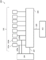
Fig. 1 shows a schematic illustration of a sensor circuit 100 according to an embodiment.
The sensor circuit 100 may comprise a plurality of half-bridge sensor circuits 101. The sensor circuit 100 may further comprise a sensor output value determination circuit 102, the sensor output value determination circuit 102 being configured to determine the sensor output value based on at least one half-bridge sensor signal 103 provided by one of the half-bridge sensor circuits of the plurality of half-bridge sensor circuits 101. The sensor circuit 100 may further include an error determination circuit 104, the error determination circuit 104 configured to generate an error signal 107 based on a first half-bridge sensor signal 105a generated by a first half-bridge sensor circuit 101a of the plurality of half-bridge sensor circuits and a second half-bridge sensor signal 105b generated by a second half-bridge sensor circuit 101b of the plurality of half-bridge sensor circuits.
The sensor circuit 100 may further comprise a control circuit 106, the control circuit 106 being configured to control the selection of one of the first and second half- bridge sensor circuits 101a, 101b based on the error signal 107 for providing one of the first and second half- bridge sensor signals 105a, 105b to the sensor output value determination circuit 102 for determining the sensor output value.
Due to the embodiment of the sensor circuit with a control circuit controlling the selection of one of the first half-bridge sensor circuit and the second half-bridge sensor circuit based on the error signal, the faulty half-bridge sensor circuit may be replaced by, for example, a working half-bridge sensor circuit when an error is detected. This may provide redundancy, which may, for example, improve safety in an automotive installation or vehicle. The complexity of replacing a full-bridge sensor circuit even if only half of the full-bridge sensor circuit fails can also be avoided instead of a half-bridge sensor circuit, for example. This may for example lead to reduced costs.
The sensor circuit 100 may, for example, include a plurality of half-bridge sensor circuits 101 that may be arranged in a plurality of wheatstone bridge formations or arrangements. For example, the plurality of half-bridge sensor circuits 101 may be arranged to form one or more full-bridge sensor circuits each including a pair of half-bridge sensor circuits, for example. The full-bridge sensor circuit may include one half-bridge sensor circuit coupled between a supply voltage terminal and a reference voltage terminal (e.g., a ground terminal) and a complementary half-bridge sensor circuit coupled between the supply voltage terminal and the reference voltage terminal. The complementary half-bridge sensor circuit of the full-bridge sensor circuit may be identical or similar to the half-bridge sensor circuit of the full-bridge sensor circuit, but may be oppositely coupled between the supply voltage terminal and the reference voltage terminal. In other words, the complementary half-bridge sensor circuit of the full-bridge sensor circuit may have a different (e.g., opposite or reversed) polarity with respect to the half-bridge sensor circuit of the full-bridge sensor circuit.
In the arrangement of sensor circuit 100, the half-bridge sensor circuits (e.g., all of the half-bridge sensor circuits) of the plurality of half-bridge sensor circuits 101 may each include a first terminal electrically coupled to the supply voltage terminal and a second terminal electrically coupled to the reference voltage terminal. Each half-bridge sensor circuit 101 may include a pair of resistive elements (e.g., magnetoresistive elements or hall elements) that may be responsive to a stimulus (e.g., an external stimulus). The response of the resistive element to such a stimulus may include, for example, a change in the resistance of the resistive element. Each half-bridge sensor circuit 101 may be configured to generate a half-bridge sensor signal in response to a change in an external environment or stimulus, such as a change in a magnetic field or a change in pressure, for example.
The half-bridge sensor circuit 101 may be configured to generate a half-bridge sensor signal at a half-bridge sensor circuit output terminal (or node). For example, each half-bridge sensor circuit 101 may include a half-bridge sensor circuit output terminal disposed between a first resistive element and a second resistive element of a pair of resistive elements. The half-bridge sensor signal output at the output terminals of the half-bridge sensor circuit may be based on, for example, a voltage or current change due to a change (or imbalance) in the resistive element in response to the excitation. In some examples, the half-bridge sensor signal may be a sinusoidal signal, but is not limited thereto.
The first half-bridge sensor circuit 101a may be part of a first full-bridge sensor circuit. The second half-bridge sensor circuit 101b may be part of a second full-bridge sensor circuit. The second half-bridge sensor circuit 101b may, for example, be identical to the first half-bridge sensor circuit 101a and may be coupled to the supply voltage terminal and the reference voltage terminal with the same polarity as the first half-bridge sensor circuit 101 a. For example, the first half-bridge sensor signal 105a generated by the first half-bridge sensor circuit 101a may be a sinusoidal signal (e.g., a sinusoidal signal) having a first predetermined phase offset. Due to the same polarity and configuration of the first half-bridge sensor circuit 101a, the second half-bridge sensor signal 105b generated by the second half-bridge sensor circuit 101b may also be, for example, a sinusoidal signal (e.g., a sinusoidal signal) with the same first predetermined phase offset. Thus, it is for example possible to replace the first half-bridge sensor circuit 101a with a second half-bridge sensor circuit 101b, if the first half-bridge sensor circuit 101a fails. In other words, the second half-bridge sensor circuit 101b may provide redundancy for the first half-bridge sensor circuit 101 a.
The sensor circuit 100 comprises a sensor output value determination circuit 102, which sensor output value determination circuit 102 may for example be configured to determine a sensor output value based on at least one half-bridge sensor signal 103 provided by a plurality of half-bridge sensor signals. In some examples, the sensor output value determination circuit 102 may be configured to determine the sensor output value based on two or four half-bridge sensor signals, for example. The sensor output value determination circuit 102 may be configured to determine the sensor output value based on one of the first half-bridge sensor signal 105a, the second half-bridge sensor signal 105b, a third half-bridge sensor signal provided by a third half-bridge sensor circuit, and a fourth half-bridge sensor signal provided by a fourth half-bridge sensor circuit. In other words, the sensor output value determination circuit 102 may, for example, be configured to determine the sensor output value based on the first or second half-bridge sensor signal or based on the third or fourth half-bridge sensor signal.
The sensor output value determination circuit 102 may be configured to determine the sensor output value based on the third half-bridge sensor signal and one of the first half-bridge sensor signal 105a and the second half-bridge sensor signal 105 b. The plurality of half-bridge sensor circuits may, for example, include a third half-bridge sensor circuit configured to provide a third half-bridge sensor signal. The sensor output value determination circuit 102 may, for example, be configured to determine the sensor output value further based on a first or second complementary half-bridge sensor signal generated by the first or second complementary half-bridge sensor circuit and based on a third or fourth half-bridge sensor signal generated by the third or fourth complementary half-bridge sensor circuit.
The sensor circuit 100 includes an error determination circuit 104, which may be configured to determine whether a half-bridge sensor circuit is malfunctioning, for example. For example, the error determination circuit 104 may be configured to generate the error signal 107 based on a comparison, addition, and/or subtraction of the first half-bridge sensor signal 105a and the second half-bridge sensor signal 105 b. In an example, the error determination circuit 104 may be configured to compare the first half-bridge sensor signal with the second half-bridge sensor signal 105 b. For example, if the half-bridge sensor signal generated by the half-bridge sensor circuit is a continuous zero signal (e.g., has a zero signal response) rather than a desired sinusoidal signal, the error determination circuit 104 may generate an error signal that indicates a failure of one of the first and second half- bridge sensor signals 105a, 105 b. In another example, the error determination circuit 104 may generate the error signal if the amplitude and/or phase of one of the first and second half-bridge sensor signals deviates from each other by more than a threshold, such as more than 1%, or such as more than 5% or such as more than 10%.
In another example, the error determination circuit 104 may additionally, alternatively, or alternatively be configured to determine a difference between a first half-bridge sensor signal 105a generated by the first half-bridge sensor circuit 101a and a second half-bridge sensor signal 105b generated by the first half-bridge sensor circuit 101 b. Since both the first and second half-bridge sensor circuits are substantially identical, the sensor signals generated by both half-bridge sensor circuits should be similar (e.g., less than 1% amplitude and/or phase deviation of the phase and/or amplitude of one of the signals) if they are functioning properly. The error determination circuit 104 may generate an error signal that may indicate a fault in one of the half-bridge sensor circuits if the difference between the first half-bridge sensor signal 105a and the second half-bridge sensor signal 105b exceeds or falls below a reference threshold (e.g., if the amplitude and/or phase value of the midpoint deviates more than 1% from the phase and/or amplitude value of the midpoint of one of the first half-bridge sensor signal 105a and the second half-bridge sensor signal 105 b). In another example, the error determination circuit 104 may additionally, alternatively, or alternatively be configured to determine a sum of the first and second half- bridge sensor signals 105a, 105 b. The error determination circuit 104 may, for example, generate an error signal that may indicate a fault in at least one of the half-bridge sensor signals if the sum of the first half-bridge sensor signal 105a and the second half-bridge sensor signal 105b exceeds or falls below a reference threshold or deviates from the reference signal.
The error determination circuit 104 may additionally, alternatively or alternatively be configured to generate the error signal 107 based on a comparison, addition and/or subtraction, or determination of a difference, of a further half-bridge sensor signal generated by a further half-bridge sensor circuit of the plurality of half-bridge sensor circuits with the first half-bridge sensor signal 105a or the second half-bridge sensor signal 105 b. The further half-bridge sensor circuit may be, for example, a third or fourth or fifth half-bridge sensor circuit or any one or more half-bridge sensor circuits among the plurality of half-bridge sensor circuits. For example, the error determination circuit 104 may be configured to make the herein described comparisons, additions, and/or subtractions between at least one or both of the first and second half- bridge sensor signals 105a, 105b and further half-bridge sensor signals, which allows a faulty half-bridge sensor circuit to be identified.
The error determination circuit 104 may be configured to communicate an error signal 107 to the control circuit 106 if a fault is detected in at least one of the first and second half- bridge sensor circuits 101a, 101 b. The control circuit 106 may be configured to select or control selection of one of the first and second half- bridge sensor circuits 101a, 101b for providing a half-bridge sensor signal to the sensor output value determination circuit 102. The selection may be based on the error signal 107, for example. If no fault is detected, the error determination circuit 104 may, for example, be configured to transmit an error signal to the control circuit 106 indicating that no fault is detected. In other words, the error signal may indicate the faulty or working bridge to be selected.
The sensor circuit 100 includes a control circuit 106, which control circuit 106 may be configured to control selection of a half-bridge sensor circuit for providing a half-bridge sensor signal used by the sensor output value determination circuit 102 to determine the sensor output value. If the error signal is received by the control circuit 106, the control circuit may be configured to select or control the selection of an operating equivalent half-bridge sensor circuit in place of the failed half-bridge sensor circuit. If no fault is detected, the control circuit 106 may, for example, continue to select or control the selection of the same half-bridge sensor circuit until a fault is finally detected.
The sensor output value determination circuit 102 may be configured to determine a sensor output value based on a half-bridge sensor signal from a selected half-bridge sensor circuit. For example, in a default configuration, the sensor output value determination circuit 102 may be configured to determine the sensor output value based on the first half-bridge sensor signal 105a provided by the first half-bridge sensor circuit 101 a. The error determination circuit 104 may detect a fault in the first half-bridge sensor circuit 101a based on the first half-bridge sensor signal 105a and may transmit an error signal 107 to the control circuit 106. The control circuit 106 may, for example, select or control the selection of the second half-bridge sensor circuit 101b instead of the first half-bridge sensor circuit 101a based on the transmitted error signal 107 for providing the second half-bridge sensor signal 105b for determining a subsequent sensor output value.
The sensor output value determination circuit 102, the error determination circuit 104, the control circuit 106 and/or other optional units may be, for example, separate hardware units or parts of a computer, a digital signal processor or a microcontroller or a computer program or software product for running on a computer, a digital signal processor or a microcontroller. The sensor output value determination circuit 102, the error determination circuit 104, the control circuit 106, and/or other optional components may be implemented independently of one another or may be implemented at least partially together (e.g., on the same die or by the same computer program).
In some examples, the sensor circuit 100 may be implemented as an angle sensor, a magnetic sensor, or a pressure sensor, for example. In an example, the sensor circuit 100 may be a rotation angle sensor. The sensor circuit 100 may be used, for example, to measure the angle of rotation of a rotating portion about a reference axis. Thus, the sensor output value may be, for example, an angle value, a magnetic field value, or a pressure value. In some examples, the sensor circuit 100 may be a rotation angle detection sensor. The sensor circuit 100 may be implemented in an automotive vehicle or device and may be used to measure the angle of rotation of a rotating portion (e.g., a steering wheel) of the automotive vehicle or device that generates a rotating magnetic field axis in a sensitive sensor plane.
In an example, the plurality of half-bridge sensor circuits 101 may include eight half-bridge sensor circuits. For example, the plurality of half-bridge sensor circuits 101 may include four full-bridge sensor circuits. The first full-bridge sensor circuit may be identical to the second full-bridge sensor circuit. The third full-bridge sensor circuit may be different from the first and second full-bridge sensor circuits and may be identical to the fourth full-bridge sensor circuit. The sensor circuit 100 may be configured to determine a sensor output value based on one of the first and second half/bridge sensor circuits and one of the third and fourth half/bridge sensor circuits. The other of the first and second half/bridge sensor circuits and the other of the third and fourth half/bridge sensor circuits may provide redundancy in the event of a failure of the half bridge sensor circuit used to determine the sensor output value. An example is shown in fig. 2.
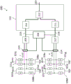
Fig. 2 shows a schematic illustration of a sensor circuit 200 according to an embodiment.
The sensor circuit 200 may be similar to the sensor circuit described with respect to fig. 1. For example, sensor circuit 200 may comprise four full bridge sensor circuits. Each full-bridge sensor circuit may comprise, for example, a half-bridge sensor circuit and a complementary half-bridge sensor circuit.
The sensor circuit 200 may be implemented, for example, as a magnetoresistive (e.g., xMR) angle sensor. For example, each magnetoresistive structure of the half-bridge sensor circuit may be an Anisotropic Magnetoresistive (AMR) structure, a Giant Magnetoresistive (GMR) structure, or a Tunnel Magnetoresistive (TMR) structure. The sensor circuit may be adapted for AMR, GMR or TMR.
Each half-bridge sensor circuit may comprise a pair of magnetoresistive structures as resistive elements. For example, each half-bridge sensor circuit 101 of sensor circuit 200 may include a pair of magnetoresistive structures. Each (or all) of the plurality of half-bridge sensor circuits 101 may each include a first magnetoresistive structure and a second magnetoresistive structure. The first and second magnetoresistive structures may have complementary electrical properties depending on an external magnetic field. The first and second magnetoresistive structures of the same half-bridge sensor circuit may have different predefined reference magnetization directions (indicated by arrows as sensitive magnetization directions). The first and second magnetoresistive structures of the same half-bridge sensor circuit may have opposite predefined reference magnetization directions.
The predefined reference magnetization direction of the magnetoresistive structure may be, but is not limited to, a fixed magnetic orientation of a pinned layer of the magnetoresistive structure. The magnetoresistive structure may include an antiferromagnetic layer. The pinned layer may be held in a fixed magnetic orientation due to exchange biasing effects between the antiferromagnetic layer and the ferromagnetic pinned layer. The sensing layer (or free layer) may be separated from the pinned layer by a nonmagnetic spacer layer. Based on the change in magnetic field caused by the excitation, e.g., due to movement of the magnetic rotating member in proximity to the sensor circuit 200, the magnetoresistive structure of the plurality of half-bridge sensor circuits of the sensor circuit 200 may exhibit a change in resistance. For example, electrons in the free layer of the first magneto-resistive structure may tend to align in a first predefined reference magnetization direction that is identical to the pinned layer of the first magneto-resistive structure. This may cause the first magneto-resistive structure to have a reduced resistance. In addition, electrons in the free layer of the second magneto-resistive structure may tend to align in a direction opposite to the second predefined reference magnetization direction as a pinned layer of the second magneto-resistive structure. This may cause the first magnetoresistive structure to have an increased resistance, but is not limited thereto. The change in resistance and the different responses exhibited by the first and second magnetoresistive structures may cause a change in voltage or current at an output terminal between the first and second magnetoresistive structures of the half-bridge sensor circuit. In other words, a half-bridge sensor signal (e.g., a voltage or current signal) may be generated by a half-bridge sensor circuit that varies (e.g., in a sinusoidal manner) with changes in angular rotation, for example.
Each half-bridge sensor circuit may include a first magnetoresistive structure having a first terminal coupled to a supply voltage terminal and a second terminal electrically coupled in series to a first terminal of a second magnetoresistive structure. The second terminal of the second magnetoresistive structure may be electrically coupled to a reference terminal (e.g., a ground terminal). The oppositely coupled half-bridge sensor circuit may include a first magnetoresistive structure having a first terminal coupled to the reference terminal and a second terminal electrically coupled to the first terminal of the second magnetoresistive structure. The second terminal of the second magnetoresistive structure may be electrically coupled to a supply voltage terminal. Due to the opposite polarity of the complementary half-bridge sensor circuits, a complementary half-bridge sensor circuit in a full-bridge sensor circuit may generate a sinusoidal signal having a 180 ° phase offset with respect to its corresponding other half-bridge sensor circuit in a full-bridge sensor circuit arrangement.
For example, the sensor circuit 200 may include a first full-bridge sensor circuit 108a, the first full-bridge sensor circuit 108a including a first half-bridge sensor circuit 101a and a first complementary half-bridge sensor circuit 108 c. The first half-bridge sensor circuit may comprise a first magneto-resistive structure having a first predefined reference direction (e.g. a 0 ° reference offset) and a second magneto-resistive structure having a second predefined reference direction (e.g. a 180 ° reference offset with respect to the first predefined reference direction). The first half-bridge sensor signal generated by the first half-bridge sensor circuit 101a of the first full-bridge sensor circuit 108a may be, for example, a sinusoidal signal having a first predetermined phase offset (e.g., 0 ° phase offset) with respect to a pure sinusoidal function. The first complementary half-bridge sensor circuit 101c may comprise a first magnetoresistive structure having a same first predefined reference direction (e.g. a 0 ° reference offset) and a second magnetoresistive structure having a second predefined reference direction (e.g. a 180 ° reference offset with respect to the first predefined reference direction). Due to its different (or, e.g., opposite) polarity, the complementary half-bridge sensor signal generated by the first complementary half-bridge sensor circuit 101c of the full-bridge sensor circuit 108a may, for example, be a sinusoidal signal having a second predetermined phase offset (e.g., 180 ° phase offset) with respect to the first predetermined phase offset of the first half-bridge sensor signal. For example, the first half-bridge sensor signal may be a positive sinusoidal signal. Due to its different (or, for example, opposite) polarity, the first complementary half-bridge sensor signal generated by the first complementary half-bridge sensor circuit 101c of the first full-bridge sensor circuit 108a may be a negative sinusoidal signal.
The sensor circuit 200 may further include a second full-bridge sensor circuit 108b, the second full-bridge sensor circuit 108b including a second half-bridge sensor circuit 101b and a second complementary half-bridge sensor circuit 101 d. The second full-bridge sensor circuit may for example be identical to the first full-bridge sensor circuit. Due to the same polarity and configuration as the first half-bridge sensor circuit 101a, the second half-bridge sensor signal generated by the second half-bridge sensor circuit 101b may also be a sinusoidal signal with the same first predetermined phase offset as the first half-bridge sensor signal. The second half-bridge sensor signal may instead be a positive sinusoidal signal. The second complementary half-bridge sensor signal generated by the second complementary half-bridge sensor circuit 101d may have the same second predetermined phase offset as the first complementary half-bridge sensor signal. For example, the second complementary half-bridge sensor signal may be a negative sinusoidal signal.
The sensor circuit 200 may further include a third full-bridge sensor circuit 108c, the third full-bridge sensor circuit 108c including a third half-bridge sensor circuit 101e and a third complementary half-bridge sensor circuit 101 g. The third half-bridge sensor circuit 101c may comprise a first magneto-resistive structure having a third predefined reference direction (e.g. a 90 ° reference offset in a GMR structure) and a second magneto-resistive structure having a fourth predefined reference direction (e.g. a 270 ° reference offset with respect to the first predefined reference direction). The third half-bridge sensor signal generated by the third half-bridge sensor circuit may have a (third) predefined phase offset with respect to at least one of the first half-bridge sensor signal and the second half-bridge sensor signal. For example, the predefined phase offset (for GMR structures) may be a 90 ° phase offset. For example, the third half-bridge sensor signal may be a cosine signal. The third complementary half-bridge sensor circuit 101c may comprise a first magnetoresistive structure having a same third predefined reference direction (e.g. a 90 ° reference offset) and a second magnetoresistive structure having a same fourth predefined reference direction (e.g. a 270 ° reference offset with respect to the first predefined reference direction). Due to its different (or, e.g., opposite) polarity, the third complementary half-bridge sensor signal generated by the third complementary half-bridge sensor circuit 101g of the third full-bridge sensor circuit 108c may be a sinusoidal signal with a (fourth) predetermined phase offset with respect to the first half-bridge sensor signal (e.g., 270 ° phase offset in case of a GMR configuration) and a 180 ° phase offset with respect to the third half-bridge sensor signal. Likewise, the third complementary half-bridge sensor signal may be a negative cosine signal.
The sensor circuit 200 may further include a fourth full-bridge sensor circuit 108d, the fourth full-bridge sensor circuit 108d including a fourth half-bridge sensor circuit 101f and a fourth complementary half-bridge sensor circuit 101 h. The fourth full-bridge sensor circuit may be identical to the third full-bridge sensor circuit without limitation. Due to the equivalent polarity and structure as the third half-bridge sensor circuit 101e, the fourth half-bridge sensor signal generated by the fourth half-bridge sensor circuit 101f may also be, for example, a sinusoidal signal with the same (third) predetermined phase offset as the third half-bridge sensor signal. For example, the fourth half-bridge sensor signal may be a positive cosine signal. The fourth complementary half-bridge sensor signal generated by the fourth complementary half-bridge sensor circuit 101h may have the same (fourth) predetermined phase offset as the third complementary half-bridge sensor signal. The fourth complementary half-bridge sensor signal 101h may be a negative cosine signal without limitation.
In a default selection, the first full-bridge circuit 108a and the third full-bridge circuit 108c may be selected by the control circuit 106 for determining the sensor output value based on the half-bridge sensor signals provided by the first full-bridge circuit and the third full-bridge circuit. The control circuit 106 may be configured to control or may include at least one multiplexer circuit (e.g., multiplexer circuit 214) configured to select at least one further half-bridge sensor circuit of the plurality of half-bridge sensor circuits and at least one of the first half-bridge sensor circuit and the second half-bridge sensor circuit for providing a half-bridge sensor signal for generating the sensor output value. For example, the first half-bridge sensor signal, the first complementary half-bridge sensor signal, the third half-bridge sensor signal, and the third complementary half-bridge sensor signal may be used by the sensor output value determination circuit 102 to determine the sensor output value. In an example, each of these signals may be communicated to the sensor output value determination circuit 102. For example, the sensor output value determination circuit 102 may be configured to determine the sensor output value based on the first half-bridge sensor signal V1+ (e.g., + sin θ signal) and the third half-bridge sensor signal V3+ (e.g., + cos θ signal). Further, the sensor output value determination circuit 102 may be configured to determine the sensor output value based on the first complementary half-bridge sensor signal V1- (e.g., -sin θ signal) and the third complementary half-bridge sensor signal V3- (e.g., -cos θ signal). In another example, a signal based on the sum of the selected half-bridge sensor signals may be communicated to the sensor output value determination circuit 102. For example, signals V3 and V1 may be transmitted to the sensor output value determination circuit 102, where V3 = V3+ -V3- (cosine signal) and V1 = V1+ -V1- (sine signal). In some examples, the sinusoidal signal may be transmitted to the sensor output value determination circuit 102, for example, via the first transmission path 215. The cosine signal may be transmitted to the sensor output value determination circuit 102 via the second transmission path 216, for example.
The sensor circuit 200 may further comprise at least one analog-to-digital converter (ADC) circuit 209, the analog-to-digital converter circuit 209 being configured to generate a digital sensor signal based on an analog half-bridge sensor signal provided by the half-bridge sensor circuit selected by the control circuit. The ADC circuit may be configured to generate a digital sensor signal based on an analog half-bridge sensor signal provided by the half-bridge sensor circuit selected by the at least one multiplexer circuit. The ADC circuit may be electrically coupled between a plurality of half-bridge sensor circuits and the sensor output value determination circuit 102, for example. The sensor circuit 200 may comprise a first ADC circuit 209 coupled to the first and second full-bridge sensor circuits and the sensor output value determination circuit 102. For example, the first ADC circuit 209 may be further electrically coupled to the control circuit 106 and the sensor output value determination circuit 102. The first ADC circuit 209 may, for example, be configured to generate a first digital sensor signal based on a sinusoidal signal, for example, based on at least one of a first half-bridge sensor signal (V1 +) and a first complementary half-bridge sensor signal (V1-). For example, the first ADC circuit may be configured to generate a digital sensor signal based on an addition or subtraction of the first half-bridge sensor signal (V1 +) and the first complementary half-bridge sensor signal (V1-). The first digital sensor signal may be transmitted to the sensor output value determination circuit 102 via a first transmission path 215. Similarly, the sensor circuit 200 may include a second ADC circuit 217 electrically coupled to the third and fourth full-bridge sensor circuits and the sensor output value determination circuit 102. For example, the second ADC circuit 217 may be further electrically coupled to the control circuit 106 and the sensor output value determination circuit 102. The second ADC circuit 217 may be configured to generate a second digital sensor signal based on a cosine signal, for example, at least one of a third half-bridge sensor signal (V3 +) and a third complementary half-bridge sensor signal (V3-). The second digital sensor signal may be transmitted to the sensor output value determination circuit 102 via a second transmission path 216. The second digital sensor signal may for example also be used for determination of the sensor output value.
The sensor output value determination circuit 102 may be configured to perform digital signal processing of the received digital sensor signal, for example. The sensor output value determination circuit 102 may be a digital signal processor. For example, the sensor circuit may further include an amplitude offset correction circuit 209 configured to correct an amplitude offset of the digital sensor signal. The amplitude offset correction circuit 211 may be used to correct for offset (e.g., offset caused by temperature drift or temperature drift). For example, the sensor output value may be determined based on the corrected digital sensor signal. In an example, the amplitude offset correction circuit 211 may be part of the sensor output value determination circuit 102. The sensor output value determination circuit 102 may include an angle calculation circuit 212 configured to determine or calculate a sensor output value, which may be an angle value.
In an example of a default operating mode, the first half-bridge sensor circuit and the first complementary half-bridge sensor circuit of the first full-bridge sensor circuit and the third half-bridge sensor circuit and the third complementary half-bridge sensor circuit of the third full-bridge sensor circuit may be selected by the control circuit 106 for each providing a half-bridge sensor signal for determining the sensor output value. Accordingly, the sensor output value determination circuit 102 may be configured to determine the sensor output value based on the first half-bridge sensor signal V1+ (e.g., + sin θ signal) and the third half-bridge sensor signal V3+ (e.g., + cos θ signal). The sensor output value may be based on or equal to θ, which may be calculated based on the first half-bridge sensor signal and the third half-bridge sensor signal. For example, θ may be a value based on or equal to the angle of rotation, for example. θ may be based, for example, on the first half-bridge sensor signal and the third half-bridge sensor signal by arctangent (e.g., arc tan or t)an -1) Calculated to obtain. To provide angular measurement accuracy within 360 °, the sensor output value determination circuit 102 may, for example, be configured to determine the sensor output value additionally based on the first complementary half-bridge sensor signal V1- (e.g., -sin θ signal) and the third complementary half-bridge sensor signal V3- (e.g., -cos θ signal). The sensor output value may be determined based on the corrected digital half-bridge signals (e.g., the digitally corrected first and third half-bridge sensor signals, and the digitally corrected first and third complementary half-bridge sensor signals).
The sensor output value determination circuit 102 may be configured to determine the sensor output value based on an equationtan -1V1/V3 to determine a sensor output value, e.g., θ.
The sensor circuit 200 may, for example, further comprise an output interface circuit 212 configured to transmit the sensor output value to a receiver. The error determination circuit 104 may be configured to perform a comparison, addition, and/or subtraction of the half-bridge sensor signals of the plurality of half-bridge sensor circuits during the transfer of the sensor output values by the output interface circuit 212.
To determine a faulty or working half-bridge sensor circuit, the error determination circuit 104 may contain a test circuit configured to provide test instructions to the at least one multiplexer circuit 214 for controlling selection of the half-bridge sensor (test) signals. For example, multiplexer circuit 214 may be configured to select at least one reference terminal (e.g., a ground reference terminal) and at least one first half bridge sensor signal. The first half-bridge sensor selected by the multiplexer circuit 214 may be converted to a digital first half-bridge sensor signal, for example, by an ADC, and communicated to the error determination circuit 104 and stored. Subsequently, the multiplexer circuit 214 may be configured to select the at least one reference terminal (e.g., a ground reference terminal) and the at least one second half-bridge sensor signal. The second half-bridge sensor selected by the multiplexer circuit 214 may be converted to a digital second half-bridge sensor signal, for example, by an ADC, and communicated to the error determination circuit 104 and stored. The error determination circuit 104 may be configured to perform the comparison, addition, and/or subtraction based on the first and second digital half-bridge sensor signals.
In an example, based on the test instructions, the at least one multiplexer circuit 214 may be configured to select the first half-bridge sensor signal and the second half-bridge sensor signal together. The first half-bridge sensor signal may be ADC-converted to a digital first half-bridge sensor signal by a first ADC circuit, while the second half-bridge sensor signal may be ADC-converted to a digital second half-bridge sensor signal by a second ADC circuit before being passed to the error determination circuit 104.
In an example, based on the test instructions, the multiplexer circuit 214 or the further multiplexer circuit may be configured to select at least one further half-bridge sensor circuit of the plurality of half-bridge sensor circuits and at least one of the first half-bridge sensor circuit 101a and the second half-bridge sensor circuit 101b for providing a half-bridge sensor signal for generating the error signal.
The detection of a faulty half-bridge sensor circuit by the error determination circuit 104 may be based on a comparison, addition or subtraction of the (digital) first half-bridge sensor signal 101a with the (digital) second half-bridge sensor signal 101b and a further comparison, addition or subtraction of at least one further (digital) half-bridge sensor signal with the (digital) first half-bridge sensor signal 101a and the (digital) second half-bridge sensor signal 101 b.
The at least one multiplexer circuit 214 may be electrically coupled to the control circuit 106 or may be part of the control circuit 106, for example. Based on the comparison (or addition or otherwise) of the half-bridge sensor signals, if any of the half-bridge sensor circuits fails, the error determination circuit 104 may be configured to generate an error signal, and the control circuit 106 may be configured to select a properly functioning half-bridge sensor circuit, for example, in place of the failed half-bridge sensor circuit. The error determination circuit 104 (e.g., test circuit) may be configured to generate an error signal during transmission of the sensor output value through the output interface circuit 213. For example, the test circuitry may provide test instructions during the transmission of the output parameters and/or directly after the determination of the sensor output values and before the determination of successive sensor output values. In this manner, the dead time may be used to perform a testing procedure to increase the reliability and/or usability of the sensor circuit 200.
Alternatively, the test circuit may repeatedly carry out the test after transmitting a predefined number of values of the output parameter (e.g. after each, every second value, every third value, every tenth value, or another integer number). Repeating the test n times per transmitted output parameter may be sufficient to significantly improve the reliability and/or usability of the sensor circuit. Alternatively or additionally, the test circuit may repeatedly perform the test at equal time intervals. For example, the test circuit may perform the test at repeated time intervals. The repeating time interval may comprise a length between 1ms and 50ms (or between 2ms and 20ms, or between 5ms and 10ms, such as 1ms, 5ms, 10ms, or 20 ms).
The control circuit 106 (e.g., including the multiplexer 214) may be configured to select or control selection of the second half-bridge sensor circuit 101b to replace the first half-bridge sensor circuit 101 based on the error signal (e.g., if the first half-bridge sensor circuit is determined to be faulty). The half-bridge sensor signal from the (newly selected) second half-bridge sensor circuit 101b may then be used to determine a subsequent sensor output value in a subsequent measurement. If no fault is detected in the error determination circuit 104, the control circuit 106 may, for example, continue to select or control the selection of the first half-bridge sensor circuit 101a for providing the half-bridge sensor signal to the sensor output value determination circuit 102. In other words, the control circuit 106 may for example be configured to select or control the selection of one of the first and second half- bridge sensor circuits 101a, 101b during the transfer of the sensor output value through the output interface circuit.
Replacing a faulty half-bridge sensor circuit with an equivalent (redundant) half-bridge sensor circuit can avoid the complexity of replacing a full-bridge sensor circuit even if only half of the full-bridge sensor circuit fails. This may for example lead to reduced costs.
For angle sensors, a safety objective may be to guarantee a dedicated angle accuracy within a predefined time (e.g. a 5 ° deviation of the true angle value may have to be detected within 5 ms). The challenge to be overcome may be how to guarantee the validity of the sensed value without the second independent sensing element. The xMR angle sensor may have two different wheatstone sensor bridges, each generating a sinusoidal signal, e.g. one sine component and one cosine component. This dual signal generation is well suited for safety critical applications because of the use of two different signal paths. It will be noted that the use of two signal paths yields only a single signal angle value. Once this single angle signal is generated, the redundancy (provided by the two individual signal paths) is lost. For safety critical applications, it may be of interest to provide the availability of programmable units (such as angle sensors) or even to enhance the availability. When using the methods described above, redundancy is lost while benefiting from the increased reliability of the angle sensor or system. The system is still operational and therefore usable even if one of the half-bridges fails or is identified as unreliable.
It may seem contradictory that one of the key elements of functional safety is to indicate an error immediately and to provide information that the dedicated sensor value is no longer valid. However, in such a case, a warning may be provided or the transmission of sensor information as in indicating the measurement angle may be stopped. The error correction unit may be responsible for reacting to meet safety requirements to cause redundancy in availability. High ASIL levels and high availability may be achieved, for example, by combining sensors and doubling signal paths. High availability may increase ASIL levels. In case one (first) path shows an error, the second path may be used for functional and security purposes, for example. In other words, if the first path shows an error, an alert may be issued and/or the signal received from the first path may be ignored or overwritten. It may be of interest to implement a plurality of sensor elements based on xMR technology as a non-limiting example.
Two (full) bridges may be used for the angle sensor to allow extraction of sine and cosine signals. To some extent, the information provided may be redundant (sine and cosine), but it may for example be used only for security or usability purposes due to the correlation between the two (e.g. between sine and cosine signals).
Further details and aspects are mentioned in connection with the above or below described embodiments (e.g. half bridge sensor circuit, full bridge sensor circuit, sensor output value determining circuit, magneto resistive structure, error determining circuit, control circuit and sensor output value determining circuit). The embodiment shown in fig. 2 may include one or more optional additional features corresponding to one or more aspects mentioned in relation to the proposed concept or one or more embodiments described above (e.g., fig. 1) or below (e.g., fig. 3-7).
Fig. 3 shows a schematic illustration of a sensor circuit according to an embodiment. The sensor circuit 300 may be similar to the sensor circuits described in fig. 1 and/or 2.
The sensor circuit 300 may be implemented in at least one semiconductor substrate, for example. The semiconductor substrate may be, for example, a semiconductor die or may comprise part of a semiconductor wafer. The semiconductor substrate may be, for example, a silicon-based semiconductor substrate, or a silicon carbide-based semiconductor substrate, or a gallium arsenide-based semiconductor substrate, or a gallium nitride-based semiconductor substrate.
In the sensor circuit 300, each default full-bridge sensor circuit (e.g., 108 a) may be formed proximate to an identical redundant full-bridge sensor circuit (e.g., 108 b). The (redundant) full-bridge sensor circuit (e.g., 108 b) may, for example, have a magnetoresistive structure equivalent to the default full-bridge sensor circuit (e.g., 108 a), and may also be coupled between a supply voltage (e.g., VDD) and a reference voltage (e.g., ground GND) with a polarity equivalent to the default full-bridge sensor circuit.
In addition, each default half-bridge sensor circuit may be formed adjacent to an equivalent redundant half-bridge sensor circuit. For example, a first (default) half-bridge sensor circuit 101a may be formed adjacent to a second (redundant) half-bridge sensor circuit 101b, for example. Similarly, a first (default) complementary half-bridge sensor circuit 101c may be formed adjacent to a second complementary (redundant) half-bridge sensor circuit 101d, for example. Similarly, a third (default) half-bridge sensor circuit 101e may be formed adjacent to a fourth complementary (redundant) half-bridge sensor circuit 101f, for example. Similarly, a third (default) complementary half-bridge sensor circuit 101g may be formed adjacent to the fourth complementary (redundant) half-bridge sensor circuit 101h, for example.
Due to the arrangement of the default half-bridge sensor circuit adjacent to the equivalent (redundant) half-bridge sensor circuit, redundancy may for example be obtained and the redundant half-bridge sensor circuit may be exposed to the same magnetic field conditions as the default half-bridge sensor circuit. Thus, errors due to different field conditions experienced between the original half-bridge sensor circuit and the corresponding redundant half-bridge sensor circuit, for example, may be reduced or eliminated if the original half-bridge sensor circuit is replaced by the corresponding redundant half-bridge sensor circuit.
For example, the plurality of half-bridge sensor circuits may be arranged such that a (e.g. default) magnetoresistive structure having a predefined reference magnetization direction may be formed adjacent to an equivalent (e.g. redundant) magnetoresistive structure having the same predefined reference magnetization direction. For example, the first (default) magnetoresistive structure 318 of the first half-bridge sensor circuit 101a having a first predefined reference magnetization direction1For example, a first (redundant) magnetoresistive structure 318, which may be adjacent to a second half-bridge sensor circuit 101b having the same first predefined reference magnetization direction3Is formed. Similarly, the second magnetoresistive structure 318 of the first half-bridge sensor circuit 101a having a second predefined reference magnetization direction2For example, a second magnetoresistive structure 318 which may be adjacent to a second half-bridge sensor circuit 101b having a same second predefined reference magnetization direction4Is formed.
In the examples described herein (above or below), the terms "adjacent" or "adjacently" are used herein to mean that adjacent elements are placed alongside or next to each other. For example, the magnetoresistive structure may have at least one lateral edge or plane facing an adjacent magnetoresistive structure. For example, between about 50% and about 100% of a lateral edge or surface of a magnetoresistive structure may directly face a lateral edge of an adjacent magnetoresistive structure. The terms "adjacent" or "adjacently," for example, are also used herein to emphasize the proximity of adjacent elements as compared to other elements. In particular, the region between the adjacent default half-bridge sensor circuit and its redundant equivalent half-bridge sensor circuit may be free of other half-bridge sensor circuits, for example. In other words, no other half-bridge sensor circuit may be formed in the region between the default half-bridge sensor circuit and the redundant half-bridge sensor circuit. For example, the region between the first (default) half-bridge sensor circuit 101a and the second (redundant) half-bridge sensor circuit 101b may be free of other half-bridge sensor circuits (particularly half-bridge sensor circuits having unequal magnetoresistive structures as the first and second half-bridge sensor circuits 101 b).
In an example, the first full-bridge sensor circuit and the second full-bridge sensor circuit may also be formed adjacently on a common semiconductor substrate. For example, the first and second half- bridge sensor circuits 101a, 101b may be adjacently formed on a common semiconductor substrate. For example, a (first) magnetoresistive structure (e.g. 318) with a first predefined reference magnetization direction1And 3183) May be formed in a first common region of a common semiconductor substrate. Magnetoresistive structures having the same (e.g., first) predefined reference magnetization direction may be formed in the first common region. For example, the (first) magnetoresistive structures of the first half-bridge sensor circuit 101a and the second half-bridge sensor circuit 101b having the same first predefined reference magnetization direction may be formed in a first common region. For example, no magnetoresistive structure having a predefined reference magnetization direction different from the first predefined reference magnetization direction is formed in the first common region. The default magnetoresistive structure (e.g., of the first half-bridge sensor circuit) may be spatially separated from the redundant equivalent magnetoresistive structure (e.g., of the second half-bridge sensor circuit) by a distance in a lateral or horizontal direction substantially parallel to the major surface of the semiconductor substrate.
(second) magnetoresistive structure (e.g. 318) with second predefined reference magnetization direction2And 3184) May be formed in a second common region of the common semiconductor substrate. Similarly, the (second) magnetoresistive structures of the first and second half- bridge sensor circuits 101a, 101b having the same second predefined reference magnetization direction may be formed in a second common region. For example, no magnetoresistive structure having a predefined reference magnetization direction different from the second predefined reference magnetization direction is formed in the second common region.
The second common area may be different from the first common area. For example, the first common area and the second common area may be adjacent (or, for example, directly adjacent common areas). In some examples, the first common area and the second common area may have a horizontal separation. For example, the first common region and the second common region may be formed, for example, on the same level on the semiconductor substrate. The second common region and the first common region may have a lateral spatial separation within the same level of the semiconductor substrate. A level may refer to a (substantially horizontal) level substantially parallel to a plane of a main surface of a semiconductor substrate, wherein the diameter of the main surface may be more than at least 10 to 100 times the thickness of the semiconductor substrate, for example.
In other examples, the first common area and the second common area may have a vertical separation. The first magnetoresistive structure of the first and second half- bridge sensor circuits 101a, 101b having the same first predefined reference magnetization direction may be formed in a first level. Furthermore, the second magnetoresistive structure of the first and second half- bridge sensor circuits 101a, 101b with a second predefined reference magnetization direction may be formed at a second level of the common semiconductor substrate. For example, the first and second half- bridge sensor circuits 101a, 101b may each comprise, for example, vertically stacked magnetoresistive structures. For example, the second level may have a vertical spatial offset from the first level orthogonal to the main surface of the common semiconductor substrate.
The half-bridge sensor circuits of the third and fourth full-bridge sensor circuits may also be arranged, for example, according to similar principles as the first and second full-bridge sensor circuits. For example, magnetoresistive structures having the same third predefined reference magnetization direction may be formed in a third common region of the semiconductor substrate, and magnetoresistive structures having the same fourth predefined reference magnetization direction may be formed in a fourth common region of the semiconductor substrate. The third and fourth full-bridge sensor circuits may be formed, for example, on the same or different semiconductor substrate as the first and second full-bridge sensor circuits.
The first magnetoresistive structure (of each half-bridge sensor circuit) may be electrically coupled to the second magnetoresistive structure (of the same half-bridge sensor circuit) via, for example, one or more electrically conductive structures (e.g., electrical interconnects). The electrical interconnect may comprise copper or aluminum or any electrically conductive material, for example.
Fig. 3 further shows a schematic arrangement of half-bridges for two angle sensors; the arrows indicate, for example, the reference magnetization direction in the case of resistors based on GMR or TMR structures. The schematic arrangement shows 8 half-bridges (e.g. two full-bridge sensors). For magnetoresistive resistors based on AMR technology, for example, different reference magnetization directions can be represented by different current directions.
Two spatially separated sensors with two sine and cosine bridges can be used to achieve the redundancy effect. In the event of a failure of one sensor or half bridge of one full bridge, this full bridge may no longer be considered for data acquisition, but instead a second full bridge may be selected. However, depending on the magnetic circuit, two spatially separated sensors may be exposed to different field conditions. As a result, the redundant sensor bridge may not completely replace the damaged one. To achieve comparable performance of the two sensors, the two sensors cannot be placed at their optimal positions with respect to the external magnetic field. Thus, sensor accuracy may be reduced.
The sensor circuit described herein may contain at least two magnetic sensors with coiled/interleaved half-bridges. Equivalent resistors and half-bridges, respectively, may be placed next to each other and may thus be exposed to almost equivalent field conditions. In summary, 8 half-bridges are connected in parallel, for example, to generate 8 half-bridge sensor signals.
The functionality of each half-bridge can be checked by measuring the differential output signals of two adjacent identical half-bridges; due to almost identical field conditions, both half-bridges should exhibit substantially the same signal. In case one of the half bridges of the same kind is broken, a different signal is measured and a further check may be initiated to identify the broken half bridge. It may be of interest to use a third half-bridge and to consult the corresponding third half-bridge signal in order to decide which of the two half-bridges showing different signals appears to be damaged. As a further step, half-bridges identified as damaged may be excluded from future evaluations. If one half bridge is identified as damaged, other adjacent half bridges may be selected for angle calculation because the second half bridge is exposed to substantially the same field conditions; for example, the half-bridge arrangement according to the invention provides practical redundancy.
In the case of GMR or TMR sensor structures, locally different reference magnetizations can be provided. One possible technique is a laser magnetization process, in which a resistor is locally heated and cooled above a critical temperature (blocking temperature) within a magnetic field. The examples described herein may allow for local heating of all 4 resistors with identical reference magnetization directions, thereby saving processing time and active area size.
Further details and aspects are mentioned in connection with the above or below described embodiments (e.g. half bridge sensor circuit, full bridge sensor circuit, sensor output value determining circuit, magneto resistive structure, error determining circuit, control circuit, sensor output value determining circuit, arrangement of magneto resistive structures, common area of semiconductor substrate and level of semiconductor substrate). The embodiment shown in fig. 3 may include one or more optional additional features corresponding to one or more aspects mentioned in relation to the proposed concept or one or more embodiments described above (e.g., fig. 1 and 2) or below (e.g., fig. 4-7).
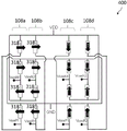
Fig. 4 shows a schematic illustration of a sensor circuit 400 according to an embodiment. The sensor circuit 400 may be similar to the sensor circuits described in fig. 1-3.
In the sensor circuit 400, a first (default) full-bridge sensor circuit 108a, for example, may be formed adjacent to a second (redundant) full-bridge sensor circuit 108 b. Similarly, a third (default) full-bridge sensor circuit 108c may be formed adjacent to the fourth (redundant) full-bridge sensor circuit 108d, for example.
Furthermore, for example, the plurality of half-bridge sensor circuits may be arranged such that all magnetoresistive structures having the same first predefined reference magnetization direction are formed in a first common region (or first level) and all magnetoresistive structures having the same predefined second reference magnetization direction are formed in a second common region (at the same first or second level).
First magnetoresistive structure 318 of first half-bridge sensor circuit 101a and second half-bridge sensor circuit 101b1、3183And a magnetoresistive structure 318 of a first and a second complementary half-bridge sensor circuit having the same first predefined reference magnetization direction10、31812May be formed in the first common region (or first level). Furthermore, the magnetoresistive structures of the first and second half- bridge sensor circuits 101a, 101b having the same first predefined reference magnetization direction may be formed adjacent to each other, and the magnetoresistive structures of the first and second complementary half- bridge sensor circuits 101a, 101b having the same first predefined reference magnetization direction may be formed in a first common region adjacent to each other. Second magnetoresistive structure 318 of first half-bridge sensor circuit 101a and second half-bridge sensor circuit 101b2、3184And a second magnetoresistive structure 318 of the first and second complementary half-bridge sensor circuits having a same second predefined reference magnetization direction9、31811For example, may be formed in the second common region (in the same level as the first common region, or in a second level).
Furthermore, the magnetoresistive structures of the first and second complementary half- bridge sensor circuits 101a, 101b having the same second predefined reference magnetization direction may be formed adjacent to each other, and the magnetoresistive structures of the first and second complementary half- bridge sensor circuits 101a, 101b having the same second predefined reference magnetization direction may be formed in a second common region adjacent to each other.
The half-bridge sensor circuits of the third and fourth full-bridge sensor circuits may also be arranged, for example, according to similar principles as the first and second full-bridge sensor circuits.
Fig. 4 further shows a schematic arrangement and circuitry of a single resistor (or magneto-resistive structure) for optimal positioning for efficient laser magnetization process. The (or all) resistors (or magneto-resistive structures) with identical reference magnetization directions are close together or next to each other, thereby enabling simultaneous magnetization (e.g. using a fast laser magnetization process). The vertical stack may, for example, remove unwanted effects from different field conditions for at least two sensor bridges, but the laser magnetization process may take twice as long.
In other examples, the redundant half-bridge circuit may have a reference direction offset with respect to a default half-bridge circuit that the redundant half-bridge circuit may replace in the event of a fault. For example, an angle sensor with two full bridges may be provided. Each full bridge may be combined with half bridges of the VsinP and VsinN (sin bridge) and VcosP and VcosN (cos bridge) type, respectively. Furthermore, for example, full-bridge signals with VsinP and VcosP (sin 45 ° bridge) and VsinP and VcosN (cos 45 ° bridge) can be generated (for example by redundant half-bridge circuits). The sin 45 ° signal may be a signal phase-shifted by 45 ° with respect to the sine bridge, and the cos 45 ° signal may be a signal phase-shifted by 45 ° with respect to the cosine signal, respectively. The bridge output signals being sin and cos bridge signals
. The angle error remains the same with respect to phase and height.
In other examples, further checks may be applied. For example, signals of the Vsinp/VcosP bridge and the Vsinn/VcosN bridge may be used to verify the functionality of the corresponding half-bridge. Generally speaking, the functionality of the main (or default) half-bridge can be evaluated by different half-bridge combinations.
The sensor circuit described herein may enhance the usability of xMR (AMR, GMR and TMR) sensors by adding at least one further sensor structure (e.g. four different half-bridge types). Equivalent half-bridges may be placed next to each other. Thereby, a substantial redundancy is provided and the processing time for the magnetization process and the active area size can be reduced. Furthermore, resistors with identical reference magnetizations can also be placed next to each other. Furthermore, a check/verification of all half-bridges by connection of an orthogonal half-bridge type to a full-bridge may be performed. The sensor signals from the quadrature half-bridge type may be adapted to provide sufficient information for reliable angle calculation even if both structures of one half-bridge type within two full-bridge arrangements fail.
Further details and aspects are mentioned in connection with the above or below described embodiments (e.g. half bridge sensor circuit, full bridge sensor circuit, sensor output value determining circuit, magneto resistive structure, error determining circuit, control circuit, sensor output value determining circuit, arrangement of magneto resistive structures, common area of semiconductor substrate and level of semiconductor substrate). The embodiment shown in fig. 4 may include one or more optional additional features corresponding to one or more aspects mentioned in relation to the proposed concept or one or more embodiments described above (e.g., fig. 1 to 3) or below (e.g., fig. 5 to 7).
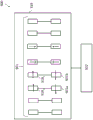
Fig. 5 shows a schematic illustration of a semiconductor device 500 according to an embodiment.
The semiconductor arrangement 500 comprises a plurality of half-bridge sensor circuits 501 each comprising a pair of magnetoresistive structures. The semiconductor device includes a sensor output value determination circuit 502, the sensor output value determination circuit 502 being configured to determine a sensor output value based on at least four half-bridge sensor signals provided by four of the half-bridge sensor circuits of the plurality of half-bridge sensor circuits. A first half-bridge sensor circuit 501a and a second half-bridge sensor circuit 501b of the plurality of half-bridge sensor circuits are formed on a common semiconductor substrate 519. Magnetoresistive structure 518 with a second half-bridge sensor circuit3Magnetoresistive structure 518 of a first half-bridge sensor circuit having the same predefined reference magnetization direction1Are formed adjacent on a common semiconductor substrate 519.
Redundancy may be obtained in that the magnetoresistive structures of the first half-bridge sensor circuit having the same predefined reference magnetization direction as the magnetoresistive structures of the second half-bridge sensor circuit are formed adjacent on a common semiconductor substrate. Redundancy may be obtained because the redundant half-bridge sensor circuit may be exposed to a substantially similar magnetic field as the default half-bridge sensor circuit, for example. Thus, errors or differences caused by different field conditions between the original (e.g., default) half-bridge sensor circuit and its replacement (redundant) half-bridge sensor circuit may be reduced or eliminated, for example. Furthermore, the active area size of the half-bridge sensor circuit and the processing time for the magnetization process can be reduced.
The sensor circuit 500 may further include an error determination circuit 104 and a control circuit 106. In some examples, the error determination circuit 104, the control circuit 106, and the sensor output value determination circuit 502 may be formed on different semiconductor substrates. In some examples, the error determination circuit 104, the control circuit 106, and the sensor output value determination circuit 102 may be formed on the same semiconductor substrate. For example, they may be formed on the same common semiconductor substrate as the one or more half-bridge sensor circuits.
Further details and aspects are mentioned in connection with the above or below described embodiments (e.g. half bridge sensor circuit, full bridge sensor circuit, sensor output value determining circuit, error determining circuit, control circuit, sensor output value determining circuit, arrangement of magnetoresistive structures, common area of semiconductor substrate and level of semiconductor substrate). The embodiment shown in fig. 5 may include one or more optional additional features corresponding to one or more aspects mentioned in relation to the proposed concept or one or more embodiments described above (e.g., fig. 1 to 4) or below (e.g., fig. 6 to 7).
Fig. 6 shows a flow diagram of a method 600 for providing a sensor output value according to an embodiment.
The method 600 may include determining 610 a sensor output value based on at least one half-bridge sensor signal provided by a half-bridge sensor circuit of a plurality of half-bridge sensor circuits.
The method 600 may further include determining 620 an error signal based on a first half-bridge sensor signal generated by a first half-bridge sensor circuit of the plurality of half-bridge sensor circuits and a second half-bridge sensor signal generated by a second half-bridge sensor circuit of the plurality of half-bridge sensor circuits.
The method 600 may further include selecting 630 one of the first half-bridge sensor circuit and the second half-bridge sensor circuit based on the error signal. It may be of interest to use a selected half-bridge circuit to provide one of the first half-bridge sensor signal and the second half-bridge sensor signal to the sensor output value determining circuit. The provided half-bridge sensor signal may further be used for determining the sensor output value.
The method allows identification of a faulty half-bridge sensor circuit. Once a faulty half-bridge sensor circuit is identified, it can be replaced by a working half-bridge sensor circuit. Replacing a half-bridge sensor circuit may be beneficial over replacing a full-bridge sensor circuit. This is of particular interest if only one of the full bridge sensor circuits is faulty. This may for example lead to reduced costs.
Method 600 may further include determining an error signal based on a comparison, addition, and/or subtraction of the first half-bridge sensor signal and the second half-bridge sensor signal, but is not limited thereto.
The method 600 may further include determining an error signal based on a comparison, addition, or subtraction of at least one half-bridge sensor signal generated by the plurality of half-bridge sensor circuits to at least one of the first half-bridge sensor signal and the second half-bridge sensor signal. In a non-limiting example, the method may include determining the error signal based on a sampling of a signal value of the at least one half-bridge sensor signal and a sampling of a signal value of at least one of the first half-bridge sensor signal and the second half-bridge sensor signal. In a non-limiting example, the sampled values of the at least one half-bridge sensor signal may be compared to the sampled values of the first half-bridge sensor signal and/or the second half-bridge sensor signal. In a further non-limiting example, the deviation may be determined based on a subtraction or addition of the at least one half-bridge sensor signal and a sampled signal value of the first half-bridge sensor signal and/or the second half-bridge sensor signal. As described with respect to the previous figures, the method may comprise: the error signal is determined if the amplitude and/or phase of one of the first half-bridge sensor signal and the second half-bridge sensor signal deviates from each other by more than a threshold value, for example by more than 1%, or for example by more than 5% or for example by more than 10%. In further non-limiting examples, the deviation may be compared to one or more thresholds, and an error signal may be determined or generated based on the comparison.
Further details and aspects are mentioned in connection with the above or below described embodiments (e.g. half bridge sensor circuit, sensor output value determining circuit, error determining circuit, control circuit and sensor output value determining circuit, determining sensor output value, providing half bridge sensor signal by half bridge sensor circuit, determining error signal, selecting half bridge sensor circuit and providing half bridge sensor signal to sensor output value determining circuit). The embodiment shown in fig. 6 may include one or more optional additional features corresponding to one or more aspects mentioned in relation to the proposed concept or one or more embodiments described above (e.g., fig. 1 to 5) or below (e.g., fig. 7).
Fig. 7 shows a flow diagram of a method 700 for forming a sensor circuit according to an embodiment.
The method 700 includes forming 710 a plurality of magnetoresistive structures having a first predefined reference magnetization direction in a first common region of a common semiconductor substrate.
The method 700 may further include forming 720 a plurality of magnetoresistive structures having a second predefined reference magnetization direction in a second common region of the common semiconductor substrate.
The method 700 may further include forming 730 an electrically conductive structure electrically coupling a magnetoresistive structure having a first predefined reference magnetization direction to a magnetoresistive structure having a second predefined reference magnetization direction to form a plurality of half-bridge sensor circuits. Each half-bridge sensor circuit includes a magnetoresistive structure having a first predefined reference magnetization direction electrically coupled to a second magnetoresistive structure having a second predefined reference magnetization direction.
Since the magnetoresistive structures with the same predefined reference magnetization direction are formed in the same common region, the active area size of the half-bridge sensor circuit and the processing time for the magnetization process can be reduced. Furthermore, this may result in reduced costs.
The method 700 may further include forming an electrically conductive structure. The electrically conductive structure may electrically couple a first magneto-resistive structure having a first predefined reference magnetization direction to a second magneto-resistive structure having a second predefined reference magnetization direction, thus forming a first half-bridge sensor circuit.
Furthermore, the formation of the second half-bridge sensor circuit may be performed. The second half-bridge sensor circuit may be formed by providing an electrically conductive structure electrically coupling a further first magneto-resistive structure having a first predefined reference magnetization direction to a further second magneto-resistive structure having a second predefined reference magnetization direction. The second half-bridge sensor circuit may be formed adjacent to the first half-bridge sensor circuit. A further first magnetoresistive structure may be formed adjacent to the first magnetoresistive structure, and a further second magnetoresistive structure may be formed adjacent to the second magnetoresistive structure, but is not limited thereto.
At least part of the process for forming the plurality of magnetoresistive structures having the first predefined reference magnetization direction and the second predefined reference magnetization direction may be performed simultaneously. For example, magnetoresistive structures having the same first predefined reference magnetization direction may be formed adjacent to each other in a first common region. Further, magnetoresistive structures having a same second predefined reference magnetization direction may be formed adjacent to each other in a second common region. The formation or deposition (e.g., by evaporation, sputtering, or chemical vapor deposition) of the exchange layer, the pinned layer, the nonmagnetic spacer layer, and the sensing layer may be performed simultaneously for both structures, especially if they are in the same level. Similarly, the formation or deposition of structures (e.g. electrically conductive structures) may be performed simultaneously, since the formed or deposited structures are similar to the magnetoresistive structures having the first and second predefined reference magnetization directions, respectively.
Forming the plurality of magnetoresistive structures with the first predefined reference magnetization direction may for example comprise laser processing (e.g. using a fast laser magnetization process) of the first common region during the first time interval. Forming the plurality of adjacent magnetoresistive structures having the second predefined reference magnetization direction may comprise laser processing of the second common region during a subsequent second time interval. The first time interval may be different from the second time interval, for example.
The method 700 may further include forming an electrically conductive structure electrically coupling the sensor output value determination circuit, the error determination circuit, the control circuit, and the sensor output value determination circuit to the plurality of half-bridge sensor circuits. The sensor output value determination circuit, the error determination circuit, the control circuit, and the sensor output value determination circuit may be formed on the same or different semiconductor substrate, for example, or may be implemented by a computer program.
Further details and aspects are mentioned in connection with the above or below described embodiments (e.g. half bridge sensor circuit, sensor output value determining circuit, error determining circuit, control circuit and sensor output value determining circuit, forming adjacent magnetoresistive structures, first and second common regions and electrically conductive structures). The embodiment shown in fig. 7 may include one or more optional additional features corresponding to one or more aspects mentioned in relation to the proposed concept or one or more embodiments described above (e.g., fig. 1-6).
Various embodiments relate to improving system availability through multiple bridge structures. Example embodiments may further provide a computer program with a program code for performing one of the above methods when the computer program is carried out on a computer or processor. Those skilled in the art will readily recognize that the acts of the various above-described methods may be performed by a programmed computer. In this context, some example embodiments are also intended to cover program storage devices (e.g., digital data storage media) which are machine-or computer-readable and encode machine-or computer-executable programs of instructions for performing some or all of the acts of the above-described methods. The program storage device may be, for example, digital memory, magnetic storage media (such as magnetic disks and tape), hard disk drive, or optically readable digital data storage media. Further example embodiments are also intended to cover a computer programmed to perform the acts of the above-described method or a (field) programmable logic array ((F) PLA) or a (field) programmable gate array ((F) PGA) programmed to perform the acts of the above-described method.
The description and drawings merely illustrate the principles of the disclosure. It will thus be appreciated that those skilled in the art will be able to devise various arrangements which, although not explicitly described or shown herein, embody the principles of the disclosure and are included within its spirit and scope. Moreover, all examples recited herein are principally intended expressly to be only for pedagogical purposes to aid the reader in understanding the concepts contributed by the inventor(s) to furthering the art and the principles of the disclosure, and are to be construed as being without limitation to such specifically recited examples and conditions. Moreover, all statements herein reciting principles, aspects, and embodiments of the disclosure, as well as specific examples thereof, are intended to encompass equivalents thereof.
Functional blocks denoted as "means for …" (performing a certain function) are to be understood as functional blocks that each comprise circuitry configured to perform a certain function. Thus, "a device for something" may also be understood as "a device configured or adapted to something". A device configured to perform a certain function does therefore not really mean that such a device (at a given point in time) is necessarily performing the function.
The functions of the various elements shown in the figures, including any functional blocks labeled as "means", "means for providing a sensor signal", "means for generating a transmission signal", etc., may be provided through the use of dedicated hardware, such as "signal provider", "signal processing unit", "processor", "controller", etc., as well as hardware associated with appropriate software capable of executing software. Furthermore, any entity described herein as a "device" may correspond to or be implemented as "one or more modules," "one or more devices," "one or more units," or the like. When provided by a processor, the functions may be provided by a single dedicated processor, by a single shared processor, or by a plurality of individual processors, some of which may be shared. Moreover, explicit use of the term "processor" or "controller" should not be construed to refer exclusively to hardware capable of executing software, and may implicitly include, without limitation, Digital Signal Processor (DSP) hardware, network processor, Application Specific Integrated Circuit (ASIC), Field Programmable Gate Array (FPGA), Read Only Memory (ROM) for storing software, Random Access Memory (RAM), and non volatile storage. Other conventional and/or custom hardware may also be included.
It should be appreciated by those skilled in the art that any block diagrams herein represent conceptual views of illustrative circuitry embodying the principles of the disclosure. Similarly, it will be appreciated that any flow charts, flow diagrams, state transition diagrams, pseudocode, and the like represent various processes which may be substantially represented in computer readable media and so executed by a computer or processor, whether or not such computer or processor is explicitly shown.
Furthermore, the following claims are hereby incorporated into the detailed description, with each claim standing on its own as a separate embodiment. Although each claim may stand on its own as a separate embodiment, it is noted that, although a dependent claim may refer in the claims to a particular combination with one or more other claims, other embodiments may also encompass combinations of the subject matter of the dependent claim with each other dependent or independent claim. Such combinations are set forth herein unless a claim does not intend for a particular combination. Furthermore, it is intended to also contain the features of a claim to any other independent claim, even if this claim is not directly dependent on the independent claim.
It is further noted that the methods disclosed in the description or in the claims may be implemented by an apparatus having means for performing each respective action in these methods.
Further, it will be understood that the disclosure of various actions or functions disclosed in the specification or claims may not be construed as to be within a particular order. Accordingly, disclosure of multiple acts or functions will not limit these to a particular order unless such acts or functions are not interchangeable for technical reasons. Further, in some embodiments, a single action may contain or may be broken down into multiple sub-actions. Such sub-actions may be included and part of the disclosure of this single action unless explicitly excluded.