EP2544378A2 - Verfahren und System für Hochfrequenz-Steuerungsschnittstelle für einen 60-GHz-Chipsatz (HF-Modulsteuerungsschnittstelle) - Google Patents
Verfahren und System für Hochfrequenz-Steuerungsschnittstelle für einen 60-GHz-Chipsatz (HF-Modulsteuerungsschnittstelle) Download PDFInfo
- Publication number
- EP2544378A2 EP2544378A2 EP11009682A EP11009682A EP2544378A2 EP 2544378 A2 EP2544378 A2 EP 2544378A2 EP 11009682 A EP11009682 A EP 11009682A EP 11009682 A EP11009682 A EP 11009682A EP 2544378 A2 EP2544378 A2 EP 2544378A2
- Authority
- EP
- European Patent Office
- Prior art keywords
- frequency
- module
- radio
- signal
- transceiver
- Prior art date
- Legal status (The legal status is an assumption and is not a legal conclusion. Google has not performed a legal analysis and makes no representation as to the accuracy of the status listed.)
- Withdrawn
Links
- 238000000034 method Methods 0.000 title claims description 10
- 238000010586 diagram Methods 0.000 description 10
- 238000004891 communication Methods 0.000 description 6
- 230000006870 function Effects 0.000 description 6
- 238000013459 approach Methods 0.000 description 5
- 238000005516 engineering process Methods 0.000 description 4
- 230000000670 limiting effect Effects 0.000 description 4
- 230000005540 biological transmission Effects 0.000 description 3
- 230000008859 change Effects 0.000 description 3
- 230000008569 process Effects 0.000 description 3
- 230000002829 reductive effect Effects 0.000 description 3
- 238000012549 training Methods 0.000 description 3
- 238000013461 design Methods 0.000 description 2
- 239000000463 material Substances 0.000 description 2
- 238000012986 modification Methods 0.000 description 2
- 230000004048 modification Effects 0.000 description 2
- 230000003287 optical effect Effects 0.000 description 2
- 230000002441 reversible effect Effects 0.000 description 2
- 230000001960 triggered effect Effects 0.000 description 2
- XAGFODPZIPBFFR-UHFFFAOYSA-N aluminium Chemical compound [Al] XAGFODPZIPBFFR-UHFFFAOYSA-N 0.000 description 1
- 229910052782 aluminium Inorganic materials 0.000 description 1
- 238000003491 array Methods 0.000 description 1
- 239000000969 carrier Substances 0.000 description 1
- 239000002131 composite material Substances 0.000 description 1
- 125000004122 cyclic group Chemical group 0.000 description 1
- 230000001934 delay Effects 0.000 description 1
- 238000005259 measurement Methods 0.000 description 1
- 230000036961 partial effect Effects 0.000 description 1
- 238000012545 processing Methods 0.000 description 1
- 238000011084 recovery Methods 0.000 description 1
- 239000004065 semiconductor Substances 0.000 description 1
- 230000011664 signaling Effects 0.000 description 1
- 230000003068 static effect Effects 0.000 description 1
- 230000001360 synchronised effect Effects 0.000 description 1
- 238000012360 testing method Methods 0.000 description 1
- 238000012546 transfer Methods 0.000 description 1
- 230000007704 transition Effects 0.000 description 1
- 238000013024 troubleshooting Methods 0.000 description 1
Images




Classifications
-
- H—ELECTRICITY
- H04—ELECTRIC COMMUNICATION TECHNIQUE
- H04B—TRANSMISSION
- H04B1/00—Details of transmission systems, not covered by a single one of groups H04B3/00 - H04B13/00; Details of transmission systems not characterised by the medium used for transmission
- H04B1/38—Transceivers, i.e. devices in which transmitter and receiver form a structural unit and in which at least one part is used for functions of transmitting and receiving
- H04B1/40—Circuits
Definitions
- 60 gigahertz (GHz) communication technology provides communication over very short distances. It is ideal for many short range high bandwidth communication applications such as in-home high definition (HD) video and high volume/capacity information storage. 60 GHz communication enables fast wireless peer-to-peer connectivity and device connectivity. It may also serve as an alternative or replacement for High Definition Multimedia Interface (HDMI) cables.
- HDMI High Definition Multimedia Interface
- a transceiver comprising:
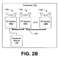
- FIGS. 1, 2A , and 2B are diagrams of transceivers according to various embodiments of the present disclosure.
- FIG. 3 is a diagram illustrating one example of a multiplexed signal present on an interface connecting a baseband module and one or more radio-frequency (RF) modules of the transceiver according to one embodiment.
- RF radio-frequency
- FIG. 4 is block diagram illustrating components of a baseband module and an RF module of the used in modulating and demodulating a control signal of the multiplexed signal in a transceiver according to one embodiment.
- FIG. 5 is a diagram of one example of a packet format employed for control data traffic in a transceiver according to one embodiment.
- FIG. 6 is a diagram of one example of a streaming format that may be employed for automatic gain control (AGC) data traffic in a transceiver according to one embodiment.
- AGC automatic gain control
- FIG. 7 is a diagram of one example configuration of an antenna configuration look-up table employed to configure an antenna array of an RF module in a transceiver according to one embodiment.
- FIG. 8 is a diagram of one example of a beam refinement packet format that may be employed during a beam refinement operation in a transceiver according to one embodiment.
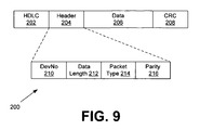
- FIG. 9 is a diagram of one example of a general packet format that may be employed in a transceiver according to one embodiment.
- FIG. 10 is a flowchart illustrating one example of operation of a portion of a transceiver according to various embodiments.
- the transceiver 100 which implements a split architecture interface, includes a baseband module 103 and a radio-frequency (RF) module 106 coupled by way of an interface 109.
- the RF module 106 is coupled to an antenna array 112 including one or more antennas for transmitting and/or receiving an extremely high frequency RF signal such as, for example, a 60 GHz RF signal, a 77 GHz RF signal, 96 GHz RF signal, and/or other extremely high frequency signals that necessitate colocation of the RF module 106 with the antenna array 112.
- an extremely high frequency RF signal such as, for example, a 60 GHz RF signal, a 77 GHz RF signal, 96 GHz RF signal, and/or other extremely high frequency signals that necessitate colocation of the RF module 106 with the antenna array 112.
- the interface 109 may correspond, for example, to a single, shielded coaxial cable interface used to transfer the intermediate frequency (IF) signal, a clock reference, as well as control signals from the baseband module 103 for controlling the operation of the RF module 106.
- IF intermediate frequency
- the interface 109 may correspond, for example, to a single, shielded coaxial cable interface used to transfer the intermediate frequency (IF) signal, a clock reference, as well as control signals from the baseband module 103 for controlling the operation of the RF module 106.
- the antenna array 112 is co-located with the RF module 106 due to the characteristics of the extremely high frequency RF signal being transmitted and/or received. Line loss at frequencies of 60 GHz and upwards may be severe, which motivates placing the antenna array 112 as close to the RF module 106 as practical. To this end, the antenna array 112 may be integrated or collocated with the RF module 106.
- the RF module 106 downconverts the extremely high frequency RF signal to an IF signal that may be transmitted over a shielded coaxial cable. Similarly, in a transmit mode, the RF module 106 may upconvert an IF signal received over the shielded coaxial cable to the extremely high frequency signal for transmission.
- the RF module 106 and the baseband module 103 may each be implemented with respective integrated circuit chips in a transceiver device.
- the transceiver 100 includes one baseband module 103 and a plurality of RF modules 106a, 106b ... 106N coupled by way of an interface 109.
- Each of the RF modules 106 may be coupled to a respective one of a plurality of antenna arrays 112a, 112b ... 112N, which each includes one or more antennas for transmitting and/or receiving an extremely high frequency (EHF) RF signal.
- the plurality of RF modules 106 may be connected to the single baseband module 103, for example, through a tap-off arrangement from a single cable segment as shown in FIG. 2A or through a daisy-chain arrangement with multiple cable segments as shown in FIG. 2B .
- Multiple RF modules 106 may be employed due to the propagation characteristics of EHF signals. Compared with other RF signals, EHF signals are less likely to propagate through various materials and reception depends more on a clear line of sight. If only one RF module 106 with an antenna array 112 were used, it may be in a position that is obscured by an attenuating material. Accordingly, multiple RF modules 106 may be utilized in different locations for antenna diversity. Which one, or ones, of the RF modules 106 is used may depend, for example, on the location of the far end transceiver 100 with which communication is desired.
- the transceiver 100 may correspond to a laptop with an aluminum chassis.
- a first RF module 106 may be located on one side of the laptop screen, and a second RF module 106 may be located on the other side of the laptop screen.
- a far-end transceiver is located behind the screen, one of the RF modules 106 that is located at the back of the screen may be used.
- the other one of the RF modules 106 that is located at the front of the screen may be used.
- the RF modules 106 may be active (i.e., able to receive or transmit) at any particular time.
- the other RF modules 106 may be placed in a standby state.
- an RF module 106 may be configured only to receive commands over the interface 109.
- the RF module 106 may be configured to present sufficiently high impedance to the interface 109 in the 8 GHz region so that a minimum amount of the IF signal is lost. Selection of a particular one of the RF modules 106 may be supported. In some embodiments, multiple RF modules 106 may be active simultaneously.
- Speed and timing accuracy of the RF signaling interface between the baseband module 103 and the RF module 106 may be configured to minimize excess time of the RF module 106 in an active mode. It is desired that the excess time in the active mode is only a small fraction of the overall power consumption of the transceiver 100.
- the baseband module 103 is able to write to control and configuration registers of the RF module 106.
- a register banking structure may be in place in the RF module 106 so that multiple registers are not written during mode transition periods.
- the control of the RF module 106 is configured such that various turnaround times are met.
- the turnaround times may be based on different interframe spacing (IFS) types such as, for example, short interframe spacing (SIFS), reduced interframe spacing (RIFS), arbitration interframe spacing (AIFS), distributed coordination function (DCF) interframe spacing (DIFS), and/or others.
- IFS interframe spacing
- RIFS reduced interframe spacing
- AIFS arbitration interframe spacing
- DCF distributed coordination function interframe spacing
- the turnaround times associated with the WiGig specification are met.
- FIG. 3 is a diagram illustrating one example of a multiplexed signal 130 present on the shielded coaxial cable of the interface 109 according to one embodiment.
- the multiplexed signal 130 may include, for example, a direct current (DC) component, a clock reference signal, a control signal, and an IF signal.
- the DC component may be used to power the RF modules 106 without additional power supply connections.
- the frequency of the IF signal may be chosen based at least in part on the properties of the coaxial interface 109. For example, commonly available shielded coaxial cable may have an acceptable signal loss around 8 GHz, but the signal may drop off precipitously after around 8 GHz. Also, it may be the case that test equipment is more expensive beyond around 8 GHz. Accordingly, a frequency near 8 GHz may be chosen as the IF frequency.
- the phase-locked loop (PLL) reference may be sent from the baseband module 103 to be used as the bit clock for the interface 109.
- the clock reference signal is 270 MHz
- the control signal is 2.64 GHz
- the IF signal is 8.64 GHz.
- the control signal may be selected as a multiple of the reference signal
- the IF signal may be selected as a multiple of the control signal.
- the clock reference signal may be 270 MHz
- the control signal may be 2.7 GHz (10 times 270 MHz)
- the IF signal may be 8.1 GHz (3 times 2.7 GHz).
- the control channel carrier frequency is 0 Hz.
- the control channel carrier frequency may be selected so as not to interfere with either the IF or the RF frequencies. By selecting the frequencies according to harmonic relationships, interference among the signals may be minimized.
- FIG. 4 is a block diagram illustrating components of the baseband module 103 and the RF module 106 used in modulating and demodulating the control signal of the multiplexed signal 130 ( FIG. 3 ) according to one embodiment.
- a modulation stage In the baseband module 103, a modulation stage generates a modulated control signal based at least in part on an internally generated PLL clock reference. Amplitude-shift keying (ASK) modulation may be used to modulate the carrier. A modulation depth of 100% corresponding to on/off keying may be employed. Alternatively, programmable modulation depth may be employed to accommodate issues resulting due to a very large change in signal, such as that resulting from voltage-controlled oscillator (VCO) pulling and other causes.
- VCO voltage-controlled oscillator
- a variable resistor may control the output signal level of the modulation stage, which is then provided to a mixer.
- a carrier signal from a local oscillator is then mixed with the modulated signal, thereby shifting the modulated signal to the desired control RF range.
- the resulting signal may be amplified and sent over the coaxial interface 109 to the RF module 106.
- control signal is amplified and processed by an envelope detector.
- the signal is then processed by a high pass filter and slicer, and then provided to a demodulation stage.
- the demodulation stage uses the clock reference from the interface 109 to demodulate the received control signal.
- ASK modulation may be employed.
- the RF module 106 may generate a carrier suitable for the control signal for other uses and may thus use minimal circuitry to generate its own modulated carrier.
- the RF module 106 may then employ the same modulation and line coding as for the baseband module 103.
- the RF module 106 may, for example, employ a controllable modulation index with a maximum of 100%.
- the read-back function for the RF module 106 may not have timing critical restraints in some cases. Therefore, the data rate for read-back may be significantly reduced.
- the read-back data rate from the RF module 106 may be 67.5 MHz, which corresponds to a 270 MHz reference signal divided by four.
- the RF voltage control oscillator may be divided down to generate a source close in frequency to the control carrier. With amplitude modulation being employed, carrier frequency synchronization may not be required. With such an approach, there may be a need to enable the RF PLL at an appropriate frequency before read-back may be performed.
- carrier offset modulation may be employed.
- the RF module 106 may generate an offset double sideband carrier by mixing the carrier from the baseband module 103 with the clock reference to generate carriers at the control RF carrier signal (e.g., 2700 MHz) plus or minus the clock reference signal (e.g., plus or minus 270 MHz).
- the generated carrier can then be ASK modulated as described in connection with the baseband module 103.
- carrier offset load modulation may be employed.
- the RF module 106 does not otherwise include a local control carrier source, and the cost for generating such a carrier may be significant.
- the modulated signal could be, for example, a 270 MHz Manchester coded signal or a double sideband suppressed carrier signal with carrier at plus or minus 270 MHz modulated by data at a fraction of the 270 MHz rate.
- the composite signal may then be load modulated back to the baseband module 103. This modulation process may be similar to the modulation employed in the 13 MHz RFID and near field communication (NFC) standards of modulation.
- NFC near field communication
- the load modulation process may be a tuned operation such that the modulation process does not affect the main IF signal or the reference signal. If the main IF signal could be affected, then read-back may be limited to occur during silent periods when the main IF carrier is off and the clock reference quality is not critical.
- CDR clock and data recovery
- the packet format 150 includes a preamble field 151, a character delimiter field 153, an address field 155, a data field 157, a cyclic redundancy check (CRC) field 159, and potentially other data.
- the preamble field 151 may contain, for example, alternating 1s and 0s to provide a direct current (DC) free signal for DC removal before the character delimiter field 153.
- the last bit of the preamble field 153 is the inverse of the first bit of the character delimiter field 153.
- the character delimiter field 153 is a predetermined bit sequence that marks the start of a byte stream. If multiple RF modules 106 are coupled to the interface 109, special character delimiters may be used for selection of RF modules 106.
- the address field 155 may contain one or more bytes that indicate a memory mapped address being written or read.
- the data field 157 may include multiple bytes of written data. In a read operation, the data field 157 may be omitted. For a basic write command, the number of bytes may be fixed at a predetermined number.
- the CRC field 159 includes a standard CRC covering the address field 155 and the data field 157. In one embodiment, the CRC is a 16 bit CRC.
- the sections of the transmitted packet format 150 other than the preamble field 151 may be coded using an 8b/10b code or another coding technique.
- These two special characters within the 8b/10b code set may be chosen because they have a unique run of five bits of the same sign that cannot be found in other combinations of coded words, as long as the K28.7 special character is also not used.
- control words as a character delimiter as well as an RF module selection, other control codes could be used. This is because the bits prior to the character delimiter will be "01" or "10" in this example.
- the baseband module 103 may be configured to verify the integrity of a block of multiple write transactions by performing a single read operation.
- the RF module 106 includes a counter that tracks the number of write transaction received, and a counter that tracks the number of write transactions received with a CRC error or other error.
- the baseband module 103 may read these counters to determine whether all write transactions were received by the RF module 106 and to determine whether any of the transactions resulted in an error.
- a read to the counters which may correspond to a single read to a register, may set the counters back to zero.
- the same packet format 150 may be employed for the reverse data link.
- the assignment of character delimiter values may be via selector pins on the chip package of the RF module 106.
- a streaming format 160 that may be employed for automatic gain control (AGC) data traffic on the forward link.
- AGC automatic gain control
- a predetermined maximum transaction time may be employed. For example, 64 symbols or half of the G128 in the short training field (STF) may be adequate.
- STF short training field
- a shortened packet format or a continuous stream of AGC data may be employed to relay AGC data.
- a streaming packet format 160 is proposed, where the RF module 106 is configured for an AGC mode based upon a packet being received to set the RF module 106 into receive mode. Any follow on transaction from setting the receive mode may be in a stream mode. In the stream mode, the next character delimiter field 153 received by the RF module 106 indicates the start of the stream.
- the data received corresponds to codes, for example, in 5b/6b format, which is a subset of the 8b/10b coding.
- the data corresponds to a plurality of AGC words 161 a, 161 b ... 161 N.
- the end of the stream may be indicated, for example, by a series of at least six zeros or six ones, which is a 5b/6b coding violation 163.
- Each AGC word 161 may be coded, for example, as an absolute pointer into a look-up table of the RF module 106 or as a relative step within the look-up table of the RF module 106. Such coding of the AGC words 161 may depend on the size of the look-up table.
- an antenna configuration look-up table 170 employed to configure the antenna array 112 of the RF module 106.
- the WiGig specification defines a maximum of 64 beam configurations for sector-level sweep and beam refinement.
- the antenna configuration look-up table 170 may include sections for beam selection configurations (e.g., 16 configurations), connection-oriented configurations, pseudo-omni configurations, and potentially other configurations.
- an eight-bit pointer is assigned for antenna configuration, assuming fewer than 256 configurations.
- the RF module 106 has 17 antenna paths, which are shared between transmission and reception.
- a phase setting (corresponding to "phi” in FIG. 7 ) and a single-bit antenna selection setting (corresponding to "Act” in FIG. 7 ) may be assigned.
- the antenna selection bit may indicate whether a given antenna will be active or disabled for the given configuration.
- a single register write to the RF module 106 may configure the antenna configuration to be used, the selection of TX or RX mode, the transmitter gain setting, and/or other configuration settings.
- the baseband module 103 In normal packet operation, the baseband module 103 will be measuring the received signal strength during packet reception prior to STF acquisition.
- the total gain that is controllable is a combination of gain stages in the baseband module 103 as well as the RF module 106 gain.
- the baseband module 103 may have to send a gain setting message to the RF module 106.
- the gain setting message is configured to be relatively short such that, for example, 1/3 of the 128 symbol long Golay codes used in the STF are used for the gain change transaction. This translates into a maximum of 25 ns for the gain change transaction.
- the RF module 106 During normal operation, it may be assumed that after a SIFS or DIFS period, the RF module 106 is to be configured to either transmit or receive.
- the control interface may be configured such that the TX/RX configuration can be chosen, the antenna configuration can be selected, and the transmit gain can be specified all in a single transaction.
- the antenna configurations in use for both normal operation and beam refinement protocol are stored within the antenna configuration look-up table 170. Therefore, only the pointer for the look-up table needs to be sent.
- the beam refinement packet format 180 may include a short training field (STF) 181, a channel estimation field (CEF) 183, a header field 185, a data field 187, a plurality of AGC fields 189, a plurality of training period-receive/transmit (TRN-R/T) fields 191, and potentially other data.
- STF short training field
- CEF channel estimation field
- TRN-R/T training period-receive/transmit
- a set of AGC fields 189 within the beam refinement section of the packet are intended to be used by the receiver to determine the best gain control setting for each antenna configuration used in the beam refinement operation.
- Each of the AGC fields 189 may include, for example, four 64-bit Golay codes 193a, 193b, 193c, and 193d.
- the optimum gain for each antenna configuration may be determined. In this case, the gain is adjusted dynamically for each antenna configuration. The gain setting is stored to be reused during the TRN-R/T fields 191. In the second approach, the gain required to receive the antenna configuration with the maximum signal power is determined. In this case, the gain is reduced if any part of the AGC fields 189 goes beyond the desired setting.
- the AGC algorithm may be changed from the normal packet reception mode, where, for example, a maximum of three gain steps are employed within the RF module 106. This is possible because in the TRN-R/T fields 191, 128 bit Golay signals may be received and a processing gain of 21 dB allows for a much lower signal-to-noise ratio at the input to the Golay correlator. Due to uncertainty across the IF interface, it may be assumed that for every section of the AGC field 189 or TRN-R/T field 191 transmitted, an initial number of bits (e.g., 64 bits or some other number) may be corrupted due to the transmission process.
- an initial number of bits e.g., 64 bits or some other number
- the first 64-bit Golay code 193a of every AGC field 189 could be corrupted.
- the TRN-R/T fields 191 five 128-bit Golay codes may be transmitted. The latter four may be used for channel estimation. Alternatively, the middle three 128-bit Golay codes may be used for channel estimation.
- both antenna configuration changes and AGC changes may be occurring in a very tight sequence. This may place stringent timing and packet structure configuration requirements on this operation. This is amplified with the AGC fields 189, where it may be expected that the antenna configuration take less than one 64-bit Golay code 193 signal period. This is equivalent to less than ten bits of data at a 270 MHz clock rate.
- This operation may be under finite state machine (FSM) control, which may be programmed and triggered over the control channel.
- FSM finite state machine
- the packet format 200 includes a high-level data-link control (HDLC) field 202, a header field 204, a data field 206, and a CRC field 208.
- the HDLC field 202 is 7 bits
- the header field 204 is 12 bits
- the CRC field is 10 bits.
- the HDLC field 202 may include a delimiter that includes six or some other number of consecutive ones, followed by a zero. Other patterns may be employed in other embodiments.
- An encoder may be used in the transceiver 100 to ensure that this pattern does not occur, except for the beginning of a packet or on a packet abort. This allows for operations of lower importance to be interrupted when operations of higher importance arise.
- the header field 204 may include several subfields such as, for example, a device number field 210, a data length field 212, a packet type field 214, a parity field 216, and/or other fields.
- the device number field 210 is 3 bits
- the data length field 212 is 4 bits
- the packet type field 214 is 3 bits
- the parity field 216 is 2 bits.
- the device number field 210 may include, for example, a device number for an RF module 106 or a broadcast delimiter for programming some or all RF modules 106 concurrently.
- the data length field 212 provides a data length which may be used to allow for multiple consecutive register reads or writes.
- the packet type field 214 may be used to indicate different packet types specified for different operations including, for example, register read/write access, streaming AGC mode, low-latency write, and/or other operations.
- the parity field 216 may provide protection for the header bits.
- FIG. 10 shown is a flowchart that provides one example of the operation of a portion of the transceiver 100 according to various embodiments. It is understood that the flowchart of FIG. 10 provides merely an example of the many different types of functional arrangements that may be employed to implement the operation of the portion of the transceiver 100 as described herein.
- the transceiver 100 obtains a baseband data signal.
- the transceiver 100 generates a multiplexed signal in a baseband module 103 ( FIG. 1 ).
- the multiplexed signal may include, for example, a direct current component, a clock reference signal at a clock reference frequency, a control signal at a control carrier frequency, an intermediate frequency data signal.
- the direct current component may be used for powering the radio-frequency module 106 ( FIG. 1 ).
- the control signal may encode one or more commands for controlling the operation of the radio-frequency module 106.
- the intermediate frequency data signal corresponds to the data signal at an intermediate frequency.
- the transceiver 100 transmits the multiplexed signal from the baseband module 103 to the radio-frequency module 106 via a single shielded coaxial cable.
- the transceiver 100 decodes the control signal in the radio-frequency module 106. In so doing, the transceiver 100 recovers one or more commands to control the operation of the radio-frequency module 106.
- the commands may adjust an automatic gain control setting, select one or more antennas in an antenna array 112, select one or more of multiple radio-frequency modules 106 to be active, and perform other functions.
- a command may trigger an autonomous finite state machine in the radio-frequency module 106 to adjust an automatic gain control setting.
- the transceiver 100 upconverts the intermediate frequency signal to an extremely high frequency signal in the radio-frequency module 106.
- the transceiver 100 wirelessly transmits the extremely high frequency signal via an antenna array 112 ( FIG. 1 ) collocated in the radio-frequency module 106. Thereafter, the operation of the portion of the transceiver 100 ends.
- the transceiver 100 may perform some of the operations of FIG. 10 in reverse. That is to say, the RF module 106 may receive an extremely high frequency data signal and then downconvert it to an intermediate frequency. The downconverted data signal may be transmitted on the same coaxial cable to the baseband module 103. In addition, parameters stored by the RF module 106 may be read back via the control signal by the baseband module 103.
- the various systems described herein may be embodied in dedicated hardware or a combination of software/general purpose hardware and dedicated hardware. If embodied in dedicated hardware, each can be implemented as a circuit or state machine that employs any one of or a combination of a number of technologies. These technologies may include, but are not limited to, discrete logic circuits having logic gates for implementing various logic functions upon an application of one or more data signals, application specific integrated circuits having appropriate logic gates, or other components, etc. Such technologies are generally well known by those skilled in the art and, consequently, are not described in detail herein.
- each block may represent a module, segment, or portion of code that comprises program instructions to implement the specified logical function(s).
- the program instructions may be embodied in the form of source code that comprises human-readable statements written in a programming language or machine code that comprises numerical instructions recognizable by a suitable execution system such as a processor in a computer system or other system.
- the machine code may be converted from the source code, etc.
- each block may represent a circuit or a number of interconnected circuits to implement the specified logical function(s).
- FIG. 10 shows a specific order of execution, it is understood that the order of execution may differ from that which is depicted. For example, the order of execution of two or more blocks may be scrambled relative to the order shown. Also, two or more blocks shown in succession in FIG. 10 may be executed concurrently or with partial concurrence. Further, in some embodiments, one or more of the blocks shown in FIG. 10 may be skipped or omitted. In addition, any number of counters, state variables, warning semaphores, or messages might be added to the logical flow described herein, for purposes of enhanced utility, accounting, performance measurement, or providing troubleshooting aids, etc. It is understood that all such variations are within the scope of the present disclosure.
- any logic or application described herein that comprises software or code can be embodied in any non-transitory computer-readable medium for use by or in connection with an instruction execution system such as, for example, a processor in a computer system or other system.
- the logic may comprise, for example, statements including instructions and declarations that can be fetched from the computer-readable medium and executed by the instruction execution system.
- a "computer-readable medium" can be any medium that can contain, store, or maintain the logic or application described herein for use by or in connection with the instruction execution system.
- the computer-readable medium can comprise any one of many physical media such as, for example, magnetic, optical, or semiconductor media. More specific examples of a suitable computer-readable medium would include, but are not limited to, magnetic tapes, magnetic floppy diskettes, magnetic hard drives, memory cards, solid-state drives, USB flash drives, or optical discs. Also, the computer-readable medium may be a random access memory (RAM) including, for example, static random access memory (SRAM) and dynamic random access memory (DRAM), or magnetic random access memory (MRAM).
- RAM random access memory
- SRAM static random access memory
- DRAM dynamic random access memory
- MRAM magnetic random access memory
- the computer-readable medium may be a read-only memory (ROM), a programmable read-only memory (PROM), an erasable programmable read-only memory (EPROM), an electrically erasable programmable read-only memory (EEPROM), or other type of memory device.
- ROM read-only memory
- PROM programmable read-only memory
- EPROM erasable programmable read-only memory
- EEPROM electrically erasable programmable read-only memory
Landscapes
- Engineering & Computer Science (AREA)
- Computer Networks & Wireless Communication (AREA)
- Signal Processing (AREA)
- Transceivers (AREA)
- Mobile Radio Communication Systems (AREA)
- Radio Transmission System (AREA)
Applications Claiming Priority (1)
| Application Number | Priority Date | Filing Date | Title |
|---|---|---|---|
| US42102710P | 2010-12-08 | 2010-12-08 |
Publications (2)
| Publication Number | Publication Date |
|---|---|
| EP2544378A2 true EP2544378A2 (de) | 2013-01-09 |
| EP2544378A3 EP2544378A3 (de) | 2014-05-28 |
Family
ID=45372180
Family Applications (1)
| Application Number | Title | Priority Date | Filing Date |
|---|---|---|---|
| EP11009682.3A Withdrawn EP2544378A3 (de) | 2010-12-08 | 2011-12-08 | Verfahren und System für Hochfrequenz-Steuerungsschnittstelle für einen 60-GHz-Chipsatz (HF-Modulsteuerungsschnittstelle) |
Country Status (4)
| Country | Link |
|---|---|
| US (1) | US20120309325A1 (de) |
| EP (1) | EP2544378A3 (de) |
| CN (1) | CN102655418A (de) |
| TW (1) | TW201246816A (de) |
Cited By (4)
| Publication number | Priority date | Publication date | Assignee | Title |
|---|---|---|---|---|
| WO2016081131A1 (en) * | 2014-11-19 | 2016-05-26 | Qualcomm Incorporated | Systems and methods for inductively coupled communications |
| US9564972B2 (en) | 2012-07-02 | 2017-02-07 | Corning Incorporated | Cable for radio frequency communication |
| WO2020036690A1 (en) | 2018-08-14 | 2020-02-20 | Avx Antenna Inc. D/B/A Ethertronics Inc. | Method and system for controlling a modal antenna |
| US11469781B2 (en) | 2019-03-07 | 2022-10-11 | Mediatek Inc. | Method for transferring signals via transmission interface and communications apparatus utilizing the same |
Families Citing this family (42)
| Publication number | Priority date | Publication date | Assignee | Title |
|---|---|---|---|---|
| US8913951B2 (en) * | 2007-09-30 | 2014-12-16 | Broadcom Corporation | Method and system for 60 GHz distributed communication utilizing a mesh network of repeaters |
| EP2344915A4 (de) | 2008-10-09 | 2015-01-21 | Corning Cable Sys Llc | Faseroptischer anschluss mit adaptertafel, die sowohl eingangs- als auch ausgangsfasern von einem optischen teiler unterstützt |
| US9118217B2 (en) * | 2010-09-30 | 2015-08-25 | Broadcom Corporation | Portable computing device with wireless power distribution |
| AU2011317244A1 (en) | 2010-10-19 | 2013-05-23 | Corning Cable Systems Llc | Transition box for multiple dwelling unit fiber optic distribution network |
| US8670322B2 (en) | 2011-06-06 | 2014-03-11 | Wilocity, Ltd. | Single transmission line for connecting radio frequency modules in an electronic device |
| US20120309331A1 (en) * | 2011-06-06 | 2012-12-06 | Wilocity, Ltd. | Modular millimeter-wave radio frequency system |
| US9525439B2 (en) * | 2011-12-06 | 2016-12-20 | Qualcomm Incorporated | Fully integrated millimeter-wave radio frequency system |
| US9219546B2 (en) | 2011-12-12 | 2015-12-22 | Corning Optical Communications LLC | Extremely high frequency (EHF) distributed antenna systems, and related components and methods |
| US9077415B2 (en) * | 2011-12-19 | 2015-07-07 | Samsung Electronics Co., Ltd. | Apparatus and method for reference symbol transmission in an OFDM system |
| JP5974022B2 (ja) * | 2012-02-08 | 2016-08-23 | パナソニック株式会社 | 無線通信装置 |
| US10110307B2 (en) * | 2012-03-02 | 2018-10-23 | Corning Optical Communications LLC | Optical network units (ONUs) for high bandwidth connectivity, and related components and methods |
| WO2014040250A1 (en) * | 2012-09-13 | 2014-03-20 | Telefonaktiebolaget L M Ericsson (Publ) | Method and apparatus for antenna calibration |
| CN107888234B (zh) | 2012-09-14 | 2021-11-30 | 凯萨股份有限公司 | 用于对第一设备主机系统提供应用支持的方法及第一设备 |
| US9143200B2 (en) * | 2012-09-26 | 2015-09-22 | Qualcomm Incorporated | Apparatus and method of receiver architecture and low-complexity decoder for line-coded and amplitude-modulated signal |
| GB2519287A (en) * | 2013-09-26 | 2015-04-22 | Socowave Technologies Ltd | Network element, radio frequency mast-top module and methods therefor |
| JP6587615B2 (ja) * | 2014-01-24 | 2019-10-09 | カリフォルニア インスティチュート オブ テクノロジー | デュアル周波数光源 |
| US20150244548A1 (en) * | 2014-02-27 | 2015-08-27 | Qualcomm Incorporated | Frequency adjustment of signals |
| CN106463843B (zh) * | 2014-05-23 | 2019-12-13 | 华为技术有限公司 | 一种多波束成型装置及基站 |
| TWI528294B (zh) | 2014-06-23 | 2016-04-01 | 啟碁科技股份有限公司 | 射頻辨識讀取裝置 |
| KR102238709B1 (ko) * | 2014-09-12 | 2021-04-12 | 삼성전자주식회사 | 무선 주파수 처리 장치 및 방법 |
| KR102342740B1 (ko) * | 2014-09-15 | 2021-12-23 | 삼성전자주식회사 | 신호 송수신 방법 및 장치 |
| US10784904B2 (en) * | 2015-02-23 | 2020-09-22 | Qualcomm Incorporated | Transceiver configuration for millimeter wave wireless communications |
| US9461716B2 (en) * | 2015-03-02 | 2016-10-04 | Intel IP Corporation | Near field communications (NFC) modulation feedback apparatus for tuned antenna configurations |
| US9667290B2 (en) | 2015-04-17 | 2017-05-30 | Apple Inc. | Electronic device with millimeter wave antennas |
| US9716537B2 (en) * | 2015-04-23 | 2017-07-25 | Nitero Pty Ltd | Automatic antenna sector-level sweep in an IEEE 802.11ad system |
| US9960877B2 (en) * | 2015-04-30 | 2018-05-01 | Inten IP Corporation | Apparatus, system and method of beamforming |
| CA2992289A1 (en) * | 2015-07-22 | 2017-01-26 | Blue Danube Systems, Inc. | A modular phased array |
| US10230433B2 (en) * | 2015-07-27 | 2019-03-12 | Qualcomm Incorporated | Techniques for improving coverage of communication devices |
| US9942060B2 (en) * | 2015-08-01 | 2018-04-10 | Intel IP Corporation | Techniques for performing multiple-input and multiple-output training using a beam refinement packet |
| US9946322B2 (en) | 2016-01-14 | 2018-04-17 | Qualcomm Incorporated | Wake-up detector |
| US9813081B2 (en) * | 2016-02-03 | 2017-11-07 | Qualcomm Incorporated | Over-the-air loopback for array identification |
| US10735838B2 (en) | 2016-11-14 | 2020-08-04 | Corning Optical Communications LLC | Transparent wireless bridges for optical fiber-wireless networks and related methods and systems |
| US10476557B2 (en) * | 2016-12-06 | 2019-11-12 | Qualcomm Incorporated | Efficient control mechanism in distributed antenna modules |
| US10804616B2 (en) * | 2018-03-27 | 2020-10-13 | Viasat, Inc. | Circuit architecture for distributed multiplexed control and element signals for phased array antenna |
| US11108170B2 (en) | 2018-11-01 | 2021-08-31 | Qualcomm Incorporated | Multi-band millimeter-wave (MMW) antenna array and radio-frequency integrated circuit (RFIC) module |
| US10594368B1 (en) * | 2019-01-31 | 2020-03-17 | Capital One Services, Llc | Array and method for improved wireless communication |
| CN112134712B (zh) | 2019-06-25 | 2021-12-31 | 华为技术有限公司 | 一种信号处理方法以及相关设备 |
| KR20210006157A (ko) * | 2019-07-08 | 2021-01-18 | 삼성전자주식회사 | 라디오 주파수 체인들을 이용하여 신호를 처리하는 방법 및 그 전자 장치 |
| US10784568B1 (en) | 2019-11-27 | 2020-09-22 | Rockwell Collins, Inc. | System and method for retrofitting digital antenna arrays |
| CN112134580A (zh) * | 2019-12-17 | 2020-12-25 | 中兴通讯股份有限公司 | 本振控制方法和系统、信号收发方法和终端 |
| US11140633B2 (en) * | 2020-02-10 | 2021-10-05 | Samsung Electronics Co., Ltd. | Method and apparatus for loopback gain step calibration on RF chain with phase shifter |
| CN111988054B (zh) * | 2020-08-28 | 2021-11-05 | 电子科技大学 | 用于接收物联网终端信号的信号接收系统 |
Family Cites Families (19)
| Publication number | Priority date | Publication date | Assignee | Title |
|---|---|---|---|---|
| US4776041A (en) * | 1986-12-04 | 1988-10-04 | The Mitre Corporation | Collision detection in a fiber optic local area network |
| US5519691A (en) * | 1994-06-03 | 1996-05-21 | At&T Corp. | Arrangement for and method of providing radio frequency access to a switching system |
| KR100309748B1 (ko) * | 1997-12-26 | 2001-12-17 | 윤종용 | 상향파일럿신호를이용한케이블에취에프씨망을위한양방향간선증폭기및에취에프씨망의케이블모뎀 |
| JP2002280942A (ja) * | 2001-03-15 | 2002-09-27 | Nec Corp | 可変指向性アンテナを備えた情報端末装置 |
| CA2364133A1 (en) * | 2001-11-28 | 2003-05-28 | Integen Technologies Inc. | Local area and multimedia network using radio frequency transceivers and coaxial cable |
| CN1486035A (zh) * | 2002-09-28 | 2004-03-31 | 深圳市中兴通讯股份有限公司 | 一种无线接入装置 |
| US7280824B2 (en) * | 2003-02-28 | 2007-10-09 | National Institute Of Information And Communications Technology | Wireless communication system |
| WO2004082277A1 (en) * | 2003-03-11 | 2004-09-23 | Thomson Licensing S.A. | Apparatus and method for distributing signals |
| US7366473B2 (en) * | 2004-04-28 | 2008-04-29 | Intel Corporation | Method and apparatus for diversity switching control |
| JP4369335B2 (ja) * | 2004-09-29 | 2009-11-18 | 三菱電機株式会社 | 路側狭域無線通信装置 |
| CN100426897C (zh) * | 2005-01-12 | 2008-10-15 | 华为技术有限公司 | 分体式基站系统及其组网方法和基带单元 |
| CN100375550C (zh) * | 2005-03-07 | 2008-03-12 | 大唐移动通信设备有限公司 | 一种基站系统 |
| US7848770B2 (en) * | 2006-08-29 | 2010-12-07 | Lgc Wireless, Inc. | Distributed antenna communications system and methods of implementing thereof |
| CN101094460A (zh) * | 2007-04-20 | 2007-12-26 | 芯通科技(成都)有限公司 | 使用中频连接的微基站的设计方法和装置 |
| KR100912506B1 (ko) * | 2007-08-28 | 2009-08-17 | 한국전자통신연구원 | 기지국 송수신 안테나 및 그의 운용 방법 |
| US9002300B2 (en) * | 2010-09-30 | 2015-04-07 | Broadcom Corporation | Method and system for time division duplexing (TDD) in a 60 GHZ distributed communication system |
| ES2350542B1 (es) * | 2008-12-12 | 2011-11-16 | Vodafone España, S.A.U. | Sistema y antena para redes de acceso de radio. |
| CN101867402B (zh) * | 2010-05-04 | 2014-01-29 | 西安交通大学 | 一种自适应天线选择的mimo系统及其应用方法 |
| US8670322B2 (en) * | 2011-06-06 | 2014-03-11 | Wilocity, Ltd. | Single transmission line for connecting radio frequency modules in an electronic device |
-
2011
- 2011-12-08 EP EP11009682.3A patent/EP2544378A3/de not_active Withdrawn
- 2011-12-08 CN CN2011104063608A patent/CN102655418A/zh active Pending
- 2011-12-08 US US13/314,277 patent/US20120309325A1/en not_active Abandoned
- 2011-12-08 TW TW100145431A patent/TW201246816A/zh unknown
Non-Patent Citations (1)
| Title |
|---|
| None |
Cited By (9)
| Publication number | Priority date | Publication date | Assignee | Title |
|---|---|---|---|---|
| US9564972B2 (en) | 2012-07-02 | 2017-02-07 | Corning Incorporated | Cable for radio frequency communication |
| WO2016081131A1 (en) * | 2014-11-19 | 2016-05-26 | Qualcomm Incorporated | Systems and methods for inductively coupled communications |
| US9577718B2 (en) | 2014-11-19 | 2017-02-21 | Qualcomm Incorporated | Systems and methods for inductively coupled communications |
| WO2020036690A1 (en) | 2018-08-14 | 2020-02-20 | Avx Antenna Inc. D/B/A Ethertronics Inc. | Method and system for controlling a modal antenna |
| EP3837771A4 (de) * | 2018-08-14 | 2022-05-11 | AVX Antenna, Inc. D/B/A Ethertronics, Inc. | Verfahren und system zur steuerung einer modalen antenne |
| IL280828B1 (en) * | 2018-08-14 | 2023-11-01 | Avx Antenna Inc D/B/A Ethertronics Inc | Method and system for controlling a modal antenna |
| IL280828B2 (en) * | 2018-08-14 | 2024-03-01 | Avx Antenna Inc D/B/A Ethertronics Inc | Method and system for model antenna control |
| US11469781B2 (en) | 2019-03-07 | 2022-10-11 | Mediatek Inc. | Method for transferring signals via transmission interface and communications apparatus utilizing the same |
| US11929767B2 (en) | 2019-03-07 | 2024-03-12 | Mediatek Inc. | Method for transferring signals via transmission interface and communications apparatus utilizing the same |
Also Published As
| Publication number | Publication date |
|---|---|
| TW201246816A (en) | 2012-11-16 |
| CN102655418A (zh) | 2012-09-05 |
| EP2544378A3 (de) | 2014-05-28 |
| US20120309325A1 (en) | 2012-12-06 |
Similar Documents
| Publication | Publication Date | Title |
|---|---|---|
| EP2544378A2 (de) | Verfahren und System für Hochfrequenz-Steuerungsschnittstelle für einen 60-GHz-Chipsatz (HF-Modulsteuerungsschnittstelle) | |
| US20250167818A1 (en) | Time encoded data communication protocol, apparatus and method for generating and receiving a data signal | |
| US11979177B2 (en) | Time encoded data communication protocol, apparatus and method for generating and receiving a data signal | |
| Chen et al. | Reliable and practical Bluetooth backscatter with commodity devices | |
| KR102238709B1 (ko) | 무선 주파수 처리 장치 및 방법 | |
| EP3335365B1 (de) | Verwaltete zeitduplex-basisbandsignalisierung | |
| WO2022212630A1 (en) | Sync scatter low power backscatter wake up receiver | |
| KR102183960B1 (ko) | 빔 정교화 방법 및 통신 장치 | |
| US9596669B2 (en) | Method and apparatus for transmitting data | |
| US6363086B1 (en) | Method for combining signals on a digital interface | |
| CN114221666B (zh) | 多模式时序控制与中频调制信号产生装置 | |
| US9385804B2 (en) | Transmission unit and a method for transmitting data | |
| CN107148756B (zh) | 信号发送/接收方法和装置 | |
| CN209218085U (zh) | 非接触式通信设备 | |
| CN108282871A (zh) | 接收节点、发送节点和传输方法 | |
| US6968279B2 (en) | Apparatus and method for determining a pulse position for a signal encoded by a pulse modulation | |
| CN113810078B (zh) | 通信系统、通信方法及计算机存储介质 | |
| HK1169224A (en) | Rf module control interface | |
| US10171183B2 (en) | Method and system for interference mitigation in wireless communications assemblies | |
| EP1172978B1 (de) | Diversitätsdetektion von PPM-Signalen | |
| KR100762655B1 (ko) | 통신 시스템에서 데이터 전송 장치 및 방법 | |
| CN118524559A (zh) | 数据传输的方法和通信装置 | |
| Galler | SDR-based RFID reader with sub-symbol-synchronization | |
| CN104700127A (zh) | 一种ic卡数据传输方法 |
Legal Events
| Date | Code | Title | Description |
|---|---|---|---|
| PUAI | Public reference made under article 153(3) epc to a published international application that has entered the european phase |
Free format text: ORIGINAL CODE: 0009012 |
|
| 17P | Request for examination filed |
Effective date: 20111208 |
|
| AK | Designated contracting states |
Kind code of ref document: A2 Designated state(s): AL AT BE BG CH CY CZ DE DK EE ES FI FR GB GR HR HU IE IS IT LI LT LU LV MC MK MT NL NO PL PT RO RS SE SI SK SM TR |
|
| AX | Request for extension of the european patent |
Extension state: BA ME |
|
| PUAL | Search report despatched |
Free format text: ORIGINAL CODE: 0009013 |
|
| AK | Designated contracting states |
Kind code of ref document: A3 Designated state(s): AL AT BE BG CH CY CZ DE DK EE ES FI FR GB GR HR HU IE IS IT LI LT LU LV MC MK MT NL NO PL PT RO RS SE SI SK SM TR |
|
| AX | Request for extension of the european patent |
Extension state: BA ME |
|
| RIC1 | Information provided on ipc code assigned before grant |
Ipc: H04B 1/40 20060101AFI20140424BHEP |
|
| 17Q | First examination report despatched |
Effective date: 20140515 |
|
| STAA | Information on the status of an ep patent application or granted ep patent |
Free format text: STATUS: THE APPLICATION IS DEEMED TO BE WITHDRAWN |
|
| 18D | Application deemed to be withdrawn |
Effective date: 20140701 |