EP2544225A1 - Semiconductor device and bonding material for semiconductor device - Google Patents
Semiconductor device and bonding material for semiconductor device Download PDFInfo
- Publication number
- EP2544225A1 EP2544225A1 EP11750546A EP11750546A EP2544225A1 EP 2544225 A1 EP2544225 A1 EP 2544225A1 EP 11750546 A EP11750546 A EP 11750546A EP 11750546 A EP11750546 A EP 11750546A EP 2544225 A1 EP2544225 A1 EP 2544225A1
- Authority
- EP
- European Patent Office
- Prior art keywords
- semiconductor device
- layer
- bonding material
- substrate
- semiconductor
- Prior art date
- Legal status (The legal status is an assumption and is not a legal conclusion. Google has not performed a legal analysis and makes no representation as to the accuracy of the status listed.)
- Withdrawn
Links
Images





Classifications
-
- H—ELECTRICITY
- H10—SEMICONDUCTOR DEVICES; ELECTRIC SOLID-STATE DEVICES NOT OTHERWISE PROVIDED FOR
- H10W—GENERIC PACKAGES, INTERCONNECTIONS, CONNECTORS OR OTHER CONSTRUCTIONAL DETAILS OF DEVICES COVERED BY CLASS H10
- H10W72/00—Interconnections or connectors in packages
- H10W72/071—Connecting or disconnecting
-
- C—CHEMISTRY; METALLURGY
- C22—METALLURGY; FERROUS OR NON-FERROUS ALLOYS; TREATMENT OF ALLOYS OR NON-FERROUS METALS
- C22C—ALLOYS
- C22C18/00—Alloys based on zinc
-
- B—PERFORMING OPERATIONS; TRANSPORTING
- B23—MACHINE TOOLS; METAL-WORKING NOT OTHERWISE PROVIDED FOR
- B23K—SOLDERING OR UNSOLDERING; WELDING; CLADDING OR PLATING BY SOLDERING OR WELDING; CUTTING BY APPLYING HEAT LOCALLY, e.g. FLAME CUTTING; WORKING BY LASER BEAM
- B23K35/00—Rods, electrodes, materials, or media, for use in soldering, welding, or cutting
- B23K35/22—Rods, electrodes, materials, or media, for use in soldering, welding, or cutting characterised by the composition or nature of the material
- B23K35/24—Selection of soldering or welding materials proper
- B23K35/28—Selection of soldering or welding materials proper with the principal constituent melting at less than 950°C
-
- B—PERFORMING OPERATIONS; TRANSPORTING
- B23—MACHINE TOOLS; METAL-WORKING NOT OTHERWISE PROVIDED FOR
- B23K—SOLDERING OR UNSOLDERING; WELDING; CLADDING OR PLATING BY SOLDERING OR WELDING; CUTTING BY APPLYING HEAT LOCALLY, e.g. FLAME CUTTING; WORKING BY LASER BEAM
- B23K35/00—Rods, electrodes, materials, or media, for use in soldering, welding, or cutting
- B23K35/22—Rods, electrodes, materials, or media, for use in soldering, welding, or cutting characterised by the composition or nature of the material
- B23K35/24—Selection of soldering or welding materials proper
- B23K35/28—Selection of soldering or welding materials proper with the principal constituent melting at less than 950°C
- B23K35/282—Zn as the principal constituent
-
- C—CHEMISTRY; METALLURGY
- C23—COATING METALLIC MATERIAL; COATING MATERIAL WITH METALLIC MATERIAL; CHEMICAL SURFACE TREATMENT; DIFFUSION TREATMENT OF METALLIC MATERIAL; COATING BY VACUUM EVAPORATION, BY SPUTTERING, BY ION IMPLANTATION OR BY CHEMICAL VAPOUR DEPOSITION, IN GENERAL; INHIBITING CORROSION OF METALLIC MATERIAL OR INCRUSTATION IN GENERAL
- C23C—COATING METALLIC MATERIAL; COATING MATERIAL WITH METALLIC MATERIAL; SURFACE TREATMENT OF METALLIC MATERIAL BY DIFFUSION INTO THE SURFACE, BY CHEMICAL CONVERSION OR SUBSTITUTION; COATING BY VACUUM EVAPORATION, BY SPUTTERING, BY ION IMPLANTATION OR BY CHEMICAL VAPOUR DEPOSITION, IN GENERAL
- C23C18/00—Chemical coating by decomposition of either liquid compounds or solutions of the coating forming compounds, without leaving reaction products of surface material in the coating; Contact plating
-
- B—PERFORMING OPERATIONS; TRANSPORTING
- B23—MACHINE TOOLS; METAL-WORKING NOT OTHERWISE PROVIDED FOR
- B23K—SOLDERING OR UNSOLDERING; WELDING; CLADDING OR PLATING BY SOLDERING OR WELDING; CUTTING BY APPLYING HEAT LOCALLY, e.g. FLAME CUTTING; WORKING BY LASER BEAM
- B23K2101/00—Articles made by soldering, welding or cutting
- B23K2101/36—Electric or electronic devices
- B23K2101/40—Semiconductor devices
-
- H—ELECTRICITY
- H10—SEMICONDUCTOR DEVICES; ELECTRIC SOLID-STATE DEVICES NOT OTHERWISE PROVIDED FOR
- H10W—GENERIC PACKAGES, INTERCONNECTIONS, CONNECTORS OR OTHER CONSTRUCTIONAL DETAILS OF DEVICES COVERED BY CLASS H10
- H10W72/00—Interconnections or connectors in packages
- H10W72/071—Connecting or disconnecting
- H10W72/073—Connecting or disconnecting of die-attach connectors
-
- H—ELECTRICITY
- H10—SEMICONDUCTOR DEVICES; ELECTRIC SOLID-STATE DEVICES NOT OTHERWISE PROVIDED FOR
- H10W—GENERIC PACKAGES, INTERCONNECTIONS, CONNECTORS OR OTHER CONSTRUCTIONAL DETAILS OF DEVICES COVERED BY CLASS H10
- H10W72/00—Interconnections or connectors in packages
- H10W72/071—Connecting or disconnecting
- H10W72/073—Connecting or disconnecting of die-attach connectors
- H10W72/07351—Connecting or disconnecting of die-attach connectors characterised by changes in properties of the die-attach connectors during connecting
- H10W72/07355—Connecting or disconnecting of die-attach connectors characterised by changes in properties of the die-attach connectors during connecting changes in materials
-
- H—ELECTRICITY
- H10—SEMICONDUCTOR DEVICES; ELECTRIC SOLID-STATE DEVICES NOT OTHERWISE PROVIDED FOR
- H10W—GENERIC PACKAGES, INTERCONNECTIONS, CONNECTORS OR OTHER CONSTRUCTIONAL DETAILS OF DEVICES COVERED BY CLASS H10
- H10W72/00—Interconnections or connectors in packages
- H10W72/30—Die-attach connectors
-
- H—ELECTRICITY
- H10—SEMICONDUCTOR DEVICES; ELECTRIC SOLID-STATE DEVICES NOT OTHERWISE PROVIDED FOR
- H10W—GENERIC PACKAGES, INTERCONNECTIONS, CONNECTORS OR OTHER CONSTRUCTIONAL DETAILS OF DEVICES COVERED BY CLASS H10
- H10W72/00—Interconnections or connectors in packages
- H10W72/30—Die-attach connectors
- H10W72/321—Structures or relative sizes of die-attach connectors
- H10W72/325—Die-attach connectors having a filler embedded in a matrix
-
- H—ELECTRICITY
- H10—SEMICONDUCTOR DEVICES; ELECTRIC SOLID-STATE DEVICES NOT OTHERWISE PROVIDED FOR
- H10W—GENERIC PACKAGES, INTERCONNECTIONS, CONNECTORS OR OTHER CONSTRUCTIONAL DETAILS OF DEVICES COVERED BY CLASS H10
- H10W72/00—Interconnections or connectors in packages
- H10W72/30—Die-attach connectors
- H10W72/351—Materials of die-attach connectors
-
- H—ELECTRICITY
- H10—SEMICONDUCTOR DEVICES; ELECTRIC SOLID-STATE DEVICES NOT OTHERWISE PROVIDED FOR
- H10W—GENERIC PACKAGES, INTERCONNECTIONS, CONNECTORS OR OTHER CONSTRUCTIONAL DETAILS OF DEVICES COVERED BY CLASS H10
- H10W72/00—Interconnections or connectors in packages
- H10W72/30—Die-attach connectors
- H10W72/351—Materials of die-attach connectors
- H10W72/352—Materials of die-attach connectors comprising metals or metalloids, e.g. solders
-
- H—ELECTRICITY
- H10—SEMICONDUCTOR DEVICES; ELECTRIC SOLID-STATE DEVICES NOT OTHERWISE PROVIDED FOR
- H10W—GENERIC PACKAGES, INTERCONNECTIONS, CONNECTORS OR OTHER CONSTRUCTIONAL DETAILS OF DEVICES COVERED BY CLASS H10
- H10W72/00—Interconnections or connectors in packages
- H10W72/30—Die-attach connectors
- H10W72/351—Materials of die-attach connectors
- H10W72/352—Materials of die-attach connectors comprising metals or metalloids, e.g. solders
- H10W72/3528—Intermetallic compounds
-
- H—ELECTRICITY
- H10—SEMICONDUCTOR DEVICES; ELECTRIC SOLID-STATE DEVICES NOT OTHERWISE PROVIDED FOR
- H10W—GENERIC PACKAGES, INTERCONNECTIONS, CONNECTORS OR OTHER CONSTRUCTIONAL DETAILS OF DEVICES COVERED BY CLASS H10
- H10W72/00—Interconnections or connectors in packages
- H10W72/30—Die-attach connectors
- H10W72/351—Materials of die-attach connectors
- H10W72/353—Materials of die-attach connectors not comprising solid metals or solid metalloids, e.g. ceramics
-
- H—ELECTRICITY
- H10—SEMICONDUCTOR DEVICES; ELECTRIC SOLID-STATE DEVICES NOT OTHERWISE PROVIDED FOR
- H10W—GENERIC PACKAGES, INTERCONNECTIONS, CONNECTORS OR OTHER CONSTRUCTIONAL DETAILS OF DEVICES COVERED BY CLASS H10
- H10W72/00—Interconnections or connectors in packages
- H10W72/50—Bond wires
- H10W72/59—Bond pads specially adapted therefor
-
- H—ELECTRICITY
- H10—SEMICONDUCTOR DEVICES; ELECTRIC SOLID-STATE DEVICES NOT OTHERWISE PROVIDED FOR
- H10W—GENERIC PACKAGES, INTERCONNECTIONS, CONNECTORS OR OTHER CONSTRUCTIONAL DETAILS OF DEVICES COVERED BY CLASS H10
- H10W72/00—Interconnections or connectors in packages
- H10W72/90—Bond pads, in general
- H10W72/921—Structures or relative sizes of bond pads
- H10W72/923—Bond pads having multiple stacked layers
-
- H—ELECTRICITY
- H10—SEMICONDUCTOR DEVICES; ELECTRIC SOLID-STATE DEVICES NOT OTHERWISE PROVIDED FOR
- H10W—GENERIC PACKAGES, INTERCONNECTIONS, CONNECTORS OR OTHER CONSTRUCTIONAL DETAILS OF DEVICES COVERED BY CLASS H10
- H10W72/00—Interconnections or connectors in packages
- H10W72/90—Bond pads, in general
- H10W72/951—Materials of bond pads
- H10W72/952—Materials of bond pads comprising metals or metalloids, e.g. PbSn, Ag or Cu
-
- H—ELECTRICITY
- H10—SEMICONDUCTOR DEVICES; ELECTRIC SOLID-STATE DEVICES NOT OTHERWISE PROVIDED FOR
- H10W—GENERIC PACKAGES, INTERCONNECTIONS, CONNECTORS OR OTHER CONSTRUCTIONAL DETAILS OF DEVICES COVERED BY CLASS H10
- H10W90/00—Package configurations
- H10W90/701—Package configurations characterised by the relative positions of pads or connectors relative to package parts
- H10W90/731—Package configurations characterised by the relative positions of pads or connectors relative to package parts of die-attach connectors
- H10W90/734—Package configurations characterised by the relative positions of pads or connectors relative to package parts of die-attach connectors between a chip and a stacked insulating package substrate, interposer or RDL
Definitions
- the present invention relates to semiconductor devices in which a semiconductor member is stacked on a substrate and a semiconductor device bonding materials for bonding a semiconductor member and a substrate together.
- Patent Literature 1 discloses a semiconductor device in which a semiconductor element is die attached to a die pad.
- lead having a low melting point is used as a main component of a bonding material.
- power modules used in hybrid automobiles generate heat in their devices themselves by large current. Further, the modules are located near the engines. Thus, the modules undergo severe temperature environment. Therefore, the bonding material is inferior in thermal stability as and cannot be used as a bonding material for die attachment of next-generation power semiconductors (SiC semiconductor chips) that are assumed to be used under high temperatures of 200°C or higher.
- SiC semiconductor chips next-generation power semiconductors
- the present invention has its object of providing a compound semiconductor device, such as of a GaN semiconductor, a SiC semiconductor, etc. developed as a next-generation power semiconductor and a semiconductor device bonding material excellent in thermal stability as a bonding material for die attaching of a semiconductor device.
- a compound semiconductor device such as of a GaN semiconductor, a SiC semiconductor, etc. developed as a next-generation power semiconductor and a semiconductor device bonding material excellent in thermal stability as a bonding material for die attaching of a semiconductor device.
- a semiconductor device is characterized by including a substrate and a semiconductor member stacked on the substrate, wherein the semiconductor member and the substrate are bonded together by means of a semiconductor device bonding material of which main component is zinc.
- the conventional semiconductor devices use the semiconductor device bonding materials of which main component is lead.
- the semiconductor device bonding materials have low melting points. Therefore, the bonding materials are inferior in thermal stability as and cannot be used as a bonding material for die attachment of the GaN semiconductors and the SiC semiconductors developed as the next-generation power semiconductors that are assumed to be used under high temperatures of 200°C or higher.
- the semiconductor device according to the present invention uses the semiconductor device bonding material of which main component is zinc having a melting point of 420°C. This can obtain a next-generation power semiconductor device excellent in thermal fatigue resistance that can withstand temperature cycles up to 300°C.
- a coating layer to prevent diffusion of the semiconductor device bonding material is provided on at least one of the surface of the substrate and the surface of the semiconductor member. Accordingly, a reaction between the substrate and the semiconductor device bonding material and/or a reaction between the semiconductor member and the semiconductor device bonding material can be inhibited to prevent formation of a reaction layer with less strength. As a result, the bonding strength between the substrate and the semiconductor device bonding material and/or the bonding strength between the semiconductor member and the semiconductor device bonding material can be maintained, thereby obtaining a more reliable semiconductor device.
- the coating layer is configured such that a barrier layer composed of nitride, carbide, or carbonitirde and a protective layer composed of a noble metal are stacked.
- the barrier layer provided, the semiconductor device bonding material can be prevented from diffusing into the substrate.
- noble metals especially, Au
- Au can improve the wettability of the semiconductor device bonding material with respect to the coating layer. This can achieve favorable bonding between the semiconductor device bonding material and the substrate.
- the nitride, the carbide, or the carbonitride composing the barrier layer is selected so as to have free energy smaller than that of a material composing an insulating layer provided in the substrate. Accordingly, activation of the barrier layer can be suppressed to prevent the material composing the substrate or the semiconductor member from moving toward the semiconductor device bonding material. This can inhibit the reaction between the substrate and the semiconductor device bonding material and the reaction between the semiconductor member and the semiconductor device bonding material, thereby preventing formation of a reaction layer with less strength. As a result, a highly reliable semiconductor device can be obtained.
- a material composing the barrier layer is TiN
- a material composing the protective layer is Au, Ag, Cu, Ni, or Pd
- a material composing the insulating layer included in the substrate is Si 3 N 4 , Al 2 O 3 , or AlN.
- TiN as a material composing the barrier layer has free energy smaller than Si 3 N 4 as a material composing the insulating layer included in the substrate.
- the bonding force between Ti and N is larger than that between Ti and Zn and that between N and Zn. Accordingly, the reaction between the substrate and the semiconductor device bonding material can be inhibited, thereby preventing formation of a reaction layer with less strength.
- the zinc has a purity of 90 wt % or higher.
- Zinc is a metal excellent in flexibility and conductivity. Accordingly, when 90 wt % or higher of zinc is contained in the semiconductor device bonding material, breakdown, which is caused due to a shock by bending, folding, or the like a semiconductor device, can be prevented. It is preferable that the zinc has a purity of 99.9999 wt % or higher. The use of highly pure zinc can increase the elongation of the semiconductor device bonding material.
- the barrier layer has a thickness in the range from 100 nm to 2000 nm, and the protective layer has a thickness in the range from 20 nm to 500 nm.
- the barrier layer can sufficiently prevent diffusion of the semiconductor device bonding material, and the protective layer can reliably prevent oxidation and contamination of the semiconductor device bonding material.
- the semiconductor device bonding material contains an additive element.
- the additive element contained, the characteristics of the semiconductor device bonding material can be improved.
- the additive element includes at least one element selected from the group consisting of Ca, Mn, Ti, Cr, Ni, V, and Nb. With such an additive element added, the semiconductor device bonding material can be increased in ductility and can be prevented from being oxidized.
- a semiconductor device bonding material according to the present invention is characterized by bonding the semiconductor member and the substrate together and including zinc as a main component.
- the semiconductor device bonding material of the present invention is a semiconductor device bonding material of which main component is zinc having a melting point of 420°C, the use of the semiconductor device bonding material can obtain a next-generation power semiconductor device excellent in thermal fatigue resistance that can withstand temperature cycles up to 300°C.
- Embodiments of a semiconductor device and a semiconductor device bonding material according to the present invention will be described with reference to FIGS. 1 and 2 . Then, examples of the present invention will be described with reference to FIGS. 3-14 . It is noted that the present invention is not limited to the following embodiments.
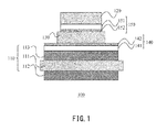
- FIG. 1 is a schematic illustration showing a semiconductor device 100 according to one embodiment of the present invention.
- the semiconductor device 100 has a configuration in which a semiconductor member 120 is stacked on a substrate 110.
- the substrate 110 and the semiconductor member 120 are bonded together by means of a semiconductor device bonding material 130, of which main component is zinc.
- the semiconductor device bonding material 130 is used as a die attaching material (material for die bonding of semiconductor) in semiconductor manufacturing processes. It is a bond in the form of a thin film layer, paste, a film, or the like to bond a semiconductor member (e.g., a die chip) and a substrate together. Since the material of which main component is zinc has a melting point of about 420°C, it may not be melted even at high temperatures around 300°C, thereby exhibiting a function as a die attaching material (material for die bonding of semiconductor).
- the substrate 110 includes an insulating layer 111 and Cu layers (a first Cu layer 112 and a second Cu layer 113) bonded on the opposite surfaces of the insulating layer 111.
- a first coating layer 140 to prevent diffusion of the semiconductor device bonding material 130 is provided on a surface of the substrate 110.
- the first coating layer 140 is configured such that a first barrier layer 141 composed of nitride, carbide, or carbonitride and a first protective layer 142 composed of a noble metal are stacked.
- a second coating layer 150 to prevent diffusion of the semiconductor device bonding material 130 is provided on a surface of the semiconductor member 120.
- the second coating layer 150 is configured such that a second barrier layer 151 composed of nitride, carbide, or carbonitride and a second protective layer 152 composed of a noble metal are stacked.
- the material composing the semiconductor member 120 may be SiC, for example, to allow the semiconductor device 100 to function as an SiC semiconductor device.
- the material composing the semiconductor member 120 may be GaN to allow the semiconductor device 100 to function as a GaN semiconductor device.
- the material composing the insulating layer 111 may be, for example, Si 3 N 4 , but is not limited to Si 3 N 4 as long as the insulating layer 111 can function as an insulator.
- the insulating layer 111 may be composed of Al 2 O 3 or AlN.
- the insulating layer 111 may be composed of another ceramics.
- each thickness of the first protective layer 142 and the second protective layer 152 is in its extent ranging approximately from 20 nm to 500 nm.
- Each of the first protective layer 142 and the second protective layer 152 is composed of a noble metal.
- the noble metal Au, Ag, Cu, Ni, or Pd can be employed, for example.
- the noble metal of Au, Ag, Cu, Ni, and Pd can ensure the wettability of the semiconductor device bonding material 130 to prevent contamination of the semiconductor device bonding material. Provision of an Au layer, an Ag layer, a Cu layer, an Ni layer, or a Pd layer at the bonding interface to the semiconductor device bonding material 130 can prevent void formation at the bonding interface, thereby obtaining a favorable bonding interface.
- each thickness of the first barrier layer 141 and the second barrier layer 151 is in its extent ranging approximately from 100 nm to 2000 nm. With each thickness of the barrier layers 141, 151 falling in this range, the barrier layers 141, 151 can sufficiently prevent diffusion of the semiconductor device bonding material 130. Any of the nitride, carbide, and carbonitride composing the first barrier layer 141 and the second barrier layer 151 is selected so as to have free energy smaller than that of the material composing the insulating layer 111. This can suppress activation of each barrier layer 141, 151 to prevent the material composing the substrate 110 or the semiconductor member 120 from moving toward the semiconductor device bonding material 130.
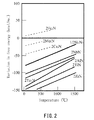
- FIG. 2 is a graph representation showing each variation in free energy of various nitrides.
- the axis of ordinate indicates variation (kcal/mol) in free energy in a reaction (Me + N 2 ⁇ Me-nitride).
- the axis of abscissa indicates temperature (°C).
- NbN, TiN, Ta 2 N, and ZrN are smaller in variation in free energy in the reaction than Si 3 N 4 .
- the material composing the insulating layer is Si 3 N 4
- TiN can be selected as a material composing the first barrier layer 141 and the second barrier layer 151.
- the free energy of TiN is smaller than that of Si 3 N 4 .
- NbN, TiN, Ta 2 N, and ZrN can be used as the material composing the first barrier layer 141 and the second barrier layer 151.
- the material composing the first barrier layer 141 and the second barrier layer 151 is carbide, TiC, TaC, ZrC, NbC, and the like may be used, for example.
- the first barrier layer 141 and the second barrier layer 151 composed of TiC or NbC may be formed in such a manner that after the first barrier layer 141 and the second barrier layer 151 composed of Ti or Nb are formed in advance, SiC composing the semiconductor member 120 is allowed to react with Ti or Nb to change the material composing the first barrier layer 141 and the second barrier layer 151 to TiC or NbC.
- This reaction may be caused in a solid phase. While, solving a metal barrier (e.g., Ti) into the liquid can readily cause the reaction with SiC.
- a metal barrier e.g., Ti
- the material composing the first barrier layer 141 and the second barrier layer 151 may be carbonitride, such as TiCN. It is noted that the first barrier layer 141 and the second barrier layer 151 may be composed of materials different from each other.
- the substrate 110 and the semiconductor member 120 are bonded together by means of the semiconductor device bonding material 130 of which main component is zinc in the semiconductor device 100, the substrate 110 is not limited to having the first coating layer 140 on the surface thereof.
- the semiconductor member 120 is not limited to having the second coating layer 150 on the surface thereof.
- the first coating layer 140 may not be provided on the surface of the substrate 110.
- the second coating layer 150 may not be provided on the surface of the semiconductor member 120.
- each of the first protective layer 142 and the second protective layer 152 is not limited to being a single layer of a noble metal as long as a noble metal layer is provided on the bonding interfaces to the semiconductor device bonding material 130. At least one of the first protective layer 142 and the second protective layer 152 can have at least one metal layer in addition to a single layer of a noble metal. Further, each of the first protective layer 142 and the second protective layer 152 can include a plurality of noble metal layers, such as a noble metal layer including, for example, an Ni layer and an Au layer. Furthermore, a trace amount of an additive can be added to the semiconductor device bonding material 130 when the main component of the material 130 is zinc. The purity of zinc as the main component of the semiconductor device bonding material 130 is 90 wt% or higher, and preferably high purity (99.99 wt % or higher).
- the semiconductor device bonding material of which main component is zinc having a melting point of 420°C is used.
- a next-generation power semiconductor device excellent in thermal fatigue resistance that can withstand temperature cycles up to 300°C can be obtained.
- the coating layer to prevent diffusion of the semiconductor device bonding material is provided on the surface of the substrate. This can inhibit the reaction between the substrate and the semiconductor device bonding material, thereby preventing formation of a reaction layer with less strength. As a result, the bonding strength between the substrate and the semiconductor device bonding material can be maintained, thereby obtaining a highly reliable semiconductor device.
- TiN as a material composing the barrier layers Au, Ag, Cu, Ni, or Pd as a material composing the protective layers, and Si 3 N 4 , Al 2 O 3 , or AlN as a material composing the insulating layer included in the substrate can compose a favorable semiconductor device according to the present invention.
- TiN as a material composing the barrier layers has free energy smaller than Si 3 N 4 as a material composing the insulating layer included in the substrate.
- the bonding force between Ti and N is stronger than that between Ti and Zn and that between N and Zn. Accordingly, the reaction between the substrate and the semiconductor device bonding material can be inhibited to prevent formation of a reaction layer with less strength.
- a highly reliable semiconductor device can be obtained.
- Au, Ag, Cu, Ni, and Pd as materials composing the protective layers can improve the wettability of the semiconductor device bonding material with respect to the coating layers. Accordingly, when an Au layer, an Ag layer, a Cu layer, an Ni layer, or a Pd layer is provided on the bonding interfaces to the semiconductor device bonding material, void formation at the bonding interfaces can be prevented to obtain an excellent bonding interfaces.
- the additive element includes at least one element selected from the group consisting of, for example, Ca (calcium), Mn (manganese), Ti (titanium), Cr (chromium), Ni (nickel) , V (vanadium), and Nb (niobium).
- Ca is an alkaline-earth metal
- Mn, Ti, Cr, Ni, V, and Nb are transition metals.
- Ni, V, and Nb are also called high melting point metals.
- Addition of such an additive element can improve the ductility of the semiconductor device bonding material 130 and can reduce oxidation of the semiconductor device bonding material 130. It is considered that when an element that tends to be oxidized more easily than zinc is used as an additive element, an oxide film serving as a protective film for zinc might be formed on the surface of the semiconductor device bonding material 130. Further, the use of highly pure zinc in the semiconductor device bonding material 130 can improve the ductility.
- a sample 1 for a thermal shock test a sample 1 for a thermal shock test, a sample 2 for a thermal shock test, and a comparative sample for a thermal shock test were prepared.
- pure zinc (a purity of 99.99 wt %, 4 mm long, 4 mm wide, and 0.2 mm thick) was used as the semiconductor device bonding material 130.
- As the insulating layer 111 an Si 3 N 4 layer (15 mm long, 15 mm wide, and 0.5 thick) was used.
- An Au layer (13 mm long, 13 mm wide, and 200 nm thick) as the first protective layer 142 and a TiN layer (13 mm long, 13 mm wide, and 800 nm thick) as the first barrier layer 141 were formed on one surface of the substrate 100 (the second Cu layer 113 (13 mm long, 13 mm wide, and 0.5 mm thick)).
- the Au layer was stacked on the side of the semiconductor device bonding material 130, and the TiN layer was stacked on the side of the second Cu layer 113.
- An Au layer (3 mm long, 3 mm wide, and 200 nm thick) as the second protective layer 152 and a TiN layer (3 mm long, 3mm wide, and 800 nm thick) as the second barrier layer 151 were formed on one surface of the semiconductor member 120 (3 mm long, 3 mm wide, and 1 mm thick).
- the Au layer is stacked on the side of the semiconductor device bonding material 130, and the TiN layer is stacked on the side of the semiconductor member 120.
- the sample 2 for a thermal shock test includes, of the layers of the sample 1 for a thermal shock test, the layers other than the first coating layer 140.
- the comparative sample for a thermal shock test has the same configuration as the sample 1 for a thermal shock test except that Pb-5Sn having a melting point of 315°C was used as the semiconductor device bonding material.
- Each of the thermal shock test sample 1 and the thermal shock test comparative sample was prepared by polishing the surface of the first Cu layer and vapor depositing the first coating layer.
- Each semiconductor device bonding material of the thermal shock test sample 1, the thermal shock test sample 2, and the thermal shock test comparative sample was melted by an infrared furnace (under an Ar atmosphere at a temperature of 450°C for 60 seconds (melting point of 420°C or higher for 100 seconds)).
- a temperature cycle (0-500 times) between -50°C and 300°C in the air was performed on each of the thermal shock test sample 1, the thermal shock test sample 2, and the thermal shock test comparative sample. In each cycle, the samples were held for 30 minutes.
- FIG. 3 is a photo showing a cross section of the thermal shock test sample 1 after the thermal shock test.
- the thermal shock test sample 1 after the thermal shock test includes an SiC layer (the semiconductor member 120), a TiN layer (the second barrier layer 151), a Zn layer (the semiconductor device bonding material 130), and a Cu layer (the second Cu layer 113). Both the bonding interface between the semiconductor member 120 and the semiconductor device bonding material 130 and the bonding interface between the substrate 110 and the semiconductor device bonding material 130 were thoroughly wet, and no void could be found.
- An AuZn compound was recognized inside the Zn layer (the semiconductor device bonding material 130), of which amount is too small to be determined ((18-22 at %) Au to (78-82 at %) Zn).
- FIG. 4 is a photo showing a cross section of the thermal shock test sample 2 after the thermal shock test.
- the thermal shock test sample 2 after the thermal shock test includes an SiC layer (the semiconductor member 120), a TiN layer (the second barrier layer 151), a Zn layer (the semiconductor device bonding material 130), a CuZn 5 layer, a Cu 5 Zn 8 layer, and a Cu layer (the second Cu layer 113).
- the Zn layer the semiconductor device bonding material 130
- the Cu layer the semiconductor device bonding material 130
- FIG. 5 is a photo showing a cross section of the thermal shock test comparative sample after the thermal shock test.
- the thermal shock test comparative sample after the thermal shock test includes an SiC layer, a TiN layer, a Pb-5Sn layer (the semiconductor device bonding material), and a Cu layer. Cracks run inside the Pb-5Sb layer (the semiconductor device bonding material)
- FIG. 6 explains the configuration of a shear test sample and the results of a shear test.
- FIG. 6A is a schematic illustration showing the configuration of the shear test sample.
- a shear test sample 1 For the shear test, a shear test sample 1, a shear test sample 2, and a shear test comparative sample were prepared.
- Each of the shear test sample 1 and the shear test comparative sample includes, in this order from the bottom, a first Cu layer 213 (7 mm long, 11 mm wide, and 0.8 mm thick), a first coating layer 240 (including an Au layer 242 with a thickness of 200 nm and a TiN layer 241 with a thickness of 800 nm), a semiconductor device bonding material layer 230 (4 mm long, 4 mm wide, and 0.2 mm thick), a second coating layer 250 (including an Au layer 252 with a thickness of 200 nm and a TiN layer 251 with a thickness of 800 nm), and a second Cu layer 220 (4 mm long, 4 mm wide, and 0.8 mm thick).
- the shear test sample 2 includes, of the layers of the shear test sample 1, the layers other than the first coating layer 240.
- the semiconductor device bonding material of the shear test sample 1 and the shear test sample 2 is pure zinc (a purity of 99.99 wt %).
- the semiconductor device bonding material of the shear test comparative sample is Pb-5Sn.
- each of the shear test sample 1, the shear test sample 2, and the shear test comparative sample was subjected to a temperature cycle (0-500 times) between -50°C and 300°C in the air. In each cycle, the samples were held for 30 minutes. In each of 0th, 250 th , and 500 th temperature cycles, a shock by a head was provided.
- the test height (position of the head) was 0.1 mm above the upper surface of the first coating layer 240.
- the test speed (head speed) was 50 ⁇ m/s.
- the location at which shear force was provided (part of the semiconductor device bonding material layer 230) is indicted by an arrow in FIG. 6A .
- FIG. 6B is a graph representation showing the results of the shear test obtained from the shear test sample 1, the shear test sample 2, and the shear test comparative sample.
- the axis of ordinate indicates shear strength (MPa).
- the axis of abscissa indicates the number (times) of the temperature cycles.
- the shear test sample 1 exhibited a shear strength of about 36 to 39 MPa, which was about 3.5 times that of the shear test comparative sample.
- the semiconductor device bonding material of which main component is zinc having a melting point of 420°C is used. This can obtain a next-generation power semiconductor device excellent in thermal fatigue resistance that can withstand temperature cycles up to 300°C.
- samples 1-5 were prepared.
- Commercially available zinc to which no additive element is added was prepared as the sample 1.
- the purity of this zinc was 99.99 wt %.
- Such zinc is expressed as 4N.
- zinc to which no additive element is added in the sample 1 may be called pure zinc.
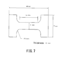
- FIG.7 is a schematic illustration of a test piece. Specifically, the samples 1-5 were casted and rolled so as to reduce their thickness from 10-13 mm to 1.3 mm. Thereafter, electrical discharge machining was performed. Thus, the sample pieces 1-5 were formed from the samples 1-5, respectively.
- test pieces 1-5 were subjected to polishing so as to have a thickness of 1.2 mm and then subjected to thermal treatment at a temperature of 180°C for three hours to remove residual stress. Thereafter, each test piece 1-5 was subjected to polishing with an alumina abrasive. In the polishing, the grain diameter of the alumina abrasive was reduced gradually, and the abrasive having a grain diameter of 0.3 ⁇ m was used at the final stage.
- test pieces 1-5 Ten pieces for each of the test pieces 1-5 were prepared by the above described manner. Then, a tensile test was performed thereon. The extension rate was 7x10 -4 mm/sec. It is noted that any test pieces that were broken at their parts other than the gage length in the tensile test were ignored. Further, of the results of the remaining test pieces, the averages of each six results of the remaining test pieces except the maximum values and the minimum values were calculated.
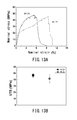
- FIG. 8 presents the results of the tensile test.
- FIG. 8A indicates nominal stress with respect to nominal strain.
- FIG. 8B shows ultimate tensile stress (UTS) of each of the test pieces 1-5.
- UTS ultimate tensile stress
- the results of the test pieces 1-5 are indicated by Zn, 0.1Ca, 0.1Mn, O.lCr, and 0.1Ti, respectively.
- Addition of Ca, Mn, Cr, or Ti expanded the elastic ranges and increased the Young's moduli. Especially, addition of Ti significantly increased the Young's module.
- FIG. 9A shows elongation as the results obtained from the test pieces 1-5. While the test piece 1 had a comparatively low elongation, 5.0 %, the test pieces 2-4 to which the respective additive elements were added showed elongations of 20 % or higher. Thus, it was found that addition of the additive elements increases the elongation.
- FIG. 9B shows the results of 0.2 % proof strength.
- the sample 4 to which Cr was added had almost equivalent proof strength to that of the sample 1.
- the semiconductor device bonding material is composed of a material having less proof strength as the sample 4 than that of the samples 2, 3, and 5, the semiconductor device can absorb damage to the semiconductor member when the semiconductor device receives a shock.
- FIG. 10 presents enlarged images of the samples 1-5.
- FIGS. 10A-10E are images of the samples 1-5, respectively.
- the crystal grains of zinc in the sample 1 were comparatively large.
- addition of the respective additive elements reduced the grain diameters of the zinc crystals.
- the samples 4 and 5, to which Cr and Ti were added, respectively, were reduced in grain diameter of the zinc crystals.
- FIGS. 11A and 11B show enlarged images of the respective broken-out sections in the initial structures of the sample 5 to which Ti was added and the sample 1, respectively. Part that seems an intra-metal compound was observed in the sample 5.
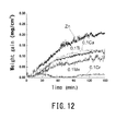
- FIG. 12 shows the results of weight gains of the samples 1-5 depending on oxidation time.
- the weight gain of the sample 1 depending on oxidation time was comparatively large.
- addition of the respective additive elements resulted in comparatively small weight gains depending on the oxidation time in the samples 2-5.
- addition of Cr significantly reduced the weight gain.
- addition of the respective additive elements could suppress oxidation of the samples of which main component is zinc.
- zinc having a purity of 99.99 wt % (4N) and zinc having a purity of 99.9999 wt % were compared with each other. It is noted that the characteristics of the zinc (4N) having a purity of 99.99 wt % are the same as that having the results described with reference to FIGS. 8 and 9 .
- the zinc having a purity of 99.9999 wt % was prepared as a sample 6 herein. This zinc is expressed as 6N.
- the sample 6 was rolled to reduce its thickness from 10-13 mm to 1.3 mm and then was subjected to electrical discharge machining to have a shape shown in FIG. 7 . Thus, a sample piece 6 was formed from the sample 6.
- test piece 6 was subjected to polishing so as to have a thickness of 1.2 mm and then subjected to thermal treatment at a temperature of 180°C for three hours to remove residual stress. Thereafter, the test piece 6 was subjected to polishing with an alumina abrasive. In the polishing, the grain diameter of the alumina abrasive was reduced gradually, and the abrasive having a grain diameter of 0.3 ⁇ m was used at the final stage. Three test pieces 6 were prepared by the foregoing manner. Then, the tensile test was performed thereon. The extension rate was 7x10 -4 mm/sec.
- FIG. 13 presents the results of the tensile test.
- FIG. 13A indicates nominal stress with respect to nominal strain.
- FIG. 13B shows ultimate tensile stress (UTS) of each of the test pieces 1 and 6.
- UTS ultimate tensile stress
- FIGS. 13A and 13B the results of the test pieces 1 and 6 are indicated by 4NZn and 6NZn, respectively.
- the elastic range expanded As the purity of zinc increased, the elastic range expanded.
- FIG. 14A shows elongation as the results of each of the test pieces 1 and 6.
- the elongation of the test piece 1 was comparatively low, 5.0 %.
- the elongation of the test piece 6 was over 8 % Thus, as the purity of zinc increased, the elongation increased.
- FIG. 14B shows the results of 0.2 % proof strength. Increase in purity of zinc accompanied reduction in proof strength.
- the semiconductor device and the semiconductor device bonding material according to the present invention are applicable to compound semiconductor devices, such as GaN semiconductor devices, SiC semiconductor devices, etc. developed as next-generation power semiconductors.
Landscapes
- Chemical & Material Sciences (AREA)
- Engineering & Computer Science (AREA)
- Mechanical Engineering (AREA)
- Materials Engineering (AREA)
- Metallurgy (AREA)
- Organic Chemistry (AREA)
- General Chemical & Material Sciences (AREA)
- Chemical Kinetics & Catalysis (AREA)
- Die Bonding (AREA)
Abstract
Description
- The present invention relates to semiconductor devices in which a semiconductor member is stacked on a substrate and a semiconductor device bonding materials for bonding a semiconductor member and a substrate together.
- In general, dies (semiconductor elements) and substrates are bonded together with bonding materials in semiconductor packaging processes. For example,
Patent Literature 1 discloses a semiconductor device in which a semiconductor element is die attached to a die pad. - [PTL 1] Japanese Patent Application Laid-Open Publication No.
6-163737 - Incidentally, in the semiconductor device of PLT1, lead having a low melting point is used as a main component of a bonding material. For example, power modules used in hybrid automobiles generate heat in their devices themselves by large current. Further, the modules are located near the engines. Thus, the modules undergo severe temperature environment. Therefore, the bonding material is inferior in thermal stability as and cannot be used as a bonding material for die attachment of next-generation power semiconductors (SiC semiconductor chips) that are assumed to be used under high temperatures of 200°C or higher.
- The present invention has its object of providing a compound semiconductor device, such as of a GaN semiconductor, a SiC semiconductor, etc. developed as a next-generation power semiconductor and a semiconductor device bonding material excellent in thermal stability as a bonding material for die attaching of a semiconductor device.
- To solve the above problems, a semiconductor device according to the present invention is characterized by including a substrate and a semiconductor member stacked on the substrate, wherein the semiconductor member and the substrate are bonded together by means of a semiconductor device bonding material of which main component is zinc.
- As described in BACKGROUND ART, in order to bond a semiconductor member to a substrate, the conventional semiconductor devices use the semiconductor device bonding materials of which main component is lead. However, the semiconductor device bonding materials have low melting points. Therefore, the bonding materials are inferior in thermal stability as and cannot be used as a bonding material for die attachment of the GaN semiconductors and the SiC semiconductors developed as the next-generation power semiconductors that are assumed to be used under high temperatures of 200°C or higher. By contrast, the semiconductor device according to the present invention uses the semiconductor device bonding material of which main component is zinc having a melting point of 420°C. This can obtain a next-generation power semiconductor device excellent in thermal fatigue resistance that can withstand temperature cycles up to 300°C.
- According to one preferred aspect of the semiconductor device of the present invention, a coating layer to prevent diffusion of the semiconductor device bonding material is provided on at least one of the surface of the substrate and the surface of the semiconductor member. Accordingly, a reaction between the substrate and the semiconductor device bonding material and/or a reaction between the semiconductor member and the semiconductor device bonding material can be inhibited to prevent formation of a reaction layer with less strength. As a result, the bonding strength between the substrate and the semiconductor device bonding material and/or the bonding strength between the semiconductor member and the semiconductor device bonding material can be maintained, thereby obtaining a more reliable semiconductor device.
- According to one preferred aspect of the semiconductor device of the present invention, the coating layer is configured such that a barrier layer composed of nitride, carbide, or carbonitirde and a protective layer composed of a noble metal are stacked. With the barrier layer provided, the semiconductor device bonding material can be prevented from diffusing into the substrate. Further, noble metals (especially, Au) can improve the wettability of the semiconductor device bonding material with respect to the coating layer. This can achieve favorable bonding between the semiconductor device bonding material and the substrate.
- According to one preferred aspect of the semiconductor device of the present invention, the nitride, the carbide, or the carbonitride composing the barrier layer is selected so as to have free energy smaller than that of a material composing an insulating layer provided in the substrate. Accordingly, activation of the barrier layer can be suppressed to prevent the material composing the substrate or the semiconductor member from moving toward the semiconductor device bonding material. This can inhibit the reaction between the substrate and the semiconductor device bonding material and the reaction between the semiconductor member and the semiconductor device bonding material, thereby preventing formation of a reaction layer with less strength. As a result, a highly reliable semiconductor device can be obtained.
- According to one preferred aspect of the semiconductor device of the present invention, a material composing the barrier layer is TiN, a material composing the protective layer is Au, Ag, Cu, Ni, or Pd, and a material composing the insulating layer included in the substrate is Si3N4, Al2O3, or AlN. For example, TiN as a material composing the barrier layer has free energy smaller than Si3N4 as a material composing the insulating layer included in the substrate. Further, the bonding force between Ti and N is larger than that between Ti and Zn and that between N and Zn. Accordingly, the reaction between the substrate and the semiconductor device bonding material can be inhibited, thereby preventing formation of a reaction layer with less strength. This can result in a highly reliable semiconductor device similarly to the above description. In addition, since Au, Ag, Cu, Ni, and Pd as materials composing the protective layer can improve the wettability of the semiconductor device bonding material with respect to the coating layer, provision of an Au layer, an Ag layer, a Cu layer, an Ni layer or a Pd layer at the bonding interface to the semiconductor device bonding material can prevent void formation at the bonding interface, thereby obtaining a favorable bonding interface.
- According to one preferred aspect of the semiconductor device of the present invention, the zinc has a purity of 90 wt % or higher. Zinc is a metal excellent in flexibility and conductivity. Accordingly, when 90 wt % or higher of zinc is contained in the semiconductor device bonding material, breakdown, which is caused due to a shock by bending, folding, or the like a semiconductor device, can be prevented. It is preferable that the zinc has a purity of 99.9999 wt % or higher. The use of highly pure zinc can increase the elongation of the semiconductor device bonding material.
- According to one preferred aspect of the semiconductor device of the present invention, the barrier layer has a thickness in the range from 100 nm to 2000 nm, and the protective layer has a thickness in the range from 20 nm to 500 nm. With the thicknesses of the layers in the respective ranges, the barrier layer can sufficiently prevent diffusion of the semiconductor device bonding material, and the protective layer can reliably prevent oxidation and contamination of the semiconductor device bonding material.
- According to one preferred aspect of the semiconductor device of the present invention, the semiconductor device bonding material contains an additive element. With the additive element contained, the characteristics of the semiconductor device bonding material can be improved. It is preferable that the additive element includes at least one element selected from the group consisting of Ca, Mn, Ti, Cr, Ni, V, and Nb. With such an additive element added, the semiconductor device bonding material can be increased in ductility and can be prevented from being oxidized.
- In order to solve the above problems, in a semiconductor device in which a semiconductor member is stacked on a substrate, a semiconductor device bonding material according to the present invention is characterized by bonding the semiconductor member and the substrate together and including zinc as a main component.
- According to the semiconductor device bonding material of the present invention, the same operation and effects can be obtained as those obtained by the semiconductor device according to the present invention as described above. Since the semiconductor device bonding material according to the present invention is a semiconductor device bonding material of which main component is zinc having a melting point of 420°C, the use of the semiconductor device bonding material can obtain a next-generation power semiconductor device excellent in thermal fatigue resistance that can withstand temperature cycles up to 300°C.
-
- [
FIG. 1] FIG. 1 is a schematic illustration showing a semiconductor device according to one embodiment of the present invention. - [
FIG. 2] FIG. 2 is a graph representation showing each variation in free energy of various nitrides. - [
FIG. 3] FIG. 3 is a photo showing a cross section of asample 1 for a thermal shock test after a thermal shock test. - [
FIG. 4] FIG. 4 is a photo showing a cross section of asample 2 for a thermal shock test after the thermal shock test. - [
FIG. 5] FIG. 5 is a photo showing a cross section of a comparative sample for a thermal shock test after the thermal shock test. - [
FIG. 6] FIG. 6 explains the configuration of a shear test sample and results of a shear test, whereinFIG. 6A is a schematic illustration showing the configuration of the shear test sample, andFIG. 6B is a graph representation showing the results of the shear test. - [
FIG. 7] FIG. 7 is a schematic illustration of a test piece for a tensile test. - [
FIG. 8] FIGS. 8A and 8B are graph representations showing results of the tensile test. - [
FIG. 9] FIGS. 9A and 9B are graph representations showing results of the tensile test. - [
FIG. 10] FIGS. 10A to 10E are views showing images of the surfaces of pure zinc and zinc to which respective additive elements are added. - [
FIG. 11] FIGS. 11A and 11B are views showing images of the surfaces of zinc to which an additive element is added and of pure zinc, respectively. - [
FIG. 12] FIG. 12 is a graph representation showing variation in weight gain depending on oxidation time of samples. - [
FIG. 13] FIGS. 13A and 13B are graph representations showing results of the tensile test. - [
FIG. 14] FIGS. 14A and 14B are graph representations showing results of the tensile test. - Embodiments of a semiconductor device and a semiconductor device bonding material according to the present invention will be described with reference to
FIGS. 1 and2 . Then, examples of the present invention will be described with reference toFIGS. 3-14 . It is noted that the present invention is not limited to the following embodiments. -
FIG. 1 is a schematic illustration showing asemiconductor device 100 according to one embodiment of the present invention. Thesemiconductor device 100 has a configuration in which asemiconductor member 120 is stacked on asubstrate 110. Thesubstrate 110 and thesemiconductor member 120 are bonded together by means of a semiconductordevice bonding material 130, of which main component is zinc. The semiconductordevice bonding material 130 is used as a die attaching material (material for die bonding of semiconductor) in semiconductor manufacturing processes. It is a bond in the form of a thin film layer, paste, a film, or the like to bond a semiconductor member (e.g., a die chip) and a substrate together. Since the material of which main component is zinc has a melting point of about 420°C, it may not be melted even at high temperatures around 300°C, thereby exhibiting a function as a die attaching material (material for die bonding of semiconductor). - The
substrate 110 includes an insulating layer 111 and Cu layers (afirst Cu layer 112 and a second Cu layer 113) bonded on the opposite surfaces of the insulating layer 111. Afirst coating layer 140 to prevent diffusion of the semiconductordevice bonding material 130 is provided on a surface of thesubstrate 110. Thefirst coating layer 140 is configured such that afirst barrier layer 141 composed of nitride, carbide, or carbonitride and a firstprotective layer 142 composed of a noble metal are stacked. - A
second coating layer 150 to prevent diffusion of the semiconductordevice bonding material 130 is provided on a surface of thesemiconductor member 120. Thesecond coating layer 150 is configured such that asecond barrier layer 151 composed of nitride, carbide, or carbonitride and a secondprotective layer 152 composed of a noble metal are stacked. - The material composing the
semiconductor member 120 may be SiC, for example, to allow thesemiconductor device 100 to function as an SiC semiconductor device. Alternatively, the material composing thesemiconductor member 120 may be GaN to allow thesemiconductor device 100 to function as a GaN semiconductor device. In addition, the material composing the insulating layer 111 may be, for example, Si3N4, but is not limited to Si3N4 as long as the insulating layer 111 can function as an insulator. For example, the insulating layer 111 may be composed of Al2O3 or AlN. Or, the insulating layer 111 may be composed of another ceramics. - It is preferable that each thickness of the first
protective layer 142 and the secondprotective layer 152 is in its extent ranging approximately from 20 nm to 500 nm. Each of the firstprotective layer 142 and the secondprotective layer 152 is composed of a noble metal. As the noble metal, Au, Ag, Cu, Ni, or Pd can be employed, for example. The noble metal of Au, Ag, Cu, Ni, and Pd can ensure the wettability of the semiconductordevice bonding material 130 to prevent contamination of the semiconductor device bonding material. Provision of an Au layer, an Ag layer, a Cu layer, an Ni layer, or a Pd layer at the bonding interface to the semiconductordevice bonding material 130 can prevent void formation at the bonding interface, thereby obtaining a favorable bonding interface. - It is preferable that each thickness of the
first barrier layer 141 and thesecond barrier layer 151 is in its extent ranging approximately from 100 nm to 2000 nm. With each thickness of the barrier layers 141, 151 falling in this range, the barrier layers 141, 151 can sufficiently prevent diffusion of the semiconductordevice bonding material 130. Any of the nitride, carbide, and carbonitride composing thefirst barrier layer 141 and thesecond barrier layer 151 is selected so as to have free energy smaller than that of the material composing the insulating layer 111. This can suppress activation of eachbarrier layer substrate 110 or thesemiconductor member 120 from moving toward the semiconductordevice bonding material 130. Thus, a reaction between the substrate and the semiconductor device bonding material and a reaction between the semiconductor member and the semiconductor device bonding material can be inhibited, thereby preventing formation of a reaction layer with less strength. As a result, a highly reliable semiconductor device can be obtained. -
FIG. 2 is a graph representation showing each variation in free energy of various nitrides. The axis of ordinate indicates variation (kcal/mol) in free energy in a reaction (Me + N2 → Me-nitride). The axis of abscissa indicates temperature (°C). With reference toFIG. 2 , NbN, TiN, Ta2N, and ZrN are smaller in variation in free energy in the reaction than Si3N4. When the material composing the insulating layer is Si3N4, for example, TiN can be selected as a material composing thefirst barrier layer 141 and thesecond barrier layer 151. The free energy of TiN is smaller than that of Si3N4. Besides, NbN, TiN, Ta2N, and ZrN can be used as the material composing thefirst barrier layer 141 and thesecond barrier layer 151. It is noted that where the material composing thefirst barrier layer 141 and thesecond barrier layer 151 is carbide, TiC, TaC, ZrC, NbC, and the like may be used, for example. Further, thefirst barrier layer 141 and thesecond barrier layer 151 composed of TiC or NbC may be formed in such a manner that after thefirst barrier layer 141 and thesecond barrier layer 151 composed of Ti or Nb are formed in advance, SiC composing thesemiconductor member 120 is allowed to react with Ti or Nb to change the material composing thefirst barrier layer 141 and thesecond barrier layer 151 to TiC or NbC. This reaction may be caused in a solid phase. While, solving a metal barrier (e.g., Ti) into the liquid can readily cause the reaction with SiC. Alternatively, the material composing thefirst barrier layer 141 and thesecond barrier layer 151 may be carbonitride, such as TiCN. It is noted that thefirst barrier layer 141 and thesecond barrier layer 151 may be composed of materials different from each other. - The embodiments of the
semiconductor device 100 and the semiconductordevice bonding material 130 according to the present invention have been described with reference toFIGS. 1 and2 . It is noted that as long as thesubstrate 110 and thesemiconductor member 120 are bonded together by means of the semiconductordevice bonding material 130 of which main component is zinc in thesemiconductor device 100, thesubstrate 110 is not limited to having thefirst coating layer 140 on the surface thereof. Likewise, thesemiconductor member 120 is not limited to having thesecond coating layer 150 on the surface thereof. Thefirst coating layer 140 may not be provided on the surface of thesubstrate 110. Thesecond coating layer 150 may not be provided on the surface of thesemiconductor member 120. - Moreover, referring to the
first coating layer 140 and thesecond coating layer 150, each of the firstprotective layer 142 and the secondprotective layer 152 is not limited to being a single layer of a noble metal as long as a noble metal layer is provided on the bonding interfaces to the semiconductordevice bonding material 130. At least one of the firstprotective layer 142 and the secondprotective layer 152 can have at least one metal layer in addition to a single layer of a noble metal. Further, each of the firstprotective layer 142 and the secondprotective layer 152 can include a plurality of noble metal layers, such as a noble metal layer including, for example, an Ni layer and an Au layer. Furthermore, a trace amount of an additive can be added to the semiconductordevice bonding material 130 when the main component of thematerial 130 is zinc. The purity of zinc as the main component of the semiconductordevice bonding material 130 is 90 wt% or higher, and preferably high purity (99.99 wt % or higher). - In the semiconductor device and the semiconductor device bonding material according to the present invention, the semiconductor device bonding material of which main component is zinc having a melting point of 420°C is used. Thus, a next-generation power semiconductor device excellent in thermal fatigue resistance that can withstand temperature cycles up to 300°C can be obtained. Further, the coating layer to prevent diffusion of the semiconductor device bonding material is provided on the surface of the substrate. This can inhibit the reaction between the substrate and the semiconductor device bonding material, thereby preventing formation of a reaction layer with less strength. As a result, the bonding strength between the substrate and the semiconductor device bonding material can be maintained, thereby obtaining a highly reliable semiconductor device.
- In particular, TiN as a material composing the barrier layers, Au, Ag, Cu, Ni, or Pd as a material composing the protective layers, and Si3N4, Al2O3, or AlN as a material composing the insulating layer included in the substrate can compose a favorable semiconductor device according to the present invention. For example, TiN as a material composing the barrier layers has free energy smaller than Si3N4 as a material composing the insulating layer included in the substrate. Further, the bonding force between Ti and N is stronger than that between Ti and Zn and that between N and Zn. Accordingly, the reaction between the substrate and the semiconductor device bonding material can be inhibited to prevent formation of a reaction layer with less strength. As a result, likewise the above description, a highly reliable semiconductor device can be obtained. In addition, Au, Ag, Cu, Ni, and Pd as materials composing the protective layers can improve the wettability of the semiconductor device bonding material with respect to the coating layers. Accordingly, when an Au layer, an Ag layer, a Cu layer, an Ni layer, or a Pd layer is provided on the bonding interfaces to the semiconductor device bonding material, void formation at the bonding interfaces can be prevented to obtain an excellent bonding interfaces.
- As described above, a trace amount of an additive element may be added to zinc serving as the main component in the semiconductor
device bonding material 130. Preferably, the additive element includes at least one element selected from the group consisting of, for example, Ca (calcium), Mn (manganese), Ti (titanium), Cr (chromium), Ni (nickel) , V (vanadium), and Nb (niobium). It is noted that Ca is an alkaline-earth metal, and Mn, Ti, Cr, Ni, V, and Nb are transition metals. In particular, Ni, V, and Nb are also called high melting point metals. Addition of such an additive element can improve the ductility of the semiconductordevice bonding material 130 and can reduce oxidation of the semiconductordevice bonding material 130. It is considered that when an element that tends to be oxidized more easily than zinc is used as an additive element, an oxide film serving as a protective film for zinc might be formed on the surface of the semiconductordevice bonding material 130. Further, the use of highly pure zinc in the semiconductordevice bonding material 130 can improve the ductility. - When exposed copper is exposed under a temperature environment over 200°C, oxidation may significantly proceed to generate an oxide at the respective interfaces between the copper and SiC and between the copper and ceramics to reduce the strength. By contrast, when the
Cu layer 113 on the surface of the insulating layer 111 is covered with TiN as a material composing thefirst barrier layer 141, oxidation of the copper hardly proceeds even under high temperatures around 300°C. Thus, the use of TiN as a material composing thefirst barrier layer 141 can suppress reduction in strength at the interfaces of SiC/TiN/copper/ceramics. - Examples of the present invention will be described below with reference to
FIGS. 3-14 . - For a thermal shock test, a
sample 1 for a thermal shock test, asample 2 for a thermal shock test, and a comparative sample for a thermal shock test were prepared. - Referring to the
sample 1 for a thermal shock test, pure zinc (a purity of 99.99 wt %, 4 mm long, 4 mm wide, and 0.2 mm thick) was used as the semiconductordevice bonding material 130. As the insulating layer 111, an Si3N4 layer (15 mm long, 15 mm wide, and 0.5 thick) was used. An Au layer (13 mm long, 13 mm wide, and 200 nm thick) as the firstprotective layer 142 and a TiN layer (13 mm long, 13 mm wide, and 800 nm thick) as thefirst barrier layer 141 were formed on one surface of the substrate 100 (the second Cu layer 113 (13 mm long, 13 mm wide, and 0.5 mm thick)). The Au layer was stacked on the side of the semiconductordevice bonding material 130, and the TiN layer was stacked on the side of thesecond Cu layer 113. An Au layer (3 mm long, 3 mm wide, and 200 nm thick) as the secondprotective layer 152 and a TiN layer (3 mm long, 3mm wide, and 800 nm thick) as thesecond barrier layer 151 were formed on one surface of the semiconductor member 120 (3 mm long, 3 mm wide, and 1 mm thick). The Au layer is stacked on the side of the semiconductordevice bonding material 130, and the TiN layer is stacked on the side of thesemiconductor member 120. - The
sample 2 for a thermal shock test includes, of the layers of thesample 1 for a thermal shock test, the layers other than thefirst coating layer 140. The comparative sample for a thermal shock test has the same configuration as thesample 1 for a thermal shock test except that Pb-5Sn having a melting point of 315°C was used as the semiconductor device bonding material. - Each of the thermal
shock test sample 1 and the thermal shock test comparative sample was prepared by polishing the surface of the first Cu layer and vapor depositing the first coating layer. Each semiconductor device bonding material of the thermalshock test sample 1, the thermalshock test sample 2, and the thermal shock test comparative sample was melted by an infrared furnace (under an Ar atmosphere at a temperature of 450°C for 60 seconds (melting point of 420°C or higher for 100 seconds)). - A temperature cycle (0-500 times) between -50°C and 300°C in the air was performed on each of the thermal
shock test sample 1, the thermalshock test sample 2, and the thermal shock test comparative sample. In each cycle, the samples were held for 30 minutes. -
FIG. 3 is a photo showing a cross section of the thermalshock test sample 1 after the thermal shock test. The thermalshock test sample 1 after the thermal shock test includes an SiC layer (the semiconductor member 120), a TiN layer (the second barrier layer 151), a Zn layer (the semiconductor device bonding material 130), and a Cu layer (the second Cu layer 113). Both the bonding interface between thesemiconductor member 120 and the semiconductordevice bonding material 130 and the bonding interface between thesubstrate 110 and the semiconductordevice bonding material 130 were thoroughly wet, and no void could be found. An AuZn compound was recognized inside the Zn layer (the semiconductor device bonding material 130), of which amount is too small to be determined ((18-22 at %) Au to (78-82 at %) Zn). Outside observation and low-magnification observation of the thermalshock test sample 1 after the thermal shock test could recognize no significant bonding failure (crack, interface separation, etc.). Thus, favorable bonding was achieved between thesemiconductor member 120 and the semiconductordevice bonding material 130 and between thesubstrate 110 and the semiconductordevice bonding material 130. At each of the interface as the bonding interface between thesemiconductor member 120 and the semiconductordevice bonding material 130 and the interface as the bonding interface between thesubstrate 110 and the semiconductordevice bonding material 130, only the TiN layer (the second barrier layer 151) was formed. -
FIG. 4 is a photo showing a cross section of the thermalshock test sample 2 after the thermal shock test. The thermalshock test sample 2 after the thermal shock test includes an SiC layer (the semiconductor member 120), a TiN layer (the second barrier layer 151), a Zn layer (the semiconductor device bonding material 130), a CuZn5 layer, a Cu5Zn8 layer, and a Cu layer (the second Cu layer 113). At the interface between the Zn layer (the semiconductor device bonding material 130) and the Cu layer (the second Cu layer 113), the Zn layer (the semiconductor device bonding material 130) reacted with the Cu layer (the second Cu layer 113) to form the CuZn5 layer and the Cu5Zn8 layer. Cracks appeared at parts of Cu5Zn8 layer but did not propagate inside the Zn layer (the semiconductor device bonding material 130). Outside observation and low-magnification observation of the thermalshock test sample 2 after the thermal shock test could recognize no significant bonding failure (crack, etc.). Thus, favorable bonding was achieved between thesemiconductor member 120 and the semiconductordevice bonding material 130 and between thesubstrate 110 and the semiconductordevice bonding material 130. At the interface as the bonding interface between thesemiconductor member 120 and the Zn layer (the semiconductor device bonding material 130), only the TiN layer (the second barrier layer 151) was formed. -
FIG. 5 is a photo showing a cross section of the thermal shock test comparative sample after the thermal shock test. The thermal shock test comparative sample after the thermal shock test includes an SiC layer, a TiN layer, a Pb-5Sn layer (the semiconductor device bonding material), and a Cu layer. Cracks run inside the Pb-5Sb layer (the semiconductor device bonding material) -
FIG. 6 explains the configuration of a shear test sample and the results of a shear test.FIG. 6A is a schematic illustration showing the configuration of the shear test sample. For the shear test, ashear test sample 1, ashear test sample 2, and a shear test comparative sample were prepared. Each of theshear test sample 1 and the shear test comparative sample includes, in this order from the bottom, a first Cu layer 213 (7 mm long, 11 mm wide, and 0.8 mm thick), a first coating layer 240 (including anAu layer 242 with a thickness of 200 nm and aTiN layer 241 with a thickness of 800 nm), a semiconductor device bonding material layer 230 (4 mm long, 4 mm wide, and 0.2 mm thick), a second coating layer 250 (including anAu layer 252 with a thickness of 200 nm and aTiN layer 251 with a thickness of 800 nm), and a second Cu layer 220 (4 mm long, 4 mm wide, and 0.8 mm thick). Theshear test sample 2 includes, of the layers of theshear test sample 1, the layers other than thefirst coating layer 240. The semiconductor device bonding material of theshear test sample 1 and theshear test sample 2 is pure zinc (a purity of 99.99 wt %). The semiconductor device bonding material of the shear test comparative sample is Pb-5Sn. - Each of the
shear test sample 1, theshear test sample 2, and the shear test comparative sample was subjected to a temperature cycle (0-500 times) between -50°C and 300°C in the air. In each cycle, the samples were held for 30 minutes. In each of 0th, 250th, and 500th temperature cycles, a shock by a head was provided. The test height (position of the head) was 0.1 mm above the upper surface of thefirst coating layer 240. The test speed (head speed) was 50 µm/s. The location at which shear force was provided (part of the semiconductor device bonding material layer 230) is indicted by an arrow inFIG. 6A . -
FIG. 6B is a graph representation showing the results of the shear test obtained from theshear test sample 1, theshear test sample 2, and the shear test comparative sample. The axis of ordinate indicates shear strength (MPa). The axis of abscissa indicates the number (times) of the temperature cycles. - Even at the 500th cycle, no change in microstructure of the
shear test sample 1 was observed except extremely minute cracks. Thus, highly reliable die attachment bonding could be achieved which can maintain the initial strength. Referring to theshear test sample 2, while cracks appeared in an intra-metal compound layer (Cu5Zn8 layer), no propagation of the cracks occurred in the bonding part (inside the semiconductor device bonding material). Thus, highly reliable die attachment bonding could be achieved which can maintain the initial strength. - The
shear test sample 1 exhibited a shear strength of about 36 to 39 MPa, which was about 3.5 times that of the shear test comparative sample. - As described above, in the
semiconductor device 100 and the semiconductordevice bonding material 130 according to the present invention, the semiconductor device bonding material of which main component is zinc having a melting point of 420°C is used. This can obtain a next-generation power semiconductor device excellent in thermal fatigue resistance that can withstand temperature cycles up to 300°C. - In order to examine change in characteristics by addition of an additive element, samples 1-5 were prepared. Commercially available zinc to which no additive element is added was prepared as the
sample 1. The purity of this zinc was 99.99 wt %. Such zinc is expressed as 4N. Here, zinc to which no additive element is added in thesample 1 may be called pure zinc. - As the samples 2-5, four additives were prepared in which any additive element of Ca, Mn, Ti, and Cr was added to the above zinc so that the respective elements have 0.1 wt %. Thus, Ca, Mn, Ti, and Cr were added to the samples 2-5, respectively.
- Specifically, zinc to which the respective impurities were added was melted in an arc furnace under an Ar atmosphere and then was turned over. Melting and turning over were performed three times alternately to prepare zinc alloys containing the respective additive elements as the samples 2-5.
- Next, the samples 1-5 were processed into test pieces for a tensile test.
FIG.7 is a schematic illustration of a test piece. Specifically, the samples 1-5 were casted and rolled so as to reduce their thickness from 10-13 mm to 1.3 mm. Thereafter, electrical discharge machining was performed. Thus, the sample pieces 1-5 were formed from the samples 1-5, respectively. - Then, the test pieces 1-5 were subjected to polishing so as to have a thickness of 1.2 mm and then subjected to thermal treatment at a temperature of 180°C for three hours to remove residual stress. Thereafter, each test piece 1-5 was subjected to polishing with an alumina abrasive. In the polishing, the grain diameter of the alumina abrasive was reduced gradually, and the abrasive having a grain diameter of 0.3 µm was used at the final stage.
- Ten pieces for each of the test pieces 1-5 were prepared by the above described manner. Then, a tensile test was performed thereon. The extension rate was 7x10⁻⁴ mm/sec. It is noted that any test pieces that were broken at their parts other than the gage length in the tensile test were ignored. Further, of the results of the remaining test pieces, the averages of each six results of the remaining test pieces except the maximum values and the minimum values were calculated.
-
FIG. 8 presents the results of the tensile test.FIG. 8A indicates nominal stress with respect to nominal strain.FIG. 8B shows ultimate tensile stress (UTS) of each of the test pieces 1-5. InFIGS. 8A and 8B , the results of the test pieces 1-5 are indicated by Zn, 0.1Ca, 0.1Mn, O.lCr, and 0.1Ti, respectively. Addition of Ca, Mn, Cr, or Ti expanded the elastic ranges and increased the Young's moduli. Especially, addition of Ti significantly increased the Young's module. -
FIG. 9A shows elongation as the results obtained from the test pieces 1-5. While thetest piece 1 had a comparatively low elongation, 5.0 %, the test pieces 2-4 to which the respective additive elements were added showed elongations of 20 % or higher. Thus, it was found that addition of the additive elements increases the elongation. -
FIG. 9B shows the results of 0.2 % proof strength. Thesamples sample 1. By contrast, thesample 4 to which Cr was added had almost equivalent proof strength to that of thesample 1. When the semiconductor device bonding material is composed of a material having less proof strength as thesample 4 than that of thesamples -
FIG. 10 presents enlarged images of the samples 1-5.FIGS. 10A-10E are images of the samples 1-5, respectively. The crystal grains of zinc in thesample 1 were comparatively large. By contrast, addition of the respective additive elements reduced the grain diameters of the zinc crystals. Especially, thesamples 4 and 5, to which Cr and Ti were added, respectively, were reduced in grain diameter of the zinc crystals. -
FIGS. 11A and 11B show enlarged images of the respective broken-out sections in the initial structures of the sample 5 to which Ti was added and thesample 1, respectively. Part that seems an intra-metal compound was observed in the sample 5. Energy dispersive X-ray spectroscopy (EDS) performed on the sample 5 found that Zn and Ti had weight percentages (wt %) of 99.43 and 0.57 and atomic percentages (at %) of 99.23 and 0.77, respectively. - In addition, the oxidation speed of each sample 1-5 was measured by thermogravimetry analysis (TGA). Oxidation at a temperature of 400°C in the air was performed herein.
FIG. 12 shows the results of weight gains of the samples 1-5 depending on oxidation time. The weight gain of thesample 1 depending on oxidation time was comparatively large. By contrast, addition of the respective additive elements resulted in comparatively small weight gains depending on the oxidation time in the samples 2-5. Especially, addition of Cr significantly reduced the weight gain. Thus, addition of the respective additive elements (especially addition of Cr) could suppress oxidation of the samples of which main component is zinc. - From the above results, it can be considered that addition of an additive element miniaturized the zinc crystals to increase the strength and elongation.
- Using some types of zinc having different purities, their characteristics were compared. Here, zinc having a purity of 99.99 wt % (4N) and zinc having a purity of 99.9999 wt % were compared with each other. It is noted that the characteristics of the zinc (4N) having a purity of 99.99 wt % are the same as that having the results described with reference to
FIGS. 8 and9 . The zinc having a purity of 99.9999 wt % was prepared as asample 6 herein. This zinc is expressed as 6N. Thesample 6 was rolled to reduce its thickness from 10-13 mm to 1.3 mm and then was subjected to electrical discharge machining to have a shape shown inFIG. 7 . Thus, asample piece 6 was formed from thesample 6. - Next, the
test piece 6 was subjected to polishing so as to have a thickness of 1.2 mm and then subjected to thermal treatment at a temperature of 180°C for three hours to remove residual stress. Thereafter, thetest piece 6 was subjected to polishing with an alumina abrasive. In the polishing, the grain diameter of the alumina abrasive was reduced gradually, and the abrasive having a grain diameter of 0.3 µm was used at the final stage. Threetest pieces 6 were prepared by the foregoing manner. Then, the tensile test was performed thereon. The extension rate was 7x10⁻⁴ mm/sec. -
FIG. 13 presents the results of the tensile test.FIG. 13A indicates nominal stress with respect to nominal strain.FIG. 13B shows ultimate tensile stress (UTS) of each of thetest pieces FIGS. 13A and 13B , the results of thetest pieces -
FIG. 14A shows elongation as the results of each of thetest pieces test piece 1 was comparatively low, 5.0 %. By contrast, the elongation of thetest piece 6 was over 8 %
Thus, as the purity of zinc increased, the elongation increased. -
FIG. 14B shows the results of 0.2 % proof strength. Increase in purity of zinc accompanied reduction in proof strength. Thus, formation of the semiconductor device bonding material with a material having comparatively low proof strength can preferably absorb damage to the semiconductor member when the semiconductor device receives a shock. - The semiconductor device and the semiconductor device bonding material according to the present invention are applicable to compound semiconductor devices, such as GaN semiconductor devices, SiC semiconductor devices, etc. developed as next-generation power semiconductors.
-
- 100
- semiconductor device
- 110
- substrate
- 111
- insulating layer
- 112
- first Cu layer
- 113
- second Cu layer
- 120
- semiconductor member
- 130
- semiconductor device bonding material
- 140
- first coating layer
- 141
- first protective layer
- 142
- first barrier layer
- 150
- second coating layer
- 151
- second protective layer
- 152
- second barrier layer
Claims (15)
- A semiconductor device, comprising;
a substrate; and
a semiconductor member stacked on the substrate,
wherein the semiconductor member and the substrate are bonded together by means of a semiconductor device bonding material of which main component is zinc. - The semiconductor device of claim 1, wherein
a coating layer to prevent diffusion of the semiconductor device bonding material is provided on at least one of the surface of the substrate and the surface of the semiconductor member. - The semiconductor device of claim 2, wherein
the coating layer is configured such that a barrier layer composed of nitride, carbide, or carbonitride and a protective layer composed of a noble metal are stacked. - The semiconductor device of claim 3, wherein
the nitride, the carbide, or the carbonitride composing the barrier layer is selected so as to have free energy smaller than that of a material composing an insulating layer provided in the substrate. - The semiconductor device of claim 3 or 4, wherein
a material composing the barrier layer is TiN, a material composing the protective layer is Au, Ag, Cu, Ni, or Pd, and a material composing the insulating layer included in the substrate is Si3N4, Al2O3, or AlN. - The semiconductor device of any one of claims 1-5, wherein
the zinc in the semiconductor device bonding material has a purity of 90 wt % or higher. - The semiconductor device of claim 6, wherein
the zinc in the semiconductor device bonding material has a purity of 99.9999 wt % or higher. - The semiconductor device of any one of claims 4-7, wherein
the barrier layer has a thickness in the range from 100 nm to 2000 nm, and the protective layer has a thickness in the range from 20 nm to 500 nm. - The semiconductor device of any one of claims 1-8, wherein
the semiconductor device bonding material contains an additive element. - The semiconductor device of claim 9, wherein
the additive element includes at least one element selected from the group consisting of Ca, Mn, Ti, Cr, Ni, V, and Nb. - In a semiconductor device in which a semiconductor member is stacked on a substrate, a semiconductor device bonding material that bonds the semiconductor member and the substrate together, comprising:zinc as a main component.
- The semiconductor device bonding material of claim 11, wherein
the zinc has a purity of 90 wt % or higher. - The semiconductor device bonding material of claim 12, wherein
the zinc has a purity of 99.9999 wt % or higher. - The semiconductor device bonding material of any one of claims 11-13, further comprising an additive element.
- The semiconductor device bonding material of claim 14, wherein
the additive element includes at least one element selected from the group consisting of Ca, Mn, Ti, Cr, Ni, V, and Nb.
Applications Claiming Priority (2)
| Application Number | Priority Date | Filing Date | Title |
|---|---|---|---|
| JP2010043666 | 2010-03-01 | ||
| PCT/JP2011/054133 WO2011108436A1 (en) | 2010-03-01 | 2011-02-24 | Semiconductor device and bonding material for semiconductor device |
Publications (2)
| Publication Number | Publication Date |
|---|---|
| EP2544225A1 true EP2544225A1 (en) | 2013-01-09 |
| EP2544225A4 EP2544225A4 (en) | 2018-07-25 |
Family
ID=44542090
Family Applications (1)
| Application Number | Title | Priority Date | Filing Date |
|---|---|---|---|
| EP11750546.1A Withdrawn EP2544225A4 (en) | 2010-03-01 | 2011-02-24 | Semiconductor device and bonding material for semiconductor device |
Country Status (5)
| Country | Link |
|---|---|
| US (1) | US9217192B2 (en) |
| EP (1) | EP2544225A4 (en) |
| JP (1) | JP5773344B2 (en) |
| KR (1) | KR101559617B1 (en) |
| WO (1) | WO2011108436A1 (en) |
Families Citing this family (15)
| Publication number | Priority date | Publication date | Assignee | Title |
|---|---|---|---|---|
| US7485968B2 (en) | 2005-08-11 | 2009-02-03 | Ziptronix, Inc. | 3D IC method and device |
| CN105308119B (en) * | 2013-06-21 | 2018-04-27 | 住友电木株式会社 | Resin composition for semiconductor sealing and semiconductor device |
| DE102014111435B4 (en) * | 2014-08-11 | 2024-09-26 | Infineon Technologies Ag | Chip arrangement |
| US9953941B2 (en) | 2015-08-25 | 2018-04-24 | Invensas Bonding Technologies, Inc. | Conductive barrier direct hybrid bonding |
| EP3616827B1 (en) * | 2017-04-28 | 2024-03-20 | Mitsubishi Electric Corporation | Junction structure, method for manufacturing same, electric motor, and method for manufacturing same |
| US10840205B2 (en) | 2017-09-24 | 2020-11-17 | Invensas Bonding Technologies, Inc. | Chemical mechanical polishing for hybrid bonding |
| US11056348B2 (en) | 2018-04-05 | 2021-07-06 | Invensas Bonding Technologies, Inc. | Bonding surfaces for microelectronics |
| US11393779B2 (en) | 2018-06-13 | 2022-07-19 | Invensas Bonding Technologies, Inc. | Large metal pads over TSV |
| KR102878117B1 (en) | 2018-06-13 | 2025-10-28 | 아데이아 세미컨덕터 본딩 테크놀로지스 인코포레이티드 | TSV as a pad |
| US11011494B2 (en) | 2018-08-31 | 2021-05-18 | Invensas Bonding Technologies, Inc. | Layer structures for making direct metal-to-metal bonds at low temperatures in microelectronics |
| US11158573B2 (en) | 2018-10-22 | 2021-10-26 | Invensas Bonding Technologies, Inc. | Interconnect structures |
| US11610861B2 (en) | 2020-09-14 | 2023-03-21 | Infineon Technologies Austria Ag | Diffusion soldering with contaminant protection |
| US11264357B1 (en) | 2020-10-20 | 2022-03-01 | Invensas Corporation | Mixed exposure for large die |
| JP2024501017A (en) | 2020-12-28 | 2024-01-10 | アデイア セミコンダクター ボンディング テクノロジーズ インコーポレイテッド | Structure with through-substrate via and method for forming the same |
| KR20230125309A (en) | 2020-12-28 | 2023-08-29 | 아데이아 세미컨덕터 본딩 테크놀로지스 인코포레이티드 | Structures having through-substrate vias and methods for forming the same |
Family Cites Families (17)
| Publication number | Priority date | Publication date | Assignee | Title |
|---|---|---|---|---|
| JPS5432063A (en) * | 1977-08-16 | 1979-03-09 | Asahi Glass Co Ltd | Si semiconductor solder |
| US4647308A (en) | 1984-06-18 | 1987-03-03 | Copper Development Association, Inc. | Soldering compositions, fluxes and methods of use |
| JPS61119049A (en) | 1984-11-15 | 1986-06-06 | Nec Corp | Manufacture of semiconductor device |
| JPH0679494A (en) | 1992-09-07 | 1994-03-22 | Furukawa Electric Co Ltd:The | Zn-base alloy for joining metal |
| JP3293202B2 (en) | 1992-11-26 | 2002-06-17 | セイコーエプソン株式会社 | Semiconductor device and manufacturing method thereof |
| JP4077888B2 (en) * | 1995-07-21 | 2008-04-23 | 株式会社東芝 | Ceramic circuit board |
| TW516984B (en) * | 1999-12-28 | 2003-01-11 | Toshiba Corp | Solder material, device using the same and manufacturing process thereof |
| JP3878978B2 (en) * | 2002-10-24 | 2007-02-07 | コーア株式会社 | Lead-free solder and lead-free fittings |
| JP4115979B2 (en) * | 2004-09-24 | 2008-07-09 | 株式会社東芝 | Lead-free solder material |
| JP2006255762A (en) | 2005-03-18 | 2006-09-28 | Uchihashi Estec Co Ltd | Wire-shaped solder for electronic component |
| JP2006320913A (en) | 2005-05-17 | 2006-11-30 | Sumitomo Metal Mining Co Ltd | High temperature solder alloy |
| US7578966B2 (en) * | 2005-06-30 | 2009-08-25 | Intel Corporation | Solders with intermetallic phases, solder bumps made thereof, packages containing same, and methods of assembling packages therewith |
| JP4703492B2 (en) | 2006-06-09 | 2011-06-15 | パナソニック株式会社 | Lead-free solder material |
| JP4390799B2 (en) * | 2006-11-21 | 2009-12-24 | 株式会社日立製作所 | Connection material, method for manufacturing connection material, and semiconductor device |
| JP2009129983A (en) * | 2007-11-20 | 2009-06-11 | Toyota Central R&D Labs Inc | CONNECTED BODY AND ITS MANUFACTURING METHOD, POWER SEMICONDUCTOR MODULE AND ITS MANUFACTURING METHOD |
| JP5160201B2 (en) * | 2007-11-20 | 2013-03-13 | 株式会社豊田中央研究所 | Solder material and manufacturing method thereof, joined body and manufacturing method thereof, power semiconductor module and manufacturing method thereof |
| WO2009090915A1 (en) | 2008-01-17 | 2009-07-23 | Nichia Corporation | Method for producing conductive material, conductive material obtained by the method, electronic device containing the conductive material, light-emitting device, and method for manufacturing light-emitting device |
-
2011
- 2011-02-24 JP JP2012503096A patent/JP5773344B2/en active Active
- 2011-02-24 EP EP11750546.1A patent/EP2544225A4/en not_active Withdrawn
- 2011-02-24 WO PCT/JP2011/054133 patent/WO2011108436A1/en not_active Ceased
- 2011-02-24 KR KR1020127025457A patent/KR101559617B1/en active Active
- 2011-02-24 US US13/581,941 patent/US9217192B2/en active Active
Non-Patent Citations (1)
| Title |
|---|
| See references of WO2011108436A1 * |
Also Published As
| Publication number | Publication date |
|---|---|
| KR20120127518A (en) | 2012-11-21 |
| US20120319280A1 (en) | 2012-12-20 |
| WO2011108436A1 (en) | 2011-09-09 |
| JPWO2011108436A1 (en) | 2013-06-27 |
| KR101559617B1 (en) | 2015-10-12 |
| JP5773344B2 (en) | 2015-09-02 |
| EP2544225A4 (en) | 2018-07-25 |
| US9217192B2 (en) | 2015-12-22 |
Similar Documents
| Publication | Publication Date | Title |
|---|---|---|
| US9217192B2 (en) | Semiconductor device and bonding material for semiconductor device | |
| EP3106447B1 (en) | Copper-ceramic bonded body and power module substrate | |
| US20170323865A1 (en) | Chip arrangements | |
| EP3121157A1 (en) | Bonded body, substrate for power modules, power module and method for producing bonded body | |
| EP3705464A1 (en) | Joint body and insulating circuit substrate | |
| US10399186B2 (en) | Lead-free eutectic solder alloy comprising zinc as the main component and aluminum as an alloying metal | |
| KR20200111178A (en) | Copper/ceramic bonded body, insulation circuit board, and copper/ceramic bonded body production method, insulation circuit board production method | |
| EP3077151B1 (en) | Zinc-based lead-free and tin-free solder compositions | |
| WO2012049893A1 (en) | RECTANGULAR-SHAPED SILVER (Ag) CLAD STEEL-RIBBON FOR HIGH TEMPERATURE SEMICONDUCTOR DEVICE | |
| CN114845977A (en) | Copper-ceramic joined body and insulated circuit board | |
| JP5861559B2 (en) | Pb-free In solder alloy | |
| EP4585581A1 (en) | Copper/ceramic bonded body and insulated circuit board | |
| CN103732351A (en) | Active metal brazing material | |
| EP2717303A1 (en) | Bonded structure | |
| JP2010073908A (en) | Semiconductor apparatus and method of manufacturing the same | |
| EP4074678B1 (en) | Copper/ceramic assembly and insulated circuit board | |
| KR20230058384A (en) | Al wiring material | |
| KR20220110740A (en) | Copper/ceramic bonded body, insulated circuit board, and copper/ceramic bonded body manufacturing method, insulated circuit board manufacturing method | |
| EP4447624A1 (en) | Copper/ceramic joined body and insulated circuit board | |
| KR102712974B1 (en) | Bonding wire | |
| JP5655714B2 (en) | Semiconductor device using Bi solder | |
| JP2017147285A (en) | CONJUGATE JOINED BY CLAD MATERIAL OF Pb-free Zn-Al-based ALLOY SOLDER AND METAL BASE MATERIAL | |
| Park et al. | SiC die-attachment with minor elements added pure Zn under formic acid reflow | |
| JP2011236461A (en) | Flat type gold-coated copper ribbon for high temperature semiconductor device |
Legal Events
| Date | Code | Title | Description |
|---|---|---|---|
| PUAI | Public reference made under article 153(3) epc to a published international application that has entered the european phase |
Free format text: ORIGINAL CODE: 0009012 |
|
| 17P | Request for examination filed |
Effective date: 20121001 |
|
| AK | Designated contracting states |
Kind code of ref document: A1 Designated state(s): AL AT BE BG CH CY CZ DE DK EE ES FI FR GB GR HR HU IE IS IT LI LT LU LV MC MK MT NL NO PL PT RO RS SE SI SK SM TR |
|
| DAX | Request for extension of the european patent (deleted) | ||
| RIC1 | Information provided on ipc code assigned before grant |
Ipc: H01L 23/488 20060101ALI20180316BHEP Ipc: H01L 21/60 20060101AFI20180316BHEP Ipc: C22C 18/00 20060101ALI20180316BHEP Ipc: B23K 35/28 20060101ALI20180316BHEP Ipc: H01L 23/482 20060101ALI20180316BHEP Ipc: H01L 23/373 20060101ALI20180316BHEP |
|
| RA4 | Supplementary search report drawn up and despatched (corrected) |
Effective date: 20180627 |
|
| RIC1 | Information provided on ipc code assigned before grant |
Ipc: H01L 23/482 20060101ALI20180621BHEP Ipc: B23K 35/28 20060101ALI20180621BHEP Ipc: H01L 23/488 20060101ALI20180621BHEP Ipc: C22C 18/00 20060101ALI20180621BHEP Ipc: H01L 23/373 20060101ALI20180621BHEP Ipc: H01L 21/60 20060101AFI20180621BHEP |
|
| STAA | Information on the status of an ep patent application or granted ep patent |
Free format text: STATUS: EXAMINATION IS IN PROGRESS |
|
| 17Q | First examination report despatched |
Effective date: 20200317 |
|
| STAA | Information on the status of an ep patent application or granted ep patent |
Free format text: STATUS: THE APPLICATION IS DEEMED TO BE WITHDRAWN |
|
| 18D | Application deemed to be withdrawn |
Effective date: 20231025 |