EP2543927A2 - Vehicle headlamp - Google Patents
Vehicle headlamp Download PDFInfo
- Publication number
- EP2543927A2 EP2543927A2 EP12175276A EP12175276A EP2543927A2 EP 2543927 A2 EP2543927 A2 EP 2543927A2 EP 12175276 A EP12175276 A EP 12175276A EP 12175276 A EP12175276 A EP 12175276A EP 2543927 A2 EP2543927 A2 EP 2543927A2
- Authority
- EP
- European Patent Office
- Prior art keywords
- light emitting
- emitting devices
- semiconductor light
- vehicle headlamp
- high beam
- Prior art date
- Legal status (The legal status is an assumption and is not a legal conclusion. Google has not performed a legal analysis and makes no representation as to the accuracy of the status listed.)
- Granted
Links
- 239000004065 semiconductor Substances 0.000 claims abstract description 80
- 230000001678 irradiating effect Effects 0.000 claims abstract description 6
- 238000010586 diagram Methods 0.000 description 4
- 230000003287 optical effect Effects 0.000 description 4
- 230000004313 glare Effects 0.000 description 3
- 230000007246 mechanism Effects 0.000 description 3
- 230000008901 benefit Effects 0.000 description 2
- 238000005488 sandblasting Methods 0.000 description 2
- 230000003044 adaptive effect Effects 0.000 description 1
- 230000015572 biosynthetic process Effects 0.000 description 1
- 230000008859 change Effects 0.000 description 1
- 238000001514 detection method Methods 0.000 description 1
- 238000003384 imaging method Methods 0.000 description 1
- 238000012986 modification Methods 0.000 description 1
- 230000004048 modification Effects 0.000 description 1
- 230000004044 response Effects 0.000 description 1
Images


Classifications
-
- F—MECHANICAL ENGINEERING; LIGHTING; HEATING; WEAPONS; BLASTING
- F21—LIGHTING
- F21S—NON-PORTABLE LIGHTING DEVICES; SYSTEMS THEREOF; VEHICLE LIGHTING DEVICES SPECIALLY ADAPTED FOR VEHICLE EXTERIORS
- F21S41/00—Illuminating devices specially adapted for vehicle exteriors, e.g. headlamps
- F21S41/60—Illuminating devices specially adapted for vehicle exteriors, e.g. headlamps characterised by a variable light distribution
- F21S41/67—Illuminating devices specially adapted for vehicle exteriors, e.g. headlamps characterised by a variable light distribution by acting on reflectors
- F21S41/675—Illuminating devices specially adapted for vehicle exteriors, e.g. headlamps characterised by a variable light distribution by acting on reflectors by moving reflectors
-
- F—MECHANICAL ENGINEERING; LIGHTING; HEATING; WEAPONS; BLASTING
- F21—LIGHTING
- F21S—NON-PORTABLE LIGHTING DEVICES; SYSTEMS THEREOF; VEHICLE LIGHTING DEVICES SPECIALLY ADAPTED FOR VEHICLE EXTERIORS
- F21S41/00—Illuminating devices specially adapted for vehicle exteriors, e.g. headlamps
- F21S41/10—Illuminating devices specially adapted for vehicle exteriors, e.g. headlamps characterised by the light source
- F21S41/14—Illuminating devices specially adapted for vehicle exteriors, e.g. headlamps characterised by the light source characterised by the type of light source
- F21S41/141—Light emitting diodes [LED]
- F21S41/143—Light emitting diodes [LED] the main emission direction of the LED being parallel to the optical axis of the illuminating device
-
- F—MECHANICAL ENGINEERING; LIGHTING; HEATING; WEAPONS; BLASTING
- F21—LIGHTING
- F21S—NON-PORTABLE LIGHTING DEVICES; SYSTEMS THEREOF; VEHICLE LIGHTING DEVICES SPECIALLY ADAPTED FOR VEHICLE EXTERIORS
- F21S41/00—Illuminating devices specially adapted for vehicle exteriors, e.g. headlamps
- F21S41/10—Illuminating devices specially adapted for vehicle exteriors, e.g. headlamps characterised by the light source
- F21S41/14—Illuminating devices specially adapted for vehicle exteriors, e.g. headlamps characterised by the light source characterised by the type of light source
- F21S41/141—Light emitting diodes [LED]
- F21S41/151—Light emitting diodes [LED] arranged in one or more lines
-
- F—MECHANICAL ENGINEERING; LIGHTING; HEATING; WEAPONS; BLASTING
- F21—LIGHTING
- F21S—NON-PORTABLE LIGHTING DEVICES; SYSTEMS THEREOF; VEHICLE LIGHTING DEVICES SPECIALLY ADAPTED FOR VEHICLE EXTERIORS
- F21S41/00—Illuminating devices specially adapted for vehicle exteriors, e.g. headlamps
- F21S41/30—Illuminating devices specially adapted for vehicle exteriors, e.g. headlamps characterised by reflectors
- F21S41/32—Optical layout thereof
- F21S41/321—Optical layout thereof the reflector being a surface of revolution or a planar surface, e.g. truncated
-
- F—MECHANICAL ENGINEERING; LIGHTING; HEATING; WEAPONS; BLASTING
- F21—LIGHTING
- F21S—NON-PORTABLE LIGHTING DEVICES; SYSTEMS THEREOF; VEHICLE LIGHTING DEVICES SPECIALLY ADAPTED FOR VEHICLE EXTERIORS
- F21S41/00—Illuminating devices specially adapted for vehicle exteriors, e.g. headlamps
- F21S41/30—Illuminating devices specially adapted for vehicle exteriors, e.g. headlamps characterised by reflectors
- F21S41/37—Illuminating devices specially adapted for vehicle exteriors, e.g. headlamps characterised by reflectors characterised by their material, surface treatment or coatings
-
- F—MECHANICAL ENGINEERING; LIGHTING; HEATING; WEAPONS; BLASTING
- F21—LIGHTING
- F21S—NON-PORTABLE LIGHTING DEVICES; SYSTEMS THEREOF; VEHICLE LIGHTING DEVICES SPECIALLY ADAPTED FOR VEHICLE EXTERIORS
- F21S41/00—Illuminating devices specially adapted for vehicle exteriors, e.g. headlamps
- F21S41/60—Illuminating devices specially adapted for vehicle exteriors, e.g. headlamps characterised by a variable light distribution
- F21S41/65—Illuminating devices specially adapted for vehicle exteriors, e.g. headlamps characterised by a variable light distribution by acting on light sources
- F21S41/663—Illuminating devices specially adapted for vehicle exteriors, e.g. headlamps characterised by a variable light distribution by acting on light sources by switching light sources
-
- B—PERFORMING OPERATIONS; TRANSPORTING
- B60—VEHICLES IN GENERAL
- B60Q—ARRANGEMENT OF SIGNALLING OR LIGHTING DEVICES, THE MOUNTING OR SUPPORTING THEREOF OR CIRCUITS THEREFOR, FOR VEHICLES IN GENERAL
- B60Q2300/00—Indexing codes for automatically adjustable headlamps or automatically dimmable headlamps
- B60Q2300/05—Special features for controlling or switching of the light beam
- B60Q2300/056—Special anti-blinding beams, e.g. a standard beam is chopped or moved in order not to blind
-
- F—MECHANICAL ENGINEERING; LIGHTING; HEATING; WEAPONS; BLASTING
- F21—LIGHTING
- F21S—NON-PORTABLE LIGHTING DEVICES; SYSTEMS THEREOF; VEHICLE LIGHTING DEVICES SPECIALLY ADAPTED FOR VEHICLE EXTERIORS
- F21S45/00—Arrangements within vehicle lighting devices specially adapted for vehicle exteriors, for purposes other than emission or distribution of light
- F21S45/40—Cooling of lighting devices
- F21S45/42—Forced cooling
- F21S45/43—Forced cooling using gas
- F21S45/435—Forced cooling using gas circulating the gas within a closed system
Definitions
- the present invention relates to a vehicle headlamp.
- the headlamp includes a lamp body, a cover attached to the lamp body, and a plurality of light sources arranged inside a lamp housing formed by the lamp body and the cover.
- the plurality of light sources includes a first set of light sources for low beam irradiation and a second set of light sources for high beam irradiation.
- the light sources for the high beam irradiation are semiconductor light emitting devices, such as light emitting diodes (LEDs).
- the headlamp is configured to implement a so-called adaptive driving beam (ADB) control in which a high beam light distribution pattern is modified in accordance with a position of a forward vehicle detected by processing images captured by a camera or the like, such that one of the high beam light sources that irradiates a region where the detected vehicle exists is turned off.
- ADB adaptive driving beam
- This control can prevent a glare to other vehicles running in front.
- the high beam light distribution pattern is divided in the lateral direction, which may give an odd feeling to the driver.
- a vehicle headlamp includes a light source unit having a plurality of semiconductor light emitting devices arranged side by side in a lateral direction, each of the semiconductor light emitting devices being individually controllable to be turned on and off, and a lower reflector disposed below the semiconductor light emitting devices, and a projection lens configured to project light emitted by the semiconductor light emitting devices.
- the lower reflector and the projection lens are configured and arranged such that a portion of the light emitted by the semiconductor light emitting devices is reflected by the lower reflector and projected by the projection lens to form a pattern of an upper portion of a high beam high beam light distribution pattern for irradiating a long range.
- Auxiliary pattern forming means is provided for forming, when at least one of the semiconductor light emitting devices forming a laterally central portion of the high beam light distribution pattern is turned off, a auxiliary pattern irradiating at least a part of a region that would otherwise be irradiated with an upper portion of the central portion of the high beam light distribution pattern formed by said at least one of the semiconductor light emitting devices.
- a vehicle headlamp 1 according to an embodiment of the present invention will be described with reference to Figs. 1 to 4 .
- the vehicle headlamp 1 is mounted on each lateral side of a front end of a vehicle body.
- the vehicle headlamp 1 includes a lamp body 2 having a front opening, a cover 3 attached to the front portion of the lamp body 2 to form a lamp housing 4 having a lamp chamber 5, and a lamp unit 6 is disposed inside the lamp chamber 5.
- a bracket 7 is provided inside the lamp chamber 5, such that the bracket 7 can be turned horizontally and vertically via an optical axis adjusting mechanism 8.
- the bracket 7 is formed like a flat plate, and has a front surface and a rear surface. On the rear surface of the bracket 7, heat dissipating fins 9 are provided to protrude rearward. The heat dissipating fins 9 spaced from each other in the lateral direction.
- a heat dissipating fan 10 is attached to rear surfaces of the heat dissipating fins 9.
- a light source unit 11 is mounted on the central portion of the front surface of the bracket 7.
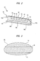
- the light source unit 11 includes a circuit board 12, a plurality of semiconductor light emitting devices 13 (surface emitting light sources) mounted on the circuit board 12, a lower reflector 14 disposed below the semiconductor light emitting devices 13, and an upper reflector 15 disposed above the semiconductor light emitting devices 13.
- semiconductor light emitting devices 13 surface emitting light sources
- the semiconductor light emitting devices 13 are, for example, light emitting diodes (LEDs).
- the semiconductor light emitting devices 13 are arranged side by side in the lateral direction such that each of the light emitting surfaces of the semiconductor light emitting devices 13 faces forward. Turning on and off of the semiconductor light emitting devices 13 can be controlled individually.
- the lower reflector 14 has an upwardly facing reflecting surface 14a on a lower side of the semiconductor light emitting devices 13.
- the upper reflector 15 has a downwardly facing reflecting surface 15a on an upper side of the semiconductor light emitting devices 13.
- the reflecting surface 14a is formed as, for example, a paraboloidal surface.
- the entire surface of the reflecting surface 14a is roughened by sandblasting or the like to provide diffusing portions 14b for diffusing light (see Fig. 2 ). Therefore, the reflecting surface 14a is configured to reflect and to diffuse light.
- the reflecting surface 15a is formed as, for example, a hyperboloidal surface.
- the reflecting surface 14a may be formed with convex portions and/or concave portions, instead of being roughened by sandblasting or the like.
- the high beam light distribution pattern P1 includes a pattern T1 formed by light reflected by the reflecting surface 14a, a pattern M formed by light not reflected by the reflecting surfaces 14a, 15a, and a pattern B formed by light reflected by the reflecting surface 15a.
- the pattern T1 forms the upper portion of the light distribution pattern P1
- the pattern M forms the vertically central portion of the light distribution pattern P1
- the pattern B forms the lower portion of the light distribution pattern P1.
- a lens holder 16 is mounted on the front surface of the bracket 7 (see Fig. 1 ).
- the lens holder 16 has a cylindrical shape extending in a front-rear direction, and is mounted on the bracket 7 to surround the semiconductor light emitting devices 13.
- a projection lens 17 is mounted on the front end portion of the lens holder 16.
- the projection lens 17 includes a forwardly convex semispherical lens portion 17a and a flange portion 17b extending from the outer circumference of the lens portion 17a.
- the lens portion 17a and the flange portion 17b are formed as a one-piece structure.
- the projection lens 17 forwardly projects an image formed on a focal plane, including a rear focal point of the projection lens 17, by the light from the semiconductor light emitting devices 13 in an inverted manner.
- the bracket 7, the heat dissipating fins 9, the fan 10, the light source unit 11, the lens holder 16 and the projection lens 17 together form the lamp unit 6 projecting a high beam for irradiating a long range.
- the optical axis adjusting mechanism 8 includes aiming screws 18.
- the aiming screws 18 extend in the front-rear direction , and are rotatably supported on the rear end portion of the lamp body 2 The aiming screws 18 are respectively threadedly engaged with the bracket 7 at their given positions, thereby connecting the lamp body 2 and bracket 7.
- the lamp unit 6 When one of the aiming screw 18 is rotated, the lamp unit 6 is turned in a direction corresponding to the rotating direction with the other aiming screws serving as a fulcrum, whereby an aiming adjustment of the lamp unit 6 is carried out.
- the vehicle headlamp 1 may also include a so-called leveling adjusting mechanism for adjusting the direction of the optical axis to compensate for the change of the direction of the optical axis due to the weight of load carried on a vehicle.
- a vehicle on which the vehicle headlamp 1 is mounted includes a camera having, for example, a charge coupled device (CCD) as an imaging device.
- the camera periodically captures an image of the high beam irradiation area irradiated by the high beam light distribution pattern P1.
- image data is generated, whereby the existence of a forward vehicle 100 in the high beam irradiation area is detected through an image processing.
- the semiconductor light emitting devices 13 emit light.
- the light emitted by the semiconductor light emitting devices 13 travels forwardly or is reflected by one of the reflecting surfaces 14a, 15a, and is converged on a focal plane including the rear focal point of the projection lens 17, whereby high beam is forwardly irradiated through the projection lens 17 and the cover 3. At the same time, images of the high beam irradiation area are captured by the camera.
- the semiconductor light emitting devices 13 are all kept turned on to form the high beam light distribution pattern P1 (see Fig. 3 ).
- the semiconductor light emitting device 13 forming the pattern of the laterally central portion of the high beam light distribution pattern P1 is turned off.
- each of the semiconductor light emitting devices 13 is individually controllable to be turned on and off.
- the semiconductor light emitting device 13 forming the pattern of the laterally central portion of the high beam light distribution pattern P1 is turned off, as shown in Fig. 4 , a portion of the light reflected and diffused by the reflecting surface 14a forms the laterally central portion (the pattern Ta) of the upper pattern T2. That is, the diffusing portions 14b of the reflecting surface 14 function as auxiliary pattern forming means for forming the auxiliary pattern Ta irradiating at least a part of a region that would otherwise be irradiated by the upper portion of the laterally central portion of the high beam light distribution pattern P1 formed by the semiconductor light emitting device 13 that is turned off.
- a non-irradiated dark portion D is provided (see Fig. 4 ).
- the modified light distribution pattern P2 includes an auxiliary pattern T2 (patterns Ta + Tb + Tc) formed by the light reflected by the reflecting surface 14a, lateral patterns Ma, Mb formed on respective sides of the dark portion D by the light not reflected by the reflecting surfaces 14a, 15a, and lateral patterns Ba, Bb formed on respective sides of the dark portion D by the light reflected by the reflecting surface 15a.
- auxiliary pattern T2 patterns Ta + Tb + Tc
- the diffusing portions 14b are formed as auxiliary pattern forming means on the lower reflector 14 to diffuse light emitted by the semiconductor light emitting devices 13, thereby forming the auxiliary pattern Ta of the upper portion of the laterally central portion of the modified light distribution pattern P2. Accordingly, the auxiliary pattern Ta can be formed by a simple structure.
- the diffusing portions 14b functioning as the auxiliary pattern forming means are formed on the lower reflector 14 for reflecting the lights emitted by the semiconductor light emitting devices 13, it is not necessary to provide separate means for forming the pattern Ta. This provides a further advantage in simplifying the structures of the vehicle headlamp 1 and the light source unit 11.
- the light source unit 11A is different from the light source unit 11 in that a rotatable lower reflector 14A, not including a diffusing portion, is provided as auxiliary pattern forming means.
- the light source unit 11A includes a circuit board 12, a plurality of semiconductor light emitting devices 13, a lower reflector 14A and an upper reflector 15 (see Fig. 5 ).
- a drive portion for rotating the lower reflector 14A is disposed below the semiconductor light emitting devices 13.
- a pivot shaft 19 is rotatably supported below the semiconductor light emitting devices 13, a pivot shaft 19 is rotatably supported.
- the pivot shaft 19 extends in the direction in which the semiconductor light emitting devices 13 are arranged, i.e., in the lateral direction.
- the lower reflector 14A is rotatable about the pivot shaft 19 such that the front end portion of the lower reflector 14A moves up and down.
- the lower reflector 14A is rotatable between a first position H and a second position L below the first position H.
- the lower reflector 14A is a plate-like member, and has an upwardly facing surface and a downwardly facing surface.
- the upwardly facing surface of the lower reflector 14A on a side of the semiconductor light emitting devices 13 is formed as a reflecting surface 14c.
- the reflecting surface 14c is formed as, for example, a paraboloidal surface.
- the reflecting surface 14c forwardly reflects light emitted by the semiconductor light emitting devices 13.
- the light reflected by the reflecting surface 14 form the upper pattern T1 (see Fig. 3 ).
- the lower reflector 14A When the pivot shaft 19 is rotated by the driving portion, the lower reflector 14A is rotated in a range between the first position H and second position L in accordance with the rotation of the pivot shaft 19 (see Fig. 5 ).
- the position of an image formed by the reflecting surface 14c coincides with the focal plane of the projection lens 17, whereby the clear upper pattern T1 is formed.
- the position of an image formed by the reflecting surface 14c is shifted from the focal plane of the projection lens 17, whereby a blurred auxiliary pattern T3 is formed.
- the lower reflector 14A is maintained at the first position H and the semiconductor light emitting devices 13 are all turned on, thereby forming the high beam light distribution pattern P1 (see Fig. 3 ).
- the semiconductor light emitting device 13 forming the laterally central portion of the light distribution pattern P1 is turned off, and the lower reflector 14A is rotated from the first position H to the second position L.
- the semiconductor light emitting device 13 forming the laterally central portion of the light distribution pattern P1 is turned off and the lower reflector 14A is rotated to the second position L, a portion of the light reflected by the reflecting surface 14c irradiates at least a part of a region that would otherwise be irradiated by the upper portion of the laterally central portion of the light distribution pattern T1, whereby a modified light distribution pattern P3 including the blurred auxiliary pattern T3 is formed (see Fig. 6 ). Therefore, the region corresponding to a portion of the laterally central portion of the high beam light distribution pattern P1 other than the upper portion is provided as a dark region D.
- the lower reflector 14A is configured to be rotatable to provide auxiliary pattern forming means.
- the high beam light distribution pattern P1 is formed clear with the semiconductor light emitting devices 13 being all turned on, and when the semiconductor light emitting device 13 forming the laterally central portion of the high beam light distribution pattern P1 is turned off, the upper auxiliary pattern T3 can be formed by a simple structure.
- the light source unit 11B is different from the light source unit 11 in that a lower reflector 14B does not include a diffusing portion, and in that an auxiliary light source 20 is provided in addition to the semiconductor light emitting devices 13 as auxiliary pattern forming means.
- the light source unit 11B includes a circuit board 12, a plurality of semiconductor light emitting devices 13, a lower reflector 14B, an upper reflector 15 and an auxiliary light source 20 (see Fig. 7 ).
- the lower reflector 14B includes a upwardly facing reflecting surface 14c on a side of the semiconductor light emitting devices 13.
- the reflecting surface 14c does not include a diffusing portion.
- the auxiliary light source 20 is mounted on a lower portion of the circuit board 12 to serve as auxiliary pattern forming means.
- the auxiliary light source 20 is, for example, a surface emitting light source such as a semiconductor light emitting device.
- the auxiliary light source 20 is oriented such that the light emitting surface of the auxiliary light source 20 faces forward and obliquely upward toward the projection lens 17. Light emitted by the auxiliary light source 20 forms the laterally central portion of an auxiliary pattern T4.
- the semiconductor light emitting devices 13 are all turned on to form the high beam light distribution pattern P1 (see Fig. 3 ), and the auxiliary light source 20 is turned off.
- the semiconductor light emitting device 13 forming the laterally central portion of the high beam light distribution pattern P1 is turned off, and the auxiliary light source 20 is turned on.
- the semiconductor light emitting devices 13 forming the laterally central portion of the high beam light distribution pattern P1 When the semiconductor light emitting devices 13 forming the laterally central portion of the high beam light distribution pattern P1 is turned off and the auxiliary light source 20 is turned on, the light emitted by the auxiliary light source 20 forms the laterally central portion of the auxiliary pattern T4, whereby a modified light distribution pattern P4 is formed (see Fig. 8 ). Therefore, the region of the laterally central portion of the high beam irradiation area other than the upper region thereof is formed as a dark region D.
- the auxiliary light source 20 which is a light source different from the semiconductor light emitting devices 13, is provided as auxiliary pattern forming means. Therefore, the lower reflector 14B can be designed without considering the formation of the upper portion pattern when the semiconductor light emitting device 13 forming the laterally central portion of the high beam light distribution pattern P1 is turned off. Thus, it is possible to improve design flexibility of the lower reflector 14B.
- the high beam light distribution pattern P1 is formed clear with the semiconductor light emitting devices 13 being all turned on, and when the semiconductor light emitting device 13 forming the laterally central portion of the high beam light distribution pattern P1 is turned off, the upper auxiliary pattern T4 is formed with a simple structure.
- the auxiliary light source 20 is arranged on the lower end portion of the circuit board 12.
- the position of the auxiliary light source 20 is not limited to the lower end portion of the circuit board 12. That is, the auxiliary light source 20 may be disposed at position on the circuit board 12, for example, the upper end portion or the lateral end portion of the circuit board 12.
- the number of semiconductor light emitting devices 13 to be turned off when the forward vehicle 100 is detected in the high beam irradiation area is not limited to one, and may be more than one.
Landscapes
- Engineering & Computer Science (AREA)
- General Engineering & Computer Science (AREA)
- Physics & Mathematics (AREA)
- Microelectronics & Electronic Packaging (AREA)
- Optics & Photonics (AREA)
- Non-Portable Lighting Devices Or Systems Thereof (AREA)
- Led Device Packages (AREA)
- Lighting Device Outwards From Vehicle And Optical Signal (AREA)
Abstract
Description
- The present invention relates to a vehicle headlamp.
- A related art vehicle headlamp is disclosed in
JP 2008-037240 A - The headlamp is configured to implement a so-called adaptive driving beam (ADB) control in which a high beam light distribution pattern is modified in accordance with a position of a forward vehicle detected by processing images captured by a camera or the like, such that one of the high beam light sources that irradiates a region where the detected vehicle exists is turned off. The existence of a forward vehicle is detected in a range corresponding to the central portion of the high beam light distribution pattern. This control can prevent a glare to other vehicles running in front.
- However, when a light source that forming the central portion of the high beam light distribution pattern is turned off in response to a detection of a forward vehicle, the high beam light distribution pattern is divided in the lateral direction, which may give an odd feeling to the driver.
- Accordingly, it is an object of the present invention to provide a vehicle headlamp which can prevent a glare to other vehicles while suppressing an odd feeling given to the driver.
- According to an illustrative aspect of the present invention, a vehicle headlamp includes a light source unit having a plurality of semiconductor light emitting devices arranged side by side in a lateral direction, each of the semiconductor light emitting devices being individually controllable to be turned on and off, and a lower reflector disposed below the semiconductor light emitting devices, and a projection lens configured to project light emitted by the semiconductor light emitting devices. The lower reflector and the projection lens are configured and arranged such that a portion of the light emitted by the semiconductor light emitting devices is reflected by the lower reflector and projected by the projection lens to form a pattern of an upper portion of a high beam high beam light distribution pattern for irradiating a long range. Auxiliary pattern forming means is provided for forming, when at least one of the semiconductor light emitting devices forming a laterally central portion of the high beam light distribution pattern is turned off, a auxiliary pattern irradiating at least a part of a region that would otherwise be irradiated with an upper portion of the central portion of the high beam light distribution pattern formed by said at least one of the semiconductor light emitting devices.
- Other aspects and advantages of the invention will be apparent from the following description, the drawings and the claims.
- Hereinafter, embodiments of the present invention will be described with reference to the drawings.
-
-
Fig. 1 is a schematic longitudinal section view of a vehicle headlamp according to an embodiment of the present invention; -
Fig. 2 is an enlarged perspective view of a light source unit of the vehicle headlamp; -
Fig. 3 is a diagram illustrating a high beam light distribution pattern; -
Fig. 4 is a diagram of a modified light distribution pattern which is formed when a forward vehicle is detected; -
Fig. 5 is a side view of a first modified example of the light source unit; -
Fig. 6 is a diagram illustrating a modified light distribution pattern which is formed when a forward vehicle is detected, using the light source unit shown inFig. 5 ; -
Fig. 7 is a side view of a second modified example of the light source unit; and -
Fig. 8 is a diagram illustrating a modified light distribution pattern which is formed when a forward vehicle is detected, using the light source unit shown inFig. 7 . - Firstly, a
vehicle headlamp 1 according to an embodiment of the present invention will be described with reference toFigs. 1 to 4 . - The
vehicle headlamp 1 is mounted on each lateral side of a front end of a vehicle body. - As shown in
Fig. 1 , thevehicle headlamp 1 includes alamp body 2 having a front opening, acover 3 attached to the front portion of thelamp body 2 to form alamp housing 4 having alamp chamber 5, and alamp unit 6 is disposed inside thelamp chamber 5. - Inside the
lamp chamber 5, abracket 7 is provided such that thebracket 7 can be turned horizontally and vertically via an opticalaxis adjusting mechanism 8. - The
bracket 7 is formed like a flat plate, and has a front surface and a rear surface. On the rear surface of thebracket 7,heat dissipating fins 9 are provided to protrude rearward. The heat dissipating fins 9 spaced from each other in the lateral direction. - A
heat dissipating fan 10 is attached to rear surfaces of the heat dissipating fins 9. - A
light source unit 11 is mounted on the central portion of the front surface of thebracket 7. - As shown in
Figs. 1 and2 , thelight source unit 11 includes acircuit board 12, a plurality of semiconductor light emitting devices 13 (surface emitting light sources) mounted on thecircuit board 12, alower reflector 14 disposed below the semiconductorlight emitting devices 13, and anupper reflector 15 disposed above the semiconductorlight emitting devices 13. - The semiconductor
light emitting devices 13 are, for example, light emitting diodes (LEDs). The semiconductorlight emitting devices 13 are arranged side by side in the lateral direction such that each of the light emitting surfaces of the semiconductorlight emitting devices 13 faces forward. Turning on and off of the semiconductorlight emitting devices 13 can be controlled individually. - The
lower reflector 14 has an upwardly facing reflectingsurface 14a on a lower side of the semiconductorlight emitting devices 13. Theupper reflector 15 has a downwardly facing reflectingsurface 15a on an upper side of the semiconductorlight emitting devices 13. - The reflecting
surface 14a is formed as, for example, a paraboloidal surface. The entire surface of the reflectingsurface 14a is roughened by sandblasting or the like to providediffusing portions 14b for diffusing light (seeFig. 2 ). Therefore, the reflectingsurface 14a is configured to reflect and to diffuse light. The reflectingsurface 15a is formed as, for example, a hyperboloidal surface. - To provide the
diffusing portions 14b, the reflectingsurface 14a may be formed with convex portions and/or concave portions, instead of being roughened by sandblasting or the like. - Each of the reflecting
surfaces light emitting devices 13. When lights are emitted by the semiconductorlight emitting devices 13, as shown inFig. 3 , a high beam light distribution pattern P1 is formed. The high beam light distribution pattern P1 includes a pattern T1 formed by light reflected by the reflectingsurface 14a, a pattern M formed by light not reflected by the reflectingsurfaces reflecting surface 15a. - The pattern T1 forms the upper portion of the light distribution pattern P1, the pattern M forms the vertically central portion of the light distribution pattern P1, and the pattern B forms the lower portion of the light distribution pattern P1.
- A
lens holder 16 is mounted on the front surface of the bracket 7 (seeFig. 1 ). Thelens holder 16 has a cylindrical shape extending in a front-rear direction, and is mounted on thebracket 7 to surround the semiconductorlight emitting devices 13. - A
projection lens 17 is mounted on the front end portion of thelens holder 16. Theprojection lens 17 includes a forwardly convexsemispherical lens portion 17a and aflange portion 17b extending from the outer circumference of thelens portion 17a. Thelens portion 17a and theflange portion 17b are formed as a one-piece structure. Theprojection lens 17 forwardly projects an image formed on a focal plane, including a rear focal point of theprojection lens 17, by the light from the semiconductorlight emitting devices 13 in an inverted manner. - The
bracket 7, the heat dissipating fins 9, thefan 10, thelight source unit 11, thelens holder 16 and theprojection lens 17 together form thelamp unit 6 projecting a high beam for irradiating a long range. - The optical
axis adjusting mechanism 8 includes aimingscrews 18. The aimingscrews 18 extend in the front-rear direction , and are rotatably supported on the rear end portion of thelamp body 2 The aimingscrews 18 are respectively threadedly engaged with thebracket 7 at their given positions, thereby connecting thelamp body 2 andbracket 7. - When one of the aiming
screw 18 is rotated, thelamp unit 6 is turned in a direction corresponding to the rotating direction with the other aiming screws serving as a fulcrum, whereby an aiming adjustment of thelamp unit 6 is carried out. - The
vehicle headlamp 1 may also include a so-called leveling adjusting mechanism for adjusting the direction of the optical axis to compensate for the change of the direction of the optical axis due to the weight of load carried on a vehicle. - A vehicle on which the
vehicle headlamp 1 is mounted includes a camera having, for example, a charge coupled device (CCD) as an imaging device. The camera periodically captures an image of the high beam irradiation area irradiated by the high beam light distribution pattern P1. When an image of the high beam irradiation area is captured by the camera, image data is generated, whereby the existence of aforward vehicle 100 in the high beam irradiation area is detected through an image processing. - In the
vehicle headlamp 1 having the configuration described above, when a drive voltage is applied to thelight source unit 11 via a lighting circuit, the semiconductorlight emitting devices 13 emit light. - The light emitted by the semiconductor
light emitting devices 13 travels forwardly or is reflected by one of the reflectingsurfaces projection lens 17, whereby high beam is forwardly irradiated through theprojection lens 17 and thecover 3. At the same time, images of the high beam irradiation area are captured by the camera. - During the high beam irradiation, while a
forward vehicle 100 is not detected in the high beam irradiation area through the image processing, the semiconductorlight emitting devices 13 are all kept turned on to form the high beam light distribution pattern P1 (seeFig. 3 ). When aforward vehicle 100 is detected in the high beam irradiation area, the semiconductorlight emitting device 13 forming the pattern of the laterally central portion of the high beam light distribution pattern P1 is turned off. - As described above, in the
vehicle headlamp 1, each of the semiconductorlight emitting devices 13 is individually controllable to be turned on and off. When the semiconductorlight emitting device 13 forming the pattern of the laterally central portion of the high beam light distribution pattern P1 is turned off, as shown inFig. 4 , a portion of the light reflected and diffused by the reflectingsurface 14a forms the laterally central portion (the pattern Ta) of the upper pattern T2. That is, the diffusingportions 14b of the reflectingsurface 14 function as auxiliary pattern forming means for forming the auxiliary pattern Ta irradiating at least a part of a region that would otherwise be irradiated by the upper portion of the laterally central portion of the high beam light distribution pattern P1 formed by the semiconductorlight emitting device 13 that is turned off. - As described above, when the semiconductor
light emitting device 13 forming the laterally central portion of the high beam light distribution pattern P1 is turned off, in the region where theforward vehicle 100 exists, i.e., in the region between the lateral patterns Ma, Ba, Mb, Bb, a non-irradiated dark portion D is provided (seeFig. 4 ). - As shown in
Fig. 4 , when aforward vehicle 100 is detected in the high beam irradiation area, a modified light distribution pattern P2 is formed. The modified light distribution pattern P2 includes an auxiliary pattern T2 (patterns Ta + Tb + Tc) formed by the light reflected by the reflectingsurface 14a, lateral patterns Ma, Mb formed on respective sides of the dark portion D by the light not reflected by the reflectingsurfaces surface 15a. - As described above, according to the
light source unit 11, the diffusingportions 14b are formed as auxiliary pattern forming means on thelower reflector 14 to diffuse light emitted by the semiconductorlight emitting devices 13, thereby forming the auxiliary pattern Ta of the upper portion of the laterally central portion of the modified light distribution pattern P2. Accordingly, the auxiliary pattern Ta can be formed by a simple structure. - Also, because the diffusing
portions 14b functioning as the auxiliary pattern forming means are formed on thelower reflector 14 for reflecting the lights emitted by the semiconductorlight emitting devices 13, it is not necessary to provide separate means for forming the pattern Ta. This provides a further advantage in simplifying the structures of thevehicle headlamp 1 and thelight source unit 11. - Next, a
light source unit 11A according to a first modified example will be described with reference toFigs. 5 and 6 . Thelight source unit 11A is different from thelight source unit 11 in that a rotatablelower reflector 14A, not including a diffusing portion, is provided as auxiliary pattern forming means. - Therefore, for the
light source unit 11A, features that are different from thelight source unit 11 will be described in detail, and the features that are similar to thelight source unit 11 will be given the same reference signs and description thereof will be omitted or simplified. - The
light source unit 11A includes acircuit board 12, a plurality of semiconductorlight emitting devices 13, alower reflector 14A and an upper reflector 15 (seeFig. 5 ). - A drive portion for rotating the
lower reflector 14A is disposed below the semiconductorlight emitting devices 13. - Below the semiconductor
light emitting devices 13, apivot shaft 19 is rotatably supported. Thepivot shaft 19 extends in the direction in which the semiconductorlight emitting devices 13 are arranged, i.e., in the lateral direction. Thelower reflector 14A is rotatable about thepivot shaft 19 such that the front end portion of thelower reflector 14A moves up and down. Thelower reflector 14A is rotatable between a first position H and a second position L below the first position H. - The
lower reflector 14A is a plate-like member, and has an upwardly facing surface and a downwardly facing surface. The upwardly facing surface of thelower reflector 14A on a side of the semiconductorlight emitting devices 13 is formed as a reflectingsurface 14c. The reflectingsurface 14c is formed as, for example, a paraboloidal surface. - The reflecting
surface 14c forwardly reflects light emitted by the semiconductorlight emitting devices 13. The light reflected by the reflectingsurface 14 form the upper pattern T1 (seeFig. 3 ). - When the
pivot shaft 19 is rotated by the driving portion, thelower reflector 14A is rotated in a range between the first position H and second position L in accordance with the rotation of the pivot shaft 19 (seeFig. 5 ). When thelower reflector 14A is at the first position H, the position of an image formed by the reflectingsurface 14c coincides with the focal plane of theprojection lens 17, whereby the clear upper pattern T1 is formed. When thelower reflector 14A is at the second position L, the position of an image formed by the reflectingsurface 14c is shifted from the focal plane of theprojection lens 17, whereby a blurred auxiliary pattern T3 is formed. - During the high beam irradiation, while a
forward vehicle 100 is not detected, thelower reflector 14A is maintained at the first position H and the semiconductorlight emitting devices 13 are all turned on, thereby forming the high beam light distribution pattern P1 (seeFig. 3 ). When aforward vehicle 100 is detected, the semiconductorlight emitting device 13 forming the laterally central portion of the light distribution pattern P1 is turned off, and thelower reflector 14A is rotated from the first position H to the second position L. - When the semiconductor
light emitting device 13 forming the laterally central portion of the light distribution pattern P1 is turned off and thelower reflector 14A is rotated to the second position L, a portion of the light reflected by the reflectingsurface 14c irradiates at least a part of a region that would otherwise be irradiated by the upper portion of the laterally central portion of the light distribution pattern T1, whereby a modified light distribution pattern P3 including the blurred auxiliary pattern T3 is formed (seeFig. 6 ). Therefore, the region corresponding to a portion of the laterally central portion of the high beam light distribution pattern P1 other than the upper portion is provided as a dark region D. - In the
light source unit 11A, thelower reflector 14A is configured to be rotatable to provide auxiliary pattern forming means. - Therefore, the high beam light distribution pattern P1 is formed clear with the semiconductor
light emitting devices 13 being all turned on, and when the semiconductorlight emitting device 13 forming the laterally central portion of the high beam light distribution pattern P1 is turned off, the upper auxiliary pattern T3 can be formed by a simple structure. - Next, a
light source unit 11B according to a second modified example will be described with reference toFigs. 7 and 8 . Thelight source unit 11B is different from thelight source unit 11 in that alower reflector 14B does not include a diffusing portion, and in that an auxiliarylight source 20 is provided in addition to the semiconductorlight emitting devices 13 as auxiliary pattern forming means. - Therefore, for the
light source unit 11B, features that are different from thelight source unit 11 will be described in detail, and the features that are similar to thelight source unit 11 will be given the same reference signs and description thereof will be omitted or simplified. - The
light source unit 11B includes acircuit board 12, a plurality of semiconductorlight emitting devices 13, alower reflector 14B, anupper reflector 15 and an auxiliary light source 20 (seeFig. 7 ). - The
lower reflector 14B includes a upwardly facing reflectingsurface 14c on a side of the semiconductorlight emitting devices 13. The reflectingsurface 14c does not include a diffusing portion. - The auxiliary
light source 20 is mounted on a lower portion of thecircuit board 12 to serve as auxiliary pattern forming means. The auxiliarylight source 20 is, for example, a surface emitting light source such as a semiconductor light emitting device. The auxiliarylight source 20 is oriented such that the light emitting surface of the auxiliarylight source 20 faces forward and obliquely upward toward theprojection lens 17. Light emitted by the auxiliarylight source 20 forms the laterally central portion of an auxiliary pattern T4. - During the high beam irradiation, while a
forward vehicle 100 is not detected, the semiconductorlight emitting devices 13 are all turned on to form the high beam light distribution pattern P1 (seeFig. 3 ), and the auxiliarylight source 20 is turned off. When aforward vehicle 100 is detected, the semiconductorlight emitting device 13 forming the laterally central portion of the high beam light distribution pattern P1 is turned off, and the auxiliarylight source 20 is turned on. - When the semiconductor
light emitting devices 13 forming the laterally central portion of the high beam light distribution pattern P1 is turned off and the auxiliarylight source 20 is turned on, the light emitted by the auxiliarylight source 20 forms the laterally central portion of the auxiliary pattern T4, whereby a modified light distribution pattern P4 is formed (seeFig. 8 ). Therefore, the region of the laterally central portion of the high beam irradiation area other than the upper region thereof is formed as a dark region D. - In the
light source unit 11B, the auxiliarylight source 20, which is a light source different from the semiconductorlight emitting devices 13, is provided as auxiliary pattern forming means. Therefore, thelower reflector 14B can be designed without considering the formation of the upper portion pattern when the semiconductorlight emitting device 13 forming the laterally central portion of the high beam light distribution pattern P1 is turned off. Thus, it is possible to improve design flexibility of thelower reflector 14B. - Also, the high beam light distribution pattern P1 is formed clear with the semiconductor
light emitting devices 13 being all turned on, and when the semiconductorlight emitting device 13 forming the laterally central portion of the high beam light distribution pattern P1 is turned off, the upper auxiliary pattern T4 is formed with a simple structure. - In the example described above, the auxiliary
light source 20 is arranged on the lower end portion of thecircuit board 12. However, the position of the auxiliarylight source 20 is not limited to the lower end portion of thecircuit board 12. That is, the auxiliarylight source 20 may be disposed at position on thecircuit board 12, for example, the upper end portion or the lateral end portion of thecircuit board 12. - As described above, according to the
vehicle headlamp 1, when the semiconductorlight emitting device 13 forming the laterally central portion of the high beam light distribution pattern P1 is turned off, a modified light distribution pattern P2, P3, P4, not completely divided in the lateral direction, is formed. - Therefore, a glare to other vehicles can be prevented while suppressing an odd feeling given to the driver.
- In the examples described above, when a
forward vehicle 100 is detected in the high beam irradiation area, one of the semiconductorlight emitting devices 13 forming the laterally central portion of the high beam light distribution pattern P1 is turned off. However, the number of semiconductorlight emitting devices 13 to be turned off when theforward vehicle 100 is detected in the high beam irradiation area is not limited to one, and may be more than one. - While the present invention has been described with reference to certain embodiments thereof, the scope of the present invention is not limited to the embodiments described above, and it will be understood by those skilled in the art that various changes and modifications may be made therein without departing from the scope of the present invention as defined by the appended claims
Claims (15)
- A vehicle headlamp (1) comprising:a light source unit (11, 11A, 11B) including a plurality of semiconductor light emitting devices (13) arranged side by side in a lateral direction, each of the semiconductor light emitting devices (13) being individually controllable to be turned on and off, and a lower reflector (14, 14A, 14B) disposed below the semiconductor light emitting devices (13); anda projection lens (17) configured to project light emitted by the semiconductor light emitting devices (13),wherein the lower reflector (14, 14A, 14B) and the projection lens (17) are configured and arranged such that a portion of the light emitted by the semiconductor light emitting devices (13) is reflected by the lower reflector (14, 14A, 14B) and projected by the projection lens (17) to form a pattern (T1) of an upper portion of a high beam high beam light distribution pattern (P1), andwherein auxiliary pattern forming means is provided for forming, when at least one of the semiconductor light emitting devices (13) forming a laterally central portion of the high beam light distribution pattern (P1) is turned off, a auxiliary pattern (T2, T3, T4) irradiating at least a part of a region that would otherwise be irradiated with an upper portion of the central portion of the high beam light distribution pattern (P1) formed by said at least one of the semiconductor light emitting devices (13).
- The vehicle headlamp (1) according to claim 1, wherein the lower reflector (14) comprises a diffusing portion (14b) to provide the auxiliary pattern forming means, the diffusing portion (14b) being configured to diffuse the portion of the light emitted by the semiconductor light emitting devices (13).
- The vehicle headlamp (1) according to claim 2, wherein the diffusing portion (14b) is a roughened reflecting surface (14a).
- The vehicle headlamp (1) according to claim 1, wherein the lower reflector (14A) is rotatable about a pivot shaft (19) extending in the lateral direction to provide the auxiliary pattern forming means.
- The vehicle headlamp (1) according to claim 4, wherein the lower reflector (14A) is rotatable between a first position (H) and a second position (L) below the first position (H), and when said at least one of the semiconductor light emitting devices (13) is turned off, the lower reflector (14A) is rotated to the second position (L), at which the lower reflector (14A) reflects the portion of the light emitted by the remaining ones of the semiconductor light emitting devices (13) to form a blurred auxiliary pattern (T3).
- The vehicle headlamp (1) according to claim 1, further comprising an auxiliary light source (20) to provide the auxiliary pattern forming means.
- The vehicle headlamp (1) according to claim 6, wherein the auxiliary light source (20) emits light toward the projection lens (17).
- The vehicle headlamp (1) according to any one of the preceding claims, wherein, when said at least one of the semiconductor light emitting devices (13) is turned off, the projection lens (17) projects a modified light distribution pattern (P2, P3, P4) including lateral patterns (Ba, Ma, Bb, Mb) coupled to each other by said auxiliary pattern (T2, T3, T4), wherein a non-irradiated region (D) is provided between the lateral patterns (Ba, Ma, Bb, Mb) and below the auxiliary pattern (T2, T3, T4).
- The vehicle headlamp (1) according to any one of the preceding claims, wherein the light source unit (11, 11A, 11B) further includes a circuit board (12) on which the semiconductor light emitting devices (13) and the lower reflector (14, 14A, 14B) are mounted.
- The vehicle headlamp (1) according to claim 9, wherein the light source unit (11, 11A, 11B) further includes an upper reflector (15) disposed above the semiconductor light emitting devices (13).
- The vehicle headlamp (1) according to claim 10, wherein the upper reflector (15) and the projection lens (17) are configured and arranged such that another portion of the light emitted by the semiconductor light emitting devices (13) is reflected by the upper reflector (15) and projected by the projection lens (17) to form a pattern (B) of a lower portion of the high beam light distribution pattern (P1).
- The vehicle headlamp (1) according to any one of the preceding claims, wherein the semiconductor light emitting devices (13) arranged in a single row.
- The vehicle headlamp (1) according to any one of the preceding claims, wherein the semiconductor light emitting devices (13) are surface light emitting light sources, each having a light emitting surface.
- The vehicle headlamp (1) according to claim 13, wherein the semiconductor light emitting devices (13) are light emitting diodes.
- The vehicle headlamp (1) according to claim 13 or 14, wherein the semiconductor light emitting devices (13) are arranged such that the light emitting surface of each of the semiconductor light emitting devices (13) faces forward toward the projection lens (17).
Applications Claiming Priority (1)
| Application Number | Priority Date | Filing Date | Title |
|---|---|---|---|
| JP2011150698A JP5758724B2 (en) | 2011-07-07 | 2011-07-07 | Vehicle headlamp |
Publications (3)
| Publication Number | Publication Date |
|---|---|
| EP2543927A2 true EP2543927A2 (en) | 2013-01-09 |
| EP2543927A3 EP2543927A3 (en) | 2014-08-06 |
| EP2543927B1 EP2543927B1 (en) | 2018-12-19 |
Family
ID=46466257
Family Applications (1)
| Application Number | Title | Priority Date | Filing Date |
|---|---|---|---|
| EP12175276.0A Not-in-force EP2543927B1 (en) | 2011-07-07 | 2012-07-06 | Vehicle headlamp |
Country Status (3)
| Country | Link |
|---|---|
| EP (1) | EP2543927B1 (en) |
| JP (1) | JP5758724B2 (en) |
| CN (1) | CN102865541B (en) |
Cited By (3)
| Publication number | Priority date | Publication date | Assignee | Title |
|---|---|---|---|---|
| WO2025098930A1 (en) * | 2023-11-08 | 2025-05-15 | Valeo Vision | Lighting module, lighting device and vehicle |
| US20250198587A1 (en) * | 2022-03-07 | 2025-06-19 | Koito Manufacturing Co., Ltd. | Vehicle light |
| EP4459180A4 (en) * | 2021-12-28 | 2025-08-27 | Ichikoh Industries Ltd | LAMP UNIT FOR VEHICLE HEADLIGHTS AND VEHICLE HEADLIGHTS |
Families Citing this family (9)
| Publication number | Priority date | Publication date | Assignee | Title |
|---|---|---|---|---|
| JP5883587B2 (en) * | 2011-07-12 | 2016-03-15 | 株式会社小糸製作所 | Vehicle headlamp |
| JP6724520B2 (en) * | 2016-04-21 | 2020-07-15 | 市光工業株式会社 | Vehicle lighting |
| JP6812695B2 (en) | 2016-08-08 | 2021-01-13 | 市光工業株式会社 | Vehicle lighting |
| JP6790568B2 (en) | 2016-08-09 | 2020-11-25 | 市光工業株式会社 | Vehicle lighting |
| JP6935266B2 (en) * | 2017-08-07 | 2021-09-15 | 株式会社小糸製作所 | Vehicle lighting |
| JP7006430B2 (en) * | 2018-03-23 | 2022-02-10 | 市光工業株式会社 | Vehicle lighting |
| CN111981434B (en) * | 2018-05-31 | 2021-11-30 | 亳州易泽信息科技有限公司 | Transmission method of automobile hood for weakening influence of high beam during meeting |
| CN109177867B (en) * | 2018-10-31 | 2023-03-24 | 华域视觉科技(上海)有限公司 | Intelligent high beam |
| JP7204551B2 (en) * | 2019-03-19 | 2023-01-16 | 株式会社小糸製作所 | Vehicle monitoring system |
Citations (1)
| Publication number | Priority date | Publication date | Assignee | Title |
|---|---|---|---|---|
| JP2008037240A (en) | 2006-08-04 | 2008-02-21 | Toyota Motor Corp | Vehicle headlamp |
Family Cites Families (14)
| Publication number | Priority date | Publication date | Assignee | Title |
|---|---|---|---|---|
| US6861809B2 (en) * | 1998-09-18 | 2005-03-01 | Gentex Corporation | Headlamp control to prevent glare |
| DE19756437A1 (en) * | 1997-12-18 | 1999-06-24 | Bosch Gmbh Robert | Vehicle headlamp with high and dipped beam settings |
| JP4541290B2 (en) * | 2005-12-07 | 2010-09-08 | 株式会社小糸製作所 | Vehicle cornering lamp |
| JP4663548B2 (en) * | 2006-02-24 | 2011-04-06 | 株式会社小糸製作所 | Vehicle headlamp lamp unit |
| JP2008177024A (en) * | 2007-01-18 | 2008-07-31 | Ichikoh Ind Ltd | Vehicle headlamp |
| JP2008243434A (en) * | 2007-03-26 | 2008-10-09 | Koito Mfg Co Ltd | Vehicle headlamp lamp unit |
| US20090052200A1 (en) * | 2007-08-22 | 2009-02-26 | Thomas Tessnow | Single source visible and IR vehicle headlamp |
| EP2193046B1 (en) * | 2007-09-24 | 2011-06-08 | Hella KGaA Hueck & Co. | Projection headlight arrangement for vehicles |
| JP4995748B2 (en) * | 2008-01-29 | 2012-08-08 | 株式会社小糸製作所 | Vehicle headlamp device and control method for vehicle headlamp device |
| JP4895224B2 (en) * | 2008-04-18 | 2012-03-14 | 市光工業株式会社 | Vehicle lighting |
| DE102008036193B4 (en) * | 2008-08-02 | 2020-03-12 | Automotive Lighting Reutlingen Gmbh | Lighting device for a motor vehicle |
| FR2936585B1 (en) * | 2008-09-29 | 2016-05-27 | Valeo Vision Sas | ADAPTIVE LIGHTING DEVICE FOR MOTOR VEHICLE |
| JP5133862B2 (en) * | 2008-12-09 | 2013-01-30 | 株式会社小糸製作所 | Lighting fixtures for vehicles |
| JP5401750B2 (en) * | 2009-11-25 | 2014-01-29 | スタンレー電気株式会社 | Vehicle headlamp |
-
2011
- 2011-07-07 JP JP2011150698A patent/JP5758724B2/en not_active Expired - Fee Related
-
2012
- 2012-07-05 CN CN201210231925.8A patent/CN102865541B/en not_active Expired - Fee Related
- 2012-07-06 EP EP12175276.0A patent/EP2543927B1/en not_active Not-in-force
Patent Citations (1)
| Publication number | Priority date | Publication date | Assignee | Title |
|---|---|---|---|---|
| JP2008037240A (en) | 2006-08-04 | 2008-02-21 | Toyota Motor Corp | Vehicle headlamp |
Cited By (4)
| Publication number | Priority date | Publication date | Assignee | Title |
|---|---|---|---|---|
| EP4459180A4 (en) * | 2021-12-28 | 2025-08-27 | Ichikoh Industries Ltd | LAMP UNIT FOR VEHICLE HEADLIGHTS AND VEHICLE HEADLIGHTS |
| US12410899B2 (en) | 2021-12-28 | 2025-09-09 | Ichikoh Industries, Ltd. | Lamp unit for vehicular headlamp, and vehicular headlamp |
| US20250198587A1 (en) * | 2022-03-07 | 2025-06-19 | Koito Manufacturing Co., Ltd. | Vehicle light |
| WO2025098930A1 (en) * | 2023-11-08 | 2025-05-15 | Valeo Vision | Lighting module, lighting device and vehicle |
Also Published As
| Publication number | Publication date |
|---|---|
| JP5758724B2 (en) | 2015-08-05 |
| EP2543927A3 (en) | 2014-08-06 |
| CN102865541B (en) | 2015-03-18 |
| EP2543927B1 (en) | 2018-12-19 |
| JP2013020709A (en) | 2013-01-31 |
| CN102865541A (en) | 2013-01-09 |
Similar Documents
| Publication | Publication Date | Title |
|---|---|---|
| EP2543927B1 (en) | Vehicle headlamp | |
| US10309606B2 (en) | Vehicle lamp | |
| JP5221174B2 (en) | Vehicle headlamp | |
| US8708539B2 (en) | Vehicular lamp | |
| JP5828424B2 (en) | Vehicle headlamp | |
| JP6941927B2 (en) | Vehicle headlight device | |
| JP5883587B2 (en) | Vehicle headlamp | |
| CN103727475B (en) | Vehicular headlamp | |
| JP6162497B2 (en) | Lamp unit and vehicle lamp | |
| US20250128659A1 (en) | Vehicle light fixture system, light distribution control device, and light distribution control method | |
| JP2012156051A (en) | Vehicle headlamp | |
| WO2016093154A1 (en) | Vehicular illumination device | |
| JP4515391B2 (en) | Vehicle headlamp | |
| CN109237414B (en) | Optical unit | |
| JP5202940B2 (en) | Vehicle headlamp | |
| JP5668158B2 (en) | Vehicle headlamp | |
| JP5486101B2 (en) | Vehicle headlamp | |
| CN111867886B (en) | Vehicle lamps and vehicle lamp systems | |
| WO2023189597A1 (en) | Vehicle lamp | |
| US11415290B2 (en) | Vehicle lamp | |
| JP7101547B2 (en) | Vehicle headlights | |
| JP2010282794A (en) | Vehicle lamp | |
| JP6466691B2 (en) | Vehicle lamp system and control unit | |
| US11674658B2 (en) | Headlamp for vehicle | |
| JP2013033624A (en) | Vehicular headlight |
Legal Events
| Date | Code | Title | Description |
|---|---|---|---|
| PUAI | Public reference made under article 153(3) epc to a published international application that has entered the european phase |
Free format text: ORIGINAL CODE: 0009012 |
|
| 17P | Request for examination filed |
Effective date: 20120706 |
|
| AK | Designated contracting states |
Kind code of ref document: A2 Designated state(s): AL AT BE BG CH CY CZ DE DK EE ES FI FR GB GR HR HU IE IS IT LI LT LU LV MC MK MT NL NO PL PT RO RS SE SI SK SM TR |
|
| AX | Request for extension of the european patent |
Extension state: BA ME |
|
| PUAL | Search report despatched |
Free format text: ORIGINAL CODE: 0009013 |
|
| AK | Designated contracting states |
Kind code of ref document: A3 Designated state(s): AL AT BE BG CH CY CZ DE DK EE ES FI FR GB GR HR HU IE IS IT LI LT LU LV MC MK MT NL NO PL PT RO RS SE SI SK SM TR |
|
| AX | Request for extension of the european patent |
Extension state: BA ME |
|
| RIC1 | Information provided on ipc code assigned before grant |
Ipc: F21W 101/10 20060101ALN20140701BHEP Ipc: B60Q 1/08 20060101ALI20140701BHEP Ipc: F21S 8/10 20060101ALI20140701BHEP Ipc: F21V 7/00 20060101ALI20140701BHEP Ipc: F21Y 101/02 20060101ALN20140701BHEP Ipc: B60Q 1/14 20060101ALI20140701BHEP Ipc: F21V 14/04 20060101ALI20140701BHEP Ipc: F21S 8/12 20060101AFI20140701BHEP |
|
| REG | Reference to a national code |
Ref country code: DE Ref legal event code: R079 Ref document number: 602012054790 Country of ref document: DE Free format text: PREVIOUS MAIN CLASS: F21S0008120000 Ipc: F21V0014040000 |
|
| RIC1 | Information provided on ipc code assigned before grant |
Ipc: F21S 41/143 20180101ALI20180525BHEP Ipc: F21S 41/663 20180101ALI20180525BHEP Ipc: F21V 7/00 20060101ALI20180525BHEP Ipc: F21S 41/37 20180101ALI20180525BHEP Ipc: F21V 14/04 20060101AFI20180525BHEP Ipc: B60Q 1/14 20060101ALI20180525BHEP Ipc: F21S 41/32 20180101ALI20180525BHEP Ipc: B60Q 1/08 20060101ALI20180525BHEP Ipc: F21S 41/675 20180101ALI20180525BHEP |
|
| GRAP | Despatch of communication of intention to grant a patent |
Free format text: ORIGINAL CODE: EPIDOSNIGR1 |
|
| STAA | Information on the status of an ep patent application or granted ep patent |
Free format text: STATUS: GRANT OF PATENT IS INTENDED |
|
| INTG | Intention to grant announced |
Effective date: 20180712 |
|
| GRAS | Grant fee paid |
Free format text: ORIGINAL CODE: EPIDOSNIGR3 |
|
| GRAA | (expected) grant |
Free format text: ORIGINAL CODE: 0009210 |
|
| STAA | Information on the status of an ep patent application or granted ep patent |
Free format text: STATUS: THE PATENT HAS BEEN GRANTED |
|
| AK | Designated contracting states |
Kind code of ref document: B1 Designated state(s): AL AT BE BG CH CY CZ DE DK EE ES FI FR GB GR HR HU IE IS IT LI LT LU LV MC MK MT NL NO PL PT RO RS SE SI SK SM TR |
|
| REG | Reference to a national code |
Ref country code: GB Ref legal event code: FG4D |
|
| REG | Reference to a national code |
Ref country code: CH Ref legal event code: EP |
|
| REG | Reference to a national code |
Ref country code: IE Ref legal event code: FG4D |
|
| REG | Reference to a national code |
Ref country code: DE Ref legal event code: R096 Ref document number: 602012054790 Country of ref document: DE |
|
| REG | Reference to a national code |
Ref country code: AT Ref legal event code: REF Ref document number: 1079133 Country of ref document: AT Kind code of ref document: T Effective date: 20190115 |
|
| REG | Reference to a national code |
Ref country code: NL Ref legal event code: MP Effective date: 20181219 |
|
| PG25 | Lapsed in a contracting state [announced via postgrant information from national office to epo] |
Ref country code: LV Free format text: LAPSE BECAUSE OF FAILURE TO SUBMIT A TRANSLATION OF THE DESCRIPTION OR TO PAY THE FEE WITHIN THE PRESCRIBED TIME-LIMIT Effective date: 20181219 Ref country code: LT Free format text: LAPSE BECAUSE OF FAILURE TO SUBMIT A TRANSLATION OF THE DESCRIPTION OR TO PAY THE FEE WITHIN THE PRESCRIBED TIME-LIMIT Effective date: 20181219 Ref country code: HR Free format text: LAPSE BECAUSE OF FAILURE TO SUBMIT A TRANSLATION OF THE DESCRIPTION OR TO PAY THE FEE WITHIN THE PRESCRIBED TIME-LIMIT Effective date: 20181219 Ref country code: BG Free format text: LAPSE BECAUSE OF FAILURE TO SUBMIT A TRANSLATION OF THE DESCRIPTION OR TO PAY THE FEE WITHIN THE PRESCRIBED TIME-LIMIT Effective date: 20190319 Ref country code: FI Free format text: LAPSE BECAUSE OF FAILURE TO SUBMIT A TRANSLATION OF THE DESCRIPTION OR TO PAY THE FEE WITHIN THE PRESCRIBED TIME-LIMIT Effective date: 20181219 Ref country code: NO Free format text: LAPSE BECAUSE OF FAILURE TO SUBMIT A TRANSLATION OF THE DESCRIPTION OR TO PAY THE FEE WITHIN THE PRESCRIBED TIME-LIMIT Effective date: 20190319 |
|
| REG | Reference to a national code |
Ref country code: LT Ref legal event code: MG4D |
|
| REG | Reference to a national code |
Ref country code: AT Ref legal event code: MK05 Ref document number: 1079133 Country of ref document: AT Kind code of ref document: T Effective date: 20181219 |
|
| PG25 | Lapsed in a contracting state [announced via postgrant information from national office to epo] |
Ref country code: RS Free format text: LAPSE BECAUSE OF FAILURE TO SUBMIT A TRANSLATION OF THE DESCRIPTION OR TO PAY THE FEE WITHIN THE PRESCRIBED TIME-LIMIT Effective date: 20181219 Ref country code: SE Free format text: LAPSE BECAUSE OF FAILURE TO SUBMIT A TRANSLATION OF THE DESCRIPTION OR TO PAY THE FEE WITHIN THE PRESCRIBED TIME-LIMIT Effective date: 20181219 Ref country code: GR Free format text: LAPSE BECAUSE OF FAILURE TO SUBMIT A TRANSLATION OF THE DESCRIPTION OR TO PAY THE FEE WITHIN THE PRESCRIBED TIME-LIMIT Effective date: 20190320 Ref country code: AL Free format text: LAPSE BECAUSE OF FAILURE TO SUBMIT A TRANSLATION OF THE DESCRIPTION OR TO PAY THE FEE WITHIN THE PRESCRIBED TIME-LIMIT Effective date: 20181219 |
|
| PG25 | Lapsed in a contracting state [announced via postgrant information from national office to epo] |
Ref country code: NL Free format text: LAPSE BECAUSE OF FAILURE TO SUBMIT A TRANSLATION OF THE DESCRIPTION OR TO PAY THE FEE WITHIN THE PRESCRIBED TIME-LIMIT Effective date: 20181219 |
|
| PG25 | Lapsed in a contracting state [announced via postgrant information from national office to epo] |
Ref country code: ES Free format text: LAPSE BECAUSE OF FAILURE TO SUBMIT A TRANSLATION OF THE DESCRIPTION OR TO PAY THE FEE WITHIN THE PRESCRIBED TIME-LIMIT Effective date: 20181219 Ref country code: IT Free format text: LAPSE BECAUSE OF FAILURE TO SUBMIT A TRANSLATION OF THE DESCRIPTION OR TO PAY THE FEE WITHIN THE PRESCRIBED TIME-LIMIT Effective date: 20181219 Ref country code: CZ Free format text: LAPSE BECAUSE OF FAILURE TO SUBMIT A TRANSLATION OF THE DESCRIPTION OR TO PAY THE FEE WITHIN THE PRESCRIBED TIME-LIMIT Effective date: 20181219 Ref country code: PT Free format text: LAPSE BECAUSE OF FAILURE TO SUBMIT A TRANSLATION OF THE DESCRIPTION OR TO PAY THE FEE WITHIN THE PRESCRIBED TIME-LIMIT Effective date: 20190419 Ref country code: PL Free format text: LAPSE BECAUSE OF FAILURE TO SUBMIT A TRANSLATION OF THE DESCRIPTION OR TO PAY THE FEE WITHIN THE PRESCRIBED TIME-LIMIT Effective date: 20181219 |
|
| PG25 | Lapsed in a contracting state [announced via postgrant information from national office to epo] |
Ref country code: SK Free format text: LAPSE BECAUSE OF FAILURE TO SUBMIT A TRANSLATION OF THE DESCRIPTION OR TO PAY THE FEE WITHIN THE PRESCRIBED TIME-LIMIT Effective date: 20181219 Ref country code: RO Free format text: LAPSE BECAUSE OF FAILURE TO SUBMIT A TRANSLATION OF THE DESCRIPTION OR TO PAY THE FEE WITHIN THE PRESCRIBED TIME-LIMIT Effective date: 20181219 Ref country code: IS Free format text: LAPSE BECAUSE OF FAILURE TO SUBMIT A TRANSLATION OF THE DESCRIPTION OR TO PAY THE FEE WITHIN THE PRESCRIBED TIME-LIMIT Effective date: 20190419 Ref country code: EE Free format text: LAPSE BECAUSE OF FAILURE TO SUBMIT A TRANSLATION OF THE DESCRIPTION OR TO PAY THE FEE WITHIN THE PRESCRIBED TIME-LIMIT Effective date: 20181219 Ref country code: SM Free format text: LAPSE BECAUSE OF FAILURE TO SUBMIT A TRANSLATION OF THE DESCRIPTION OR TO PAY THE FEE WITHIN THE PRESCRIBED TIME-LIMIT Effective date: 20181219 |
|
| PGFP | Annual fee paid to national office [announced via postgrant information from national office to epo] |
Ref country code: FR Payment date: 20190619 Year of fee payment: 8 |
|
| REG | Reference to a national code |
Ref country code: DE Ref legal event code: R097 Ref document number: 602012054790 Country of ref document: DE |
|
| PLBE | No opposition filed within time limit |
Free format text: ORIGINAL CODE: 0009261 |
|
| STAA | Information on the status of an ep patent application or granted ep patent |
Free format text: STATUS: NO OPPOSITION FILED WITHIN TIME LIMIT |
|
| PG25 | Lapsed in a contracting state [announced via postgrant information from national office to epo] |
Ref country code: AT Free format text: LAPSE BECAUSE OF FAILURE TO SUBMIT A TRANSLATION OF THE DESCRIPTION OR TO PAY THE FEE WITHIN THE PRESCRIBED TIME-LIMIT Effective date: 20181219 Ref country code: DK Free format text: LAPSE BECAUSE OF FAILURE TO SUBMIT A TRANSLATION OF THE DESCRIPTION OR TO PAY THE FEE WITHIN THE PRESCRIBED TIME-LIMIT Effective date: 20181219 |
|
| PGFP | Annual fee paid to national office [announced via postgrant information from national office to epo] |
Ref country code: DE Payment date: 20190625 Year of fee payment: 8 |
|
| 26N | No opposition filed |
Effective date: 20190920 |
|
| PG25 | Lapsed in a contracting state [announced via postgrant information from national office to epo] |
Ref country code: SI Free format text: LAPSE BECAUSE OF FAILURE TO SUBMIT A TRANSLATION OF THE DESCRIPTION OR TO PAY THE FEE WITHIN THE PRESCRIBED TIME-LIMIT Effective date: 20181219 Ref country code: MC Free format text: LAPSE BECAUSE OF FAILURE TO SUBMIT A TRANSLATION OF THE DESCRIPTION OR TO PAY THE FEE WITHIN THE PRESCRIBED TIME-LIMIT Effective date: 20181219 |
|
| REG | Reference to a national code |
Ref country code: CH Ref legal event code: PL |
|
| GBPC | Gb: european patent ceased through non-payment of renewal fee |
Effective date: 20190706 |
|
| PG25 | Lapsed in a contracting state [announced via postgrant information from national office to epo] |
Ref country code: TR Free format text: LAPSE BECAUSE OF FAILURE TO SUBMIT A TRANSLATION OF THE DESCRIPTION OR TO PAY THE FEE WITHIN THE PRESCRIBED TIME-LIMIT Effective date: 20181219 |
|
| REG | Reference to a national code |
Ref country code: BE Ref legal event code: MM Effective date: 20190731 |
|
| PG25 | Lapsed in a contracting state [announced via postgrant information from national office to epo] |
Ref country code: GB Free format text: LAPSE BECAUSE OF NON-PAYMENT OF DUE FEES Effective date: 20190706 |
|
| PG25 | Lapsed in a contracting state [announced via postgrant information from national office to epo] |
Ref country code: BE Free format text: LAPSE BECAUSE OF NON-PAYMENT OF DUE FEES Effective date: 20190731 Ref country code: LU Free format text: LAPSE BECAUSE OF NON-PAYMENT OF DUE FEES Effective date: 20190706 Ref country code: CH Free format text: LAPSE BECAUSE OF NON-PAYMENT OF DUE FEES Effective date: 20190731 Ref country code: LI Free format text: LAPSE BECAUSE OF NON-PAYMENT OF DUE FEES Effective date: 20190731 |
|
| PG25 | Lapsed in a contracting state [announced via postgrant information from national office to epo] |
Ref country code: IE Free format text: LAPSE BECAUSE OF NON-PAYMENT OF DUE FEES Effective date: 20190706 |
|
| REG | Reference to a national code |
Ref country code: DE Ref legal event code: R119 Ref document number: 602012054790 Country of ref document: DE |
|
| PG25 | Lapsed in a contracting state [announced via postgrant information from national office to epo] |
Ref country code: FR Free format text: LAPSE BECAUSE OF NON-PAYMENT OF DUE FEES Effective date: 20200731 |
|
| PG25 | Lapsed in a contracting state [announced via postgrant information from national office to epo] |
Ref country code: CY Free format text: LAPSE BECAUSE OF FAILURE TO SUBMIT A TRANSLATION OF THE DESCRIPTION OR TO PAY THE FEE WITHIN THE PRESCRIBED TIME-LIMIT Effective date: 20181219 Ref country code: DE Free format text: LAPSE BECAUSE OF NON-PAYMENT OF DUE FEES Effective date: 20210202 |
|
| PG25 | Lapsed in a contracting state [announced via postgrant information from national office to epo] |
Ref country code: MT Free format text: LAPSE BECAUSE OF FAILURE TO SUBMIT A TRANSLATION OF THE DESCRIPTION OR TO PAY THE FEE WITHIN THE PRESCRIBED TIME-LIMIT Effective date: 20181219 Ref country code: HU Free format text: LAPSE BECAUSE OF FAILURE TO SUBMIT A TRANSLATION OF THE DESCRIPTION OR TO PAY THE FEE WITHIN THE PRESCRIBED TIME-LIMIT; INVALID AB INITIO Effective date: 20120706 |
|
| PG25 | Lapsed in a contracting state [announced via postgrant information from national office to epo] |
Ref country code: MK Free format text: LAPSE BECAUSE OF FAILURE TO SUBMIT A TRANSLATION OF THE DESCRIPTION OR TO PAY THE FEE WITHIN THE PRESCRIBED TIME-LIMIT Effective date: 20181219 |