EP2538248A1 - Dichroic filters formed using silicon carbide based layers - Google Patents
Dichroic filters formed using silicon carbide based layers Download PDFInfo
- Publication number
- EP2538248A1 EP2538248A1 EP12174471A EP12174471A EP2538248A1 EP 2538248 A1 EP2538248 A1 EP 2538248A1 EP 12174471 A EP12174471 A EP 12174471A EP 12174471 A EP12174471 A EP 12174471A EP 2538248 A1 EP2538248 A1 EP 2538248A1
- Authority
- EP
- European Patent Office
- Prior art keywords
- layer
- layers
- depositing
- pairs
- flexible
- Prior art date
- Legal status (The legal status is an assumption and is not a legal conclusion. Google has not performed a legal analysis and makes no representation as to the accuracy of the status listed.)
- Withdrawn
Links
- HBMJWWWQQXIZIP-UHFFFAOYSA-N silicon carbide Chemical compound [Si+]#[C-] HBMJWWWQQXIZIP-UHFFFAOYSA-N 0.000 title claims description 32
- 229910010271 silicon carbide Inorganic materials 0.000 title claims description 20
- 238000000151 deposition Methods 0.000 claims abstract description 69
- 239000000758 substrate Substances 0.000 claims abstract description 53
- 238000000034 method Methods 0.000 claims abstract description 45
- 230000003287 optical effect Effects 0.000 claims abstract description 45
- QVGXLLKOCUKJST-UHFFFAOYSA-N atomic oxygen Chemical compound [O] QVGXLLKOCUKJST-UHFFFAOYSA-N 0.000 claims abstract description 19
- 239000002243 precursor Substances 0.000 claims abstract description 11
- OKTJSMMVPCPJKN-UHFFFAOYSA-N Carbon Chemical compound [C] OKTJSMMVPCPJKN-UHFFFAOYSA-N 0.000 claims abstract description 7
- XUIMIQQOPSSXEZ-UHFFFAOYSA-N Silicon Chemical compound [Si] XUIMIQQOPSSXEZ-UHFFFAOYSA-N 0.000 claims abstract description 4
- 239000000463 material Substances 0.000 claims description 42
- 229910052760 oxygen Inorganic materials 0.000 claims description 31
- 239000001301 oxygen Substances 0.000 claims description 31
- 238000000576 coating method Methods 0.000 claims description 25
- 230000005540 biological transmission Effects 0.000 claims description 23
- 239000011261 inert gas Substances 0.000 claims description 21
- 229910052799 carbon Inorganic materials 0.000 claims description 20
- 239000007789 gas Substances 0.000 claims description 20
- 230000008569 process Effects 0.000 claims description 20
- 239000011248 coating agent Substances 0.000 claims description 19
- 229910052739 hydrogen Inorganic materials 0.000 claims description 19
- 239000001257 hydrogen Substances 0.000 claims description 19
- 238000000623 plasma-assisted chemical vapour deposition Methods 0.000 claims description 18
- UFHFLCQGNIYNRP-UHFFFAOYSA-N Hydrogen Chemical compound [H][H] UFHFLCQGNIYNRP-UHFFFAOYSA-N 0.000 claims description 17
- XLYOFNOQVPJJNP-UHFFFAOYSA-N water Chemical compound O XLYOFNOQVPJJNP-UHFFFAOYSA-N 0.000 claims description 15
- 229920003023 plastic Polymers 0.000 claims description 14
- 229910021417 amorphous silicon Inorganic materials 0.000 claims description 12
- 238000005229 chemical vapour deposition Methods 0.000 claims description 12
- PQDJYEQOELDLCP-UHFFFAOYSA-N trimethylsilane Chemical compound C[SiH](C)C PQDJYEQOELDLCP-UHFFFAOYSA-N 0.000 claims description 8
- 238000012545 processing Methods 0.000 claims description 7
- 239000004033 plastic Substances 0.000 claims description 4
- -1 hydrogen- Chemical class 0.000 abstract description 2
- 238000005033 Fourier transform infrared spectroscopy Methods 0.000 description 10
- 230000008021 deposition Effects 0.000 description 8
- 230000008901 benefit Effects 0.000 description 6
- 238000010276 construction Methods 0.000 description 5
- 239000006185 dispersion Substances 0.000 description 4
- 239000010408 film Substances 0.000 description 4
- 230000000737 periodic effect Effects 0.000 description 4
- 238000005001 rutherford backscattering spectroscopy Methods 0.000 description 4
- 229910052710 silicon Inorganic materials 0.000 description 4
- 239000010703 silicon Substances 0.000 description 4
- 230000003595 spectral effect Effects 0.000 description 4
- 238000004611 spectroscopical analysis Methods 0.000 description 4
- 238000001228 spectrum Methods 0.000 description 4
- 238000013461 design Methods 0.000 description 3
- 238000005240 physical vapour deposition Methods 0.000 description 3
- 238000001020 plasma etching Methods 0.000 description 3
- 238000000411 transmission spectrum Methods 0.000 description 3
- XKRFYHLGVUSROY-UHFFFAOYSA-N Argon Chemical compound [Ar] XKRFYHLGVUSROY-UHFFFAOYSA-N 0.000 description 2
- 238000001157 Fourier transform infrared spectrum Methods 0.000 description 2
- 229910018540 Si C Inorganic materials 0.000 description 2
- 229910018557 Si O Inorganic materials 0.000 description 2
- 230000003667 anti-reflective effect Effects 0.000 description 2
- 230000000903 blocking effect Effects 0.000 description 2
- 238000006243 chemical reaction Methods 0.000 description 2
- 239000003086 colorant Substances 0.000 description 2
- 239000002131 composite material Substances 0.000 description 2
- 238000011161 development Methods 0.000 description 2
- 230000000694 effects Effects 0.000 description 2
- 239000012634 fragment Substances 0.000 description 2
- 239000001307 helium Substances 0.000 description 2
- 229910052734 helium Inorganic materials 0.000 description 2
- SWQJXJOGLNCZEY-UHFFFAOYSA-N helium atom Chemical compound [He] SWQJXJOGLNCZEY-UHFFFAOYSA-N 0.000 description 2
- 150000002431 hydrogen Chemical class 0.000 description 2
- 150000002500 ions Chemical class 0.000 description 2
- 229910044991 metal oxide Inorganic materials 0.000 description 2
- 150000004706 metal oxides Chemical class 0.000 description 2
- 239000000203 mixture Substances 0.000 description 2
- 238000012986 modification Methods 0.000 description 2
- 230000004048 modification Effects 0.000 description 2
- 230000010355 oscillation Effects 0.000 description 2
- 239000002985 plastic film Substances 0.000 description 2
- 229920006255 plastic film Polymers 0.000 description 2
- 229920000139 polyethylene terephthalate Polymers 0.000 description 2
- 239000005020 polyethylene terephthalate Substances 0.000 description 2
- LIVNPJMFVYWSIS-UHFFFAOYSA-N silicon monoxide Inorganic materials [Si-]#[O+] LIVNPJMFVYWSIS-UHFFFAOYSA-N 0.000 description 2
- HMDDXIMCDZRSNE-UHFFFAOYSA-N [C].[Si] Chemical compound [C].[Si] HMDDXIMCDZRSNE-UHFFFAOYSA-N 0.000 description 1
- 238000002835 absorbance Methods 0.000 description 1
- 239000000654 additive Substances 0.000 description 1
- 230000000996 additive effect Effects 0.000 description 1
- 229910052786 argon Inorganic materials 0.000 description 1
- 230000004888 barrier function Effects 0.000 description 1
- 239000006227 byproduct Substances 0.000 description 1
- 230000015556 catabolic process Effects 0.000 description 1
- 229910052729 chemical element Inorganic materials 0.000 description 1
- 238000006731 degradation reaction Methods 0.000 description 1
- KPUWHANPEXNPJT-UHFFFAOYSA-N disiloxane Chemical class [SiH3]O[SiH3] KPUWHANPEXNPJT-UHFFFAOYSA-N 0.000 description 1
- 230000005284 excitation Effects 0.000 description 1
- 238000001914 filtration Methods 0.000 description 1
- 229920002457 flexible plastic Polymers 0.000 description 1
- 230000004907 flux Effects 0.000 description 1
- 238000013467 fragmentation Methods 0.000 description 1
- 238000006062 fragmentation reaction Methods 0.000 description 1
- 238000004519 manufacturing process Methods 0.000 description 1
- 125000004430 oxygen atom Chemical group O* 0.000 description 1
- 239000011112 polyethylene naphthalate Substances 0.000 description 1
- 229920001296 polysiloxane Polymers 0.000 description 1
- 230000035945 sensitivity Effects 0.000 description 1
- 239000000126 substance Substances 0.000 description 1
- 230000002459 sustained effect Effects 0.000 description 1
- 238000012360 testing method Methods 0.000 description 1
- 239000010409 thin film Substances 0.000 description 1
- 238000012546 transfer Methods 0.000 description 1
- 239000012780 transparent material Substances 0.000 description 1
Images



Classifications
-
- G—PHYSICS
- G02—OPTICS
- G02B—OPTICAL ELEMENTS, SYSTEMS OR APPARATUS
- G02B5/00—Optical elements other than lenses
- G02B5/20—Filters
- G02B5/28—Interference filters
- G02B5/285—Interference filters comprising deposited thin solid films
-
- G—PHYSICS
- G02—OPTICS
- G02B—OPTICAL ELEMENTS, SYSTEMS OR APPARATUS
- G02B5/00—Optical elements other than lenses
- G02B5/20—Filters
- G02B5/28—Interference filters
-
- G—PHYSICS
- G02—OPTICS
- G02B—OPTICAL ELEMENTS, SYSTEMS OR APPARATUS
- G02B1/00—Optical elements characterised by the material of which they are made; Optical coatings for optical elements
- G02B1/10—Optical coatings produced by application to, or surface treatment of, optical elements
- G02B1/11—Anti-reflection coatings
Definitions
- This invention relates generally to dichroic filters, and, more particularly, to flexible dichroic filters formed of multiple layers comprising silicon and carbon chemical elements.
- dichroic is derived from the Greek word dikhroos, which means two-colored.
- dichroic refers to any optical device which can split a beam of light into two beams with differing wavelengths.
- Dichroic color filters selectively transmit light with a small range of colors (i.e., a frequency or wavelength range) while reflecting other colors of light.
- Dichroic color filters may be formed by layering multiple thin films or coatings over a surface of a transparent material. The layers or coatings are formed used materials having different refractive indices and are applied in thicknesses of one-quarter or one-half a selected wavelength.
- the wavelength or frequency bands that are transmitted and/or reflected can be controlled by varying the thicknesses and/or the refractive indices of the layers.
- conventional dichroic optical filters are based on a quarter wave stack design, in which alternating layers of high and low refractive index materials are deposited on a transparent substrate in quarter wave optical thicknesses.
- a filter can be designed to transmit specific wavelengths and reflect those which are undesirable.
- Conventional dichroic optical filters are formed of a relatively large number of layers. For example, more than 20 layers of alternating high and low refractive index material may be used to form a conventional dichroic optical filter. Consequently, the deposition time required to form the layers of a conventional dichroic optical filter may be relatively large and the resulting structure may have relatively low mechanical stability. Thus, conventional dichroic filters formed of a large number of layers may be stress inherent and relatively expensive to build. Furthermore, conventional dichroic optical filters are formed using multiple layers of metal oxides that are produced by physical vapor deposition.
- the present invention is directed to addressing the effects of one or more of the problems set forth above.
- the following presents a simplified summary of the invention in order to provide a basic understanding of some aspects of the invention. This summary is not an exhaustive overview of the invention. It is not intended to identify key or critical elements of the invention or to delineate the scope of the invention. Its sole purpose is to present some concepts in a simplified form as a prelude to the more detailed description that is discussed later.
- a method for forming a flexible dichroic optical filter.
- the method comprises depositing a plurality of pairs of layers adjacent a plastic substrate.
- Each of the plurality of pairs of layers includes a first layer formed of a silicon-and-carbon containing material having a first index of refraction and a second layer formed of a silicon-and-carbon containing material having a second index of refraction that is different than the first index of refraction.
- a dichroic optical filter formed by embodiments of this method are also set forth in another embodiment of the present invention.
- FIG. 1 conceptually illustrates one exemplary embodiment of a dichroic filter 100.
- the dichroic filter 100 includes a substrate 105.
- the substrate 105 may be formed of a polyethylene naphthalate (PEN) plastic film, a polyethylene terephthalate (PET) plastic film, and the like.
- PEN polyethylene naphthalate
- PET polyethylene terephthalate
- two dimensions e.g ., a length and a width
- a third dimension e.g ., a thickness
- the substrate 105 may have a diameter of 200 mm and a thickness of 0.13 mm.
- the substrate 105 may be transparent and/or flexible. The degree of transparency and/or flexibility is a matter of design choice and may be selected based upon properties that may be useful and/or desirable for particular implementations of the dichroic filter 100.
- the substrate 105 is exposed to volatile precursors, which may react with and/or decompose on the surface of the substrate 105 to produce the desired deposit and form the layer 110, 115. Volatile byproducts are also produced, which are removed by gas flow through the reaction chamber.
- Plasma enhanced CVD processes utilize plasma to enhance chemical reaction rates of the precursors. PECVD processing may allow deposition at lower temperatures.
- the alternating layers 110, 115 are formed by plasma enhanced chemical vapor deposition using precursor gases that include silicon and carbon.
- a SiC-based dichroic filter 100 may be manufactured by PECVD using trimethylsilane (Z3MS) as a precursor gas to deposit the alternating layers 110, 115 on a flexible transparent polyethylennaphtalate (PEN) substrate 100 using parallel plate (capacitive) reactor, as will be discussed in more detail below.
- the SiC-based dichroic color filter 100 comprises a periodic stack of SiC-based alternating low (L) refractive index (n ⁇ 1.5) material 110 and high (H) refractive index (n ⁇ 1.9) material 115.
- the periodic stack of alternating layers 110, 115 incorporates N of the L/H pairs of layers 110, 115, where N is typically greater than or equal to 10.
- the physical thickness of each layer is given by d H,L .
- the low refractive index layer 110 may be a dielectric high-oxygen doped hydrogenated amorphous silicon carbide coating based on the structural unit SiOC:H.
- the structural unit that is the basis for the material may be evaluated by Energy Dispersion Spectroscopy (EDS) and/or Rutherford Backscattering Spectroscopy (RBS), and the atomic bonding structure may be determined by Fourier Transform InfraRed Spectroscopy (FTIR).
- EDS Energy Dispersion Spectroscopy
- RBS Rutherford Backscattering Spectroscopy
- FTIR Fourier Transform InfraRed Spectroscopy
- the low refractive index layer 110 is deposited at a relatively low plasma power (typically less than 200 W), a relatively low (compared to the high refractive index layer 115) inert gas flow rate (typically less than 800 sccm), and a relatively high (compared to the high refractive index layer 115) oxygen flow rate (typically more than 20 sccm).
- the low refractive index layer 110 may also have a relatively high hydrogen content, low (almost zero) compressive stress, and high transparency (90 % and above).
- the low refractive index layer 110 provides improved transparency and enhanced light transmission, i.e. the low refractive index material 110 may exhibit antireflective properties.
- the high refractive index layer 115 may be a dielectric low-oxygen doped hydrogenated amorphous silicon carbide coating based on the structural unit SiOC:H.
- the structural unit that is the basis for the material may be evaluated by Energy Dispersion Spectroscopy (EDS) and/or Rutherford Backscattering Spectroscopy (RBS), and the atomic bonding structure may be determined by Fourier Transform InfraRed Spectroscopy (FTIR).
- EDS Energy Dispersion Spectroscopy
- RBS Rutherford Backscattering Spectroscopy
- FTIR Fourier Transform InfraRed Spectroscopy
- the high refractive index layer 115 may be deposited at a relatively high plasma power (typically more than 400 W), a relatively high (compared to the low refractive index layer 110) inert gas flow rate (typically more than 800 sccm), and a relatively low (compared to the low refractive index layer 110) oxygen flow rate (typically less than 20 sccm).
- the high refractive index layer 115 may have a relatively low hydrogen content, higher compressive stress (below 400 MPa), and lower transparency (80% and below).
- the spectral characteristics of the dichroic filter 100 may also be determined as a function of the incident light angle.
- the UV VIS transmission and reflection spectra may be determined for incidence angles ranging from 0 to 45 degree.
- Spectral characteristics such as the center wavelength of the reflected band, the reflected bandwidth, the peak transmission, and out-of-band blocking of the dichroic filter 100 have been determined to be a function of both the number of L and H layers 110, 115 and the angle of incident light, as will be discussed further herein.
- the SiC-based dichroic color filter 100 is formed of a periodic stack of SiC-based alternating relatively low refractive index (n ⁇ 1.4) material (L) layers 110 and relatively high refractive index (n ⁇ 1.9) material (H) layers 115.
- the periodic stack includes 10 LH pairs 110, 115.
- Table 1 lists the deposition parameters (process conditions) and the resulting film properties for the low and high refractive index material layers 110, 115.
- the low refractive index material layer 110 has been deposited at low plasma power (150 W), low inert gas flow rate (600 sccm), and a high oxygen flow rate (30 sccm).
- the low refractive index material layer 110 has low (-9 MPa) compressive stress.
- the high refractive index material layer 115 has been deposited at high plasma power (500 W); high inert gas flow rate (1200 sccm) and low oxygen flow rate (15 sccm).
- the high refractive index (RI) material layer 115 has higher compressive stress (-395 MPa). Both, L and H layers are well adhered to the substrate and withstand the standard tape test.
- Figure 2 shows the Fourier transform infrared (FTIR) spectra of low (L) and high (H) refractive index SiOC:H dichroic coatings.
- the absorbance is plotted along the vertical axis in arbitrary units and the wave number is plotted along the horizontal axis in units of cm -1 .
- the FTIR spectrum of the low refractive index coating is plotted using a black line and the FTIR spectrum of the high refractive index coating is plotted using a gray line.
- the low and high refractive index coatings exhibit different features due to different composition and atomic bonding structure of the materials.
- the atomic bonding structure of the high refractive index material layer 115 determined by FTIR, indicates intensive Si-C, Si-O and Si-H stretching oscillations.
- a structural model fragment is illustrated in the inset in Figure 2 that is labeled "H Layer.”
- the atomic bonding structure of the low refractive index material layer 110 determined by FTIR indicates intensive Si-O stretching oscillation as well as minimized Si-C and Si-H one. Due to the high chemical affinity of oxygen toward Si-H radicals, part of the terminating Si-H bonds in the film network have been replaced by bridging oxygen atoms.
- Another structural model fragment is illustrated in the inset in Figure 2 that is labeled "L Layer.”
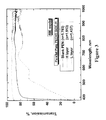
- Figure 3 shows the UV-VIS transmission spectra of a blank polyethylennaphtalate (PEN) substrate, a PEN substrate that is coated with the low refractive index material, and a PEN substrate that is coated with the high refractive index material.
- the transmission percentage is plotted on the vertical axis and wavelength is plotted on the horizontal axis in units of nanometers.
- the substrate that is coated with the low refractive index material has a relatively high transparency (i.e., a transparency of 90 % and above).
- the L coating provides improved transparency and enhanced light transmission relative to the blank substrate, i . e . the low refractive index material exhibits antireflective properties.
- Figures 4A and 4B illustrate spectral characteristics of a multilayer SiC-based dichroic color filter for different light incident angles.
- Figure 4A illustrates a UV-VIS transmission percentage as a function of wavelength in nanometers for several angles of incident light from 0 to 45 degrees
- Figure 4B illustrates a UV-VIS reflection percentage as a function of wavelength in nanometers for several angles of incident light from 0 to 45 degrees.
- the multilayer SiC-based dichroic color filter includes 20 pairs of alternating layers of low and high refractive index material. For twenty layers construction with an optical thickness of the H material of approximately 190 nm (physical thickness of 100 nm), the center wavelength of the reflected band is around 725 nm, which correlates well with the quarter wavelength rule.
- the reflected bandwidth is approximately 150 nm.
- This exemplary dichroic filter can therefore be classified as a notch filter or, more precisely, a red-reflecting dichroic mirror that fully reflects red and transmits yellow, green, cyan, and blue bands. Violet bands are only partially transmitted. Peak transmission is between 65 and 95%, and out-of-band blocking is better than an optical density of 1.5 (transmission less than 3%).
- This exemplary dichroic filter also exhibits sensitivity to the light incidence angles, shifting to shorter wavelengths when the angle of incident light is increased ( Figures 4A and B ).
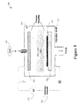
- FIG 5 conceptually illustrates one exemplary embodiment of capacitive type parallel plate reactor 500 that may be used to deposit the alternating layers in a dichroic filter described herein.
- the reactor 500 receives a single wafer 510 and has a showerhead diameter and a hole configuration that provides approximately uniform deposition on 200 mm (8") substrates.
- the plasma is excited and sustained by a 13.56 MHz power supply 515 coupled to the smaller area bottom electrode 520 (which may also act as a substrate holder)
- the top electrode 525 (which also acts as the showerhead) and chamber walls 530 are grounded.
- RIE reactive ion etching
- the large voltage drop results in larger peak ion energies, hence directionality of an accelerated energetic ion flux, which favors precursor excitation and fragmentation, leading to high deposition rates.
- an impedance matching network 535 is interposed between the output of the power supply 515 and the load is driving (plasma) to reduce signal reflections and degradation caused by impedance mismatch.
- the purpose of the impedance matching network 535 is to provide efficient power transfer to the plasma 540 (via power dissipation in the discharge) and to protect the power supply 515.
- a gas source 545 is used to provide one or more gases to the process chamber 505. Although a single gas source 545 is depicted in Figure 5 , persons of ordinary skill in the art having benefit of the present disclosure should appreciate that the present invention is not limited to a single gas source 545. In alternative embodiments, any number of gases 545 may be introduced into the process chamber 505.
- a gas source 545 provides gases including a silicone and carbon to the process chamber.
- the gas source 545 may also provide oxygen, as well as one or more inert gases, such as argon and helium.
- the gas source 545 may provide a gas mixture consisting of trimethylsilane [(CH3)3SiH] as a silicon-carbon containing precursor, with or without helium as an inert gas.
- one side of the substrate 525 is exposed to the plasma in the process chamber 505.
- One or more layers may then be deposited on the substrate 525 while it is exposed to the plasma.
- the plasma is formed from a gas including silicon, carbon, and hydrogen
- a layer may be formed of hydrogenated silicon carbide based on the structural unit SiC:H.
- the plasma is formed from a gas including silicon, carbon, hydrogen, and oxygen
- a layer may be formed of hydrogenated silicon oxycarbide based on the structural unit SiOC:H.
- Operating parameters of the reactor system 500 may be adjusted to achieve certain properties of the layer, such as a selected refractive index, optical thickness, and/or physical thickness. In one embodiment, the operating parameters may be adjusted so that the layer has a relatively high density and low nanoporosity compared to conventional hydrogenated silicon carbide and/or siloxane films.
- the deposition rate of the barrier layer may also depend on one or more of the operating parameters of the reactor system 500. For example, the deposition rates may depend upon the plasma power and chamber pressure.
- the alternating layers that make up embodiments of the dichroic filters described herein may be formed using a single reactor system 500 that uses different operating parameters to form the layers having different refractive indices.
- more than one reactor system 500, or a cluster multi-chamber reactor system that includes a plurality of chambers similar to the chamber shown in Figure 5 may be used to form the layers having different refractive indices.
- Dichroic filters such as the SiC-based optical structures described herein exhibit the dichroic filtering effect with relatively small number of LH pairs (around 20 layers) relative to conventional dichroic filters. Reducing the number of layer pairs is generally advantageous because it may permit deposition times to be reduced and may improve mechanical stability of the structure. This allows flexible dichroic constructions to be realized on transparent plastic substrates.
- conventional dichroic filters that include a large number of layers (N>> 20) are more stress inherent and expensive to build than the dichroic filters described herein. For example, applying the additive rule, the residual stress in a composite SiC-based stack comprising about 20 LH pairs has been estimated to less than 200 MPa.
- the relatively low compressive stress and the good adhesion and thermal stability of the SiC-based dichroic structures make them very convenient to build on flexible plastic substrates.
- the SiC-based dichroic filters may be formed using chemical vapor deposition and/or plasma-enhanced chemical vapor deposition techniques, and therefore may not suffer from the drawbacks of conventional metal oxides-based constructions produced by physical vapor deposition (PVD) methods.
- PVD physical vapor deposition
- subject-matter of the present invention includes subject-matter as defined in the following numbered paragraphs (hereafter "para.”):
Landscapes
- Physics & Mathematics (AREA)
- General Physics & Mathematics (AREA)
- Optics & Photonics (AREA)
- Chemical Vapour Deposition (AREA)
- Laminated Bodies (AREA)
Abstract
Description
- This invention relates generally to dichroic filters, and, more particularly, to flexible dichroic filters formed of multiple layers comprising silicon and carbon chemical elements.
- The term dichroic is derived from the Greek word dikhroos, which means two-colored. When used in the optical arts, the term dichroic refers to any optical device which can split a beam of light into two beams with differing wavelengths. Dichroic color filters selectively transmit light with a small range of colors (i.e., a frequency or wavelength range) while reflecting other colors of light. Dichroic color filters may be formed by layering multiple thin films or coatings over a surface of a transparent material. The layers or coatings are formed used materials having different refractive indices and are applied in thicknesses of one-quarter or one-half a selected wavelength. The wavelength or frequency bands that are transmitted and/or reflected can be controlled by varying the thicknesses and/or the refractive indices of the layers. For example, conventional dichroic optical filters are based on a quarter wave stack design, in which alternating layers of high and low refractive index materials are deposited on a transparent substrate in quarter wave optical thicknesses. Thus, a filter can be designed to transmit specific wavelengths and reflect those which are undesirable.
- Conventional dichroic optical filters are formed of a relatively large number of layers. For example, more than 20 layers of alternating high and low refractive index material may be used to form a conventional dichroic optical filter. Consequently, the deposition time required to form the layers of a conventional dichroic optical filter may be relatively large and the resulting structure may have relatively low mechanical stability. Thus, conventional dichroic filters formed of a large number of layers may be stress inherent and relatively expensive to build. Furthermore, conventional dichroic optical filters are formed using multiple layers of metal oxides that are produced by physical vapor deposition.
- The present invention is directed to addressing the effects of one or more of the problems set forth above. The following presents a simplified summary of the invention in order to provide a basic understanding of some aspects of the invention. This summary is not an exhaustive overview of the invention. It is not intended to identify key or critical elements of the invention or to delineate the scope of the invention. Its sole purpose is to present some concepts in a simplified form as a prelude to the more detailed description that is discussed later.
- In one embodiment of the present invention, a method is provided for forming a flexible dichroic optical filter. The method comprises depositing a plurality of pairs of layers adjacent a plastic substrate. Each of the plurality of pairs of layers includes a first layer formed of a silicon-and-carbon containing material having a first index of refraction and a second layer formed of a silicon-and-carbon containing material having a second index of refraction that is different than the first index of refraction. A dichroic optical filter formed by embodiments of this method are also set forth in another embodiment of the present invention.
- The invention may be understood by reference to the following description taken in conjunction with the accompanying drawings, in which like reference numerals identify like elements, and in which:
-
Figure 1 shows a schematic of a composite multilayer construction of a dichroic color filter with alternating low (L) and high (H) refractive index layers prepared by plasma enhanced chemical vapor deposition (PECVD); -
Figure 2 presents Fourier transform infrared (FTIR) spectra of low (L) and (H) refractive index SiOC:H dichroic coatings, and idealized structural models of coatings are shown in the frames; -
Figure 3 depicts ultraviolet-visible (UV-VIS) transmission spectra of blank, L-coated and H-coated polyethylennaphtalate (PEN) film; -
Figures 4a and 4b present spectral characteristics of multilayer SiC-based dichroic filter for different light incident angles: a) UV-VIS transmission spectra; b) UV-VIS reflection spectra; and -
Figure 5 depicts a schematic of a parallel-plate PECVD reactor in RIE configuration used for manufacturing of dichroic color filters. - While the invention is susceptible to various modifications and alternative forms, specific embodiments thereof have been shown by way of example in the drawings and are herein described in detail. It should be understood, however, that the description herein of specific embodiments is not intended to limit the invention to the particular forms disclosed, but on the contrary, the intention is to cover all modifications, equivalents, and alternatives falling within the scope of the invention as defined by the appended claims.
- Illustrative embodiments of the invention are described below. In the interest of clarity, not all features of an actual implementation are described in this specification. It will of course be appreciated that in the development of any such actual embodiment, numerous implementation-specific decisions should be made to achieve the developers' specific goals, such as compliance with system-related and business-related constraints, which will vary from one implementation to another. Moreover, it will be appreciated that such a development effort might be complex and time-consuming, but would nevertheless be a routine undertaking for those of ordinary skill in the art having the benefit of this disclosure.
- The present invention will now be described with reference to the attached figures. Various structures, systems and devices are schematically depicted in the drawings for purposes of explanation only and so as to not obscure the present invention with details that are well known to those skilled in the art. Nevertheless, the attached drawings are included to describe and explain illustrative examples of the present invention. The words and phrases used herein should be understood and interpreted to have a meaning consistent with the understanding of those words and phrases by those skilled in the relevant art. No special definition of a term or phrase, i.e., a definition that is different from the ordinary and customary meaning as understood by those skilled in the art, is intended to be implied by consistent usage of the term or phrase herein. To the extent that a term or phrase is intended to have a special meaning, i.e., a meaning other than that understood by skilled artisans, such a special definition will be expressly set forth in the specification in a definitional manner that directly and unequivocally provides the special definition for the term or phrase.
-
Figure 1 conceptually illustrates one exemplary embodiment of adichroic filter 100. In the illustrated embodiment, thedichroic filter 100 includes asubstrate 105. For example, thesubstrate 105 may be formed of a polyethylene naphthalate (PEN) plastic film, a polyethylene terephthalate (PET) plastic film, and the like. Persons of ordinary skill in the art having benefit of the present disclosure should appreciate that only a portion of thesubstrate 105 is shown inFigure 1 and that in some embodiments thesubstrate 105 may be sheet of material having two dimensions (e.g., a length and a width) that are significantly larger than a third dimension (e.g., a thickness) of thesubstrate 105. For example, thesubstrate 105 may have a diameter of 200 mm and a thickness of 0.13 mm. In alternative embodiments, thesubstrate 105 may be transparent and/or flexible. The degree of transparency and/or flexibility is a matter of design choice and may be selected based upon properties that may be useful and/or desirable for particular implementations of thedichroic filter 100. -
Alternating layers substrate 105 to build thedichroic filter 100. Although three pairs ofalternating layers Figure 1 , persons of ordinary skill in the art having benefit of the present disclosure should appreciate that the present invention is not limited to this number ofalternating layers alternating layers substrate 105. For example, 20 pairs ofalternating layers substrate 105. Chemical vapor deposition (CVD) and/or plasma-enhanced chemical vapor deposition (PECVD) may be used to deposit thealternating layers substrate 105 is exposed to volatile precursors, which may react with and/or decompose on the surface of thesubstrate 105 to produce the desired deposit and form thelayer - In the illustrated embodiment, the
alternating layers dichroic filter 100 may be manufactured by PECVD using trimethylsilane (Z3MS) as a precursor gas to deposit the alternatinglayers substrate 100 using parallel plate (capacitive) reactor, as will be discussed in more detail below. The SiC-baseddichroic color filter 100 comprises a periodic stack of SiC-based alternating low (L) refractive index (n≤1.5)material 110 and high (H) refractive index (n≥1.9)material 115. The periodic stack of alternatinglayers layers refractive index materials - The low
refractive index layer 110 may be a dielectric high-oxygen doped hydrogenated amorphous silicon carbide coating based on the structural unit SiOC:H. The structural unit that is the basis for the material may be evaluated by Energy Dispersion Spectroscopy (EDS) and/or Rutherford Backscattering Spectroscopy (RBS), and the atomic bonding structure may be determined by Fourier Transform InfraRed Spectroscopy (FTIR). In one embodiment, the lowrefractive index layer 110 is deposited at a relatively low plasma power (typically less than 200 W), a relatively low (compared to the high refractive index layer 115) inert gas flow rate (typically less than 800 sccm), and a relatively high (compared to the high refractive index layer 115) oxygen flow rate (typically more than 20 sccm). The lowrefractive index layer 110 may also have a relatively high hydrogen content, low (almost zero) compressive stress, and high transparency (90 % and above). When deposited on atransparent PEN substrate 105, the lowrefractive index layer 110 provides improved transparency and enhanced light transmission, i.e. the lowrefractive index material 110 may exhibit antireflective properties. - The high
refractive index layer 115 may be a dielectric low-oxygen doped hydrogenated amorphous silicon carbide coating based on the structural unit SiOC:H. The structural unit that is the basis for the material may be evaluated by Energy Dispersion Spectroscopy (EDS) and/or Rutherford Backscattering Spectroscopy (RBS), and the atomic bonding structure may be determined by Fourier Transform InfraRed Spectroscopy (FTIR). The highrefractive index layer 115 may be deposited at a relatively high plasma power (typically more than 400 W), a relatively high (compared to the low refractive index layer 110) inert gas flow rate (typically more than 800 sccm), and a relatively low (compared to the low refractive index layer 110) oxygen flow rate (typically less than 20 sccm). Compared to the lowrefractive index layer 110, the highrefractive index layer 115 may have a relatively low hydrogen content, higher compressive stress (below 400 MPa), and lower transparency (80% and below). - The spectral characteristics of the
dichroic filter 100 may also be determined as a function of the incident light angle. For example, the UV VIS transmission and reflection spectra may be determined for incidence angles ranging from 0 to 45 degree. Spectral characteristics such as the center wavelength of the reflected band, the reflected bandwidth, the peak transmission, and out-of-band blocking of thedichroic filter 100 have been determined to be a function of both the number of L and H layers 110, 115 and the angle of incident light, as will be discussed further herein. - In one exemplary embodiment, the SiC-based
dichroic color filter 100 is formed of a periodic stack of SiC-based alternating relatively low refractive index (n≈1.4) material (L) layers 110 and relatively high refractive index (n≈1.9) material (H) layers 115. The periodic stack includes 10 LHpairs 
In this exemplary embodiment, the low refractive index material is a dielectric high-oxygen doped SiC:H coating with compositional ratios of Si/C=0.58, and O/Si=0.64 as evaluated by Energy Dispersion Spectroscopy (EDS). The high refractive index material is a dielectric low-oxygen doped SiC:H coating with compositional ratios of Si/C=0.80, and O/Si=0.22 as evaluated by Energy Dispersion Spectroscopy (EDS). - Table 1 lists the deposition parameters (process conditions) and the resulting film properties for the low and high refractive index material layers 110, 115. In this exemplary embodiment, the low refractive
index material layer 110 has been deposited at low plasma power (150 W), low inert gas flow rate (600 sccm), and a high oxygen flow rate (30 sccm). The low refractiveindex material layer 110 has low (-9 MPa) compressive stress. The high refractiveindex material layer 115 has been deposited at high plasma power (500 W); high inert gas flow rate (1200 sccm) and low oxygen flow rate (15 sccm). The high refractive index (RI)material layer 115 has higher compressive stress (-395 MPa). Both, L and H layers are well adhered to the substrate and withstand the standard tape test.
-
Figure 2 shows the Fourier transform infrared (FTIR) spectra of low (L) and high (H) refractive index SiOC:H dichroic coatings. The absorbance is plotted along the vertical axis in arbitrary units and the wave number is plotted along the horizontal axis in units of cm-1. The FTIR spectrum of the low refractive index coating is plotted using a black line and the FTIR spectrum of the high refractive index coating is plotted using a gray line. The low and high refractive index coatings exhibit different features due to different composition and atomic bonding structure of the materials. The atomic bonding structure of the high refractiveindex material layer 115 determined by FTIR, indicates intensive Si-C, Si-O and Si-H stretching oscillations. A structural model fragment is illustrated in the inset inFigure 2 that is labeled "H Layer." The atomic bonding structure of the low refractiveindex material layer 110 determined by FTIR indicates intensive Si-O stretching oscillation as well as minimized Si-C and Si-H one. Due to the high chemical affinity of oxygen toward Si-H radicals, part of the terminating Si-H bonds in the film network have been replaced by bridging oxygen atoms. Another structural model fragment is illustrated in the inset inFigure 2 that is labeled "L Layer." -
Figure 3 shows the UV-VIS transmission spectra of a blank polyethylennaphtalate (PEN) substrate, a PEN substrate that is coated with the low refractive index material, and a PEN substrate that is coated with the high refractive index material. The transmission percentage is plotted on the vertical axis and wavelength is plotted on the horizontal axis in units of nanometers. The substrate that is coated with the low refractive index material has a relatively high transparency (i.e., a transparency of 90 % and above). Thus, when deposited on the PEN substrate, the L coating provides improved transparency and enhanced light transmission relative to the blank substrate, i.e. the low refractive index material exhibits antireflective properties. The transparency of the substrate coated with the high refractive index coating is lower than both the transparency of the substrate coated with the low refractive index coating and the transparency of the blank substrate (i.e., 80% and below) over the wavelength range shown inFigure 3 . -
Figures 4A and 4B illustrate spectral characteristics of a multilayer SiC-based dichroic color filter for different light incident angles.Figure 4A illustrates a UV-VIS transmission percentage as a function of wavelength in nanometers for several angles of incident light from 0 to 45 degrees andFigure 4B illustrates a UV-VIS reflection percentage as a function of wavelength in nanometers for several angles of incident light from 0 to 45 degrees. In the illustrated embodiment, the multilayer SiC-based dichroic color filter includes 20 pairs of alternating layers of low and high refractive index material. For twenty layers construction with an optical thickness of the H material of approximately 190 nm (physical thickness of 100 nm), the center wavelength of the reflected band is around 725 nm, which correlates well with the quarter wavelength rule. The reflected bandwidth (full width at half maximum) is approximately 150 nm. This exemplary dichroic filter can therefore be classified as a notch filter or, more precisely, a red-reflecting dichroic mirror that fully reflects red and transmits yellow, green, cyan, and blue bands. Violet bands are only partially transmitted. Peak transmission is between 65 and 95%, and out-of-band blocking is better than an optical density of 1.5 (transmission less than 3%). This exemplary dichroic filter also exhibits sensitivity to the light incidence angles, shifting to shorter wavelengths when the angle of incident light is increased (Figures 4A and B ). -
Figure 5 conceptually illustrates one exemplary embodiment of capacitive typeparallel plate reactor 500 that may be used to deposit the alternating layers in a dichroic filter described herein. Persons of ordinary skill in the art having benefit of the present disclosure will appreciate that in the interest of clarity only the features of thereactor system 500 and theprocess chamber 505 that are relevant to the present invention are depicted inFigure 5 and described herein. Thereactor 500 receives asingle wafer 510 and has a showerhead diameter and a hole configuration that provides approximately uniform deposition on 200 mm (8") substrates. The plasma is excited and sustained by a 13.56MHz power supply 515 coupled to the smaller area bottom electrode 520 (which may also act as a substrate holder) The top electrode 525 (which also acts as the showerhead) andchamber walls 530 are grounded. In this configuration defined as the "reactive ion etching" mode (RIE), the large voltage drop results in larger peak ion energies, hence directionality of an accelerated energetic ion flux, which favors precursor excitation and fragmentation, leading to high deposition rates. In the illustrated embodiment, animpedance matching network 535 is interposed between the output of thepower supply 515 and the load is driving (plasma) to reduce signal reflections and degradation caused by impedance mismatch. The purpose of theimpedance matching network 535 is to provide efficient power transfer to the plasma 540 (via power dissipation in the discharge) and to protect thepower supply 515. - A
gas source 545 is used to provide one or more gases to theprocess chamber 505. Although asingle gas source 545 is depicted inFigure 5 , persons of ordinary skill in the art having benefit of the present disclosure should appreciate that the present invention is not limited to asingle gas source 545. In alternative embodiments, any number ofgases 545 may be introduced into theprocess chamber 505. In one embodiment, agas source 545 provides gases including a silicone and carbon to the process chamber. Thegas source 545 may also provide oxygen, as well as one or more inert gases, such as argon and helium. For example, thegas source 545 may provide a gas mixture consisting of trimethylsilane [(CH3)3SiH] as a silicon-carbon containing precursor, with or without helium as an inert gas. - In operation, one side of the
substrate 525 is exposed to the plasma in theprocess chamber 505. One or more layers (not shown) may then be deposited on thesubstrate 525 while it is exposed to the plasma. For example, if the plasma is formed from a gas including silicon, carbon, and hydrogen, a layer may be formed of hydrogenated silicon carbide based on the structural unit SiC:H. For another example, if the plasma is formed from a gas including silicon, carbon, hydrogen, and oxygen, a layer may be formed of hydrogenated silicon oxycarbide based on the structural unit SiOC:H. Operating parameters of thereactor system 500, such as, plasma power, chamber pressure, gas concentrations and/or flow rates, may be adjusted to achieve certain properties of the layer, such as a selected refractive index, optical thickness, and/or physical thickness. In one embodiment, the operating parameters may be adjusted so that the layer has a relatively high density and low nanoporosity compared to conventional hydrogenated silicon carbide and/or siloxane films. The deposition rate of the barrier layer may also depend on one or more of the operating parameters of thereactor system 500. For example, the deposition rates may depend upon the plasma power and chamber pressure. - The alternating layers that make up embodiments of the dichroic filters described herein may be formed using a
single reactor system 500 that uses different operating parameters to form the layers having different refractive indices. Alternatively, more than onereactor system 500, or a cluster multi-chamber reactor system that includes a plurality of chambers similar to the chamber shown inFigure 5 , may be used to form the layers having different refractive indices. - Dichroic filters such as the SiC-based optical structures described herein exhibit the dichroic filtering effect with relatively small number of LH pairs (around 20 layers) relative to conventional dichroic filters. Reducing the number of layer pairs is generally advantageous because it may permit deposition times to be reduced and may improve mechanical stability of the structure. This allows flexible dichroic constructions to be realized on transparent plastic substrates. In contrast, conventional dichroic filters that include a large number of layers (N>> 20) are more stress inherent and expensive to build than the dichroic filters described herein. For example, applying the additive rule, the residual stress in a composite SiC-based stack comprising about 20 LH pairs has been estimated to less than 200 MPa. The relatively low compressive stress and the good adhesion and thermal stability of the SiC-based dichroic structures make them very convenient to build on flexible plastic substrates. The SiC-based dichroic filters may be formed using chemical vapor deposition and/or plasma-enhanced chemical vapor deposition techniques, and therefore may not suffer from the drawbacks of conventional metal oxides-based constructions produced by physical vapor deposition (PVD) methods.
- The particular embodiments disclosed above are illustrative only, as the invention may be modified and practiced in different but equivalent manners apparent to those skilled in the art having the benefit of the teachings herein. Furthermore, no limitations are intended to the details of construction or design herein shown, other than as described in the claims below. It is therefore evident that the particular embodiments disclosed above may be altered or modified and all such variations are considered within the scope of the invention. Accordingly, the protection sought herein is as set forth in the claims below.
- For the avoidance of doubt, the subject-matter of the present invention includes subject-matter as defined in the following numbered paragraphs (hereafter "para."):
- 1. A method of forming a flexible dichroic optical filter, comprising:
- depositing a plurality of pairs of layers above a flexible transparent plastic substrate, each of the plurality of pairs of layers comprising a first layer formed of a silicon-and-carbon containing material having a first index of refraction and a second layer formed of a silicon-and-carbon containing material having a second index of refraction that is different than the first index of refraction.
- 2. The method of para. 1, comprising providing the plastic substrate to at least one vacuum processing chamber and wherein depositing the plurality of pairs of layers comprises exposing at least one portion of the substrate that is within said at least one processing chamber to a plasma comprising a silicon-and-carbon containing precursor gas.
- 3. The method of para. 2, wherein depositing the plurality of pairs of layers comprises depositing the plurality of pairs of layers using at least one of plasma-enhanced chemical vapor deposition and chemical vapor deposition.
- 4. The method of para. 3, wherein depositing the plurality of pairs of layers comprises depositing the plurality of pairs of layers by exposing the substrate to trimethylsilane during said at least one of plasma enhanced chemical vapor deposition and chemical vapor deposition.
- 5. The method of para. 1, wherein depositing the plurality of pairs of layers comprises depositing the first layer and the second layer in each of the plurality of pairs of layers such that the first layer has a first index of refraction that is larger than the second index of refraction of the second layer.
- 6. The method of para. 5, wherein depositing the first and second layers comprises depositing first and second layers formed of at least one of a dielectric high-oxygen doped hydrogenated amorphous silicon carbide coating based on the structural unit SiOC:H and a dielectric low-oxygen doped hydrogenated amorphous silicon carbide coating based on the structural unit SiOC:H.
- 7. The method of para. 5, wherein depositing the first and second layers comprises depositing the first layer at first plasma power, a first inert gas flow rate, and a first oxygen flow rate and depositing the second layer at second plasma power that is higher than the first plasma power, a second inert gas flow rate that is higher than the first inert gas flow rate, and a second oxygen flow rate that is lower than the first oxygen flow rate.
- 8. The method of para. 5, wherein depositing the first and second layers comprises depositing the first layer having a first hydrogen content, a first compressive stress, a first water vapor transmission rate, and a first transparency and depositing the second layer having a second hydrogen content that is larger than the first hydrogen content, a second compressive stress that is larger than the first compressive stress, a second water vapor transmission rate that is smaller than the first water vapor transmission rate, and a second transparency that is lower than the first transparency.
- 9. The method of para. 5, wherein depositing the first and second layers comprises depositing the first and second layers having first and second thicknesses, respectively, of approximately 100 nm.
- 10. The method of para. 1, wherein depositing the plurality of pairs comprises depositing less than 20 pairs of first and second layers adjacent the substrate.
- 11. A dichroic flexible optical filter formed by a process comprising:
- depositing a plurality of pairs of layers above a flexible transparent plastic substrate, each of the plurality of pairs of layers comprising a first layer formed of a silicon-and-carbon containing material having a first index of refraction and a second layer formed of a silicon-and-carbon containing material having a second index of refraction that is different than the first index of refraction.
- 12. The dichroic optical filter formed by the process of para. 11, the process comprising providing the plastic substrate to at least one processing chamber and wherein depositing the plurality of pairs of layers comprises exposing at least one portion of the substrate that is within said at least one processing chamber to a plasma comprising a silicon-and-carbon containing precursor gas.
- 13. The dichroic optical filter formed by the process of para. 12, wherein depositing the plurality of pairs of layers comprises depositing the plurality of pairs of layers using at least one of plasma-enhanced chemical vapor deposition and chemical vapor deposition.
- 14. The dichroic optical filter formed by the process of para. 13, wherein depositing the plurality of pairs of layers comprises depositing the plurality of pairs of layers by exposing the substrate to trimethylsilane during said at least one of plasma enhanced chemical vapor deposition and chemical vapor deposition.
- 15. The dichroic optical filter formed by the process of para. 11, wherein depositing the plurality of pairs of layers comprises depositing the first layer and the second layer in each of the plurality of pairs of layers such that the first layer has a first index of refraction that is larger than the second index of refraction of the second layer.
- 16. The dichroic optical filter formed by the process of para. 15, wherein depositing the first and second layers comprises depositing first and second layers formed of at least one of a dielectric high-oxygen doped hydrogenated amorphous silicon carbide coating based on the structural unit SiOC:H and a dielectric low-oxygen doped hydrogenated amorphous silicon carbide coating based on the structural unit SiOC:H.
- 17. The dichroic optical filter formed by the process of para. 15, wherein depositing the first and second layers comprises depositing the first layer at first plasma power, a first inert gas flow rate, and a first oxygen flow rate and depositing the second layer at second plasma power that is higher than the first plasma power, a second inert gas flow rate that is higher than the first inert gas flow rate, and a second oxygen flow rate that is lower than the first oxygen flow rate.
- 18. The dichroic optical filter formed by the process of para. 15, wherein depositing the first and second layers comprises depositing the first layer having a first hydrogen content, a first compressive stress, a first water vapor transmission rate, and a first transparency and depositing the second layer having a second hydrogen content that is larger than the first hydrogen content, a second compressive stress that is larger than the first compressive stress, a second water vapor transmission rate that is smaller than the first water vapor transmission rate, and a second transparency that is lower than the first transparency.
- 19. The dichroic optical filter formed by the process of para. 15, wherein depositing the first and second layers comprises depositing the first and second layers having first and second thicknesses, respectively, of approximately 100 nm.
- 20. The dichroic optical filter formed by the process of para. 11, wherein depositing the plurality of pairs comprises depositing less than 20 pairs of first and second layers adjacent the substrate.
- 21. A flexible dichroic optical filter, comprising:
- a flexible transparent plastic substrate; and
- a plurality of pairs of layers above the flexible transparent plastic substrate, each of the plurality of pairs of layers comprising a first layer formed of a silicon-and-carbon containing material having a first index of refraction and a second layer formed of a silicon-and-carbon containing material having a second index of refraction that is different than the first index of refraction.
- 22. The flexible dichroic optical filter as set forth in para. 21, wherein the flexible transparent plastic substrate is exposed to trimethylsilane during at least one of plasma enhanced chemical vapor deposition and chemical vapor deposition.
- 23. The flexible dichroic optical filter as set forth in para. 21, wherein the first layer has a first index of refraction that is larger than the second index of refraction of the second layer.
- 24. The flexible dichroic optical filter as set forth in para. 23, wherein the first layer comprises a dielectric high-oxygen doped hydrogenated amorphous silicon carbide coating based on the structural unit SiOC:H.
- 25. The flexible dichroic optical filter as set forth in para. 24, wherein the second layer comprises a dielectric low-oxygen doped hydrogenated amorphous silicon carbide coating based on the structural unit SiOC:H.
- 26. The flexible dichroic optical filter as set forth in para. 23, wherein the first layer is deposited at a first plasma power, a first inert gas flow rate, and a first oxygen flow rate and the second layer is deposited at a second plasma power that is higher than the first plasma power, a second inert gas flow rate that is higher than the first inert gas flow rate, and a second oxygen flow rate that is lower than the first oxygen flow rate.
- 27. The flexible dichroic optical filter set forth in para. 23, wherein the first layer has a first hydrogen content, a first compressive stress, a first water vapor transmission rate, and a first transparency and the second layer has a second hydrogen content that is larger than the first hydrogen content, a second compressive stress that is larger than the first compressive stress, a second water vapor transmission rate that is smaller than the first water vapor transmission rate, and a second transparency that is lower than the first transparency.
- 28. The flexible dichroic optical filter set forth in para. 21, wherein the first and second layers have first and second thicknesses, respectively, of approximately 100 nm.
- 29. The flexible dichroic optical filter set forth in para. 21, wherein the plurality of pairs comprises less than 20 pairs of first and second layers.
Claims (15)
- A method of forming a flexible dichroic optical filter, comprising:providing a flexible transparent plastic substrate to at least one vacuum processing chamber; anddepositing a plurality of pairs of layers above the plastic substrate by exposing at least one portion of the substrate that is within said at least one processing chamber to a plasma comprising silicon-, carbon-, and hydrogen- (and optionally oxygen-) containing precursor gas, thereby, resulting in a plurality of 20 or less pairs of layers formed of a hydrogenated silicon-and-carbon containing material;wherein each of the plurality of pairs of layers comprises a first layer formed having a low (L) refractive index and a second layer formed having a high (H) refractive index.
- The method of claim 1, wherein depositing the plurality of pairs of layers comprises depositing layers formed of a hydrogenated silicon-and-carbon containing material based on the structural unit SiC:H or SiOC:H in the case where the precursor gas contains oxygen.
- The method of either claim 1 or 2, wherein depositing the plurality of pairs of layers comprises depositing the plurality of pairs of layers using at least one of plasma-enhanced chemical vapor deposition and chemical vapor deposition, for example wherein depositing the plurality of pairs of layers comprises depositing the plurality of pairs of layers by exposing the substrate to trimethylsilane during said at least one of plasma enhanced chemical vapor deposition and chemical vapor deposition.
- The method of claims 1-3, wherein depositing the plurality of pairs of layers comprises depositing the first low (L) refractive index layer and the second high (H) refractive index layer, such that the index of refraction of the first layer is lower than the index of refraction of the second layer.
- The method of claims 1-4, wherein depositing the first and second layers comprises depositing first and second layers formed of at least one of a dielectric high-oxygen doped hydrogenated amorphous silicon carbide coating and a dielectric low-oxygen doped hydrogenated amorphous silicon carbide coating.
- The method of claim 4, wherein depositing the first and second layers comprises depositing the first layer at first plasma power and a first inert gas flow rate, and depositing the second layer at second plasma power that is higher than the first plasma power and a second inert gas flow rate that is higher than the first inert gas flow rate.
- The method of claim 4, wherein depositing the first and second layers comprises depositing the first layer having a first hydrogen content, a first compressive stress, a first water vapor transmission rate, and a first transparency and depositing the second layer having a second hydrogen content that is larger than the first hydrogen content, a second compressive stress that is larger than the first compressive stress, a second water vapor transmission rate that is smaller than the first water vapor transmission rate, and a second transparency that is lower than the first transparency.
- The method of claim 4, wherein depositing the first and second layers comprises depositing the first and second layers having first and second thicknesses, respectively, of approximately 100 nm.
- A dichroic flexible optical filter formed by process as claimed in any preceding claim.
- A flexible dichroic optical filter comprising: a flexible transparent plastic substrate; and a plurality of pairs of layers above the flexible transparent plastic substrate, each of the plurality of pairs of layers comprising a first layer formed of hydrogenated silicon-and-carbon containing material having a first index of refraction and a second layer formed of hydrogenated silicon-and-carbon containing material having a second index of refraction such that the index of refraction of the first layer is lower than the index of refraction of the second layer;
wherein the hydrogenated silicon-and-carbon containing materials are based on the structural unit SiC:H or SiOC:H and the plurality of pairs comprises 20 or less pairs of first and second layers. - The flexible dichroic optical filter as set forth in claim 10, wherein the flexible transparent plastic substrate is exposed to trimethylsilane during at least one of plasma enhanced chemical vapor deposition and chemical vapor deposition.
- The flexible dichroic optical filter as set forth in claim 10, wherein the first layer comprises a dielectric high-oxygen doped hydrogenated amorphous silicon carbide coating, and the second layer comprises a dielectric low-oxygen doped hydrogenated amorphous silicon carbide coating.
- The flexible dichroic optical filter as set forth in claim 10, wherein the first layer is deposited at a first plasma power and a first inert gas flow rate, and the second layer is deposited at a second plasma power that is higher than the first plasma power and a second inert gas flow rate that is higher than the first inert gas flow rate.
- The flexible dichroic optical filter set forth in claim 10, wherein the first layer has a first hydrogen content, a first compressive stress, a first water vapor transmission rate, and a first transparency and the second layer has a second hydrogen content that is larger than the first hydrogen content, a second compressive stress that is larger than the first compressive stress, a second water vapor transmission rate that is smaller than the first water vapor transmission rate, and a second transparency that is lower than the first transparency.
- The flexible dichroic optical filter set forth in claim 10, wherein the first and second layers have first and second thicknesses, respectively, of approximately 100 nm.
Applications Claiming Priority (2)
| Application Number | Priority Date | Filing Date | Title |
|---|---|---|---|
| US96497207P | 2007-08-16 | 2007-08-16 | |
| EP08782627A EP2179310A1 (en) | 2007-08-16 | 2008-08-06 | Dichroic filters formed using silicon carbide based layers |
Related Parent Applications (1)
| Application Number | Title | Priority Date | Filing Date |
|---|---|---|---|
| EP08782627.7 Division | 2008-08-06 |
Publications (1)
| Publication Number | Publication Date |
|---|---|
| EP2538248A1 true EP2538248A1 (en) | 2012-12-26 |
Family
ID=39769396
Family Applications (2)
| Application Number | Title | Priority Date | Filing Date |
|---|---|---|---|
| EP08782627A Withdrawn EP2179310A1 (en) | 2007-08-16 | 2008-08-06 | Dichroic filters formed using silicon carbide based layers |
| EP12174471A Withdrawn EP2538248A1 (en) | 2007-08-16 | 2008-08-06 | Dichroic filters formed using silicon carbide based layers |
Family Applications Before (1)
| Application Number | Title | Priority Date | Filing Date |
|---|---|---|---|
| EP08782627A Withdrawn EP2179310A1 (en) | 2007-08-16 | 2008-08-06 | Dichroic filters formed using silicon carbide based layers |
Country Status (6)
| Country | Link |
|---|---|
| US (1) | US8481109B2 (en) |
| EP (2) | EP2179310A1 (en) |
| JP (1) | JP2010537230A (en) |
| KR (1) | KR20100053483A (en) |
| CN (1) | CN101680986A (en) |
| WO (1) | WO2009023482A1 (en) |
Cited By (1)
| Publication number | Priority date | Publication date | Assignee | Title |
|---|---|---|---|---|
| EP3347746B1 (en) * | 2015-09-08 | 2023-05-17 | Corning Incorporated | Optical coatings including buffer layers |
Families Citing this family (8)
| Publication number | Priority date | Publication date | Assignee | Title |
|---|---|---|---|---|
| TW202522039A (en) | 2012-07-16 | 2025-06-01 | 美商唯亞威方案公司 | Optical filter and sensor system |
| CN111868570B (en) * | 2017-08-08 | 2023-04-25 | 贾斯瓦尔·苏普里亚 | Materials, elements and methods for using extreme ultraviolet radiation in lithography and applications |
| FR3080321B1 (en) * | 2018-04-23 | 2020-03-27 | Addup | APPARATUS AND METHOD FOR MANUFACTURING A THREE-DIMENSIONAL OBJECT |
| CN110824599B (en) | 2018-08-14 | 2021-09-03 | 白金科技股份有限公司 | Infrared band-pass filter |
| CN109239820A (en) * | 2018-10-19 | 2019-01-18 | 布勒莱宝光学设备(北京)有限公司 | Light-permeable is used for the Photospot solar reflecting mirror of plant growth |
| KR102068516B1 (en) * | 2018-12-28 | 2020-01-21 | 주식회사 옵트론텍 | Optical filter |
| US11142820B2 (en) * | 2019-01-17 | 2021-10-12 | Seagate Technology Llc | High refractive index hydrogenated silicon carbide and process |
| WO2021201836A1 (en) * | 2020-03-31 | 2021-10-07 | Hewlett-Packard Development Company, L.P. | Microfluidic devices |
Citations (4)
| Publication number | Priority date | Publication date | Assignee | Title |
|---|---|---|---|---|
| EP0266214A2 (en) * | 1986-10-31 | 1988-05-04 | Hitachi, Ltd. | Interference film filters, optical waveguides and methods for producing them |
| US5200855A (en) * | 1991-07-12 | 1993-04-06 | Optical Coating Laboratory, Inc. | Absorbing dichroic filters |
| US5530581A (en) * | 1995-05-31 | 1996-06-25 | Eic Laboratories, Inc. | Protective overlayer material and electro-optical coating using same |
| US20040240820A1 (en) * | 2001-07-12 | 2004-12-02 | Johnson Frederick G. | Silicon-oxycarbide high index contrast, low-loss optical waveguides and integrated thermo-optic devices |
Family Cites Families (5)
| Publication number | Priority date | Publication date | Assignee | Title |
|---|---|---|---|---|
| JP2000104163A (en) * | 1998-09-28 | 2000-04-11 | Bridgestone Corp | Formation of dry plated laminated film |
| JP2001116921A (en) * | 1999-10-15 | 2001-04-27 | Sony Corp | Optical parts, method of producing the same and device for production of optical parts |
| JP3853624B2 (en) * | 2000-09-29 | 2006-12-06 | 大日本印刷株式会社 | Silica layer, antireflection film using silica layer, display device, and liquid crystal display device |
| JP2006053200A (en) * | 2004-08-10 | 2006-02-23 | Hitachi Maxell Ltd | Edge filter |
| WO2007001337A2 (en) * | 2004-08-18 | 2007-01-04 | Dow Corning Corporation | Coated substrates and methods for their preparation |
-
2008
- 2008-08-06 JP JP2010521087A patent/JP2010537230A/en active Pending
- 2008-08-06 CN CN200880018966A patent/CN101680986A/en active Pending
- 2008-08-06 US US12/597,764 patent/US8481109B2/en not_active Expired - Fee Related
- 2008-08-06 EP EP08782627A patent/EP2179310A1/en not_active Withdrawn
- 2008-08-06 EP EP12174471A patent/EP2538248A1/en not_active Withdrawn
- 2008-08-06 WO PCT/US2008/072260 patent/WO2009023482A1/en not_active Ceased
- 2008-08-06 KR KR1020097024716A patent/KR20100053483A/en not_active Ceased
Patent Citations (4)
| Publication number | Priority date | Publication date | Assignee | Title |
|---|---|---|---|---|
| EP0266214A2 (en) * | 1986-10-31 | 1988-05-04 | Hitachi, Ltd. | Interference film filters, optical waveguides and methods for producing them |
| US5200855A (en) * | 1991-07-12 | 1993-04-06 | Optical Coating Laboratory, Inc. | Absorbing dichroic filters |
| US5530581A (en) * | 1995-05-31 | 1996-06-25 | Eic Laboratories, Inc. | Protective overlayer material and electro-optical coating using same |
| US20040240820A1 (en) * | 2001-07-12 | 2004-12-02 | Johnson Frederick G. | Silicon-oxycarbide high index contrast, low-loss optical waveguides and integrated thermo-optic devices |
Non-Patent Citations (1)
| Title |
|---|
| HEAN JU LEE ET AL: "The mechanical properties of the SiOC(-H) composite thin films with a low dielectric constant", SURFACE AND COATINGS TECHNOLOGY, ELSEVIER, AMSTERDAM, NL, vol. 171, no. 1-3, 1 July 2002 (2002-07-01), pages 296 - 301, XP002327886, ISSN: 0257-8972 * |
Cited By (1)
| Publication number | Priority date | Publication date | Assignee | Title |
|---|---|---|---|---|
| EP3347746B1 (en) * | 2015-09-08 | 2023-05-17 | Corning Incorporated | Optical coatings including buffer layers |
Also Published As
| Publication number | Publication date |
|---|---|
| KR20100053483A (en) | 2010-05-20 |
| WO2009023482A1 (en) | 2009-02-19 |
| US8481109B2 (en) | 2013-07-09 |
| CN101680986A (en) | 2010-03-24 |
| US20100284088A1 (en) | 2010-11-11 |
| JP2010537230A (en) | 2010-12-02 |
| EP2179310A1 (en) | 2010-04-28 |
Similar Documents
| Publication | Publication Date | Title |
|---|---|---|
| EP2538248A1 (en) | Dichroic filters formed using silicon carbide based layers | |
| JP7498220B2 (en) | Near infrared optical interference filters having improved transmittance - Patents.com | |
| Pfeiffer et al. | Comparative study of ALD SiO2 thin films for optical applications | |
| US20250389880A1 (en) | Near infrared optical interference filters with improved transmission | |
| US7405880B2 (en) | Multilayer optical filter | |
| US7993733B2 (en) | Index modified coating on polymer substrate | |
| US11402559B2 (en) | Optical filter with layers having refractive index greater than 3 | |
| Shestaeva et al. | Mechanical, structural, and optical properties of PEALD metallic oxides for optical applications | |
| EP1816489A2 (en) | Optical article and manufacturing method of the same | |
| WO2013035689A1 (en) | Gas barrier film | |
| US4311907A (en) | Radiation detector having refractive index matching means | |
| US20040018362A1 (en) | Silica layers and antireflection film using same | |
| TW200514145A (en) | Method and apparatus for depositing materials with tunable optical properties and etching characteristics | |
| JPH05232299A (en) | Manufacture of x-ray multilayer film reflector | |
| JP2025067193A (en) | Optical structure, optical detection device and manufacturing method of optical structure | |
| Schmittgens et al. | Large area deposition of functional plasma polymers on polymer substrates | |
| Sugawara et al. | Scatterless SiO2/Nb2O5 multi-layered UV-IR cut filter prepared by RAS system |
Legal Events
| Date | Code | Title | Description |
|---|---|---|---|
| PUAI | Public reference made under article 153(3) epc to a published international application that has entered the european phase |
Free format text: ORIGINAL CODE: 0009012 |
|
| AC | Divisional application: reference to earlier application |
Ref document number: 2179310 Country of ref document: EP Kind code of ref document: P |
|
| AK | Designated contracting states |
Kind code of ref document: A1 Designated state(s): AT BE BG CH CY CZ DE DK EE ES FI FR GB GR HR HU IE IS IT LI LT LU LV MC MT NL NO PL PT RO SE SI SK TR |
|
| RIN1 | Information on inventor provided before grant (corrected) |
Inventor name: ZAMBOV, LUDMIL, M. Inventor name: SHAMAMIAN, VASGEN, A. Inventor name: PERZ, SUSAN, V. Inventor name: SEIFFERLY, JEFFREY, A. |
|
| 17P | Request for examination filed |
Effective date: 20130626 |
|
| RBV | Designated contracting states (corrected) |
Designated state(s): AT BE BG CH CY CZ DE DK EE ES FI FR GB GR HR HU IE IS IT LI LT LU LV MC MT NL NO PL PT RO SE SI SK TR |
|
| 17Q | First examination report despatched |
Effective date: 20131217 |
|
| STAA | Information on the status of an ep patent application or granted ep patent |
Free format text: STATUS: THE APPLICATION IS DEEMED TO BE WITHDRAWN |
|
| 18D | Application deemed to be withdrawn |
Effective date: 20140429 |