EP2530708A1 - Flip-chip mounting structure and flip-chip mounting method - Google Patents
Flip-chip mounting structure and flip-chip mounting method Download PDFInfo
- Publication number
- EP2530708A1 EP2530708A1 EP11734655A EP11734655A EP2530708A1 EP 2530708 A1 EP2530708 A1 EP 2530708A1 EP 11734655 A EP11734655 A EP 11734655A EP 11734655 A EP11734655 A EP 11734655A EP 2530708 A1 EP2530708 A1 EP 2530708A1
- Authority
- EP
- European Patent Office
- Prior art keywords
- electrode
- chip
- flip
- bump
- bonding
- Prior art date
- Legal status (The legal status is an assumption and is not a legal conclusion. Google has not performed a legal analysis and makes no representation as to the accuracy of the status listed.)
- Withdrawn
Links
Images



Classifications
-
- H—ELECTRICITY
- H05—ELECTRIC TECHNIQUES NOT OTHERWISE PROVIDED FOR
- H05K—PRINTED CIRCUITS; CASINGS OR CONSTRUCTIONAL DETAILS OF ELECTRIC APPARATUS; MANUFACTURE OF ASSEMBLAGES OF ELECTRICAL COMPONENTS
- H05K3/00—Apparatus or processes for manufacturing printed circuits
- H05K3/30—Assembling printed circuits with electric components, e.g. with resistors
- H05K3/32—Assembling printed circuits with electric components, e.g. with resistors electrically connecting electric components or wires to printed circuits
- H05K3/328—Assembling printed circuits with electric components, e.g. with resistors electrically connecting electric components or wires to printed circuits by welding
-
- H—ELECTRICITY
- H05—ELECTRIC TECHNIQUES NOT OTHERWISE PROVIDED FOR
- H05K—PRINTED CIRCUITS; CASINGS OR CONSTRUCTIONAL DETAILS OF ELECTRIC APPARATUS; MANUFACTURE OF ASSEMBLAGES OF ELECTRICAL COMPONENTS
- H05K2201/00—Indexing scheme relating to printed circuits covered by H05K1/00
- H05K2201/10—Details of components or other objects attached to or integrated in a printed circuit board
- H05K2201/10613—Details of electrical connections of non-printed components, e.g. special leads
- H05K2201/10621—Components characterised by their electrical contacts
- H05K2201/10674—Flip chip
-
- H—ELECTRICITY
- H05—ELECTRIC TECHNIQUES NOT OTHERWISE PROVIDED FOR
- H05K—PRINTED CIRCUITS; CASINGS OR CONSTRUCTIONAL DETAILS OF ELECTRIC APPARATUS; MANUFACTURE OF ASSEMBLAGES OF ELECTRICAL COMPONENTS
- H05K2201/00—Indexing scheme relating to printed circuits covered by H05K1/00
- H05K2201/10—Details of components or other objects attached to or integrated in a printed circuit board
- H05K2201/10613—Details of electrical connections of non-printed components, e.g. special leads
- H05K2201/10954—Other details of electrical connections
- H05K2201/10992—Using different connection materials, e.g. different solders, for the same connection
-
- H—ELECTRICITY
- H10—SEMICONDUCTOR DEVICES; ELECTRIC SOLID-STATE DEVICES NOT OTHERWISE PROVIDED FOR
- H10W—GENERIC PACKAGES, INTERCONNECTIONS, CONNECTORS OR OTHER CONSTRUCTIONAL DETAILS OF DEVICES COVERED BY CLASS H10
- H10W72/00—Interconnections or connectors in packages
- H10W72/01—Manufacture or treatment
- H10W72/012—Manufacture or treatment of bump connectors, dummy bumps or thermal bumps
- H10W72/01221—Manufacture or treatment of bump connectors, dummy bumps or thermal bumps using local deposition
- H10W72/01225—Manufacture or treatment of bump connectors, dummy bumps or thermal bumps using local deposition in solid form, e.g. by using a powder or by stud bumping
-
- H—ELECTRICITY
- H10—SEMICONDUCTOR DEVICES; ELECTRIC SOLID-STATE DEVICES NOT OTHERWISE PROVIDED FOR
- H10W—GENERIC PACKAGES, INTERCONNECTIONS, CONNECTORS OR OTHER CONSTRUCTIONAL DETAILS OF DEVICES COVERED BY CLASS H10
- H10W72/00—Interconnections or connectors in packages
- H10W72/01—Manufacture or treatment
- H10W72/012—Manufacture or treatment of bump connectors, dummy bumps or thermal bumps
- H10W72/01251—Changing the shapes of bumps
-
- H—ELECTRICITY
- H10—SEMICONDUCTOR DEVICES; ELECTRIC SOLID-STATE DEVICES NOT OTHERWISE PROVIDED FOR
- H10W—GENERIC PACKAGES, INTERCONNECTIONS, CONNECTORS OR OTHER CONSTRUCTIONAL DETAILS OF DEVICES COVERED BY CLASS H10
- H10W72/00—Interconnections or connectors in packages
- H10W72/01—Manufacture or treatment
- H10W72/015—Manufacture or treatment of bond wires
-
- H—ELECTRICITY
- H10—SEMICONDUCTOR DEVICES; ELECTRIC SOLID-STATE DEVICES NOT OTHERWISE PROVIDED FOR
- H10W—GENERIC PACKAGES, INTERCONNECTIONS, CONNECTORS OR OTHER CONSTRUCTIONAL DETAILS OF DEVICES COVERED BY CLASS H10
- H10W72/00—Interconnections or connectors in packages
- H10W72/01—Manufacture or treatment
- H10W72/015—Manufacture or treatment of bond wires
- H10W72/01551—Changing the shapes of bond wires
-
- H—ELECTRICITY
- H10—SEMICONDUCTOR DEVICES; ELECTRIC SOLID-STATE DEVICES NOT OTHERWISE PROVIDED FOR
- H10W—GENERIC PACKAGES, INTERCONNECTIONS, CONNECTORS OR OTHER CONSTRUCTIONAL DETAILS OF DEVICES COVERED BY CLASS H10
- H10W72/00—Interconnections or connectors in packages
- H10W72/071—Connecting or disconnecting
- H10W72/0711—Apparatus therefor
- H10W72/07141—Means for applying energy, e.g. ovens or lasers
-
- H—ELECTRICITY
- H10—SEMICONDUCTOR DEVICES; ELECTRIC SOLID-STATE DEVICES NOT OTHERWISE PROVIDED FOR
- H10W—GENERIC PACKAGES, INTERCONNECTIONS, CONNECTORS OR OTHER CONSTRUCTIONAL DETAILS OF DEVICES COVERED BY CLASS H10
- H10W72/00—Interconnections or connectors in packages
- H10W72/071—Connecting or disconnecting
- H10W72/072—Connecting or disconnecting of bump connectors
-
- H—ELECTRICITY
- H10—SEMICONDUCTOR DEVICES; ELECTRIC SOLID-STATE DEVICES NOT OTHERWISE PROVIDED FOR
- H10W—GENERIC PACKAGES, INTERCONNECTIONS, CONNECTORS OR OTHER CONSTRUCTIONAL DETAILS OF DEVICES COVERED BY CLASS H10
- H10W72/00—Interconnections or connectors in packages
- H10W72/071—Connecting or disconnecting
- H10W72/072—Connecting or disconnecting of bump connectors
- H10W72/07231—Techniques
- H10W72/07232—Compression bonding, e.g. thermocompression bonding
-
- H—ELECTRICITY
- H10—SEMICONDUCTOR DEVICES; ELECTRIC SOLID-STATE DEVICES NOT OTHERWISE PROVIDED FOR
- H10W—GENERIC PACKAGES, INTERCONNECTIONS, CONNECTORS OR OTHER CONSTRUCTIONAL DETAILS OF DEVICES COVERED BY CLASS H10
- H10W72/00—Interconnections or connectors in packages
- H10W72/071—Connecting or disconnecting
- H10W72/072—Connecting or disconnecting of bump connectors
- H10W72/07231—Techniques
- H10W72/07232—Compression bonding, e.g. thermocompression bonding
- H10W72/07233—Ultrasonic bonding, e.g. thermosonic bonding
-
- H—ELECTRICITY
- H10—SEMICONDUCTOR DEVICES; ELECTRIC SOLID-STATE DEVICES NOT OTHERWISE PROVIDED FOR
- H10W—GENERIC PACKAGES, INTERCONNECTIONS, CONNECTORS OR OTHER CONSTRUCTIONAL DETAILS OF DEVICES COVERED BY CLASS H10
- H10W72/00—Interconnections or connectors in packages
- H10W72/071—Connecting or disconnecting
- H10W72/072—Connecting or disconnecting of bump connectors
- H10W72/07231—Techniques
- H10W72/07236—Soldering or alloying
-
- H—ELECTRICITY
- H10—SEMICONDUCTOR DEVICES; ELECTRIC SOLID-STATE DEVICES NOT OTHERWISE PROVIDED FOR
- H10W—GENERIC PACKAGES, INTERCONNECTIONS, CONNECTORS OR OTHER CONSTRUCTIONAL DETAILS OF DEVICES COVERED BY CLASS H10
- H10W72/00—Interconnections or connectors in packages
- H10W72/071—Connecting or disconnecting
- H10W72/075—Connecting or disconnecting of bond wires
-
- H—ELECTRICITY
- H10—SEMICONDUCTOR DEVICES; ELECTRIC SOLID-STATE DEVICES NOT OTHERWISE PROVIDED FOR
- H10W—GENERIC PACKAGES, INTERCONNECTIONS, CONNECTORS OR OTHER CONSTRUCTIONAL DETAILS OF DEVICES COVERED BY CLASS H10
- H10W72/00—Interconnections or connectors in packages
- H10W72/20—Bump connectors, e.g. solder bumps or copper pillars; Dummy bumps; Thermal bumps
- H10W72/221—Structures or relative sizes
-
- H—ELECTRICITY
- H10—SEMICONDUCTOR DEVICES; ELECTRIC SOLID-STATE DEVICES NOT OTHERWISE PROVIDED FOR
- H10W—GENERIC PACKAGES, INTERCONNECTIONS, CONNECTORS OR OTHER CONSTRUCTIONAL DETAILS OF DEVICES COVERED BY CLASS H10
- H10W72/00—Interconnections or connectors in packages
- H10W72/20—Bump connectors, e.g. solder bumps or copper pillars; Dummy bumps; Thermal bumps
- H10W72/241—Dispositions, e.g. layouts
-
- H—ELECTRICITY
- H10—SEMICONDUCTOR DEVICES; ELECTRIC SOLID-STATE DEVICES NOT OTHERWISE PROVIDED FOR
- H10W—GENERIC PACKAGES, INTERCONNECTIONS, CONNECTORS OR OTHER CONSTRUCTIONAL DETAILS OF DEVICES COVERED BY CLASS H10
- H10W72/00—Interconnections or connectors in packages
- H10W72/20—Bump connectors, e.g. solder bumps or copper pillars; Dummy bumps; Thermal bumps
- H10W72/251—Materials
- H10W72/252—Materials comprising solid metals or solid metalloids, e.g. PbSn, Ag or Cu
-
- H—ELECTRICITY
- H10—SEMICONDUCTOR DEVICES; ELECTRIC SOLID-STATE DEVICES NOT OTHERWISE PROVIDED FOR
- H10W—GENERIC PACKAGES, INTERCONNECTIONS, CONNECTORS OR OTHER CONSTRUCTIONAL DETAILS OF DEVICES COVERED BY CLASS H10
- H10W72/00—Interconnections or connectors in packages
- H10W72/20—Bump connectors, e.g. solder bumps or copper pillars; Dummy bumps; Thermal bumps
- H10W72/29—Bond pads specially adapted therefor
-
- H—ELECTRICITY
- H10—SEMICONDUCTOR DEVICES; ELECTRIC SOLID-STATE DEVICES NOT OTHERWISE PROVIDED FOR
- H10W—GENERIC PACKAGES, INTERCONNECTIONS, CONNECTORS OR OTHER CONSTRUCTIONAL DETAILS OF DEVICES COVERED BY CLASS H10
- H10W72/00—Interconnections or connectors in packages
- H10W72/50—Bond wires
- H10W72/551—Materials of bond wires
- H10W72/552—Materials of bond wires comprising metals or metalloids, e.g. silver
- H10W72/5522—Materials of bond wires comprising metals or metalloids, e.g. silver comprising gold [Au]
-
- H—ELECTRICITY
- H10—SEMICONDUCTOR DEVICES; ELECTRIC SOLID-STATE DEVICES NOT OTHERWISE PROVIDED FOR
- H10W—GENERIC PACKAGES, INTERCONNECTIONS, CONNECTORS OR OTHER CONSTRUCTIONAL DETAILS OF DEVICES COVERED BY CLASS H10
- H10W72/00—Interconnections or connectors in packages
- H10W72/50—Bond wires
- H10W72/551—Materials of bond wires
- H10W72/552—Materials of bond wires comprising metals or metalloids, e.g. silver
- H10W72/5524—Materials of bond wires comprising metals or metalloids, e.g. silver comprising aluminium [Al]
-
- H—ELECTRICITY
- H10—SEMICONDUCTOR DEVICES; ELECTRIC SOLID-STATE DEVICES NOT OTHERWISE PROVIDED FOR
- H10W—GENERIC PACKAGES, INTERCONNECTIONS, CONNECTORS OR OTHER CONSTRUCTIONAL DETAILS OF DEVICES COVERED BY CLASS H10
- H10W72/00—Interconnections or connectors in packages
- H10W72/50—Bond wires
- H10W72/59—Bond pads specially adapted therefor
-
- H—ELECTRICITY
- H10—SEMICONDUCTOR DEVICES; ELECTRIC SOLID-STATE DEVICES NOT OTHERWISE PROVIDED FOR
- H10W—GENERIC PACKAGES, INTERCONNECTIONS, CONNECTORS OR OTHER CONSTRUCTIONAL DETAILS OF DEVICES COVERED BY CLASS H10
- H10W72/00—Interconnections or connectors in packages
- H10W72/90—Bond pads, in general
- H10W72/951—Materials of bond pads
- H10W72/952—Materials of bond pads comprising metals or metalloids, e.g. PbSn, Ag or Cu
-
- H—ELECTRICITY
- H10—SEMICONDUCTOR DEVICES; ELECTRIC SOLID-STATE DEVICES NOT OTHERWISE PROVIDED FOR
- H10W—GENERIC PACKAGES, INTERCONNECTIONS, CONNECTORS OR OTHER CONSTRUCTIONAL DETAILS OF DEVICES COVERED BY CLASS H10
- H10W90/00—Package configurations
- H10W90/701—Package configurations characterised by the relative positions of pads or connectors relative to package parts
- H10W90/721—Package configurations characterised by the relative positions of pads or connectors relative to package parts of bump connectors
- H10W90/724—Package configurations characterised by the relative positions of pads or connectors relative to package parts of bump connectors between a chip and a stacked insulating package substrate, interposer or RDL
-
- H—ELECTRICITY
- H10—SEMICONDUCTOR DEVICES; ELECTRIC SOLID-STATE DEVICES NOT OTHERWISE PROVIDED FOR
- H10W—GENERIC PACKAGES, INTERCONNECTIONS, CONNECTORS OR OTHER CONSTRUCTIONAL DETAILS OF DEVICES COVERED BY CLASS H10
- H10W95/00—Packaging processes not covered by the other groups of this subclass
Definitions
- the present invention relates to a flip-chip mounting structure and a flip-chip mounting method of an integrated circuit (IC) chip.
- IC integrated circuit
- a bump is formed on an electrode of the IC chip and the bump is directly bonded to an electrode on a corresponding substrate (mounting substrate).
- the bump is formed by ball bonding in which a tip of a metal wire is melted to form a ball and the ball is secured to the electrode of the IC chip by thermocompression bonding etc.
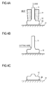
- Figs. 4A to 4C show a method of forming a bump by such ball bonding.
- Fig. 4A shows the state in which a ball 12 formed by the melting of a tip of a metal wire 11 is secured to an electrode 22 of an IC chip 21 by thermocompression bonding.
- the ball 12 is loaded by a ball bonding capillary 31, subjected to thermocompression bonding, and deformed as shown in Fig. 4A .
- the metal wire 11 is cut as shown in Fig. 4B to remove excess parts of the wire 11.
- a bump 12' is formed on the electrode 22 of the IC chip 21 as shown in Fig. 4C .
- Figs. 5A to 5C show flip-chip mounting of the IC chip 21 on which the bump 12' is formed as described above, on the substrate 41. As shown in Fig. 5A , the IC chip 21 is secured to and held by a flip-chip bonding tool 32.
- the Cu electrode 42 of the substrate 41 on which the IC chip 21 is flip-chip-mounted includes Cu (copper) and, in this example, the Cu electrode 42 is coated with Au (gold) to form an Au electrode 43.
- Fig. 5B shows the state in which the flip-chip bonding tool 32 moves (for example, goes down) and the bump 12' is aligned with and brought into contact with the Au electrode 43 of the substrate 41. If, for example, heat and load is applied in the state shown in Fig. 5B , the bump 12' and the Au electrode 43 are bonded to each other. Then, the flip-chip bonding tool 32 is removed to complete the flip-chip mounting. The completed flip-chip mounting structure is shown in Fig. 5C .
- the bonding between the bump 12' and the Au electrode 43 is not limited to thermocompression bonding; for example, ultrasonic bonding, in which ultrasonic vibration is applied under a load, may be used.
- an Al (aluminum) electrode is generally used as the Al electrode 22 of the IC chip 21.
- An Au wire, which is appropriate for ball bonding, is generally used as the metal wire 11 from which the ball 12 is formed (see patent literature 1, for example).
- Patent literature 1 Japanese Patent Application Laid Open No. 2002-368039
- the present invention addresses this problem with the object of providing a flip-chip mounting structure and a flip-chip mounting method that can obtain high connection reliability and bonding reliability even in high temperature.
- a flip-chip mounting structure for wireless connection has an integrated circuit chip having an aluminum electrode and a substrate having a gold electrode, in which the aluminum electrode of the integrated circuit chip and the gold electrode of the substrate are bonded to each other via a bump of aluminum or aluminum alloy formed on the aluminum electrode of the integrated circuit chip.
- a flip-chip method for wirelessly connecting an integrated circuit chip having an aluminum electrode and a substrate having a gold electrode to each other includes the step of performing wedge bonding of a wire made of aluminum or aluminum alloy on the aluminum electrode of the integrated circuit chip by adding supersonic vibration with a wedge bonding capillary, the step of forming a bump by cutting and removing an excess part of the wire subjected to wedge bonding, and the step of aligning the aluminum electrode of the integrated circuit chip on which the bump has been formed with the gold electrode of the substrate, applying pressure, and adding supersonic vibration to bond the aluminum electrode and the gold electrode together.
- the amount of Al can be increased in the flip-chip mounting with the Al/Au bonding structure. Accordingly, one-sided diffusion of Al into Au is not caused, thereby suppressing the generation of voids in the Al electrode of an IC chip, which occurred conventionally. This achieves the high connection reliability and bonding reliability even in high temperature. In other words, it is possible to obtain a superior flip-chip mounting structure with a tolerance against vibration and impact that does not degrade even in exposure to high temperature for extended period of time.
- the bump formed on the Al electrode of the IC chip is an Al bump, not an Au bump.
- Wedge bonding is used to form an Al bump because ball bonding, which is used to form Au bumps, is not appropriate for the forming of an Al bump.
- ball bonding is not appropriate for the forming of an Al bump.
- the first reason is that the height of a tip of an Al bump tends to become uneven when the Al bump is formed by ball bonding since Al is harder than Au.
- the second reason is that Al undergoes oxidation in ball bonding, which forms balls by thermal melting, since Al easily undergoes thermal oxidation. Any of these can cause a serious failure.
- Figs. 1A to 1C show the method of forming an Al bump by wedge bonding.
- Fig. 1A shows the state in which the tip of the Al wire 51 is positioned on the Al electrode 22 of the IC chip 21.
- the Al wire 51 is secured to the Al electrode 22 by applying a load to the Al wire 51 with a wedge bonding capillary 33 and adding supersonic vibration (s1).
- the Al wire 51 is cut as shown in Fig. 1B .
- the Al wire 51 is cut by, for example, holding the Al wire 51 with a clamp 61 and pulling the Al wire 51. This cuts and removes the excess part of the Al wire 51 (s2).
- the Al bump 52 is formed on the Al electrode 22 as shown in Fig. 1C .
- Figs. 2A to 2C show the method for flip-chip mounting of the IC chip 21 on which the Al bump 52 was formed, onto the substrate 41.
- the IC chip 21 is secured to the flip-chip bonding tool 32 as shown in Fig. 2A and then the flip-chip mounting is performed.
- Fig. 2B shows the state in which the flip-chip bonding tool 32 moves (for example, goes down) and the Al bump 52 is aligned with and brought into contact with the Au electrode 43 of the substrate 41.
- the flip-chip bonding tool 32 applies a load and adds supersonic vibration to the Al bump 52 and the Au electrode 43 to bond the Al bump 52 and the Au electrode 43 together.
- Fig. 2C shows the state in which the flip-chip bonding tool 32 is removed and the flip-chip mounting is completed.
- the Al bump 52 is formed on the Al electrode 22 of the IC chip 21 and the Al electrode 22 of the IC chip 21 is bonded to the Au electrode 43 of the substrate 41 via the Al bump 52 as shown (s3). Accordingly, the amount of Al can be increased greatly in the flip-chip mounting with the Al/Au bonding structure.
- one-sided diffusion of Al into Au is not caused, thereby suppressing the generation of voids in the Al electrode 22, which occurred conventionally.
- This achieves high connection reliability and bonding reliability even in high temperature. More specifically, it is possible to achieve a bonding strength in which a tolerance against vibration and impact can be maintained without being degraded even in exposure to high temperature of two hundreds and several tens of degrees Celsius for thousands of hours. This enables the flip-chip mounting of the IC chip 21 assumed to be used in such high temperature and contributes to the downsizing of the substrate (mounting substrate) 41.
- the size of the Al bump 52 is exemplified by a length in the electrode surface direction of not greater than approximately 100 ⁇ m and a thickness of approximately 5 to 50 ⁇ m.
- the wire used to form the Al bump 52 is the Al wire 51, but it may be a wire made of Al alloy. That is, the Al bump 52 may be an Al alloy bump.
- wedge bonding capillary 33 may be any form of tool that can carry out wedge bonding properly.
Landscapes
- Engineering & Computer Science (AREA)
- Manufacturing & Machinery (AREA)
- Microelectronics & Electronic Packaging (AREA)
- Wire Bonding (AREA)
Abstract
Description
- The present invention relates to a flip-chip mounting structure and a flip-chip mounting method of an integrated circuit (IC) chip.
- In flip-chip mounting of an IC chip, generally, a bump is formed on an electrode of the IC chip and the bump is directly bonded to an electrode on a corresponding substrate (mounting substrate). Generally, the bump is formed by ball bonding in which a tip of a metal wire is melted to form a ball and the ball is secured to the electrode of the IC chip by thermocompression bonding etc.
-
Figs. 4A to 4C show a method of forming a bump by such ball bonding.Fig. 4A shows the state in which aball 12 formed by the melting of a tip of ametal wire 11 is secured to anelectrode 22 of anIC chip 21 by thermocompression bonding. Theball 12 is loaded by a ball bonding capillary 31, subjected to thermocompression bonding, and deformed as shown inFig. 4A . - The
metal wire 11 is cut as shown inFig. 4B to remove excess parts of thewire 11. A bump 12' is formed on theelectrode 22 of theIC chip 21 as shown inFig. 4C . -
Figs. 5A to 5C show flip-chip mounting of theIC chip 21 on which the bump 12' is formed as described above, on thesubstrate 41. As shown inFig. 5A , theIC chip 21 is secured to and held by a flip-chip bonding tool 32. - The
Cu electrode 42 of thesubstrate 41 on which theIC chip 21 is flip-chip-mounted includes Cu (copper) and, in this example, theCu electrode 42 is coated with Au (gold) to form anAu electrode 43. -
Fig. 5B shows the state in which the flip-chip bonding tool 32 moves (for example, goes down) and the bump 12' is aligned with and brought into contact with theAu electrode 43 of thesubstrate 41. If, for example, heat and load is applied in the state shown inFig. 5B , the bump 12' and theAu electrode 43 are bonded to each other. Then, the flip-chip bonding tool 32 is removed to complete the flip-chip mounting. The completed flip-chip mounting structure is shown inFig. 5C . The bonding between the bump 12' and theAu electrode 43 is not limited to thermocompression bonding; for example, ultrasonic bonding, in which ultrasonic vibration is applied under a load, may be used. - In the flip-chip mounting structure described above, an Al (aluminum) electrode is generally used as the
Al electrode 22 of theIC chip 21. An Au wire, which is appropriate for ball bonding, is generally used as themetal wire 11 from which theball 12 is formed (see patent literature 1, for example). - Patent literature 1: Japanese Patent Application Laid Open No.
2002-368039 - Since an Au bump is formed on the Al electrode of an IC chip in the conventional flip-chip mounting structure of the IC chip as described above, an Al/Au bonding structure is present.
- If a flip-chip mounting component with this type of Al/Au bonding structure is exposed to high temperature, mutual diffusion between Al and Au is promoted. This causes all Al, which is less than Au in amount, to diffuse into Au, possibly generating voids in the Al electrode. The generation of voids causes failed connection or failed bonding between the Al electrode and the Au bump. This significantly degrades the connection reliability and bonding reliability of the flip-chip mounting structure.
- The present invention addresses this problem with the object of providing a flip-chip mounting structure and a flip-chip mounting method that can obtain high connection reliability and bonding reliability even in high temperature.
- According to a first aspect of the present invention, a flip-chip mounting structure for wireless connection has an integrated circuit chip having an aluminum electrode and a substrate having a gold electrode, in which the aluminum electrode of the integrated circuit chip and the gold electrode of the substrate are bonded to each other via a bump of aluminum or aluminum alloy formed on the aluminum electrode of the integrated circuit chip.
- According to a second aspect of the present invention, a flip-chip method for wirelessly connecting an integrated circuit chip having an aluminum electrode and a substrate having a gold electrode to each other, includes the step of performing wedge bonding of a wire made of aluminum or aluminum alloy on the aluminum electrode of the integrated circuit chip by adding supersonic vibration with a wedge bonding capillary, the step of forming a bump by cutting and removing an excess part of the wire subjected to wedge bonding, and the step of aligning the aluminum electrode of the integrated circuit chip on which the bump has been formed with the gold electrode of the substrate, applying pressure, and adding supersonic vibration to bond the aluminum electrode and the gold electrode together.
- According to the present invention, the amount of Al can be increased in the flip-chip mounting with the Al/Au bonding structure. Accordingly, one-sided diffusion of Al into Au is not caused, thereby suppressing the generation of voids in the Al electrode of an IC chip, which occurred conventionally. This achieves the high connection reliability and bonding reliability even in high temperature. In other words, it is possible to obtain a superior flip-chip mounting structure with a tolerance against vibration and impact that does not degrade even in exposure to high temperature for extended period of time.
-
-
Fig. 1A shows the state in which a tip of anAl wire 51 is positioned on theAl electrode 22 of theIC chip 21; -
Fig. 1B shows the state in which theAl wire 51 is cut; -
Fig. 1C shows the state in which anAl bump 52 is formed on theAl electrode 22. -
Fig. 2A shows the state in which theIC chip 21 is secured to the flip-chip banding tool 32; -
Fig. 2B shows the state in which theAl bump 52 is aligned with and brought into contact with theAu electrode 43 of thesubstrate 41; -
Fig. 2C shows the state in which flip-chip mounting is completed. -
Fig. 3 is a flowchart showing a process according to an embodiment. -
Fig. 4A shows the state in which theball 12 formed by the melting of a tip of themetal wire 11 is secured to theelectrode 22 of theIC chip 21 by thermocompression bonding; -
Fig. 4B shows the state in which themetal wire 11 is cut; -
Fig. 4C shows the state in which the bump 12' is formed on theelectrode 22 of theIC chip 21; -
Fig. 5A shows the state in which theIC chip 21 is secured to and held by the flip-chip bonding tool 32; -
Fig. 5B shows the state in which the bump 12' is aligned with and brought into contact with theAu electrode 43 of thesubstrate 41; -
Fig. 5C shows the state in which a flip-chip mounting structure is completed. - An embodiment of the present invention will be described with reference to
Figs. 1 to 3 . - In this example, the bump formed on the Al electrode of the IC chip is an Al bump, not an Au bump. Wedge bonding is used to form an Al bump because ball bonding, which is used to form Au bumps, is not appropriate for the forming of an Al bump. There are the two following reasons why ball bonding is not appropriate for the forming of an Al bump. The first reason is that the height of a tip of an Al bump tends to become uneven when the Al bump is formed by ball bonding since Al is harder than Au. The second reason is that Al undergoes oxidation in ball bonding, which forms balls by thermal melting, since Al easily undergoes thermal oxidation. Any of these can cause a serious failure.
-
Figs. 1A to 1C show the method of forming an Al bump by wedge bonding.Fig. 1A shows the state in which the tip of theAl wire 51 is positioned on theAl electrode 22 of theIC chip 21. TheAl wire 51 is secured to theAl electrode 22 by applying a load to theAl wire 51 with awedge bonding capillary 33 and adding supersonic vibration (s1). - The
Al wire 51 is cut as shown inFig. 1B . TheAl wire 51 is cut by, for example, holding theAl wire 51 with aclamp 61 and pulling theAl wire 51. This cuts and removes the excess part of the Al wire 51 (s2). TheAl bump 52 is formed on theAl electrode 22 as shown inFig. 1C . -
Figs. 2A to 2C show the method for flip-chip mounting of theIC chip 21 on which theAl bump 52 was formed, onto thesubstrate 41. TheIC chip 21 is secured to the flip-chip bonding tool 32 as shown inFig. 2A and then the flip-chip mounting is performed. -
Fig. 2B shows the state in which the flip-chip bonding tool 32 moves (for example, goes down) and theAl bump 52 is aligned with and brought into contact with theAu electrode 43 of thesubstrate 41. In the state shown inFig. 2B , the flip-chip bonding tool 32 applies a load and adds supersonic vibration to theAl bump 52 and theAu electrode 43 to bond theAl bump 52 and theAu electrode 43 together.Fig. 2C shows the state in which the flip-chip bonding tool 32 is removed and the flip-chip mounting is completed. - In this example, the
Al bump 52 is formed on theAl electrode 22 of theIC chip 21 and theAl electrode 22 of theIC chip 21 is bonded to theAu electrode 43 of thesubstrate 41 via theAl bump 52 as shown (s3). Accordingly, the amount of Al can be increased greatly in the flip-chip mounting with the Al/Au bonding structure. - In this example, one-sided diffusion of Al into Au is not caused, thereby suppressing the generation of voids in the
Al electrode 22, which occurred conventionally. This achieves high connection reliability and bonding reliability even in high temperature. More specifically, it is possible to achieve a bonding strength in which a tolerance against vibration and impact can be maintained without being degraded even in exposure to high temperature of two hundreds and several tens of degrees Celsius for thousands of hours. This enables the flip-chip mounting of theIC chip 21 assumed to be used in such high temperature and contributes to the downsizing of the substrate (mounting substrate) 41. - The size of the
Al bump 52 is exemplified by a length in the electrode surface direction of not greater than approximately 100 µm and a thickness of approximately 5 to 50 µm. - In the above example, the wire used to form the
Al bump 52 is theAl wire 51, but it may be a wire made of Al alloy. That is, theAl bump 52 may be an Al alloy bump. - In addition, the
wedge bonding capillary 33 may be any form of tool that can carry out wedge bonding properly. - The present invention is not limited to the above embodiment and may be modified as appropriate without departing from the scope of the invention.
-
- 11
- Metal wire
- 12
- Ball
- 12'
- Bump
- 21
- IC chip
- 22
- Al electrode
- 31
- Ball bonding capillary
- 32
- Flip-chip bonding tool
- 33
- Wedge bonding capillary
- 41
- Substrate
- 42
- Cu electrode
- 43
- Au electrode
- 51
- Al wire
- 52
- Al bump
Claims (2)
- A flip-chip mounting structure for wireless connection, comprising:an integrated circuit chip having an aluminum electrode; anda substrate having a gold electrode;wherein the aluminum electrode of the integrated circuit chip and the gold electrode of the substrate are bonded to each other via a bump of aluminum or aluminum alloy formed on the aluminum electrode of the integrated circuit chip.
- A flip-chip mounting method for wirelessly connecting an integrated circuit chip having an aluminum electrode and a substrate having a gold electrode to each other, the method comprising the steps of:performing wedge bonding of a wire made of aluminum or aluminum alloy on the aluminum electrode of the integrated circuit chip by adding supersonic vibration with a wedge bonding capillary;forming a bump by cutting and removing an excess part of the wire subjected to wedge bonding; andaligning the aluminum electrode of the integrated circuit chip on which the bump has been formed with the gold electrode of the substrate, applying pressure, and adding supersonic vibration to bond the aluminum electrode and the gold electrode together.
Applications Claiming Priority (2)
| Application Number | Priority Date | Filing Date | Title |
|---|---|---|---|
| JP2010013411A JP2011151322A (en) | 2010-01-25 | 2010-01-25 | Flip-chip mounting structure and flip-chip mounting method |
| PCT/JP2011/050817 WO2011090049A1 (en) | 2010-01-25 | 2011-01-19 | Flip-chip mounting structure and flip-chip mounting method |
Publications (2)
| Publication Number | Publication Date |
|---|---|
| EP2530708A1 true EP2530708A1 (en) | 2012-12-05 |
| EP2530708A4 EP2530708A4 (en) | 2014-01-22 |
Family
ID=44306851
Family Applications (1)
| Application Number | Title | Priority Date | Filing Date |
|---|---|---|---|
| EP11734655.1A Withdrawn EP2530708A4 (en) | 2010-01-25 | 2011-01-19 | BALL CONNECTION STRUCTURE AND BALL CONNECTION METHOD |
Country Status (5)
| Country | Link |
|---|---|
| US (1) | US20120273942A1 (en) |
| EP (1) | EP2530708A4 (en) |
| JP (1) | JP2011151322A (en) |
| CA (1) | CA2786882C (en) |
| WO (1) | WO2011090049A1 (en) |
Families Citing this family (2)
| Publication number | Priority date | Publication date | Assignee | Title |
|---|---|---|---|---|
| KR102245825B1 (en) | 2014-09-04 | 2021-04-30 | 삼성전자주식회사 | Semiconductor pakage |
| JP6538596B2 (en) | 2016-03-14 | 2019-07-03 | 東芝メモリ株式会社 | METHOD FOR MANUFACTURING ELECTRONIC COMPONENT AND APPARATUS FOR MANUFACTURING ELECTRONIC COMPONENT |
Family Cites Families (10)
| Publication number | Priority date | Publication date | Assignee | Title |
|---|---|---|---|---|
| JPH02237119A (en) * | 1989-03-10 | 1990-09-19 | Nippon Steel Corp | Formation of bump electrode |
| JPH09321089A (en) * | 1996-05-29 | 1997-12-12 | Matsushita Electric Works Ltd | Flip chip mounting method |
| JPH10163258A (en) * | 1996-12-03 | 1998-06-19 | Fujitsu Ten Ltd | Bump, bump forming method and bump forming apparatus |
| JPH1174299A (en) * | 1997-08-28 | 1999-03-16 | Sony Corp | Bump forming apparatus and bump forming method |
| JP3590603B2 (en) * | 2000-11-02 | 2004-11-17 | 新日本製鐵株式会社 | Semiconductor device and manufacturing method thereof |
| JP2002261190A (en) * | 2001-02-28 | 2002-09-13 | Sony Corp | Semiconductor device, method of manufacturing the same, and electronic equipment |
| JP2002368039A (en) | 2001-06-07 | 2002-12-20 | Fuji Electric Co Ltd | Flip chip mounting structure and manufacturing method thereof |
| KR100604334B1 (en) * | 2003-11-25 | 2006-08-08 | (주)케이나인 | Flip Chip Bondig Method for Enhancing the Performance of Connection in Flip Chip Packaging Process |
| JPWO2006061879A1 (en) * | 2004-12-06 | 2008-06-05 | 株式会社ルネサステクノロジ | Ignition device, semiconductor device and manufacturing method thereof |
| JP4989437B2 (en) * | 2007-12-14 | 2012-08-01 | ルネサスエレクトロニクス株式会社 | Manufacturing method of semiconductor device |
-
2010
- 2010-01-25 JP JP2010013411A patent/JP2011151322A/en active Pending
-
2011
- 2011-01-19 CA CA2786882A patent/CA2786882C/en not_active Expired - Fee Related
- 2011-01-19 EP EP11734655.1A patent/EP2530708A4/en not_active Withdrawn
- 2011-01-19 WO PCT/JP2011/050817 patent/WO2011090049A1/en not_active Ceased
- 2011-01-19 US US13/520,159 patent/US20120273942A1/en not_active Abandoned
Also Published As
| Publication number | Publication date |
|---|---|
| JP2011151322A (en) | 2011-08-04 |
| WO2011090049A1 (en) | 2011-07-28 |
| US20120273942A1 (en) | 2012-11-01 |
| EP2530708A4 (en) | 2014-01-22 |
| CA2786882A1 (en) | 2011-07-28 |
| CA2786882C (en) | 2015-11-24 |
Similar Documents
| Publication | Publication Date | Title |
|---|---|---|
| JP4262672B2 (en) | Semiconductor device and manufacturing method thereof | |
| KR100998115B1 (en) | Semiconductor device, connection structure and manufacturing method thereof | |
| US7573139B2 (en) | Packed system of semiconductor chips having a semiconductor interposer | |
| EP2232964B1 (en) | Method for forming piercing bond structures on a substrate | |
| US20080122050A1 (en) | Semiconductor Device And Production Method For Semiconductor Device | |
| KR102574011B1 (en) | Mounting structure of semiconductor device and combination of semiconductor device and substrate | |
| KR101934595B1 (en) | Method of mounting semiconducor device | |
| JPH10163213A (en) | Semiconductor device manufacturing method and semiconductor device mounting method | |
| JP2011187635A (en) | Semiconductor device, and method of manufacturing the same | |
| CA2786882C (en) | Flip-chip mounting structure and flip-chip mounting method | |
| JP2009009994A (en) | Semiconductor device and manufacturing method thereof | |
| JP2006179570A (en) | Manufacturing method of semiconductor device | |
| JP2003158140A (en) | Semiconductor package, method of manufacturing semiconductor package, module, and electronic device | |
| JP5187341B2 (en) | Manufacturing method of semiconductor device | |
| JP2014082526A (en) | Method for manufacturing electronic apparatus | |
| JP2016001752A (en) | Flip chip mounting structure, flip chip mounting method, and method of using flip chip mounting structure | |
| JP2019054115A (en) | Manufacturing method of semiconductor device | |
| JP4200090B2 (en) | Manufacturing method of semiconductor device | |
| US20140041918A1 (en) | Looped Interconnect Structure | |
| JP4378227B2 (en) | Flip chip mounting method | |
| JP2010186926A (en) | Method of manufacturing semiconductor device, and semiconductor device | |
| JP2000223534A (en) | Semiconductor mounting apparatus and semiconductor chip mounting method | |
| JP5065657B2 (en) | Electronic device and manufacturing method thereof | |
| TW201901825A (en) | Semiconductor device manufacturing method and semiconductor device | |
| JP2011014757A (en) | Multilayer semiconductor device |
Legal Events
| Date | Code | Title | Description |
|---|---|---|---|
| PUAI | Public reference made under article 153(3) epc to a published international application that has entered the european phase |
Free format text: ORIGINAL CODE: 0009012 |
|
| 17P | Request for examination filed |
Effective date: 20120827 |
|
| AK | Designated contracting states |
Kind code of ref document: A1 Designated state(s): AL AT BE BG CH CY CZ DE DK EE ES FI FR GB GR HR HU IE IS IT LI LT LU LV MC MK MT NL NO PL PT RO RS SE SI SK SM TR |
|
| DAX | Request for extension of the european patent (deleted) | ||
| A4 | Supplementary search report drawn up and despatched |
Effective date: 20140103 |
|
| RIC1 | Information provided on ipc code assigned before grant |
Ipc: H01L 23/485 20060101AFI20131218BHEP Ipc: H01L 21/60 20060101ALI20131218BHEP |
|
| STAA | Information on the status of an ep patent application or granted ep patent |
Free format text: STATUS: THE APPLICATION HAS BEEN WITHDRAWN |
|
| 18W | Application withdrawn |
Effective date: 20160711 |