EP2525484B1 - Spannungsumrichter mit 2n+1 Spannungsstufen - Google Patents
Spannungsumrichter mit 2n+1 Spannungsstufen Download PDFInfo
- Publication number
- EP2525484B1 EP2525484B1 EP12168169.6A EP12168169A EP2525484B1 EP 2525484 B1 EP2525484 B1 EP 2525484B1 EP 12168169 A EP12168169 A EP 12168169A EP 2525484 B1 EP2525484 B1 EP 2525484B1
- Authority
- EP
- European Patent Office
- Prior art keywords
- switching
- voltage
- diode
- transistor
- udc
- Prior art date
- Legal status (The legal status is an assumption and is not a legal conclusion. Google has not performed a legal analysis and makes no representation as to the accuracy of the status listed.)
- Revoked
Links
- 230000002457 bidirectional effect Effects 0.000 claims description 10
- 239000003990 capacitor Substances 0.000 description 72
- 238000006243 chemical reaction Methods 0.000 description 53
- 235000021183 entrée Nutrition 0.000 description 4
- 238000010586 diagram Methods 0.000 description 3
- 230000000737 periodic effect Effects 0.000 description 2
- 241001080024 Telles Species 0.000 description 1
- 230000000295 complement effect Effects 0.000 description 1
- 238000007599 discharging Methods 0.000 description 1
- 238000002347 injection Methods 0.000 description 1
- 239000007924 injection Substances 0.000 description 1
- 238000009413 insulation Methods 0.000 description 1
- 238000002955 isolation Methods 0.000 description 1
Images


Classifications
-
- H—ELECTRICITY
- H02—GENERATION; CONVERSION OR DISTRIBUTION OF ELECTRIC POWER
- H02M—APPARATUS FOR CONVERSION BETWEEN AC AND AC, BETWEEN AC AND DC, OR BETWEEN DC AND DC, AND FOR USE WITH MAINS OR SIMILAR POWER SUPPLY SYSTEMS; CONVERSION OF DC OR AC INPUT POWER INTO SURGE OUTPUT POWER; CONTROL OR REGULATION THEREOF
- H02M7/00—Conversion of AC power input into DC power output; Conversion of DC power input into AC power output
- H02M7/42—Conversion of DC power input into AC power output without possibility of reversal
- H02M7/44—Conversion of DC power input into AC power output without possibility of reversal by static converters
- H02M7/48—Conversion of DC power input into AC power output without possibility of reversal by static converters using discharge tubes with control electrode or semiconductor devices with control electrode
- H02M7/483—Converters with outputs that each can have more than two voltages levels
- H02M7/487—Neutral point clamped inverters
-
- H—ELECTRICITY
- H02—GENERATION; CONVERSION OR DISTRIBUTION OF ELECTRIC POWER
- H02M—APPARATUS FOR CONVERSION BETWEEN AC AND AC, BETWEEN AC AND DC, OR BETWEEN DC AND DC, AND FOR USE WITH MAINS OR SIMILAR POWER SUPPLY SYSTEMS; CONVERSION OF DC OR AC INPUT POWER INTO SURGE OUTPUT POWER; CONTROL OR REGULATION THEREOF
- H02M7/00—Conversion of AC power input into DC power output; Conversion of DC power input into AC power output
- H02M7/42—Conversion of DC power input into AC power output without possibility of reversal
- H02M7/44—Conversion of DC power input into AC power output without possibility of reversal by static converters
- H02M7/48—Conversion of DC power input into AC power output without possibility of reversal by static converters using discharge tubes with control electrode or semiconductor devices with control electrode
- H02M7/483—Converters with outputs that each can have more than two voltages levels
- H02M7/4837—Flying capacitor converters
-
- H—ELECTRICITY
- H02—GENERATION; CONVERSION OR DISTRIBUTION OF ELECTRIC POWER
- H02M—APPARATUS FOR CONVERSION BETWEEN AC AND AC, BETWEEN AC AND DC, OR BETWEEN DC AND DC, AND FOR USE WITH MAINS OR SIMILAR POWER SUPPLY SYSTEMS; CONVERSION OF DC OR AC INPUT POWER INTO SURGE OUTPUT POWER; CONTROL OR REGULATION THEREOF
- H02M1/00—Details of apparatus for conversion
- H02M1/0095—Hybrid converter topologies, e.g. NPC mixed with flying capacitor, thyristor converter mixed with MMC or charge pump mixed with buck
Definitions
- the present invention relates in particular to voltage inverters at 2N + 1 levels, where N is an integer with a value greater than or equal to 2.
- Such voltage inverters with a high number of output voltage levels have several advantages over voltage inverters with two or three levels, such as a reduction of the harmonic distortion of the output AC voltage and a reduction of insulation stresses at the level of the electric motor intended to be supplied by the inverter.
- the present invention applies in particular to conversion systems having a high electrical power, such as a power greater than 100kW.
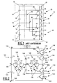
- the figure 1 illustrates such a conversion system.
- the conversion system 10 is a voltage inverter with five output levels, and has two input terminals 12, four capacitors 14 connected in series between the input terminals 12 and connected together in pairs by a midpoint 16 respectively.
- the conversion system 10 also comprises, for the or each phase of the output voltage, an output terminal 18 and two switching branches 20 each connected between the output terminal 18 and a respective input terminal 12.
- Each switching branch comprises four switching cells 22 connected in series and three intermediate points 24, the switching cells 22 being successively interconnected by an intermediate point 24 corresponding.
- the conversion system 10 also comprises three intermediate branches 26 each connected to a respective midpoint 16 and comprising two diodes 28, 30.
- the first diode 28 is connected in direct contact between the said midpoint 16 and a corresponding intermediate point of one of the two switching branches 20, the second diode 30 being connected in reverse between said respective midpoint 16 and an intermediate point 24 of the other of the two switching branches 20.
- the conversion system 10 also comprises means, not shown, of control of switching cells 22.
- the conversion system then generally comprises means for balancing the voltage across each of the capacitors, such as balancing means by adding a common-mode zero sequence component on each of the phases of the output AC current, the offset between phases for charging or discharging the capacitors.
- balancing means are effective when the amplitude of the output AC voltage is less than a limit value substantially equal to one quarter of the value of the DC input voltage, and do not allow correct balancing when the amplitude of the output AC current is greater than said value.
- balancing means cause overcharge.
- the aim of the invention is to propose a conversion system making it possible to reduce the voltage unbalance at the mid-points, whatever the voltage and the current delivered by the conversion system, while not requiring additional balancing means. the voltage across the capacitors.
- the present invention relates to a system for converting an input DC voltage into an output AC voltage comprising at least one phase and having 2N + 1 levels, where N is an integer greater than or equal to 2.
- the system for example, a voltage inverter at 2N + 1 levels.
- the AC voltage is, for example, periodic.
- the conversion system is intended to supply a load with a voltage comprising at least one phase and having a high value, for example greater than 1000V.
- the charge has a high electrical power, for example greater than 100kW.
- the load is, for example, a three-phase electric motor.
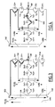
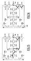
- the figure 2 represents a first embodiment of the conversion system voltage 100 to 2N + 1 levels, with N equal to 2, or five levels.
- the conversion system 100 comprises two input terminals 102, namely a positive terminal denoted E + and a negative terminal denoted E-, and two voltage generators 104 connected in series between the input terminals 102 and interconnected by a midpoint 106, also noted M1.
- the conversion system 100 comprises, for the or each phase of the output voltage, a single phase being represented on the figure 2 , an output terminal 108, also denoted S, and two switching branches 110 each connected between the output terminal 108 and a respective input terminal 102.
- Each switching branch 110 comprises two first switching cells 112 connected in series and an intermediate point 114, the first two cells 112 being interconnected by the intermediate point 114.
- the conversion system 100 further comprises, for the or each phase of the output voltage, a pair of capacitors 116, each pair of capacitors 116 being connected between an intermediate point 114 of one of the two switching branches and an intermediate point 114 of the other two switching branches, the two capacitors 116 of the pair being interconnected by a midpoint 118, also noted M2.
- the conversion system 100 also comprises, for the or each phase of the output voltage, two second switching cells 120, a second cell 120 being connected between the output terminal 108 and the midpoint 118, and the second second cell 120 being connected between the midpoints 106, 118.
- the conversion system 100 comprises means 121 for controlling the first switching cells 112 and the second switching cells 120.
- the conversion system 100 is, for example, a three-phase inverter, and then comprises three output terminals 108, six switching branches 110, three pairs of capacitors 116 and six second switching cells 120.
- the two voltage generators 104 connected between the input terminals 102 are identical, and include, for example, each a capacitor.
- the capacitors of the voltage generators 104 have a capacity of the same value.
- the capacitor connected to the positive input terminal is denoted C1 +, and the capacitor connected to the negative input terminal is denoted C1-.
- the switching branch 110 connected to the positive input terminal E + will thereafter be referred to as the positive switching branch, and the switching branch 110 connected to the negative input terminal E- will thereafter be called the negative switching branch.
- Each first switching cell 112 has at least one first bidirectional current switch 122.
- each first switching cell 112 consists of a first switch 122.
- each first switching cell 112 has a plurality of first switches 122 connected in series with each other.
- the two capacitors 116 of the pair of capacitors connected between the intermediate points 114 are identical, and therefore have a capacity of the same value.
- the capacitor 116 connected to the intermediate point 114 of the positive switching branch is denoted C2 +
- the capacitor 116 connected to the intermediate point 114 of the negative switching branch is denoted C2-.
- Each second switching cell 120 is directional in current and voltage.
- Each second switching cell 120 comprises at least two second switches 124 connected in anti-series, as shown in FIG. figure 2 .
- each second switching cell 120 consists of two second switches 124 connected in anti-series.
- each second switching cell 120 comprises two second switches connected in antiparallel.
- the control means 121 are able to control the switching of the first (s) and second (s) cells 112, 120 corresponding to a control law.
- the control law is such that the current flows, for at least one given value of the output AC voltage, through a corresponding capacitor 116 in one direction during a first phase, then in the other direction during the first phase. a second phase, so as to balance the voltage across the capacitor 116.
- the law control circuit has a switching frequency of the first (s) and second (s) cells 112, 120.
- the first switches 122 of the two switching branches are connected in series and in the same direction between the two input terminals 102.
- Each first switch 122 comprises, for example, a transistor 126 and a diode 128 connected in anti-parallel of the transistor 126.
- each first switch 122 comprises a thyristor and a diode, not shown, the diode being connected in antiparallel to the thyristor.
- Each second switch 124 comprises, when the second switches are anti-series connected in a second switching cell 120, a transistor 130 and a diode 132 connected in anti-parallel of the transistor 130, as shown in FIG. figure 2 .
- each second switch 124 comprises, when the second switches are anti-series connected within a second switching cell 120, a thyristor and a diode, not shown, the diode being connected in antiparallel to the thyristor.
- each second switch comprises, when the second switches are connected in anti-parallel within a second switching cell 120, at least one diode, a transistor connected in series with the diode and another connected diode. in anti-parallel of the transistor.
- each second switch 124 comprises, when the second switches are connected in anti-parallel within a second switching cell 120, a thyristor and a diode, not shown, the diode being connected in series with the thyristor.
- the transistors 126 of the first switches, and the transistors connected in anti-series or antiparallel of the second switches 124 are, for example, transistors IGBT (English Insulated Gate Bipolar Transistor). In a variant, said transistors are IEGT transistors (of the English Injection Enhanced Gate Transistor).
- the thyristors of the first and second switches 122, 124 are Gate Turn-Off (GTO) thyristors or Gate Controlled Thyristor (GCT) thyristors.
- GTO Gate Turn-Off
- GCT Gate Controlled Thyristor
- the transistors 126 of the positive switching branch are respectively denoted T1 +, T2 +, and the transistors 126 of the negative switching branch are respectively denoted T1-, T2-.
- the diodes 128 connected in anti-parallel of the transistors T1 +, respectively T2 +, are denoted D1 +, respectively D2 +.
- the diodes 128 connected in anti-parallel of the transistors T1-, respectively T2-, are denoted D1-, respectively D2-.
- Transistors 130 are identical. The transistors 130 of the same second switching cell 120 are simultaneously controlled by the control means 121.
- the transistors 130 of the second switching cell connected between the mid-points 106, 118 are connected anti-series, and respectively denoted Tc1 + and Tc1-.
- the transistors 130 of the second switching cell connected between the midpoint 118 and the output terminal 108 are also anti-series connected, respectively Tc2 +, Tc2-.
- the diodes 132 connected in anti-parallel of the transistors Tc1 +, respectively Tc1-, are denoted Dc1 +, respectively Dc1-.
- the diodes 132 connected in anti-parallel of the transistors denoted Tc2 +, respectively Tc2-, are denoted Dc2 +, respectively Dc2-.
- the conversion system 100 is bidirectional. In other words, the electric current is able to flow from the input terminals 102 to the output terminal or terminals 108, the conversion system 100 then operating as an inverter, and conversely the current is also able to flow from the terminal or terminals. output 108 to the input terminals 102, the conversion system 100 then operating as a rectifier.
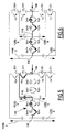
- the Figures 3 to 16 illustrate the conduction sequence of the transistors and diodes of the first switches 122 and the second switches 124 of the conversion system 100 at five levels. More specifically, Figures 3 to 9 illustrate the conduction sequence when the current through the output terminal 108 is positive, i.e. as it flows from a respective input terminal 102 to the output terminal 108. In a complementary manner, the Figures 10 to 16 illustrate the conduction sequence when the current through the output terminal 108 is negative, i.e., as it flows from the output terminal 108 to the respective input terminal 102.
- the DC voltage between input terminals 102 is denoted Udc, as shown in FIG. figure 3 .
- the voltage between the midpoint 106 and the positive input terminal E + is then equal to + Udc / 2
- the voltage between the midpoint 106 and the negative input terminal E- is then equal to -Udc / 2.
- the capacitors 116 are initially loaded at a voltage equal to Udc / 4.
- the voltage between the midpoint 118 and the intermediate point 114 of the positive switching branch is initially equal to + Udc / 4
- the voltage between the midpoint 118 and the intermediate point 114 of the negative switching branch is initially equal to -Udc / 4.
- the Figures 3 to 9 illustrate successive states for which the voltage delivered at the output of the conversion system varies, during a first half-period, from + Udc / 2 to -Udc / 2, in steps of Udc / 4, with the figures 4 and 5 corresponding to the same output voltage equal to + Udc / 4 and the Figures 7 and 8 corresponding to the same output voltage equal to -Udc / 4 depending on whether the current flows in one or the other of the second switching cells 120.
- the variation of the output voltage during the second half-period is obtained by symmetry, the voltage varying from -Udc / 2 to + Udc / 2, in steps of Udc / 4.
- the output voltage delivered is also equal to + Udc / 4, but the current flows in this case from the midpoint 106 to the output terminal 108 through the transistor Tc1 +, the diode Dc1-, the capacitor C2 + and the transistor T1 +.
- the states of figures 4 and 5 are therefore redundant regarding the value of the output voltage.
- the state of the figure 4 corresponds to a positive current through the capacitor C2 +, and the state of the figure 5 corresponds to a negative current through the capacitor C2 +.
- control law is such that the current flows, for the given value + Udc / 4 of the output AC voltage, through the capacitor C2 + in one direction during a first phase represented on the figure 4 , then in the other direction during a second phase represented on the figure 5 .
- the average current through the capacitor C2 + is zero over a balancing period, which makes it possible to reduce the load imbalances at the terminals of this capacitor C2 + and to have a mean voltage across the capacitor C2 + substantially equal to + Udc / 4 between the midpoint 118 and the intermediate point 114 of the positive switching branch.
- the balancing period is, for example, the period of the AC voltage.
- the balancing period is the half-period of the AC voltage.
- the balancing period is the switching period, that is to say the inverse of the switching frequency of the control law.
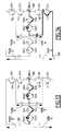
- the output voltage delivered is zero, the current flowing from the midpoint 106 to the output terminal 108 through the transistor Tc1 +, the diode Dc1-, the transistor Tc2 + and the diode Dc2-.
- the current flows from the midpoint 106 to the zero potential across the two second switching cells 120 and without passing through a capacitor 116 so that the voltage is zero.
- the voltage delivered is also equal to -Udc / 4, but the current flows through a different path, from the midpoint 106 to the output terminal 108 through the transistor Tc1 + and the diode Dc1- of the second switching cell. 120 connected between the mid-points 106, 118, the capacitor C2- and the diode D2-.
- control law is such that the current flows, for the given value -Udc / 4 of the output AC voltage, through the capacitor C2- in one direction during a first phase represented on the figure 7 , then in the other direction during a second phase represented on the figure 8 .
- the figure 9 corresponds to the last switching state when the conversion system 100 operates in an inverter and the current flows from an input terminal E +, E- or the midpoint 106 to the output terminal S. On the figure 9 the current flows from the negative input terminal E- to the output terminal S through the diodes D1- and D2-, and the output voltage is equal to -Udc / 2.
- the Figures 10 to 16 illustrate the successive states for which the alternating voltage varies, during a first half-period, from + Udc / 2 to -Udc / 2, in steps of Udc / 4, with the Figures 11 and 12 corresponding to the same alternating voltage equal to + Udc / 4 and the figures 14 and 15 corresponding to the same alternating voltage equal to -Udc / 4 depending on whether the current flows in one or the other of the second switching cells 120.
- the variation of the output voltage during the second half-period is obtained by symmetry, the voltage varying from -Udc / 2 to + Udc / 2, in steps of Udc / 4.
- the current flows from the output terminal 108 to the positive input terminal E + through the second switching cell 120 connected between the midpoint 118 and the output terminal 108 via the transistor Tc2- and the diode Dc2 +, then to through capacitor C2 + and diode D2 +.
- the voltage is then equal to + Udc / 4.
- the voltage is also equal to + Udc / 4, but the current flows in a different path, namely through the diode D1 +, the capacitor C2 + and the second switching cell 120 connected between the mid-points 106, 118, via the transistors Tc1- and diode Dc1 +.
- the state of the figure 12 is therefore redundant from that of the figure 11 relating to the value of the voltage, and the difference between the two states corresponds to the direction of flow of the current through the capacitor C2 +, the current through the capacitor C2 + being positive in the state of the figure 11 and negative in that of the figure 12 .
- control law is such that the current flows, for the given value + Udc / 4 of the alternating voltage, through the capacitor C2 + in one direction during a first phase represented on the figure 11 , then in the other direction during a second phase represented on the figure 12 .
- the current flows from the output terminal 108 to the midpoint 106 at the zero potential across the two second switching cells 120, so that the voltage is zero. More precisely, the current flows through the transistor Tc2- and the diode Dc2 +, then through the transistor Tc1- and the diode Dc1 +.
- the current flows from the output terminal 108 to the negative input terminal E- through the second switching cell 120 connected between the midpoint 118 and the output terminal 108, via the transistor Tc2- and the diode Dc2 +, then through capacitor C2- and transistor T1-.
- the voltage is equal to -Udc / 4.
- the voltage is also equal to -Udc / 4 but the path followed by the current is different, the latter flowing through the transistor T2-, the capacitor C2- and the second switching cell 120 connected between the midpoints 106, 118, via the transistor Tc1- and the diode Dc1 +, from the output terminal 108 to the midpoint 106.
- the state of the figure 15 is also redundant from that of the figure 14 , and the difference between the two states corresponds to the flow direction of the current through the capacitor C2-, the current flowing in the capacitor C2- being positive in the state of the figure 14 and negative in that of the figure 15 .
- control law is such that the current flows, for the given value -Udc / 4 of the alternating voltage, through the capacitor C2- in one direction during a first phase represented on the figure 14 , then in the other direction during a second phase represented on the figure 15 .
- first and second switches 122, 124 comprise thyristors.
- the bidirectional conversion system 100 thus makes it possible to deliver a voltage with five levels in the exemplary embodiment of FIGS. Figures 2 to 16 , where the values taken by the alternating voltage are equal to + Udc / 2, + Udc / 4, 0, -Udc / 4, or -Udc / 2, the DC voltage being equal to Udc.
- the conversion system according to the invention makes it possible to reduce the imbalances of charges at the mid-point 118, by the state redundancies for the + Udc / 4 and -Udc / 4 voltages making it possible to have a zero average current at through capacitors C2 + and C2- over the balancing period.
- the conversion system also makes it possible to have an average voltage across the capacitor C2 + substantially equal to + Udc / 4 between the midpoint 118 and the intermediate point 114 of the positive switching branch, and a mean voltage across the capacitor C2. -sensively equal to -Udc / 4 between the midpoint 118 and the intermediate point 114 of the negative switching branch.
- the control law is such that the state redundancies for voltages + Udc / 4 and -Udc / 4 occur during each half-period of the AC voltage.
- the balancing period is the half-period of the AC voltage.
- the control law is such that the state redundancies for the + Udc / 4 and -Udc / 4 voltages occur during the period of the alternating voltage, a first state being implemented during the first half-period, and the corresponding redundant state being implemented during the second half-period.
- the balancing period is the period of the AC voltage.
- each first switching cell 112 comprises a plurality of first switches 122 makes it possible to deliver an output voltage of greater value.
- each first switching cell 112 includes a plurality of first switches 122 allows the use of components, i.e., transistors and diodes, having a voltage of 100. lower use. Such components with lower operating voltage are less expensive.
- the second switch cells 120 do not have an electromagnetic coil. In other words, no electromagnetic coil is connected between the midpoints M1 and M2 or between the midpoint M2 and the output terminal 108.
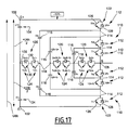
- FIG 17 illustrates a second embodiment of the invention for which the elements similar to the first embodiment, described above, are identified by identical references, and are not described again.
- the conversion system 100 has 2N + 1 levels, where N is an integer greater than or equal to 2.
- the conversion system 100 is, for example, a voltage inverter at 2N + 1 levels.
- the second embodiment is a generalization of the first embodiment for which N was equal to 2.
- the conversion system 100 comprises two input terminals 102, ie a positive terminal E + and a negative terminal E-, and two voltage generators 104 connected in series between the input terminals 102 and connected together by a midpoint 106.
- the conversion system 100 includes, for the or each phase of the output voltage, an output terminal 108 and two switching branches 110 each connected between the output terminal 108 and a respective input terminal 102.
- Each switching branch 110 has N first switching cells 112 connected in series and N-1 intermediate points 114, the first switching cells 112 being successively interconnected by a corresponding intermediate point 114.
- the conversion system 100 also comprises, for the or each phase of the output voltage, N-1 pair (s) of capacitors 116, each pair of capacitors 116 being connected between an intermediate point 114 of one of the two switching branches. 110 and an intermediate point 114 of the other of the two switching branches 110, and the two capacitors 116 of each pair being interconnected by a midpoint 118.
- the conversion system 100 also includes, for the or each phase of the output voltage, N second switching cells 120, one of the N second cells 120 being connected between the output terminal 108 and a midpoint 118, and each N-1 other second cell (s) 120 being connected between two midpoints 106, 118.
- the conversion system 100 comprises means 121 for controlling the first and second switching cells 112, 120.
- Each first switching cell 112 comprises at least one first bidirectional switch 122. In a variant, each first switching cell 112 comprises a plurality of first switches 122.
- Each second switching cell 120 is bidirectional in current and voltage.
- Each second switching cell 120 comprises at least two second switches 124 connected in anti-series, as shown in FIG. figure 17 .
- each second switching cell 120 consists of two second switches 124 connected in anti-series.
- each second switching cell 120 comprises a plurality of pairs of second switches 124 connected in anti-series.
- each second switching cell 120 comprises two second switches connected in antiparallel.
- the control means 121 are able to control the switching of the first (s) and second (s) cells 112, 120 corresponding to a control law.
- the control law is such that the current flows, for at least one given value of the output AC voltage, through a corresponding capacitor 116 in one direction during a first phase, then in the other direction during the first phase. a second phase.
- the control law has a switching frequency of the first (s) and second (s) cells 112, 120.
- the average current through the corresponding capacitor 116 is zero over a balancing period, which makes it possible to reduce the load imbalances at the terminals of the corresponding capacitor 116 and to have a mean voltage across the corresponding substantially equal capacitor 116. at Udc / 4 in absolute value.
- the control law is, for example, such that the first phase and the second phase are included in each half-period of the AC voltage, the latter being periodic.
- the balancing period is the half-period of the AC voltage.
- control law is such that the first phase is included in the first half-period of the AC voltage, and the second phase is included in the second half-period.
- the balancing period is the period of the AC voltage.
- the balancing period is the switching period, that is to say the inverse of the switching frequency of the control law.
- Each first switch 122 comprises a transistor 126 and a diode 128 connected in anti-parallel of the transistor 126.
- the transistors 126 are denoted Ti + and the corresponding diodes 128 are denoted Di +, the index i varying between 1 and N in the example of realization of the figure 17 wherein each first switching cell 112 consists of a first bidirectional switch 122.
- each first switch 122 comprises a thyristor and a diode, not shown, the diode being connected in anti-parallel of the thyristor.
- Each second switch 124 comprises a transistor 130 and a diode 132 connected in anti-parallel of the transistor 130 when the second switches 124 of each switching cell 120 are connected in anti-series.
- the two transistors 130 of each second switching cell are then connected in anti-series and noted Tci +, Tci-, the index i varying between 1 and N in the embodiment of the figure 17 where each second switching cell 120 consists of two second switches 124 connected in anti-series.
- the diodes 132 are denoted Dci +, Dci-, the index i also varying between 1 and N.
- each second switch 124 comprises, when the second switches are anti-series connected in a second cell. switch 120, a thyristor and a diode, not shown, the diode being connected in anti-parallel of the thyristor.
- each second switch comprises at least one diode, a transistor connected in series with the diode and another diode connected in anti-parallel of the transistor, not shown, when the second switches of each second switching cell are connected. in anti-parallel.
- each second switch 124 comprises, when the second switches are connected in anti-parallel within a second switching cell 120, a thyristor and a diode, not shown, the diode being connected in series of the thyristor.
- the DC voltage between the input terminals 102 is equal to Udc, and the voltage across the capacitor C1 + between the midpoint 106 and the positive input terminal.
- E + is then equal to + Udc / 2, the voltage across the capacitor C1- between the midpoint 106 and the negative input terminal E- being equal to -Udc / 2.
- This second embodiment has state redundancies with the circulating current, for the same value of the alternating voltage, in one direction and then in the other, through each of the capacitors 116 denoted Ci +, respectively Ci , N-1 pair (s) of capacitors, i being between 2 and N.
- control law is such that the current flows, for the given value + (N + 1-i) xUdc / 2N, respectively - (N + 1-i) xUdc / 2N, of the alternating voltage, through the capacitor Ci +, respectively Ci-, in one direction during a first phase, then in the other direction during a second phase, i varying between 2 and N, and N being an integer greater than or equal to 2.
- the average current through each of the capacitors 116 of the N-1 pair (s) of capacitors is zero over the balancing period due to the redundancies of states.
- the average voltage across each of the capacitors 116 of the i th pair of capacitors is substantially equal to (N + 1-i) xUdc / 2N in absolute value, i being between 2 and N.
- the second switch cells 120 do not have an electromagnetic coil. In other words, no electromagnetic coil is connected between the midpoints 116, 118 or between the midpoint 118 and the output terminal 108.
- the conversion system 100 makes it possible to reduce the voltage unbalance at mid-points regardless of the voltage and the voltage. current delivered by the conversion system, while not requiring additional means of balancing the voltage across the capacitors.
Landscapes
- Engineering & Computer Science (AREA)
- Power Engineering (AREA)
- Inverter Devices (AREA)
Claims (9)
- System zur Wandlung einer Eingangsgleichspannung in eine Ausgangswechselspannung mit wenigstens einer Phase, aufweisend:- zwei Eingangsanschlüsse (102),- zwei Spannungsquellen (104) die zwischen den Eingangsschlüssen (102) in Reihe geschaltet sind und miteinander über einen ersten Mittelpunkt (106) verbunden sind,für die oder jede Phase der Ausgangsspannung:- einen Ausgangsanschluss (108),- zwei Schaltzweige (110), die jeweils zwischen einen der Eingangsanschlüsse (102) und den Ausgangsanschluss (108) geschaltet sind, wobei jeder Schaltzweig (110) N erste in Reihe geschaltete Schaltzellen (112) und N-1 Zwischenpunkte (114) aufweist, wobei die ersten Schaltzellen (112) sukzessiv über einen entsprechenden Zwischenpunkt (114) miteinander verbunden sind, wobei N eine ganze Zahl größer oder gleich zwei ist,- Steuermittel (121) der ersten Schaltzellen (112), dadurch gekennzeichnet, dass es unter anderem aufweist: für die oder jede Phase der Ausgangsspannung:- N-1 Kondensatorpaare (116), wobei jedes Kondensatorpaar (116) zwischen einen Zwischenpunkt (114) von einem der beiden Schaltzweige (110) und einen Zwischenpunkt (114) vom anderen der beiden Schaltzweige (110) zwischengeschaltet ist, wobei die beiden Kondensatoren (116) jedes Paares miteinander über zweite Mittelpunkte (118) verbunden sind,- N zweite Schaltzellen (120), wobei eine unter den N zweiten Schaltzellen (120) zwischen den Ausgangsanschluss (108) und einen ersten zweiten Mittelpunkt (118) geschaltet ist, und jede der N-1 anderen zweiten Zellen (120) zwischen zwei Mittelpunkte (118, 106) geschaltet ist, und- Steuermittel (121) der zweiten Schaltzellen (120),
und dadurch gekennzeichnet, dass die Steuermittel (121) dazu geeignet sind, das Schalten der entsprechenden ersten und zweiten Zellen (112, 120) gemäß einem Steuergesetz zu steuern, wobei das Steuergesetz derart ist, dass der Strom für wenigstens einen vorgegebenen Wert von +Udc/4 und -Udc/4 der Ausgangswechselspannung über einem zugeordneten Kondensator (116) während einer ersten Phase in eine Richtung und dann während einer zweiten Phase in die andere Richtung fließt. - System (100) nach Anspruch 1, bei dem jede erste Schaltzelle (112) wenigstens einen ersten Schalter (122) aufweist, der für den Strom bidirektional ist.
- System (100) nach Anspruch 2, bei dem die ersten Schalter (122) der beiden Schaltzweige (110) in Reihe und in derselben Richtung zwischen die beiden Eingangsanschlüsse (102) geschaltet sind.
- System (100) nach Anspruch 2 oder 3, bei dem jeder erste Schalter einen Transistor (126) und eine Diode (128) aufweist, die antiparallel zum Transistor (126) geschaltet ist.
- System (100) nach einen der vorhergehenden Ansprüche, bei dem jede zweite Schaltzelle (120) für den Strom und die Spannung bidirektional ist.
- System (100) nach Anspruch 5, bei dem jede zweite Schaltzelle (120) zumindest zwei zweite Schalter (124) aufweist, die antiseriell geschaltet sind.
- System (100) nach Anspruch 6, bei dem jeder zweite Schalter (124) einen Transistor (130) und eine Diode (132) aufweist, die antiparallel zum Transistor (130) geschaltet ist.
- System (100) nach Anspruch 5, bei dem jede zweite Schaltzelle (120) zwei zweite antiparallel geschaltete Schalter aufweist.
- System (100) nach Anspruch 8, bei dem jeder zweite Schalter zumindest eine Diode, einen in Reihe zur Diode geschalteten Transistor und eine weitere zum Transistor antiparallel geschaltete Diode aufweist.
Applications Claiming Priority (1)
| Application Number | Priority Date | Filing Date | Title |
|---|---|---|---|
| FR1154283A FR2975549B1 (fr) | 2011-05-17 | 2011-05-17 | Onduleur de tension a 2n+1 niveaux |
Publications (2)
| Publication Number | Publication Date |
|---|---|
| EP2525484A1 EP2525484A1 (de) | 2012-11-21 |
| EP2525484B1 true EP2525484B1 (de) | 2013-11-27 |
Family
ID=46046040
Family Applications (1)
| Application Number | Title | Priority Date | Filing Date |
|---|---|---|---|
| EP12168169.6A Revoked EP2525484B1 (de) | 2011-05-17 | 2012-05-16 | Spannungsumrichter mit 2n+1 Spannungsstufen |
Country Status (3)
| Country | Link |
|---|---|
| US (1) | US9071165B2 (de) |
| EP (1) | EP2525484B1 (de) |
| FR (1) | FR2975549B1 (de) |
Cited By (1)
| Publication number | Priority date | Publication date | Assignee | Title |
|---|---|---|---|---|
| RU2793273C2 (ru) * | 2018-05-23 | 2023-03-30 | Нидек Аси С.П.А. | Преобразователь электрической энергии |
Families Citing this family (32)
| Publication number | Priority date | Publication date | Assignee | Title |
|---|---|---|---|---|
| CN102255538B (zh) * | 2010-05-19 | 2014-03-12 | 力博特公司 | 一种t型三电平逆变电路 |
| JP6123219B2 (ja) * | 2011-10-14 | 2017-05-10 | 株式会社明電舎 | マルチレベル電力変換器 |
| FR2992116B1 (fr) * | 2012-06-18 | 2015-11-13 | Univ Lorraine | Circuit convertisseur matriciel reversible |
| US9425705B2 (en) | 2012-08-13 | 2016-08-23 | Rockwell Automation Technologies, Inc. | Method and apparatus for bypassing cascaded H-bridge (CHB) power cells and power sub cell for multilevel inverter |
| US9252670B2 (en) * | 2012-12-19 | 2016-02-02 | General Electric Company | Multilevel converter |
| CN103929045B (zh) * | 2013-01-16 | 2019-06-07 | 通用电气能源电能变换科技有限公司 | 变换器装置,驱动单元和相关方法 |
| CN103973128A (zh) * | 2013-01-30 | 2014-08-06 | 通用电气能源电能变换科技有限公司 | 无变压器式电能变换系统以及相关方法 |
| JP6079407B2 (ja) * | 2013-04-22 | 2017-02-15 | 富士電機株式会社 | マルチレベル変換回路 |
| US9083230B2 (en) * | 2013-06-20 | 2015-07-14 | Rockwell Automation Technologies, Inc. | Multilevel voltage source converters and systems |
| CN103354427B (zh) * | 2013-06-24 | 2015-07-08 | 华为技术有限公司 | 一种单相逆变器和三相逆变器 |
| CN104283432B (zh) | 2013-07-03 | 2017-12-26 | 通用电气公司 | 联合共模电压注入系统和方法 |
| CN104601000A (zh) * | 2013-10-31 | 2015-05-06 | 通用电气公司 | 变换器控制器,电能变换系统以及控制方法 |
| US10069430B2 (en) * | 2013-11-07 | 2018-09-04 | Regents Of The University Of Minnesota | Modular converter with multilevel submodules |
| CN104811073B (zh) * | 2014-01-24 | 2019-05-31 | 通用电气能源电能变换科技有限公司 | 变换器模块、装置、系统和相关方法 |
| CN105099241B (zh) * | 2014-04-18 | 2019-03-19 | 通用电气公司 | 控制器、电能变换系统和方法 |
| CN104270025A (zh) * | 2014-09-28 | 2015-01-07 | 中冶赛迪电气技术有限公司 | 一种多电平逆变器及其调制方法 |
| JP6454939B2 (ja) * | 2014-10-29 | 2019-01-23 | パナソニックIpマネジメント株式会社 | 電力変換装置、およびそれを用いたパワーコンディショナ |
| CN105743361B (zh) * | 2014-12-12 | 2018-10-09 | 台达电子工业股份有限公司 | 功率转换器的排布版图 |
| US9595869B2 (en) * | 2015-02-27 | 2017-03-14 | Qualcomm Incorporated | Multi-level switching regulator circuits and methods with finite state machine control |
| DE102015105889A1 (de) * | 2015-04-17 | 2016-10-20 | Ge Energy Power Conversion Technology Limited | Schaltmodul und Umrichter mit wenigstens einem Schaltmodul |
| CN106329974B (zh) * | 2015-07-10 | 2018-12-21 | 台达电子企业管理(上海)有限公司 | 五电平变换装置 |
| FR3060906B1 (fr) * | 2016-12-16 | 2019-05-24 | Ge Energy Power Conversion Technology Limited | Convertisseur continu-alternatif |
| US10404175B2 (en) * | 2017-12-29 | 2019-09-03 | Texas Instruments Incorporated | Converter topology with adaptive power path architecture |
| EP3573227A1 (de) * | 2018-05-23 | 2019-11-27 | Nidec ASI S.A. | Stromwandler |
| FR3081634B1 (fr) * | 2018-05-23 | 2021-02-26 | Nidec Asi | Convertisseur de puissance electrique |
| CN110086365B (zh) * | 2019-05-05 | 2020-07-28 | 北京交通大学 | 一种中点自平衡三电平并网变流器拓扑 |
| EP4024694A1 (de) * | 2020-12-30 | 2022-07-06 | Siemens Aktiengesellschaft | Flying capacitor modul und multilevel-umrichter |
| US11342878B1 (en) | 2021-04-09 | 2022-05-24 | Rockwell Automation Technologies, Inc. | Regenerative medium voltage drive (Cascaded H Bridge) with reduced number of sensors |
| EP4315582A1 (de) * | 2021-04-15 | 2024-02-07 | Huawei Technologies Co., Ltd. | Matrixleistungswandler und verfahren zur verwendung in dem matrixleistungswandler |
| WO2022237979A1 (en) | 2021-05-12 | 2022-11-17 | Huawei Technologies Co., Ltd. | Quasi multi-level converter |
| NL2029114B1 (en) * | 2021-09-02 | 2023-03-20 | Prodrive Tech Innovation Services B V | Flying capacitor converter with voltage balancing circuit |
| EP4562750A1 (de) * | 2022-08-05 | 2025-06-04 | Huawei Digital Power Technologies Co., Ltd. | Wechselstrom-gleichstrom-wandler und verfahren zur steuerung des wechselstrom-gleichstrom-wandlers |
Family Cites Families (3)
| Publication number | Priority date | Publication date | Assignee | Title |
|---|---|---|---|---|
| DE10027575A1 (de) * | 1999-09-02 | 2001-04-05 | Abb Patent Gmbh | ARCP Mehrpunktstromrichter mit potentialvariablen Zwischenkapazitäten |
| DE10131961A1 (de) * | 2001-07-02 | 2003-01-23 | Siemens Ag | N-Punkt-Stromrichterschaltung |
| SE520005C2 (sv) * | 2001-09-21 | 2003-05-06 | Abb Ab | Strömriktare samt förfarande för styrning av en strömriktare |
-
2011
- 2011-05-17 FR FR1154283A patent/FR2975549B1/fr active Active
-
2012
- 2012-05-16 EP EP12168169.6A patent/EP2525484B1/de not_active Revoked
- 2012-05-17 US US13/474,649 patent/US9071165B2/en active Active
Cited By (1)
| Publication number | Priority date | Publication date | Assignee | Title |
|---|---|---|---|---|
| RU2793273C2 (ru) * | 2018-05-23 | 2023-03-30 | Нидек Аси С.П.А. | Преобразователь электрической энергии |
Also Published As
| Publication number | Publication date |
|---|---|
| FR2975549A1 (fr) | 2012-11-23 |
| US9071165B2 (en) | 2015-06-30 |
| EP2525484A1 (de) | 2012-11-21 |
| US20130044526A1 (en) | 2013-02-21 |
| FR2975549B1 (fr) | 2015-01-02 |
Similar Documents
| Publication | Publication Date | Title |
|---|---|---|
| EP2525484B1 (de) | Spannungsumrichter mit 2n+1 Spannungsstufen | |
| EP2937985B1 (de) | Mehrstufiger Leistungswandler | |
| EP0555432B1 (de) | Elektronische vorrichtung zur elektrischen energieumwandlung | |
| EP2945272B1 (de) | Mehrstufiger leistungswandler | |
| EP3053236B1 (de) | Verfahren zum entladen von wenigstens einer elektrischen energiespeichereinheit, insbesondere eines kondensators, einer elektrischen schaltung | |
| EP3748831A1 (de) | Wandler und sein stromkontrollsystem | |
| WO2011157916A1 (fr) | Onduleur de tension et procede de commande d'un tel onduleur | |
| EP2219287B1 (de) | Spannungswechselrichter für 3N-4-Niveau | |
| EP2346154B1 (de) | Einspeisungssystem eines Elements zwischen einem Rotor und einem Stator einer elektrischen Maschine, und Steuerungsverfahren eines solchen Systems | |
| EP2033295A1 (de) | Einrichtung zum einspeisen einer ladung, einschliesslich integrierter energiespeicherung | |
| EP3539204B1 (de) | Verfahren zur steuerung eines dreiphasigen gleichrichters für eine ladevorrichtung an bord eines elektro- oder hybridfahrzeugs | |
| EP2822800A2 (de) | Verfahren zum entladen mindestens eines kondensators eines elektrischen schaltkreises | |
| EP4382343A1 (de) | Stromversorgungssystem zur versorgung einer elektrischen last mit einer mehrphasigen spannung und einem hilfsnetz durch eine homopolare komponente dieser spannung, zugehörige elektrische anlage | |
| EP0101629B1 (de) | Statische elektrische Energieumwandlungseinheit mit Halbleitern | |
| WO2019091776A1 (fr) | Procédé de commande d'un chargeur de batterie d'accumulateurs électriques | |
| EP2273663B1 (de) | Vorrichtung zur Umwandlung einer Gleichstrom-Eingangsspannung in eine Wechselstrom-Ausgangsspannung, und Steuerverfahren eines Schalters an einer solchen Vorrichtung | |
| WO2020188189A1 (fr) | Convertisseur électrique, notamment pour une intégration dans un vehicule électrique | |
| EP2293422B1 (de) | Wandler eines Gleichstroms in einen anderen Gleichstrom mit Verschachtelung der Steuersignale und Einspeisungssystem, das einen solchen Wandler umfasst | |
| FR2990310A1 (fr) | Convertisseur electrique, dispositif de conversion d'un courant alternatif en un courant continu comportant un tel convertisseur, et borne de rechargement d'une batterie electrique comportant un tel convertisseur ou dispositif de conversion | |
| FR3083391A1 (fr) | Procede de diagnostic d'un pont de puissance connecte a une machine electrique tournante | |
| FR3077441A1 (fr) | Procede de commande d'un redresseur triphase pour un dispositif de charge a entree triphasee. | |
| EP3966922A1 (de) | Mehrstufiger spannungswandler mit optimierter zusätzlicher energiespeicherung | |
| EP3011671B1 (de) | Verfahren zur steuerung eines spannungsumwandlers und zugehörige vorrichtung | |
| WO2019238404A1 (fr) | Procédé de commande d'un redresseur de vienne | |
| FR3083390A1 (fr) | Procede de diagnostic d'un pont de puissance connecte a une machine electrique tournante |
Legal Events
| Date | Code | Title | Description |
|---|---|---|---|
| PUAI | Public reference made under article 153(3) epc to a published international application that has entered the european phase |
Free format text: ORIGINAL CODE: 0009012 |
|
| AK | Designated contracting states |
Kind code of ref document: A1 Designated state(s): AL AT BE BG CH CY CZ DE DK EE ES FI FR GB GR HR HU IE IS IT LI LT LU LV MC MK MT NL NO PL PT RO RS SE SI SK SM TR |
|
| AX | Request for extension of the european patent |
Extension state: BA ME |
|
| 17P | Request for examination filed |
Effective date: 20130422 |
|
| RIC1 | Information provided on ipc code assigned before grant |
Ipc: H02M 7/487 20070101AFI20130527BHEP |
|
| GRAP | Despatch of communication of intention to grant a patent |
Free format text: ORIGINAL CODE: EPIDOSNIGR1 |
|
| INTG | Intention to grant announced |
Effective date: 20130716 |
|
| GRAS | Grant fee paid |
Free format text: ORIGINAL CODE: EPIDOSNIGR3 |
|
| GRAA | (expected) grant |
Free format text: ORIGINAL CODE: 0009210 |
|
| RAP1 | Party data changed (applicant data changed or rights of an application transferred) |
Owner name: GE ENERGY POWER CONVERSION TECHNOLOGY LIMITED |
|
| AK | Designated contracting states |
Kind code of ref document: B1 Designated state(s): AL AT BE BG CH CY CZ DE DK EE ES FI FR GB GR HR HU IE IS IT LI LT LU LV MC MK MT NL NO PL PT RO RS SE SI SK SM TR |
|
| REG | Reference to a national code |
Ref country code: GB Ref legal event code: FG4D Free format text: NOT ENGLISH |
|
| REG | Reference to a national code |
Ref country code: CH Ref legal event code: EP |
|
| REG | Reference to a national code |
Ref country code: AT Ref legal event code: REF Ref document number: 643050 Country of ref document: AT Kind code of ref document: T Effective date: 20131215 |
|
| REG | Reference to a national code |
Ref country code: IE Ref legal event code: FG4D Free format text: LANGUAGE OF EP DOCUMENT: FRENCH |
|
| REG | Reference to a national code |
Ref country code: DE Ref legal event code: R096 Ref document number: 602012000581 Country of ref document: DE Effective date: 20140123 |
|
| REG | Reference to a national code |
Ref country code: NL Ref legal event code: VDEP Effective date: 20131127 |
|
| REG | Reference to a national code |
Ref country code: AT Ref legal event code: MK05 Ref document number: 643050 Country of ref document: AT Kind code of ref document: T Effective date: 20131127 |
|
| REG | Reference to a national code |
Ref country code: LT Ref legal event code: MG4D |
|
| PG25 | Lapsed in a contracting state [announced via postgrant information from national office to epo] |
Ref country code: NO Free format text: LAPSE BECAUSE OF FAILURE TO SUBMIT A TRANSLATION OF THE DESCRIPTION OR TO PAY THE FEE WITHIN THE PRESCRIBED TIME-LIMIT Effective date: 20140227 Ref country code: NL Free format text: LAPSE BECAUSE OF FAILURE TO SUBMIT A TRANSLATION OF THE DESCRIPTION OR TO PAY THE FEE WITHIN THE PRESCRIBED TIME-LIMIT Effective date: 20131127 Ref country code: LT Free format text: LAPSE BECAUSE OF FAILURE TO SUBMIT A TRANSLATION OF THE DESCRIPTION OR TO PAY THE FEE WITHIN THE PRESCRIBED TIME-LIMIT Effective date: 20131127 Ref country code: FI Free format text: LAPSE BECAUSE OF FAILURE TO SUBMIT A TRANSLATION OF THE DESCRIPTION OR TO PAY THE FEE WITHIN THE PRESCRIBED TIME-LIMIT Effective date: 20131127 Ref country code: IS Free format text: LAPSE BECAUSE OF FAILURE TO SUBMIT A TRANSLATION OF THE DESCRIPTION OR TO PAY THE FEE WITHIN THE PRESCRIBED TIME-LIMIT Effective date: 20140327 Ref country code: SE Free format text: LAPSE BECAUSE OF FAILURE TO SUBMIT A TRANSLATION OF THE DESCRIPTION OR TO PAY THE FEE WITHIN THE PRESCRIBED TIME-LIMIT Effective date: 20131127 Ref country code: HR Free format text: LAPSE BECAUSE OF FAILURE TO SUBMIT A TRANSLATION OF THE DESCRIPTION OR TO PAY THE FEE WITHIN THE PRESCRIBED TIME-LIMIT Effective date: 20131127 |
|
| PG25 | Lapsed in a contracting state [announced via postgrant information from national office to epo] |
Ref country code: LV Free format text: LAPSE BECAUSE OF FAILURE TO SUBMIT A TRANSLATION OF THE DESCRIPTION OR TO PAY THE FEE WITHIN THE PRESCRIBED TIME-LIMIT Effective date: 20131127 Ref country code: RS Free format text: LAPSE BECAUSE OF FAILURE TO SUBMIT A TRANSLATION OF THE DESCRIPTION OR TO PAY THE FEE WITHIN THE PRESCRIBED TIME-LIMIT Effective date: 20131127 Ref country code: CY Free format text: LAPSE BECAUSE OF FAILURE TO SUBMIT A TRANSLATION OF THE DESCRIPTION OR TO PAY THE FEE WITHIN THE PRESCRIBED TIME-LIMIT Effective date: 20131127 Ref country code: ES Free format text: LAPSE BECAUSE OF FAILURE TO SUBMIT A TRANSLATION OF THE DESCRIPTION OR TO PAY THE FEE WITHIN THE PRESCRIBED TIME-LIMIT Effective date: 20131127 Ref country code: AT Free format text: LAPSE BECAUSE OF FAILURE TO SUBMIT A TRANSLATION OF THE DESCRIPTION OR TO PAY THE FEE WITHIN THE PRESCRIBED TIME-LIMIT Effective date: 20131127 |
|
| PG25 | Lapsed in a contracting state [announced via postgrant information from national office to epo] |
Ref country code: PT Free format text: LAPSE BECAUSE OF FAILURE TO SUBMIT A TRANSLATION OF THE DESCRIPTION OR TO PAY THE FEE WITHIN THE PRESCRIBED TIME-LIMIT Effective date: 20140327 |
|
| PG25 | Lapsed in a contracting state [announced via postgrant information from national office to epo] |
Ref country code: EE Free format text: LAPSE BECAUSE OF FAILURE TO SUBMIT A TRANSLATION OF THE DESCRIPTION OR TO PAY THE FEE WITHIN THE PRESCRIBED TIME-LIMIT Effective date: 20131127 |
|
| REG | Reference to a national code |
Ref country code: DE Ref legal event code: R026 Ref document number: 602012000581 Country of ref document: DE |
|
| PG25 | Lapsed in a contracting state [announced via postgrant information from national office to epo] |
Ref country code: PL Free format text: LAPSE BECAUSE OF FAILURE TO SUBMIT A TRANSLATION OF THE DESCRIPTION OR TO PAY THE FEE WITHIN THE PRESCRIBED TIME-LIMIT Effective date: 20131127 Ref country code: CZ Free format text: LAPSE BECAUSE OF FAILURE TO SUBMIT A TRANSLATION OF THE DESCRIPTION OR TO PAY THE FEE WITHIN THE PRESCRIBED TIME-LIMIT Effective date: 20131127 Ref country code: RO Free format text: LAPSE BECAUSE OF FAILURE TO SUBMIT A TRANSLATION OF THE DESCRIPTION OR TO PAY THE FEE WITHIN THE PRESCRIBED TIME-LIMIT Effective date: 20131127 Ref country code: SK Free format text: LAPSE BECAUSE OF FAILURE TO SUBMIT A TRANSLATION OF THE DESCRIPTION OR TO PAY THE FEE WITHIN THE PRESCRIBED TIME-LIMIT Effective date: 20131127 |
|
| PLBI | Opposition filed |
Free format text: ORIGINAL CODE: 0009260 |
|
| PLAB | Opposition data, opponent's data or that of the opponent's representative modified |
Free format text: ORIGINAL CODE: 0009299OPPO |
|
| PG25 | Lapsed in a contracting state [announced via postgrant information from national office to epo] |
Ref country code: DK Free format text: LAPSE BECAUSE OF FAILURE TO SUBMIT A TRANSLATION OF THE DESCRIPTION OR TO PAY THE FEE WITHIN THE PRESCRIBED TIME-LIMIT Effective date: 20131127 |
|
| PLAX | Notice of opposition and request to file observation + time limit sent |
Free format text: ORIGINAL CODE: EPIDOSNOBS2 |
|
| 26 | Opposition filed |
Opponent name: BECKER&ASSOCIES Effective date: 20140827 |
|
| R26 | Opposition filed (corrected) |
Opponent name: BECKER&ASSOCIES Effective date: 20140827 |
|
| REG | Reference to a national code |
Ref country code: DE Ref legal event code: R026 Ref document number: 602012000581 Country of ref document: DE Effective date: 20140827 |
|
| PG25 | Lapsed in a contracting state [announced via postgrant information from national office to epo] |
Ref country code: LU Free format text: LAPSE BECAUSE OF FAILURE TO SUBMIT A TRANSLATION OF THE DESCRIPTION OR TO PAY THE FEE WITHIN THE PRESCRIBED TIME-LIMIT Effective date: 20140516 |
|
| PG25 | Lapsed in a contracting state [announced via postgrant information from national office to epo] |
Ref country code: MC Free format text: LAPSE BECAUSE OF FAILURE TO SUBMIT A TRANSLATION OF THE DESCRIPTION OR TO PAY THE FEE WITHIN THE PRESCRIBED TIME-LIMIT Effective date: 20131127 |
|
| PLAB | Opposition data, opponent's data or that of the opponent's representative modified |
Free format text: ORIGINAL CODE: 0009299OPPO |
|
| PLAF | Information modified related to communication of a notice of opposition and request to file observations + time limit |
Free format text: ORIGINAL CODE: EPIDOSCOBS2 |
|
| REG | Reference to a national code |
Ref country code: IE Ref legal event code: MM4A |
|
| PG25 | Lapsed in a contracting state [announced via postgrant information from national office to epo] |
Ref country code: SI Free format text: LAPSE BECAUSE OF FAILURE TO SUBMIT A TRANSLATION OF THE DESCRIPTION OR TO PAY THE FEE WITHIN THE PRESCRIBED TIME-LIMIT Effective date: 20131127 |
|
| R26 | Opposition filed (corrected) |
Opponent name: BECKER&ASSOCIES Effective date: 20140827 |
|
| PLBB | Reply of patent proprietor to notice(s) of opposition received |
Free format text: ORIGINAL CODE: EPIDOSNOBS3 |
|
| PG25 | Lapsed in a contracting state [announced via postgrant information from national office to epo] |
Ref country code: IT Free format text: LAPSE BECAUSE OF FAILURE TO SUBMIT A TRANSLATION OF THE DESCRIPTION OR TO PAY THE FEE WITHIN THE PRESCRIBED TIME-LIMIT Effective date: 20131127 Ref country code: IE Free format text: LAPSE BECAUSE OF NON-PAYMENT OF DUE FEES Effective date: 20140516 |
|
| REG | Reference to a national code |
Ref country code: CH Ref legal event code: PL |
|
| PG25 | Lapsed in a contracting state [announced via postgrant information from national office to epo] |
Ref country code: LI Free format text: LAPSE BECAUSE OF NON-PAYMENT OF DUE FEES Effective date: 20150531 Ref country code: CH Free format text: LAPSE BECAUSE OF NON-PAYMENT OF DUE FEES Effective date: 20150531 |
|
| PG25 | Lapsed in a contracting state [announced via postgrant information from national office to epo] |
Ref country code: MT Free format text: LAPSE BECAUSE OF FAILURE TO SUBMIT A TRANSLATION OF THE DESCRIPTION OR TO PAY THE FEE WITHIN THE PRESCRIBED TIME-LIMIT Effective date: 20131127 |
|
| REG | Reference to a national code |
Ref country code: DE Ref legal event code: R103 Ref document number: 602012000581 Country of ref document: DE Ref country code: DE Ref legal event code: R064 Ref document number: 602012000581 Country of ref document: DE |
|
| RDAF | Communication despatched that patent is revoked |
Free format text: ORIGINAL CODE: EPIDOSNREV1 |
|
| PG25 | Lapsed in a contracting state [announced via postgrant information from national office to epo] |
Ref country code: SM Free format text: LAPSE BECAUSE OF FAILURE TO SUBMIT A TRANSLATION OF THE DESCRIPTION OR TO PAY THE FEE WITHIN THE PRESCRIBED TIME-LIMIT Effective date: 20131127 |
|
| REG | Reference to a national code |
Ref country code: FR Ref legal event code: PLFP Year of fee payment: 5 |
|
| PG25 | Lapsed in a contracting state [announced via postgrant information from national office to epo] |
Ref country code: GR Free format text: LAPSE BECAUSE OF FAILURE TO SUBMIT A TRANSLATION OF THE DESCRIPTION OR TO PAY THE FEE WITHIN THE PRESCRIBED TIME-LIMIT Effective date: 20140228 Ref country code: BG Free format text: LAPSE BECAUSE OF FAILURE TO SUBMIT A TRANSLATION OF THE DESCRIPTION OR TO PAY THE FEE WITHIN THE PRESCRIBED TIME-LIMIT Effective date: 20131127 |
|
| PG25 | Lapsed in a contracting state [announced via postgrant information from national office to epo] |
Ref country code: BE Free format text: LAPSE BECAUSE OF FAILURE TO SUBMIT A TRANSLATION OF THE DESCRIPTION OR TO PAY THE FEE WITHIN THE PRESCRIBED TIME-LIMIT Effective date: 20140531 Ref country code: TR Free format text: LAPSE BECAUSE OF FAILURE TO SUBMIT A TRANSLATION OF THE DESCRIPTION OR TO PAY THE FEE WITHIN THE PRESCRIBED TIME-LIMIT Effective date: 20131127 Ref country code: HU Free format text: LAPSE BECAUSE OF FAILURE TO SUBMIT A TRANSLATION OF THE DESCRIPTION OR TO PAY THE FEE WITHIN THE PRESCRIBED TIME-LIMIT; INVALID AB INITIO Effective date: 20120516 |
|
| PGFP | Annual fee paid to national office [announced via postgrant information from national office to epo] |
Ref country code: GB Payment date: 20160527 Year of fee payment: 5 Ref country code: DE Payment date: 20160527 Year of fee payment: 5 |
|
| RDAG | Patent revoked |
Free format text: ORIGINAL CODE: 0009271 |
|
| STAA | Information on the status of an ep patent application or granted ep patent |
Free format text: STATUS: PATENT REVOKED |
|
| PGFP | Annual fee paid to national office [announced via postgrant information from national office to epo] |
Ref country code: FR Payment date: 20160530 Year of fee payment: 5 |
|
| 27W | Patent revoked |
Effective date: 20160408 |
|
| GBPR | Gb: patent revoked under art. 102 of the ep convention designating the uk as contracting state |
Effective date: 20160408 |
|
| PG25 | Lapsed in a contracting state [announced via postgrant information from national office to epo] |
Ref country code: AL Free format text: LAPSE BECAUSE OF FAILURE TO SUBMIT A TRANSLATION OF THE DESCRIPTION OR TO PAY THE FEE WITHIN THE PRESCRIBED TIME-LIMIT Effective date: 20131127 |