EP2525276A2 - An eine Matrixabtastvorrichtung anpassbares Antriebssystem - Google Patents
An eine Matrixabtastvorrichtung anpassbares Antriebssystem Download PDFInfo
- Publication number
- EP2525276A2 EP2525276A2 EP11194175A EP11194175A EP2525276A2 EP 2525276 A2 EP2525276 A2 EP 2525276A2 EP 11194175 A EP11194175 A EP 11194175A EP 11194175 A EP11194175 A EP 11194175A EP 2525276 A2 EP2525276 A2 EP 2525276A2
- Authority
- EP
- European Patent Office
- Prior art keywords
- drive system
- drive
- analog
- scanning device
- bus
- Prior art date
- Legal status (The legal status is an assumption and is not a legal conclusion. Google has not performed a legal analysis and makes no representation as to the accuracy of the status listed.)
- Granted
Links
Images


Classifications
-
- G—PHYSICS
- G06—COMPUTING OR CALCULATING; COUNTING
- G06F—ELECTRIC DIGITAL DATA PROCESSING
- G06F3/00—Input arrangements for transferring data to be processed into a form capable of being handled by the computer; Output arrangements for transferring data from processing unit to output unit, e.g. interface arrangements
- G06F3/01—Input arrangements or combined input and output arrangements for interaction between user and computer
- G06F3/03—Arrangements for converting the position or the displacement of a member into a coded form
- G06F3/041—Digitisers, e.g. for touch screens or touch pads, characterised by the transducing means
- G06F3/0416—Control or interface arrangements specially adapted for digitisers
- G06F3/04166—Details of scanning methods, e.g. sampling time, grouping of sub areas or time sharing with display driving
-
- G—PHYSICS
- G09—EDUCATION; CRYPTOGRAPHY; DISPLAY; ADVERTISING; SEALS
- G09G—ARRANGEMENTS OR CIRCUITS FOR CONTROL OF INDICATING DEVICES USING STATIC MEANS TO PRESENT VARIABLE INFORMATION
- G09G3/00—Control arrangements or circuits, of interest only in connection with visual indicators other than cathode-ray tubes
- G09G3/20—Control arrangements or circuits, of interest only in connection with visual indicators other than cathode-ray tubes for presentation of an assembly of a number of characters, e.g. a page, by composing the assembly by combination of individual elements arranged in a matrix no fixed position being assigned to or needed to be assigned to the individual characters or partial characters
- G09G3/34—Control arrangements or circuits, of interest only in connection with visual indicators other than cathode-ray tubes for presentation of an assembly of a number of characters, e.g. a page, by composing the assembly by combination of individual elements arranged in a matrix no fixed position being assigned to or needed to be assigned to the individual characters or partial characters by control of light from an independent source
- G09G3/36—Control arrangements or circuits, of interest only in connection with visual indicators other than cathode-ray tubes for presentation of an assembly of a number of characters, e.g. a page, by composing the assembly by combination of individual elements arranged in a matrix no fixed position being assigned to or needed to be assigned to the individual characters or partial characters by control of light from an independent source using liquid crystals
-
- G—PHYSICS
- G06—COMPUTING OR CALCULATING; COUNTING
- G06F—ELECTRIC DIGITAL DATA PROCESSING
- G06F3/00—Input arrangements for transferring data to be processed into a form capable of being handled by the computer; Output arrangements for transferring data from processing unit to output unit, e.g. interface arrangements
- G06F3/01—Input arrangements or combined input and output arrangements for interaction between user and computer
- G06F3/03—Arrangements for converting the position or the displacement of a member into a coded form
- G06F3/041—Digitisers, e.g. for touch screens or touch pads, characterised by the transducing means
- G06F3/047—Digitisers, e.g. for touch screens or touch pads, characterised by the transducing means using sets of wires, e.g. crossed wires
Definitions
- the present invention generally relates to a matrix scanning device, and more particularly to a drive system adaptable to a matrix scanning device.
- Touch panel is a matrix scanning device that has column wires and row wires constructed in a matrix form.
- the detection of touch is commonly carried out by sequentially scanning the row wires and receiving response from the column wires.
- As resolution of the touch panel is increasing, more wires are required to accomplish the touch detection.
- more wires mean that more border space of the touch panel need be set aside to accommodate the increased wires fanning out of the touch panel, therefore making the touch panel more bulky or making it difficult for miniaturizing the touch panel.
- a controller operatively coupled to the row and column wires of the conventional touch panel can be designed, built and manufactured only for a corresponding touch panel.
- each kind of touch panel needs its dedicated controller, thereby making it difficult for standardizing the controller and wasting manpower and increasing time to market.
- a drive system adaptable to a matrix scanning device includes first drive circuits, second drive circuits, a master controller and an electrical bus.
- the first drive circuits are disposed on a first periphery along a first direction of a substrate with each said first drive circuit being coupled to at least one column wire of the matrix scanning device.
- the second drive circuits are disposed on a second periphery along a second direction of the substrate with each said second drive circuit being coupled to at least one row wire of the matrix scanning device.
- the master controller is configured to control the first drive circuits and the second drive circuits.
- the bus is electrically coupled to the master controller, the first drive circuits and the second drive circuits.
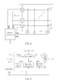
- FIG. 1 shows a block diagram of a drive system adaptable to a matrix scanning device such as, but not limited to, a touch panel or a liquid crystal display (LCD) panel, according to one embodiment of the present invention.
- a matrix scanning device such as, but not limited to, a touch panel or a liquid crystal display (LCD) panel
- the drive system includes two groups of drive circuits 11: first drive circuits (e.g., scan drive circuits) X0-Xm disposed on a first periphery along a first direction (e.g., X axis) of a substrate 10, and second drive circuits (e.g., data drive circuits) Y0-Yn disposed on a second periphery along a second direction (e.g., Y axis) of the substrate 10.
- Each drive circuit 11 is coupled to one or more column/row wires 12 of the matrix scanning device.
- the substrate 10 is the glass substrate of a touch panel as the matrix scanning device.
- the drive system also includes a master controller 13 configured to control the first drive circuits X0-Xm and the second drive circuits Y0-Yn.
- the master controller 13 is usually, but not necessarily, disposed externally to the substrate 10.
- An electrical bus 14 is electrically coupled, and configured for transferring signals, among the master controller 13, the first drive circuits X0-Xm and the second drive circuits Y0-Yn.
- One or more bus wires of the bus 14 may be configured as either analog channels (in an analog mode) or digital channels (in a digital mode).
- the bus 14 may be utilized to transfer signals, between the substrate 10 and the master controller 13, in a time-sharing and/or batch manner. Accordingly, the number of input/output pins of the master controller 13 can be substantially reduced, and the border spacer of the substrate 10 can also be reduced.
- FIG. 2 shows a detailed block diagram of one drive circuit 11 according to the embodiment of the present invention.
- the drive circuit 11 primarily includes a matrix multiplexer (matrixMUX) 110, an analog/digital multiplexer (axdMUX) 112 and a register controller 114.
- the register controller 114 is electrically coupled to the bus 14.
- the matrix multiplexer 110 is electrically coupled to at least one row/column wire 12, which is controllably communicated to one bus wire of the bus 14 via the matrix multiplexer 110, under control of the register controller 114 and an analog/digital switching signal AXD0 or AXD1 originated from the master controller 13.
- the analog/digital switching signal AXD0 is used to control the first drive circuits X0-Xm
- the analog/digital switching signal AXD1 is used to control the second drive circuits Y0-Yn.
- the matrix multiplexer 110 may be controlled by a first control signal 110A that is generated by a first logic circuit 116 under control of the register controller 114 and the analog/digital switching signal AXD0/AXD1.
- the bus 14 is switched to the analog mode; otherwise, when the analog/digital switching signal AXD0/AXD1 is "0", the bus 14 is switched to the digital mode.
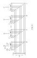
- FIG 3 shows exemplary connection of the matrix multiplexers 110 of the first drive circuits X0-Xm between the bus 14 and the column wires 12 of the matrix scanning device.
- the connection between the bus 14 and the column wire 12 is configured according to stored register content that is loaded by the master controller 13.
- the analog/digital multiplexer 112 is used to regulate the analog/digital signal transferred on the bus 14 under control of the register controller 114 and the analog/digital switching signal AXD0/AXD1.
- the analog/digital multiplexer 112 may be controlled by a second control signal 112A that is generated by a second logic circuit 118 under control of the register controller 114 and the analog/digital switching signal AXD0/AXD1.
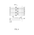
- FIG. 4 shows a detailed block diagram of the analog/digital multiplexer 112 according to the embodiment.
- a bus wire D0 is reserved to automatically figure out the total number of the configured drive circuits (e.g., X0-Xm in FIG. 1 ).
- a switch SW of its analog/digital multiplexer 112 is closed by the second control signal 112A, and a predefined signal (e.g., "0") at the bus wire node D0 is thus transferred to the bus wire node D0'.
- the last drive circuit (e.g., Xm in FIG.
- the connected drive circuits finally feed the predefined signal at its bus wire node D0' as a feedback signal FBK0 or FBK1 back to the master controller 13.
- the feedback signal FBK0 is fed back from the first drive circuit Xm
- the feedback signal FBK1 is fed back from the second drive circuit Yn.
- the master controller 13 Upon detecting the feedback signal FBK0/FBK1, the master controller 13 therefore figures out the total number of the configured drive circuits.
- some bus wires of the bus 14 may be adaptively utilized according to a specific operating mode.
- FIG. 5 shows exemplary connection among the bus 14 and the first drive circuits X0-Xm.
- the bus wires denoted spi_miso, spi_mosi and spi-clk are used as bus signals specified by Serial Peripheral Interface (SPI) standard
- SPI Serial Peripheral Interface
- the bus wires denoted samrtIO0, smartIO1 and smartIO2 are used to configure various operating modes of the drive system.
- FIG. 6 shows a timing diagram illustrated of resetting and ID-setting the drive circuits 11. Based on the ID stored in the respective register controller 114 of the drive circuit 11, each drive circuit 11 can then be addressed to perform data/ signal reading or writing.
Landscapes
- Engineering & Computer Science (AREA)
- Theoretical Computer Science (AREA)
- General Engineering & Computer Science (AREA)
- Physics & Mathematics (AREA)
- General Physics & Mathematics (AREA)
- Human Computer Interaction (AREA)
- Chemical & Material Sciences (AREA)
- Crystallography & Structural Chemistry (AREA)
- Computer Hardware Design (AREA)
- Control Of Indicators Other Than Cathode Ray Tubes (AREA)
- Position Input By Displaying (AREA)
- Electronic Switches (AREA)
- Facsimile Scanning Arrangements (AREA)
- Transforming Light Signals Into Electric Signals (AREA)
Applications Claiming Priority (1)
| Application Number | Priority Date | Filing Date | Title |
|---|---|---|---|
| CN201110127993.5A CN102789330B (zh) | 2011-05-17 | 适用于矩阵扫描装置的驱动系统 |
Publications (3)
| Publication Number | Publication Date |
|---|---|
| EP2525276A2 true EP2525276A2 (de) | 2012-11-21 |
| EP2525276A3 EP2525276A3 (de) | 2016-05-18 |
| EP2525276B1 EP2525276B1 (de) | 2020-02-05 |
Family
ID=45495652
Family Applications (1)
| Application Number | Title | Priority Date | Filing Date |
|---|---|---|---|
| EP11194175.3A Active EP2525276B1 (de) | 2011-05-17 | 2011-12-19 | An eine Matrixabtastvorrichtung anpassbares Antriebssystem |
Country Status (5)
| Country | Link |
|---|---|
| US (1) | US9423906B2 (de) |
| EP (1) | EP2525276B1 (de) |
| JP (1) | JP5670870B2 (de) |
| KR (1) | KR101406928B1 (de) |
| TW (1) | TWI467433B (de) |
Families Citing this family (3)
| Publication number | Priority date | Publication date | Assignee | Title |
|---|---|---|---|---|
| US20140184313A1 (en) * | 2012-12-27 | 2014-07-03 | Kai-Chu Chuang | Touch sensing device and a programmable controller thereof |
| FR3013472B1 (fr) | 2013-11-19 | 2016-07-08 | Fogale Nanotech | Dispositif accessoire couvrant pour un appareil portable electronique et/ou informatique, et appareil equipe d'un tel dispositif accessoire |
| US20150212609A1 (en) * | 2014-01-28 | 2015-07-30 | Apple Inc. | Light block for transparent touch sensors |
Family Cites Families (20)
| Publication number | Priority date | Publication date | Assignee | Title |
|---|---|---|---|---|
| JPS61107422A (ja) * | 1984-10-30 | 1986-05-26 | Pentel Kk | タブレツト入力装置 |
| JPH04308916A (ja) * | 1991-04-06 | 1992-10-30 | Matsushita Electric Ind Co Ltd | 位置検出装置 |
| US5893623A (en) | 1993-11-12 | 1999-04-13 | Seiko Epson Corporation | Structure and method for mounting semiconductor devices, and liquid crystal display |
| KR100202699B1 (ko) * | 1996-03-26 | 1999-06-15 | 이종수 | 아날로그/매트릭스방식 겸용 터치판넬 |
| JP3379873B2 (ja) * | 1996-04-05 | 2003-02-24 | 株式会社デジタル | マトリックス型タッチパネル入力装置 |
| JP3962969B2 (ja) * | 1998-05-29 | 2007-08-22 | オムロン株式会社 | パラレルデータ伝送方法および装置、パラレルバスシステムにおける衝突防止方法および装置 |
| JP2000259351A (ja) * | 1999-03-10 | 2000-09-22 | Keyence Corp | タッチスクリーン装置 |
| US20070233955A1 (en) * | 2000-01-06 | 2007-10-04 | Super Talent Electronics Inc. | Mixed-Mode ROM/RAM Booting Using an Integrated Flash Controller with NAND-Flash, RAM, and SD Interfaces |
| US7072825B2 (en) * | 2003-06-16 | 2006-07-04 | Fortelink, Inc. | Hierarchical, network-based emulation system |
| JP4168339B2 (ja) * | 2003-12-26 | 2008-10-22 | カシオ計算機株式会社 | 表示駆動装置及びその駆動制御方法並びに表示装置 |
| KR101288840B1 (ko) * | 2006-11-30 | 2013-07-23 | 엘지디스플레이 주식회사 | 액정표시장치 |
| US7848825B2 (en) | 2007-01-03 | 2010-12-07 | Apple Inc. | Master/slave mode for sensor processing devices |
| JP5058890B2 (ja) * | 2008-06-13 | 2012-10-24 | キヤノン株式会社 | バス制御装置 |
| JP2010108501A (ja) * | 2008-10-30 | 2010-05-13 | Samsung Electronics Co Ltd | センシング感度を向上させたタッチスクリーンコントローラ、タッチスクリーンコントローラを備えるディスプレイ駆動回路、ディスプレイ装置及びシステム |
| KR101325435B1 (ko) * | 2008-12-23 | 2013-11-08 | 엘지디스플레이 주식회사 | 액정표시장치 |
| TWI408578B (zh) * | 2009-01-22 | 2013-09-11 | Wintek Corp | 電阻式觸控裝置及其驅動方法及驅動控制器 |
| US20100225598A1 (en) * | 2009-03-05 | 2010-09-09 | Shen Jia-You | Multi-touch and handwriting-recognition resistive touchscreen |
| CN101866210B (zh) * | 2009-04-16 | 2012-03-21 | 群康科技(深圳)有限公司 | 用于电容式触控屏的省电装置及其方法与电容式触控屏 |
| US9417739B2 (en) * | 2009-05-29 | 2016-08-16 | 3M Innovative Properties Company | High speed multi-touch touch device and controller therefor |
| KR20110017315A (ko) * | 2009-08-13 | 2011-02-21 | 엘지디스플레이 주식회사 | 표시패널 구동장치 |
-
2011
- 2011-11-18 US US13/299,360 patent/US9423906B2/en active Active
- 2011-12-05 KR KR1020110128847A patent/KR101406928B1/ko active Active
- 2011-12-06 JP JP2011267101A patent/JP5670870B2/ja not_active Expired - Fee Related
- 2011-12-19 EP EP11194175.3A patent/EP2525276B1/de active Active
-
2012
- 2012-02-24 TW TW101106133A patent/TWI467433B/zh not_active IP Right Cessation
Non-Patent Citations (1)
| Title |
|---|
| None |
Also Published As
| Publication number | Publication date |
|---|---|
| JP2012243299A (ja) | 2012-12-10 |
| KR101406928B1 (ko) | 2014-06-27 |
| EP2525276A3 (de) | 2016-05-18 |
| US20120293426A1 (en) | 2012-11-22 |
| KR20120128536A (ko) | 2012-11-27 |
| CN102789330A (zh) | 2012-11-21 |
| US9423906B2 (en) | 2016-08-23 |
| TW201248467A (en) | 2012-12-01 |
| JP5670870B2 (ja) | 2015-02-18 |
| TWI467433B (zh) | 2015-01-01 |
| EP2525276B1 (de) | 2020-02-05 |
Similar Documents
| Publication | Publication Date | Title |
|---|---|---|
| US9372583B2 (en) | Display device having a touch screen and method of driving the same | |
| US9377906B2 (en) | Display device with integrated touch screen and method for driving the same | |
| JP5925279B2 (ja) | 表示装置及びその駆動方法 | |
| US9575581B2 (en) | Display device having a touch screen and method of driving the same | |
| KR101608326B1 (ko) | 터치패널 일체형 표시장치 및 그 구동 방법 | |
| US10620738B2 (en) | Touch display panel, driving method and touch display device | |
| CN109471551B (zh) | 触摸显示装置、选通驱动电路及其驱动方法 | |
| US10275077B2 (en) | Touch control display panel, touch control display device and driving method | |
| CN111916013B (zh) | 显示设备 | |
| US10055049B2 (en) | Touch sensor system and multiplexer thereof | |
| CN105159490A (zh) | 触控显示面板及其驱动方法和触控显示装置 | |
| WO2013120310A1 (zh) | 一种闸极驱动电路及驱动方法、液晶显示系统 | |
| CN105118470A (zh) | 一种栅极驱动电路及栅极驱动方法、阵列基板和显示面板 | |
| WO2021062986A1 (zh) | 触控显示面板和显示装置 | |
| US10782814B2 (en) | Touch display panel | |
| KR20130066275A (ko) | 디스플레이 드라이버 및 그것의 제조 방법 | |
| CN111752413B (zh) | 触控显示面板及其驱动方法、显示装置 | |
| CN104460065B (zh) | 液晶显示器及其测试电路 | |
| US10388243B2 (en) | Driving system and method for driving display panel and display device thereof | |
| EP2525276A2 (de) | An eine Matrixabtastvorrichtung anpassbares Antriebssystem | |
| US20210132764A1 (en) | Display device with built-in touch sensor, and drive method for same | |
| KR102416710B1 (ko) | 터치표시장치 및 그 구동방법 | |
| US20180188880A1 (en) | Touch substrate and touch display device | |
| TWI387907B (zh) | 顯示裝置及其資料讀取控制器 | |
| CN202102398U (zh) | 适用于矩阵扫描装置的驱动系统 |
Legal Events
| Date | Code | Title | Description |
|---|---|---|---|
| PUAI | Public reference made under article 153(3) epc to a published international application that has entered the european phase |
Free format text: ORIGINAL CODE: 0009012 |
|
| AK | Designated contracting states |
Kind code of ref document: A2 Designated state(s): AL AT BE BG CH CY CZ DE DK EE ES FI FR GB GR HR HU IE IS IT LI LT LU LV MC MK MT NL NO PL PT RO RS SE SI SK SM TR |
|
| AX | Request for extension of the european patent |
Extension state: BA ME |
|
| PUAL | Search report despatched |
Free format text: ORIGINAL CODE: 0009013 |
|
| RIC1 | Information provided on ipc code assigned before grant |
Ipc: G06F 3/041 20060101AFI20160407BHEP |
|
| AK | Designated contracting states |
Kind code of ref document: A3 Designated state(s): AL AT BE BG CH CY CZ DE DK EE ES FI FR GB GR HR HU IE IS IT LI LT LU LV MC MK MT NL NO PL PT RO RS SE SI SK SM TR |
|
| AX | Request for extension of the european patent |
Extension state: BA ME |
|
| 17P | Request for examination filed |
Effective date: 20160926 |
|
| RBV | Designated contracting states (corrected) |
Designated state(s): AL AT BE BG CH CY CZ DE DK EE ES FI FR GB GR HR HU IE IS IT LI LT LU LV MC MK MT NL NO PL PT RO RS SE SI SK SM TR |
|
| STAA | Information on the status of an ep patent application or granted ep patent |
Free format text: STATUS: EXAMINATION IS IN PROGRESS |
|
| 17Q | First examination report despatched |
Effective date: 20190328 |
|
| GRAP | Despatch of communication of intention to grant a patent |
Free format text: ORIGINAL CODE: EPIDOSNIGR1 |
|
| STAA | Information on the status of an ep patent application or granted ep patent |
Free format text: STATUS: GRANT OF PATENT IS INTENDED |
|
| RIC1 | Information provided on ipc code assigned before grant |
Ipc: G06F 3/047 20060101ALI20190731BHEP Ipc: G06F 3/041 20060101AFI20190731BHEP Ipc: G06F 3/044 20060101ALI20190731BHEP |
|
| INTG | Intention to grant announced |
Effective date: 20190904 |
|
| GRAS | Grant fee paid |
Free format text: ORIGINAL CODE: EPIDOSNIGR3 |
|
| GRAA | (expected) grant |
Free format text: ORIGINAL CODE: 0009210 |
|
| STAA | Information on the status of an ep patent application or granted ep patent |
Free format text: STATUS: THE PATENT HAS BEEN GRANTED |
|
| AK | Designated contracting states |
Kind code of ref document: B1 Designated state(s): AL AT BE BG CH CY CZ DE DK EE ES FI FR GB GR HR HU IE IS IT LI LT LU LV MC MK MT NL NO PL PT RO RS SE SI SK SM TR |
|
| REG | Reference to a national code |
Ref country code: GB Ref legal event code: FG4D |
|
| REG | Reference to a national code |
Ref country code: AT Ref legal event code: REF Ref document number: 1230355 Country of ref document: AT Kind code of ref document: T Effective date: 20200215 |
|
| REG | Reference to a national code |
Ref country code: DE Ref legal event code: R096 Ref document number: 602011064829 Country of ref document: DE |
|
| REG | Reference to a national code |
Ref country code: IE Ref legal event code: FG4D |
|
| REG | Reference to a national code |
Ref country code: CH Ref legal event code: EP |
|
| REG | Reference to a national code |
Ref country code: NL Ref legal event code: MP Effective date: 20200205 |
|
| PG25 | Lapsed in a contracting state [announced via postgrant information from national office to epo] |
Ref country code: NO Free format text: LAPSE BECAUSE OF FAILURE TO SUBMIT A TRANSLATION OF THE DESCRIPTION OR TO PAY THE FEE WITHIN THE PRESCRIBED TIME-LIMIT Effective date: 20200505 Ref country code: FI Free format text: LAPSE BECAUSE OF FAILURE TO SUBMIT A TRANSLATION OF THE DESCRIPTION OR TO PAY THE FEE WITHIN THE PRESCRIBED TIME-LIMIT Effective date: 20200205 Ref country code: PT Free format text: LAPSE BECAUSE OF FAILURE TO SUBMIT A TRANSLATION OF THE DESCRIPTION OR TO PAY THE FEE WITHIN THE PRESCRIBED TIME-LIMIT Effective date: 20200628 Ref country code: RS Free format text: LAPSE BECAUSE OF FAILURE TO SUBMIT A TRANSLATION OF THE DESCRIPTION OR TO PAY THE FEE WITHIN THE PRESCRIBED TIME-LIMIT Effective date: 20200205 |
|
| REG | Reference to a national code |
Ref country code: LT Ref legal event code: MG4D |
|
| PG25 | Lapsed in a contracting state [announced via postgrant information from national office to epo] |
Ref country code: IS Free format text: LAPSE BECAUSE OF FAILURE TO SUBMIT A TRANSLATION OF THE DESCRIPTION OR TO PAY THE FEE WITHIN THE PRESCRIBED TIME-LIMIT Effective date: 20200605 Ref country code: LV Free format text: LAPSE BECAUSE OF FAILURE TO SUBMIT A TRANSLATION OF THE DESCRIPTION OR TO PAY THE FEE WITHIN THE PRESCRIBED TIME-LIMIT Effective date: 20200205 Ref country code: SE Free format text: LAPSE BECAUSE OF FAILURE TO SUBMIT A TRANSLATION OF THE DESCRIPTION OR TO PAY THE FEE WITHIN THE PRESCRIBED TIME-LIMIT Effective date: 20200205 Ref country code: GR Free format text: LAPSE BECAUSE OF FAILURE TO SUBMIT A TRANSLATION OF THE DESCRIPTION OR TO PAY THE FEE WITHIN THE PRESCRIBED TIME-LIMIT Effective date: 20200506 Ref country code: BG Free format text: LAPSE BECAUSE OF FAILURE TO SUBMIT A TRANSLATION OF THE DESCRIPTION OR TO PAY THE FEE WITHIN THE PRESCRIBED TIME-LIMIT Effective date: 20200505 Ref country code: HR Free format text: LAPSE BECAUSE OF FAILURE TO SUBMIT A TRANSLATION OF THE DESCRIPTION OR TO PAY THE FEE WITHIN THE PRESCRIBED TIME-LIMIT Effective date: 20200205 |
|
| PG25 | Lapsed in a contracting state [announced via postgrant information from national office to epo] |
Ref country code: NL Free format text: LAPSE BECAUSE OF FAILURE TO SUBMIT A TRANSLATION OF THE DESCRIPTION OR TO PAY THE FEE WITHIN THE PRESCRIBED TIME-LIMIT Effective date: 20200205 |
|
| PG25 | Lapsed in a contracting state [announced via postgrant information from national office to epo] |
Ref country code: ES Free format text: LAPSE BECAUSE OF FAILURE TO SUBMIT A TRANSLATION OF THE DESCRIPTION OR TO PAY THE FEE WITHIN THE PRESCRIBED TIME-LIMIT Effective date: 20200205 Ref country code: RO Free format text: LAPSE BECAUSE OF FAILURE TO SUBMIT A TRANSLATION OF THE DESCRIPTION OR TO PAY THE FEE WITHIN THE PRESCRIBED TIME-LIMIT Effective date: 20200205 Ref country code: SK Free format text: LAPSE BECAUSE OF FAILURE TO SUBMIT A TRANSLATION OF THE DESCRIPTION OR TO PAY THE FEE WITHIN THE PRESCRIBED TIME-LIMIT Effective date: 20200205 Ref country code: CZ Free format text: LAPSE BECAUSE OF FAILURE TO SUBMIT A TRANSLATION OF THE DESCRIPTION OR TO PAY THE FEE WITHIN THE PRESCRIBED TIME-LIMIT Effective date: 20200205 Ref country code: SM Free format text: LAPSE BECAUSE OF FAILURE TO SUBMIT A TRANSLATION OF THE DESCRIPTION OR TO PAY THE FEE WITHIN THE PRESCRIBED TIME-LIMIT Effective date: 20200205 Ref country code: EE Free format text: LAPSE BECAUSE OF FAILURE TO SUBMIT A TRANSLATION OF THE DESCRIPTION OR TO PAY THE FEE WITHIN THE PRESCRIBED TIME-LIMIT Effective date: 20200205 Ref country code: LT Free format text: LAPSE BECAUSE OF FAILURE TO SUBMIT A TRANSLATION OF THE DESCRIPTION OR TO PAY THE FEE WITHIN THE PRESCRIBED TIME-LIMIT Effective date: 20200205 Ref country code: DK Free format text: LAPSE BECAUSE OF FAILURE TO SUBMIT A TRANSLATION OF THE DESCRIPTION OR TO PAY THE FEE WITHIN THE PRESCRIBED TIME-LIMIT Effective date: 20200205 |
|
| REG | Reference to a national code |
Ref country code: DE Ref legal event code: R097 Ref document number: 602011064829 Country of ref document: DE |
|
| REG | Reference to a national code |
Ref country code: AT Ref legal event code: MK05 Ref document number: 1230355 Country of ref document: AT Kind code of ref document: T Effective date: 20200205 |
|
| PLBE | No opposition filed within time limit |
Free format text: ORIGINAL CODE: 0009261 |
|
| STAA | Information on the status of an ep patent application or granted ep patent |
Free format text: STATUS: NO OPPOSITION FILED WITHIN TIME LIMIT |
|
| 26N | No opposition filed |
Effective date: 20201106 |
|
| PG25 | Lapsed in a contracting state [announced via postgrant information from national office to epo] |
Ref country code: AT Free format text: LAPSE BECAUSE OF FAILURE TO SUBMIT A TRANSLATION OF THE DESCRIPTION OR TO PAY THE FEE WITHIN THE PRESCRIBED TIME-LIMIT Effective date: 20200205 Ref country code: IT Free format text: LAPSE BECAUSE OF FAILURE TO SUBMIT A TRANSLATION OF THE DESCRIPTION OR TO PAY THE FEE WITHIN THE PRESCRIBED TIME-LIMIT Effective date: 20200205 |
|
| PG25 | Lapsed in a contracting state [announced via postgrant information from national office to epo] |
Ref country code: PL Free format text: LAPSE BECAUSE OF FAILURE TO SUBMIT A TRANSLATION OF THE DESCRIPTION OR TO PAY THE FEE WITHIN THE PRESCRIBED TIME-LIMIT Effective date: 20200205 Ref country code: SI Free format text: LAPSE BECAUSE OF FAILURE TO SUBMIT A TRANSLATION OF THE DESCRIPTION OR TO PAY THE FEE WITHIN THE PRESCRIBED TIME-LIMIT Effective date: 20200205 |
|
| REG | Reference to a national code |
Ref country code: CH Ref legal event code: PL |
|
| GBPC | Gb: european patent ceased through non-payment of renewal fee |
Effective date: 20201219 |
|
| PG25 | Lapsed in a contracting state [announced via postgrant information from national office to epo] |
Ref country code: MC Free format text: LAPSE BECAUSE OF FAILURE TO SUBMIT A TRANSLATION OF THE DESCRIPTION OR TO PAY THE FEE WITHIN THE PRESCRIBED TIME-LIMIT Effective date: 20200205 |
|
| REG | Reference to a national code |
Ref country code: BE Ref legal event code: MM Effective date: 20201231 |
|
| PG25 | Lapsed in a contracting state [announced via postgrant information from national office to epo] |
Ref country code: LU Free format text: LAPSE BECAUSE OF NON-PAYMENT OF DUE FEES Effective date: 20201219 Ref country code: IE Free format text: LAPSE BECAUSE OF NON-PAYMENT OF DUE FEES Effective date: 20201219 |
|
| PG25 | Lapsed in a contracting state [announced via postgrant information from national office to epo] |
Ref country code: GB Free format text: LAPSE BECAUSE OF NON-PAYMENT OF DUE FEES Effective date: 20201219 Ref country code: CH Free format text: LAPSE BECAUSE OF NON-PAYMENT OF DUE FEES Effective date: 20201231 Ref country code: LI Free format text: LAPSE BECAUSE OF NON-PAYMENT OF DUE FEES Effective date: 20201231 |
|
| PG25 | Lapsed in a contracting state [announced via postgrant information from national office to epo] |
Ref country code: TR Free format text: LAPSE BECAUSE OF FAILURE TO SUBMIT A TRANSLATION OF THE DESCRIPTION OR TO PAY THE FEE WITHIN THE PRESCRIBED TIME-LIMIT Effective date: 20200205 Ref country code: MT Free format text: LAPSE BECAUSE OF FAILURE TO SUBMIT A TRANSLATION OF THE DESCRIPTION OR TO PAY THE FEE WITHIN THE PRESCRIBED TIME-LIMIT Effective date: 20200205 Ref country code: CY Free format text: LAPSE BECAUSE OF FAILURE TO SUBMIT A TRANSLATION OF THE DESCRIPTION OR TO PAY THE FEE WITHIN THE PRESCRIBED TIME-LIMIT Effective date: 20200205 |
|
| PG25 | Lapsed in a contracting state [announced via postgrant information from national office to epo] |
Ref country code: MK Free format text: LAPSE BECAUSE OF FAILURE TO SUBMIT A TRANSLATION OF THE DESCRIPTION OR TO PAY THE FEE WITHIN THE PRESCRIBED TIME-LIMIT Effective date: 20200205 Ref country code: AL Free format text: LAPSE BECAUSE OF FAILURE TO SUBMIT A TRANSLATION OF THE DESCRIPTION OR TO PAY THE FEE WITHIN THE PRESCRIBED TIME-LIMIT Effective date: 20200205 |
|
| PG25 | Lapsed in a contracting state [announced via postgrant information from national office to epo] |
Ref country code: BE Free format text: LAPSE BECAUSE OF NON-PAYMENT OF DUE FEES Effective date: 20201231 |
|
| PGFP | Annual fee paid to national office [announced via postgrant information from national office to epo] |
Ref country code: FR Payment date: 20231009 Year of fee payment: 13 Ref country code: DE Payment date: 20231024 Year of fee payment: 13 |
|
| REG | Reference to a national code |
Ref country code: DE Ref legal event code: R119 Ref document number: 602011064829 Country of ref document: DE |
|
| PG25 | Lapsed in a contracting state [announced via postgrant information from national office to epo] |
Ref country code: DE Free format text: LAPSE BECAUSE OF NON-PAYMENT OF DUE FEES Effective date: 20250701 |
|
| PG25 | Lapsed in a contracting state [announced via postgrant information from national office to epo] |
Ref country code: FR Free format text: LAPSE BECAUSE OF NON-PAYMENT OF DUE FEES Effective date: 20241231 |