EP2519087A1 - Einkapselungshülle für ein System mit elektrischen Verbindungen, Herstellungsverfahren dergleichen, mit einer solchen Hülle versehenes eingekapseltes System und Stapeln solcher Systeme - Google Patents
Einkapselungshülle für ein System mit elektrischen Verbindungen, Herstellungsverfahren dergleichen, mit einer solchen Hülle versehenes eingekapseltes System und Stapeln solcher Systeme Download PDFInfo
- Publication number
- EP2519087A1 EP2519087A1 EP12165906A EP12165906A EP2519087A1 EP 2519087 A1 EP2519087 A1 EP 2519087A1 EP 12165906 A EP12165906 A EP 12165906A EP 12165906 A EP12165906 A EP 12165906A EP 2519087 A1 EP2519087 A1 EP 2519087A1
- Authority
- EP
- European Patent Office
- Prior art keywords
- hole
- cover
- conductive material
- electrical contact
- hood
- Prior art date
- Legal status (The legal status is an assumption and is not a legal conclusion. Google has not performed a legal analysis and makes no representation as to the accuracy of the status listed.)
- Granted
Links
Images


Classifications
-
- H—ELECTRICITY
- H05—ELECTRIC TECHNIQUES NOT OTHERWISE PROVIDED FOR
- H05K—PRINTED CIRCUITS; CASINGS OR CONSTRUCTIONAL DETAILS OF ELECTRIC APPARATUS; MANUFACTURE OF ASSEMBLAGES OF ELECTRICAL COMPONENTS
- H05K1/00—Printed circuits
- H05K1/02—Details
- H05K1/11—Printed elements for providing electric connections to or between printed circuits
- H05K1/115—Via connections; Lands around holes or via connections
-
- H—ELECTRICITY
- H05—ELECTRIC TECHNIQUES NOT OTHERWISE PROVIDED FOR
- H05K—PRINTED CIRCUITS; CASINGS OR CONSTRUCTIONAL DETAILS OF ELECTRIC APPARATUS; MANUFACTURE OF ASSEMBLAGES OF ELECTRICAL COMPONENTS
- H05K3/00—Apparatus or processes for manufacturing printed circuits
- H05K3/40—Forming printed elements for providing electric connections to or between printed circuits
- H05K3/42—Plated through-holes or plated via connections
-
- H—ELECTRICITY
- H05—ELECTRIC TECHNIQUES NOT OTHERWISE PROVIDED FOR
- H05K—PRINTED CIRCUITS; CASINGS OR CONSTRUCTIONAL DETAILS OF ELECTRIC APPARATUS; MANUFACTURE OF ASSEMBLAGES OF ELECTRICAL COMPONENTS
- H05K2201/00—Indexing scheme relating to printed circuits covered by H05K1/00
- H05K2201/04—Assemblies of printed circuits
- H05K2201/041—Stacked PCBs, i.e. having neither an empty space nor mounted components in between
-
- H—ELECTRICITY
- H05—ELECTRIC TECHNIQUES NOT OTHERWISE PROVIDED FOR
- H05K—PRINTED CIRCUITS; CASINGS OR CONSTRUCTIONAL DETAILS OF ELECTRIC APPARATUS; MANUFACTURE OF ASSEMBLAGES OF ELECTRICAL COMPONENTS
- H05K2201/00—Indexing scheme relating to printed circuits covered by H05K1/00
- H05K2201/06—Thermal details
- H05K2201/068—Thermal details wherein the coefficient of thermal expansion is important
-
- H—ELECTRICITY
- H05—ELECTRIC TECHNIQUES NOT OTHERWISE PROVIDED FOR
- H05K—PRINTED CIRCUITS; CASINGS OR CONSTRUCTIONAL DETAILS OF ELECTRIC APPARATUS; MANUFACTURE OF ASSEMBLAGES OF ELECTRICAL COMPONENTS
- H05K2201/00—Indexing scheme relating to printed circuits covered by H05K1/00
- H05K2201/09—Shape and layout
- H05K2201/09209—Shape and layout details of conductors
- H05K2201/095—Conductive through-holes or vias
- H05K2201/09563—Metal filled via
-
- H—ELECTRICITY
- H05—ELECTRIC TECHNIQUES NOT OTHERWISE PROVIDED FOR
- H05K—PRINTED CIRCUITS; CASINGS OR CONSTRUCTIONAL DETAILS OF ELECTRIC APPARATUS; MANUFACTURE OF ASSEMBLAGES OF ELECTRICAL COMPONENTS
- H05K2201/00—Indexing scheme relating to printed circuits covered by H05K1/00
- H05K2201/09—Shape and layout
- H05K2201/09818—Shape or layout details not covered by a single group of H05K2201/09009 - H05K2201/09809
- H05K2201/09827—Tapered, e.g. tapered hole, via or groove
-
- H—ELECTRICITY
- H05—ELECTRIC TECHNIQUES NOT OTHERWISE PROVIDED FOR
- H05K—PRINTED CIRCUITS; CASINGS OR CONSTRUCTIONAL DETAILS OF ELECTRIC APPARATUS; MANUFACTURE OF ASSEMBLAGES OF ELECTRICAL COMPONENTS
- H05K2201/00—Indexing scheme relating to printed circuits covered by H05K1/00
- H05K2201/09—Shape and layout
- H05K2201/09818—Shape or layout details not covered by a single group of H05K2201/09009 - H05K2201/09809
- H05K2201/09854—Hole or via having special cross-section, e.g. elliptical
-
- H—ELECTRICITY
- H05—ELECTRIC TECHNIQUES NOT OTHERWISE PROVIDED FOR
- H05K—PRINTED CIRCUITS; CASINGS OR CONSTRUCTIONAL DETAILS OF ELECTRIC APPARATUS; MANUFACTURE OF ASSEMBLAGES OF ELECTRICAL COMPONENTS
- H05K2201/00—Indexing scheme relating to printed circuits covered by H05K1/00
- H05K2201/10—Details of components or other objects attached to or integrated in a printed circuit board
- H05K2201/10227—Other objects, e.g. metallic pieces
- H05K2201/10378—Interposers
-
- H—ELECTRICITY
- H05—ELECTRIC TECHNIQUES NOT OTHERWISE PROVIDED FOR
- H05K—PRINTED CIRCUITS; CASINGS OR CONSTRUCTIONAL DETAILS OF ELECTRIC APPARATUS; MANUFACTURE OF ASSEMBLAGES OF ELECTRICAL COMPONENTS
- H05K2203/00—Indexing scheme relating to apparatus or processes for manufacturing printed circuits covered by H05K3/00
- H05K2203/02—Details related to mechanical or acoustic processing, e.g. drilling, punching, cutting, using ultrasound
- H05K2203/025—Abrading, e.g. grinding or sand blasting
-
- H—ELECTRICITY
- H05—ELECTRIC TECHNIQUES NOT OTHERWISE PROVIDED FOR
- H05K—PRINTED CIRCUITS; CASINGS OR CONSTRUCTIONAL DETAILS OF ELECTRIC APPARATUS; MANUFACTURE OF ASSEMBLAGES OF ELECTRICAL COMPONENTS
- H05K2203/00—Indexing scheme relating to apparatus or processes for manufacturing printed circuits covered by H05K3/00
- H05K2203/15—Position of the PCB during processing
- H05K2203/1572—Processing both sides of a PCB by the same process; Providing a similar arrangement of components on both sides; Making interlayer connections from two sides
-
- H—ELECTRICITY
- H05—ELECTRIC TECHNIQUES NOT OTHERWISE PROVIDED FOR
- H05K—PRINTED CIRCUITS; CASINGS OR CONSTRUCTIONAL DETAILS OF ELECTRIC APPARATUS; MANUFACTURE OF ASSEMBLAGES OF ELECTRICAL COMPONENTS
- H05K3/00—Apparatus or processes for manufacturing printed circuits
- H05K3/0011—Working of insulating substrates or insulating layers
- H05K3/0017—Etching of the substrate by chemical or physical means
-
- H—ELECTRICITY
- H05—ELECTRIC TECHNIQUES NOT OTHERWISE PROVIDED FOR
- H05K—PRINTED CIRCUITS; CASINGS OR CONSTRUCTIONAL DETAILS OF ELECTRIC APPARATUS; MANUFACTURE OF ASSEMBLAGES OF ELECTRICAL COMPONENTS
- H05K3/00—Apparatus or processes for manufacturing printed circuits
- H05K3/40—Forming printed elements for providing electric connections to or between printed circuits
- H05K3/4038—Through-connections; Vertical interconnect access [VIA] connections
- H05K3/4053—Through-connections; Vertical interconnect access [VIA] connections by thick-film techniques
- H05K3/4061—Through-connections; Vertical interconnect access [VIA] connections by thick-film techniques for via connections in inorganic insulating substrates
Definitions
- the present invention relates to a cover having electrical contacts between its two faces and which is intended for the hermetic encapsulation of systems or microsystems requiring electrical connections.
- the present invention relates to a cover comprising a front face and a rear face and at least one through hole connecting said front face to said rear face and intended to receive an electrical contact.
- the invention also relates to a cover provided with at least one electrical contact, a system or microsystem encapsulated by means of such a cover and a method of manufacturing such a cover.
- TSV Through-Silicon Vias when the cover is silicon
- TGV Through-Glass Vias
- This cover will then be assembled on the substrate comprising the microsystem, revealing both two assembly or bonding zones.
- the assembly can be achieved by various techniques, such as welding, thermocompression, anodic bonding or cottage.
- these contacts allow the formation of complex systems of stacking and interconnection of different chips. These contacts are also very useful for the encapsulation under controlled atmosphere of MEMS.
- these contacts are made by drilling a hole through the hood.
- the cover is silicon for example
- the walls of the through hole are then covered with an insulating layer.
- the through hole is then filled with metal, either in the form of metal paste or by a galvanic process involving a deposit from a metal base assembled on the cover or via a first metal layer deposited by evaporation.
- these through holes have a straight profile, as described in the patent application US 2004/264152 , or slightly conical, as described in the WO 2004/095573 or US 2010/096712 . It is necessary to provide an overgrowth or protrusion of metal to ensure the mechanical stability of the contact thus formed, in the manner of a rivet, as described in the publication IMEC, Scientific Report 2008, 3D wafer level packaging (3D-WLP) or in the application US 2011/012248 .
- Such protuberances may be provided on one or other of the faces of the cover, or on both sides.
- the rivet shape induces extra thicknesses on the surface of the cover, which can be disadvantageous for the assembly steps, especially for thermocompression which requires a flat topology and a very low roughness , as well as for subsequent steps of manufacturing a hood surface system, or else of making flexible micro-elements of contact by a manufacturing based on microphotolithography, for which a spring for example is added to the surface of the electrical contact.
- thermocompression assembly a mechanical force is applied to the contact, may weaken or move, which will induce a faulty contact but especially a loss of sealing.
- This contact must therefore have excellent mechanical stability irrespective of the direction of the applied force.
- a subsequent assembly can be performed for the manufacture of a sensor assembly or stack or for mounting on an interface substrate, of the PCB type, for example.
- this system may have large pressure differences (gas or liquid) between the outside and the inside of the hermetic cavity formed between the substrate and the cover.
- An object of the present invention is to provide an encapsulation cover of a system with electrical connections, said cover comprising through electrical contacts which are insensitive to thermal effects and mechanically stable to allow assembly by thermocompression.
- Another object of the present invention is to provide a cover comprising through electrical contacts having a shape allowing assembly by optimum stacking of different systems.
- a hermetic encapsulation cover of a system or microsystem with electrical connections comprising a front face and a rear face and at at least one through hole connecting said front face to said rear face and for receiving an electrical contact.
- said through hole has at least one convergent portion and at least one divergent portion connected by a connecting collar.
- the electrical contact created by filling such a through hole is mechanically stable without it being necessary to provide protuberances on the surface of the cover.
- the electrical contact thus has no part out of the plane of the two sides of the cover, allowing optimum stacking of several systems.
- the present invention also relates to a method of manufacturing a hood as defined above, said method comprising a step of forming in the bonnet of a through hole connecting the front face to the rear face and intended to receive an electrical contact.
- said through hole having at least one converging portion and at least one diverging portion connected by a connecting neck.
- the present invention also relates to a method of manufacturing a cover as defined above and comprising, disposed in its through hole, an electrical contact made in at least one conductive material, said method comprising a forming step in the cover of a through hole connecting the front face to the rear face and intended to receive an electrical contact, said through hole having at least one convergent portion and at least one divergent portion connected by a junction neck, and a step of depositing said material conductive in the through hole.
- the present invention also relates to an encapsulated system or microsystems requiring electrical connections, comprising at least one substrate hermetically assembled to at least one cover as defined above and comprising, disposed in at least one through hole, at least one contact electric, and electrical connection means between said system and the electrical contact.
- the present invention also relates to a stack of encapsulated systems or microsystems requiring electrical connections, comprising at least two substrates assembled respectively, so as to hermetic, at least one cover as defined above and comprising, disposed in at least one through hole, at least one electrical contact, and electrical connection means between each of said systems and the electrical contact.
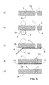
- the cover 2 comprises a front face 2a and a rear face 2b and at least one through hole 1 connecting said front face 2a to said rear face 2b and intended to receive an electrical contact 6.
- the inner face of the cover may be flat or have an inner shape adapted to receive a microsystem.
- said through hole 1 has a converging portion 3 and a diverging portion 5 connected by a connecting collar 4.
- the convergent portion 3 converges from the front face 2a of the cover 2 to said connecting collar 4 and the diverging portion 5 diverges from the joining collar 4 to the rear face 2b of the cover 2.
- said through hole 1 comprises converging or diverging walls which, in axial section, have a straight shape.
- the through hole 1 is in the form of two cone-shaped truncated cones connected by the joining neck 4.
- the through hole may comprise converging or diverging walls which, in axial section, have a curved shape, so that the through hole has a diabolo shape.
- the cross section of the through hole can be of any shape, such as round, square, or rectangular.
- the connecting collar 4 is, relative to each of the front faces 2a and 2b of the rear cover 2, at a distance corresponding to at least 10%, preferably at least 15%, of the thickness of the cover 2 .
- the convergent part 3, respectively the diverging portion 5, is advantageously made so that its opening angle ⁇ with respect to the plane of the front face 2a, respectively rear 2b, of the cover 2 is between 60 ° and 85 °. °, and preferably between 68 ° and 78 °.
- the cover 2 may be a plate made of glass, ceramic, polymer (pure or composite) or semiconductor material, such as silicon.
- the cover 2 may have a thickness of between 50 microns and 2 mm, and preferably between 150 microns and 1 mm.
- the dimensions of the convergent 3 and divergent portions 5 are preferably such that the dimensions of the opening of the through-hole taken on the surface of the cap 2 are between 10 ⁇ m and 500 ⁇ m, and preferably between 100 ⁇ m and 300 ⁇ m.
- the connecting collar 4 has an opening whose size is less than 80% of the dimension of the smallest opening of the through hole, taken on the surface of the front face 2a or the rear face 2b of the cover 2.
- the size of the opening of the connecting collar is however sufficient to allow the filling of the through hole by the conductive material to form the electrical contact.
- the through hole 1 has only one joining neck 4 so that all the covers having through holes formed by annealing and having roughness are not part of the invention.
- the electrical contact 6 disposed in the through hole 1 formed according to the invention in the cover 2 is made of at least one conductive material which may comprise at least one metal or at least one metal alloy, such as copper, gold or any other suitable metal or metal alloy.
- the conductive material comprises a first conductive material at least partially constituting said electrical contact 6.
- said first conductive material has a coefficient of thermal expansion having a difference of at most 3 ppm relative to that of the cover 2.
- said first conductive material is an alloy of iron and nickel, in which the mass content of nickel is between 20% and 80%, preferably between 25% and 50%, and more preferably between 32%. and 40% of the alloy.
- the conductive material of said electrical contact may comprise at least one second conductive material.
- Said at least second conductive material may be in the form of layers, for example alternating with layers of the first conductive material, or may form with said first conductive material a heterogeneous assembly.
- the second material may for example be provided in the form of a layer on the surface of the electrical contact.
- the second conductive material may be gold or any other suitable metal or metal alloy.
- the electrical contact 6 created by filling said through hole 1, is stable mechanically. It is therefore insensitive to vertical thrusts that could be applied. As a result, the electrical contact 6 does not require any parts protruding from the faces of the cover 2. Thus, the electrical contact 6 has plane free surfaces that respectively project from the front face 2a and the rear face 2b of the cover 2. .
- the hood 2 according to the invention comprises a flexible element 20 provided on the flat surface of the electrical contact 6.
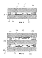
- the figure 5 represents an encapsulated system comprising a substrate 22 sealed to a hood 2 according to the invention.
- a system or microsystem 24 such as a MEMS.
- the electrical connection between the contact 6 of the cover 2 and the microsystem 24 is achieved by means of an interface weld 26.
- the sealing of the assembly is carried out by means of a weld bead 28.
- Such a system can for example, electronic components or microsensors that must be encapsulated to place the sensing element in a controlled atmosphere. Thus it can reign a pressure P1 inside the cavity, different from the external pressure P0.
- the specific form of the through contact 6 according to the invention allows the latter to remain in place and preserve the tightness of the system, even in case of very large pressure difference between the inside of the cavity 23 and the outside of the system.
- Another advantage of the shape of the through contact is that during assembly of the cover 2 and the substrate 22, the inner surface of the contact 6 is at the same height as the weld bead 28, which facilitates assembly by thermocompression .
- FIG 6 shows an exemplary embodiment of such a stack, comprising two microsystems 24a, 24b, for example of the MEMS type, each provided on a substrate 22a, 22b respectively, and connected by a cover 2 according to the invention.
- Said hood 2 allows, with the weld seams 28a, 28b to encapsulate the systems 24a, 24b.
- the electrical connections between the microsystems 24a, 24b are made by means of interfacing welds 26a, 26b connecting the electrical contact 6 to the microsystem 24a, 24b, respectively.
- it can be a pressure P1 inside the first cavity 23a, a pressure P2 inside the second cavity 23b, different from each other, and also different from the external pressure P0.
- the temperature resistance of the electrical contact 6 according to the invention is much better than the riveted and straight-walled contacts. Indeed, during a greater expansion of the metal constituting the electrical contact that the hood material, the forces exerted laterally are much lower because the inclination of the walls of the hole breaks down this bearing force into a lateral component and a vertical component.
- the present invention also relates to a method of manufacturing a hood as described above, comprising a forming step in the cover 2 of a through hole 1 connecting the front face 2a to the rear face 2b of the cover 2, said through hole 1 having at least one converging portion 3 and at least one diverging portion 5 connected by a connecting collar 4.
- the through hole is formed by an etching process through a mask.
- the shape of the through hole according to the invention can be obtained by using, from each face of the cover, an etching process, for example anisotropic, through a mask, such as a wet etching, a plasma etching or an engraving by sandblasting.
- the method according to the invention comprises a step of depositing, in the through hole, the conductive material in which the electrical contact is made.
- the conductive material completely fills the through hole so that the free surfaces of the electrical contact respectively flush with the front face 2a and the rear face 2b of the cover 2.
- the conductive material may be deposited galvanically or in the form of a paste stabilized by heating after its introduction into the through hole.
- the walls of the hole must be covered with an electrical insulator, for example by forming a thermal oxide in the case of silicon.
- the method according to the invention may comprise, between the step of forming the through hole and the step of depositing the conductive material, a step of positioning a conductive sheet on one of the front and rear faces of the cover.
- the method according to the invention may comprise, prior to the step of positioning said conductive sheet, a step of depositing, on one of the front and rear faces of the cover, an adhesive material having a controlled viscosity so as to do not enter the through hole.
- the method according to the invention may comprise, prior to the step of positioning said conductive sheet, a step of depositing, on one of the front and rear faces of the cover, an adhesive material having a opening at the through hole.
- said adhesive material may be selectively deposited on one of the faces so as not to block the contact holes, for example by an ink jet printing method, or it may be deposited on any face. in the form of a glue film, and then selectively open to clear the holes.
- the method according to the invention further comprises a finishing step comprising a mechanical treatment of the surface of the cover, to obtain a cover comprising planar and polished through electrical contacts.
- step a) the cover 2, here chosen initially insulating, is pierced with a through hole 1 having the profile according to the invention, by means of an attack on each face of the cover 2 by sandblasting through resin masks.
- step b) after removal of the masks, a layer of adhesive material 8, for example an adhesive, is applied by means of a dispensing system identical to those of the inking systems used in printing.
- a layer of glue of controlled thickness 9 is deposited only on the rear face 2b of the cover 2 which has been in contact with the applicator roll 7.
- the viscosity of the glue is chosen so that it does not not flow into the through hole 1.
- step c) a sheet of metal 11, for example made of brass, is then applied to the rear face 2b of the cover 2 by pressing on the adhesive layer 9 by means of rolling rolls 10.
- the unglued face of the metal sheet 11 may be covered with an electrical insulator (not shown).
- step d) the bottom of the through hole 1 then consists of the conductive surface of the metal sheet 11 from which a galvanic deposition of a metal or a metal alloy makes it possible to make an electrical contact 12 at through the hood 2.
- step e) a lapping and polishing on the two front faces 2a and 2b of the rear cover 2 then make it possible to obtain a plane and polished cap, with an electrical contact 6 through and sealed.
- the metal sheet 11 may, however, be retained at least partially to allow engraving tracks to achieve interconnections.
- the present invention also relates to a cover comprising a front face and a rear face, at least one through hole connecting said front face to said rear face, and an electrical contact disposed in said through hole and made of a conducting material consisting at least partially of a conductive material.
- Said conducting material is an alloy of iron and nickel, in which the mass content of nickel is between 20% and 80%, preferably between 25% and 50%, and more preferably between 32% and 40% of the alloy. .
- Such an alloy makes it possible to adjust the coefficient of thermal expansion of the material constituting the contact so that it has a difference of at most 3 ppm with respect to that of the cover.
- the iron / nickel alloy for filling all or part of the through hole for form all or part of the electrical contact.
- the through hole can be of any shape.
Landscapes
- Engineering & Computer Science (AREA)
- Microelectronics & Electronic Packaging (AREA)
- Manufacturing & Machinery (AREA)
- Printing Elements For Providing Electric Connections Between Printed Circuits (AREA)
- Manufacturing Of Electrical Connectors (AREA)
- Micromachines (AREA)
Applications Claiming Priority (1)
| Application Number | Priority Date | Filing Date | Title |
|---|---|---|---|
| CH00738/11A CH704884B1 (fr) | 2011-04-29 | 2011-04-29 | Substrat destiné à recevoir des contacts électriques. |
Publications (2)
| Publication Number | Publication Date |
|---|---|
| EP2519087A1 true EP2519087A1 (de) | 2012-10-31 |
| EP2519087B1 EP2519087B1 (de) | 2018-12-26 |
Family
ID=44487122
Family Applications (1)
| Application Number | Title | Priority Date | Filing Date |
|---|---|---|---|
| EP12165906.4A Not-in-force EP2519087B1 (de) | 2011-04-29 | 2012-04-27 | Einkapselungshülle für ein System mit elektrischen Verbindungen, Herstellungsverfahren dergleichen, mit einer solchen Hülle versehenes eingekapseltes System und Stapeln solcher Systeme |
Country Status (2)
| Country | Link |
|---|---|
| EP (1) | EP2519087B1 (de) |
| CH (1) | CH704884B1 (de) |
Citations (15)
| Publication number | Priority date | Publication date | Assignee | Title |
|---|---|---|---|---|
| US5610431A (en) * | 1995-05-12 | 1997-03-11 | The Charles Stark Draper Laboratory, Inc. | Covers for micromechanical sensors and other semiconductor devices |
| US20010027842A1 (en) * | 1999-08-26 | 2001-10-11 | International Business Machines Corporation | Method for filling high aspect ratio via holes in electronic substrates and the resulting holes |
| US6331678B1 (en) * | 1999-10-29 | 2001-12-18 | Agilent Technologies, Inc. | Reduction of blistering and delamination of high-temperature devices with metal film |
| US20020180015A1 (en) * | 2001-05-31 | 2002-12-05 | Yoshihide Yamaguchi | Semiconductor module |
| WO2004095573A1 (en) | 2003-03-26 | 2004-11-04 | Northrop Grumman Corporation | Wafer scale package and method of assembly |
| GB2401485A (en) * | 2002-12-11 | 2004-11-10 | Dainippon Printing Co Ltd | Multilayer printed circuit board and method for manufacturing same |
| US20040264152A1 (en) | 2003-06-25 | 2004-12-30 | Heck John M. | MEMS RF switch module including a vertical via |
| US20060021794A1 (en) * | 2004-07-27 | 2006-02-02 | Cheng David C H | Process of fabricating conductive column and circuit board with conductive column |
| WO2007003228A1 (de) * | 2005-06-30 | 2007-01-11 | Siemens Aktiengesellschaft | Hardwareschutz für sensible elektronik-datenbaugruppen gegen externe manipulationen |
| US20080289178A1 (en) * | 2007-05-25 | 2008-11-27 | Electro Scientific Industries, Inc. | Process for forming an isolated electrically conductive contact through a metal package |
| US20100096712A1 (en) | 2006-08-26 | 2010-04-22 | Roy Knechtel | Hermetic sealing and electrical contacting of a microelectromechanical structure, and microsystem (mems) produced therewith |
| US20100243305A1 (en) * | 2009-03-31 | 2010-09-30 | Ibiden Co., Ltd | Substrate with metal film and method for manufacturing the same |
| US20100307807A1 (en) * | 2009-06-09 | 2010-12-09 | Ibiden Co., Ltd | Double-sided circuit board and manufacturing method thereof |
| US20100307809A1 (en) * | 2009-06-09 | 2010-12-09 | Ibiden, Co., Ltd. | Printed wiring board and method for manufacturing the same |
| US20110012248A1 (en) | 2007-12-17 | 2011-01-20 | Frank Reichenbach | Method for producing a capping wafer for a sensor |
Family Cites Families (3)
| Publication number | Priority date | Publication date | Assignee | Title |
|---|---|---|---|---|
| DE2347216A1 (de) * | 1973-09-19 | 1975-03-27 | Siemens Ag | Verfahren zum durchkontaktieren eines beidseitig metallkaschierten basismaterials fuer gedruckte schaltungen |
| DE102004037786A1 (de) * | 2004-08-03 | 2006-03-16 | Endress + Hauser Gmbh + Co. Kg | Leiterplatte mit SMD-Bauteilen und mindestens einem bedrahteten Bauteil sowie ein Verfahren zum Bestücken, Befestigen |
| US20060037778A1 (en) * | 2004-08-03 | 2006-02-23 | Endress + Hauser Gmbh + Co. Kg | Circuit board with SMD-components and at least one wired component, and a method for populating, securing and electrical contacting of the components |
-
2011
- 2011-04-29 CH CH00738/11A patent/CH704884B1/fr not_active IP Right Cessation
-
2012
- 2012-04-27 EP EP12165906.4A patent/EP2519087B1/de not_active Not-in-force
Patent Citations (15)
| Publication number | Priority date | Publication date | Assignee | Title |
|---|---|---|---|---|
| US5610431A (en) * | 1995-05-12 | 1997-03-11 | The Charles Stark Draper Laboratory, Inc. | Covers for micromechanical sensors and other semiconductor devices |
| US20010027842A1 (en) * | 1999-08-26 | 2001-10-11 | International Business Machines Corporation | Method for filling high aspect ratio via holes in electronic substrates and the resulting holes |
| US6331678B1 (en) * | 1999-10-29 | 2001-12-18 | Agilent Technologies, Inc. | Reduction of blistering and delamination of high-temperature devices with metal film |
| US20020180015A1 (en) * | 2001-05-31 | 2002-12-05 | Yoshihide Yamaguchi | Semiconductor module |
| GB2401485A (en) * | 2002-12-11 | 2004-11-10 | Dainippon Printing Co Ltd | Multilayer printed circuit board and method for manufacturing same |
| WO2004095573A1 (en) | 2003-03-26 | 2004-11-04 | Northrop Grumman Corporation | Wafer scale package and method of assembly |
| US20040264152A1 (en) | 2003-06-25 | 2004-12-30 | Heck John M. | MEMS RF switch module including a vertical via |
| US20060021794A1 (en) * | 2004-07-27 | 2006-02-02 | Cheng David C H | Process of fabricating conductive column and circuit board with conductive column |
| WO2007003228A1 (de) * | 2005-06-30 | 2007-01-11 | Siemens Aktiengesellschaft | Hardwareschutz für sensible elektronik-datenbaugruppen gegen externe manipulationen |
| US20100096712A1 (en) | 2006-08-26 | 2010-04-22 | Roy Knechtel | Hermetic sealing and electrical contacting of a microelectromechanical structure, and microsystem (mems) produced therewith |
| US20080289178A1 (en) * | 2007-05-25 | 2008-11-27 | Electro Scientific Industries, Inc. | Process for forming an isolated electrically conductive contact through a metal package |
| US20110012248A1 (en) | 2007-12-17 | 2011-01-20 | Frank Reichenbach | Method for producing a capping wafer for a sensor |
| US20100243305A1 (en) * | 2009-03-31 | 2010-09-30 | Ibiden Co., Ltd | Substrate with metal film and method for manufacturing the same |
| US20100307807A1 (en) * | 2009-06-09 | 2010-12-09 | Ibiden Co., Ltd | Double-sided circuit board and manufacturing method thereof |
| US20100307809A1 (en) * | 2009-06-09 | 2010-12-09 | Ibiden, Co., Ltd. | Printed wiring board and method for manufacturing the same |
Non-Patent Citations (1)
| Title |
|---|
| XI LIU: "Failure Mechanisms and Optimum Design for Electroplated Copper Through-Silicon Vias", ELECTRONIC COMPONENTS AND TECHNOLOGY CONFERENCE, 2009 |
Also Published As
| Publication number | Publication date |
|---|---|
| CH704884B1 (fr) | 2015-04-30 |
| EP2519087B1 (de) | 2018-12-26 |
| CH704884A1 (fr) | 2012-10-31 |
Similar Documents
| Publication | Publication Date | Title |
|---|---|---|
| EP2175485B1 (de) | Lötverbindung zwischen zwei ineinandergreifenden Steckern, und Verfahren zur deren Herstellung | |
| EP2450949B1 (de) | Einkapselungssstruktur einer Mikrovorrichtung, die ein Getter-Material umfasst | |
| WO2001009944A1 (fr) | Procede de fabrication de connexions traversantes dans un substrat et substrat equipe de telles connexions | |
| FR3021645B1 (fr) | Structure d'encapsulation a plusieurs cavites munies de canaux d'acces de hauteurs differentes | |
| EP2287904B1 (de) | Verfahren zum Zusammenbau von zwei elektronischen Komponenten | |
| EP1321430A1 (de) | Integrierte Schaltung, ein Hilfsbauelement enthaltend, z. B. ein passives Bauelement oder ein mikroelektromechanisches System, auf einen elektronischen Chip gestellt, und Verfahren zu deren Herstellung | |
| FR2992467A1 (fr) | Procede de realisation d'un composant a contact electrique traversant et composant obtenu | |
| FR2985088A1 (fr) | Via tsv dote d'une structure de liberation de contraintes et son procede de fabrication | |
| FR2990297A1 (fr) | Empilement de structures semi-conductrices et procede de fabrication correspondant | |
| EP3157057B1 (de) | Gehäuse für mikroelektronische bauteile | |
| EP3009678B1 (de) | Vorrichtung zum kühlen mit wärmeübertragungsmedium für elektronische bauteile | |
| EP2519087B1 (de) | Einkapselungshülle für ein System mit elektrischen Verbindungen, Herstellungsverfahren dergleichen, mit einer solchen Hülle versehenes eingekapseltes System und Stapeln solcher Systeme | |
| EP2791969B1 (de) | Herstellung einer elektrischen durchgangsverbindung | |
| EP2661413B1 (de) | Verfahren zum einkapseln einer mikrokomponente | |
| EP1557394B1 (de) | Vorrichtung und Verfahren zur Sicherung der Dichtheit eines Hohlraumes, in die eine Durchführungsöffnung mündet | |
| EP3031775B1 (de) | Verfahren zur herstellung einer elektrischen verbindung in einem sackloch | |
| EP1760042A2 (de) | Herstellungsverfahren von Verbindungs- und/oder Bondmitteln eines Bauelements | |
| EP2365743B1 (de) | Verbindungsstruktur, die Sacklöcher umfasst, die metallisiert werden sollen | |
| FR2970116A1 (fr) | Procede d'encapsulation d'un microcomposant | |
| WO2012059659A1 (fr) | Elements de connexion pour l'hybridation de circuits electroniques | |
| FR2859045A1 (fr) | Dispositif de connexion electrique entre deux plaquettes et procede de realisation d'un composant microelectronique comportant un tel dispositif | |
| FR2969381A1 (fr) | Puce electronique comportant des piliers de connexion, et procede de fabrication | |
| FR2978296A1 (fr) | Puce electronique comportant des piliers de connexion, et procede de fabrication | |
| EP3772746A1 (de) | Verfahrenzur herstellung von durchgangsverbindungen durch ein substrat | |
| EP2884532B1 (de) | Herstellungsverfahren eines elektrisch leitenden Organs für elektronisches Bauteil, das an einem Ende mit einem Hohlraum ausgestattet ist |
Legal Events
| Date | Code | Title | Description |
|---|---|---|---|
| PUAI | Public reference made under article 153(3) epc to a published international application that has entered the european phase |
Free format text: ORIGINAL CODE: 0009012 |
|
| AK | Designated contracting states |
Kind code of ref document: A1 Designated state(s): AL AT BE BG CH CY CZ DE DK EE ES FI FR GB GR HR HU IE IS IT LI LT LU LV MC MK MT NL NO PL PT RO RS SE SI SK SM TR |
|
| AX | Request for extension of the european patent |
Extension state: BA ME |
|
| 17P | Request for examination filed |
Effective date: 20130429 |
|
| STAA | Information on the status of an ep patent application or granted ep patent |
Free format text: STATUS: EXAMINATION IS IN PROGRESS |
|
| 17Q | First examination report despatched |
Effective date: 20170213 |
|
| GRAP | Despatch of communication of intention to grant a patent |
Free format text: ORIGINAL CODE: EPIDOSNIGR1 |
|
| STAA | Information on the status of an ep patent application or granted ep patent |
Free format text: STATUS: GRANT OF PATENT IS INTENDED |
|
| RIC1 | Information provided on ipc code assigned before grant |
Ipc: H05K 3/46 20060101ALI20180618BHEP Ipc: H05K 3/00 20060101ALN20180618BHEP Ipc: H05K 5/02 20060101ALI20180618BHEP Ipc: H05K 3/40 20060101ALN20180618BHEP Ipc: H05K 1/14 20060101ALI20180618BHEP Ipc: H05K 3/26 20060101ALN20180618BHEP Ipc: H05K 1/11 20060101AFI20180618BHEP Ipc: H05K 3/42 20060101ALI20180618BHEP |
|
| INTG | Intention to grant announced |
Effective date: 20180718 |
|
| GRAS | Grant fee paid |
Free format text: ORIGINAL CODE: EPIDOSNIGR3 |
|
| GRAA | (expected) grant |
Free format text: ORIGINAL CODE: 0009210 |
|
| STAA | Information on the status of an ep patent application or granted ep patent |
Free format text: STATUS: THE PATENT HAS BEEN GRANTED |
|
| AK | Designated contracting states |
Kind code of ref document: B1 Designated state(s): AL AT BE BG CH CY CZ DE DK EE ES FI FR GB GR HR HU IE IS IT LI LT LU LV MC MK MT NL NO PL PT RO RS SE SI SK SM TR |
|
| REG | Reference to a national code |
Ref country code: GB Ref legal event code: FG4D Free format text: NOT ENGLISH |
|
| REG | Reference to a national code |
Ref country code: CH Ref legal event code: EP |
|
| REG | Reference to a national code |
Ref country code: AT Ref legal event code: REF Ref document number: 1083227 Country of ref document: AT Kind code of ref document: T Effective date: 20190115 |
|
| REG | Reference to a national code |
Ref country code: DE Ref legal event code: R096 Ref document number: 602012055039 Country of ref document: DE |
|
| REG | Reference to a national code |
Ref country code: IE Ref legal event code: FG4D Free format text: LANGUAGE OF EP DOCUMENT: FRENCH |
|
| REG | Reference to a national code |
Ref country code: CH Ref legal event code: NV Representative=s name: NOVAGRAAF INTERNATIONAL SA, CH |
|
| PG25 | Lapsed in a contracting state [announced via postgrant information from national office to epo] |
Ref country code: NO Free format text: LAPSE BECAUSE OF FAILURE TO SUBMIT A TRANSLATION OF THE DESCRIPTION OR TO PAY THE FEE WITHIN THE PRESCRIBED TIME-LIMIT Effective date: 20190326 Ref country code: HR Free format text: LAPSE BECAUSE OF FAILURE TO SUBMIT A TRANSLATION OF THE DESCRIPTION OR TO PAY THE FEE WITHIN THE PRESCRIBED TIME-LIMIT Effective date: 20181226 Ref country code: LT Free format text: LAPSE BECAUSE OF FAILURE TO SUBMIT A TRANSLATION OF THE DESCRIPTION OR TO PAY THE FEE WITHIN THE PRESCRIBED TIME-LIMIT Effective date: 20181226 Ref country code: BG Free format text: LAPSE BECAUSE OF FAILURE TO SUBMIT A TRANSLATION OF THE DESCRIPTION OR TO PAY THE FEE WITHIN THE PRESCRIBED TIME-LIMIT Effective date: 20190326 Ref country code: LV Free format text: LAPSE BECAUSE OF FAILURE TO SUBMIT A TRANSLATION OF THE DESCRIPTION OR TO PAY THE FEE WITHIN THE PRESCRIBED TIME-LIMIT Effective date: 20181226 Ref country code: FI Free format text: LAPSE BECAUSE OF FAILURE TO SUBMIT A TRANSLATION OF THE DESCRIPTION OR TO PAY THE FEE WITHIN THE PRESCRIBED TIME-LIMIT Effective date: 20181226 |
|
| REG | Reference to a national code |
Ref country code: NL Ref legal event code: MP Effective date: 20181226 |
|
| REG | Reference to a national code |
Ref country code: LT Ref legal event code: MG4D |
|
| PG25 | Lapsed in a contracting state [announced via postgrant information from national office to epo] |
Ref country code: RS Free format text: LAPSE BECAUSE OF FAILURE TO SUBMIT A TRANSLATION OF THE DESCRIPTION OR TO PAY THE FEE WITHIN THE PRESCRIBED TIME-LIMIT Effective date: 20181226 Ref country code: AL Free format text: LAPSE BECAUSE OF FAILURE TO SUBMIT A TRANSLATION OF THE DESCRIPTION OR TO PAY THE FEE WITHIN THE PRESCRIBED TIME-LIMIT Effective date: 20181226 Ref country code: SE Free format text: LAPSE BECAUSE OF FAILURE TO SUBMIT A TRANSLATION OF THE DESCRIPTION OR TO PAY THE FEE WITHIN THE PRESCRIBED TIME-LIMIT Effective date: 20181226 Ref country code: GR Free format text: LAPSE BECAUSE OF FAILURE TO SUBMIT A TRANSLATION OF THE DESCRIPTION OR TO PAY THE FEE WITHIN THE PRESCRIBED TIME-LIMIT Effective date: 20190327 |
|
| REG | Reference to a national code |
Ref country code: AT Ref legal event code: MK05 Ref document number: 1083227 Country of ref document: AT Kind code of ref document: T Effective date: 20181226 |
|
| PG25 | Lapsed in a contracting state [announced via postgrant information from national office to epo] |
Ref country code: NL Free format text: LAPSE BECAUSE OF FAILURE TO SUBMIT A TRANSLATION OF THE DESCRIPTION OR TO PAY THE FEE WITHIN THE PRESCRIBED TIME-LIMIT Effective date: 20181226 |
|
| PG25 | Lapsed in a contracting state [announced via postgrant information from national office to epo] |
Ref country code: PL Free format text: LAPSE BECAUSE OF FAILURE TO SUBMIT A TRANSLATION OF THE DESCRIPTION OR TO PAY THE FEE WITHIN THE PRESCRIBED TIME-LIMIT Effective date: 20181226 Ref country code: IT Free format text: LAPSE BECAUSE OF FAILURE TO SUBMIT A TRANSLATION OF THE DESCRIPTION OR TO PAY THE FEE WITHIN THE PRESCRIBED TIME-LIMIT Effective date: 20181226 Ref country code: ES Free format text: LAPSE BECAUSE OF FAILURE TO SUBMIT A TRANSLATION OF THE DESCRIPTION OR TO PAY THE FEE WITHIN THE PRESCRIBED TIME-LIMIT Effective date: 20181226 Ref country code: CZ Free format text: LAPSE BECAUSE OF FAILURE TO SUBMIT A TRANSLATION OF THE DESCRIPTION OR TO PAY THE FEE WITHIN THE PRESCRIBED TIME-LIMIT Effective date: 20181226 Ref country code: PT Free format text: LAPSE BECAUSE OF FAILURE TO SUBMIT A TRANSLATION OF THE DESCRIPTION OR TO PAY THE FEE WITHIN THE PRESCRIBED TIME-LIMIT Effective date: 20190426 |
|
| PGFP | Annual fee paid to national office [announced via postgrant information from national office to epo] |
Ref country code: DE Payment date: 20190503 Year of fee payment: 8 |
|
| PG25 | Lapsed in a contracting state [announced via postgrant information from national office to epo] |
Ref country code: IS Free format text: LAPSE BECAUSE OF FAILURE TO SUBMIT A TRANSLATION OF THE DESCRIPTION OR TO PAY THE FEE WITHIN THE PRESCRIBED TIME-LIMIT Effective date: 20190426 Ref country code: RO Free format text: LAPSE BECAUSE OF FAILURE TO SUBMIT A TRANSLATION OF THE DESCRIPTION OR TO PAY THE FEE WITHIN THE PRESCRIBED TIME-LIMIT Effective date: 20181226 Ref country code: EE Free format text: LAPSE BECAUSE OF FAILURE TO SUBMIT A TRANSLATION OF THE DESCRIPTION OR TO PAY THE FEE WITHIN THE PRESCRIBED TIME-LIMIT Effective date: 20181226 Ref country code: SM Free format text: LAPSE BECAUSE OF FAILURE TO SUBMIT A TRANSLATION OF THE DESCRIPTION OR TO PAY THE FEE WITHIN THE PRESCRIBED TIME-LIMIT Effective date: 20181226 Ref country code: SK Free format text: LAPSE BECAUSE OF FAILURE TO SUBMIT A TRANSLATION OF THE DESCRIPTION OR TO PAY THE FEE WITHIN THE PRESCRIBED TIME-LIMIT Effective date: 20181226 |
|
| PGFP | Annual fee paid to national office [announced via postgrant information from national office to epo] |
Ref country code: FR Payment date: 20190430 Year of fee payment: 8 |
|
| REG | Reference to a national code |
Ref country code: DE Ref legal event code: R097 Ref document number: 602012055039 Country of ref document: DE |
|
| PGFP | Annual fee paid to national office [announced via postgrant information from national office to epo] |
Ref country code: CH Payment date: 20190430 Year of fee payment: 8 |
|
| PG25 | Lapsed in a contracting state [announced via postgrant information from national office to epo] |
Ref country code: DK Free format text: LAPSE BECAUSE OF FAILURE TO SUBMIT A TRANSLATION OF THE DESCRIPTION OR TO PAY THE FEE WITHIN THE PRESCRIBED TIME-LIMIT Effective date: 20181226 Ref country code: AT Free format text: LAPSE BECAUSE OF FAILURE TO SUBMIT A TRANSLATION OF THE DESCRIPTION OR TO PAY THE FEE WITHIN THE PRESCRIBED TIME-LIMIT Effective date: 20181226 |
|
| PGFP | Annual fee paid to national office [announced via postgrant information from national office to epo] |
Ref country code: GB Payment date: 20190430 Year of fee payment: 8 |
|
| PLBE | No opposition filed within time limit |
Free format text: ORIGINAL CODE: 0009261 |
|
| STAA | Information on the status of an ep patent application or granted ep patent |
Free format text: STATUS: NO OPPOSITION FILED WITHIN TIME LIMIT |
|
| 26N | No opposition filed |
Effective date: 20190927 |
|
| REG | Reference to a national code |
Ref country code: BE Ref legal event code: MM Effective date: 20190430 |
|
| PG25 | Lapsed in a contracting state [announced via postgrant information from national office to epo] |
Ref country code: MC Free format text: LAPSE BECAUSE OF FAILURE TO SUBMIT A TRANSLATION OF THE DESCRIPTION OR TO PAY THE FEE WITHIN THE PRESCRIBED TIME-LIMIT Effective date: 20181226 Ref country code: LU Free format text: LAPSE BECAUSE OF NON-PAYMENT OF DUE FEES Effective date: 20190427 |
|
| PG25 | Lapsed in a contracting state [announced via postgrant information from national office to epo] |
Ref country code: BE Free format text: LAPSE BECAUSE OF NON-PAYMENT OF DUE FEES Effective date: 20190430 Ref country code: SI Free format text: LAPSE BECAUSE OF FAILURE TO SUBMIT A TRANSLATION OF THE DESCRIPTION OR TO PAY THE FEE WITHIN THE PRESCRIBED TIME-LIMIT Effective date: 20181226 |
|
| PG25 | Lapsed in a contracting state [announced via postgrant information from national office to epo] |
Ref country code: TR Free format text: LAPSE BECAUSE OF FAILURE TO SUBMIT A TRANSLATION OF THE DESCRIPTION OR TO PAY THE FEE WITHIN THE PRESCRIBED TIME-LIMIT Effective date: 20181226 |
|
| PG25 | Lapsed in a contracting state [announced via postgrant information from national office to epo] |
Ref country code: IE Free format text: LAPSE BECAUSE OF NON-PAYMENT OF DUE FEES Effective date: 20190427 |
|
| REG | Reference to a national code |
Ref country code: DE Ref legal event code: R119 Ref document number: 602012055039 Country of ref document: DE |
|
| REG | Reference to a national code |
Ref country code: CH Ref legal event code: PL |
|
| PG25 | Lapsed in a contracting state [announced via postgrant information from national office to epo] |
Ref country code: CH Free format text: LAPSE BECAUSE OF NON-PAYMENT OF DUE FEES Effective date: 20200430 Ref country code: DE Free format text: LAPSE BECAUSE OF NON-PAYMENT OF DUE FEES Effective date: 20201103 Ref country code: LI Free format text: LAPSE BECAUSE OF NON-PAYMENT OF DUE FEES Effective date: 20200430 Ref country code: FR Free format text: LAPSE BECAUSE OF NON-PAYMENT OF DUE FEES Effective date: 20200430 |
|
| GBPC | Gb: european patent ceased through non-payment of renewal fee |
Effective date: 20200427 |
|
| PG25 | Lapsed in a contracting state [announced via postgrant information from national office to epo] |
Ref country code: GB Free format text: LAPSE BECAUSE OF NON-PAYMENT OF DUE FEES Effective date: 20200427 |
|
| PG25 | Lapsed in a contracting state [announced via postgrant information from national office to epo] |
Ref country code: CY Free format text: LAPSE BECAUSE OF FAILURE TO SUBMIT A TRANSLATION OF THE DESCRIPTION OR TO PAY THE FEE WITHIN THE PRESCRIBED TIME-LIMIT Effective date: 20181226 |
|
| PG25 | Lapsed in a contracting state [announced via postgrant information from national office to epo] |
Ref country code: MT Free format text: LAPSE BECAUSE OF FAILURE TO SUBMIT A TRANSLATION OF THE DESCRIPTION OR TO PAY THE FEE WITHIN THE PRESCRIBED TIME-LIMIT Effective date: 20181226 Ref country code: HU Free format text: LAPSE BECAUSE OF FAILURE TO SUBMIT A TRANSLATION OF THE DESCRIPTION OR TO PAY THE FEE WITHIN THE PRESCRIBED TIME-LIMIT; INVALID AB INITIO Effective date: 20120427 |
|
| PG25 | Lapsed in a contracting state [announced via postgrant information from national office to epo] |
Ref country code: MK Free format text: LAPSE BECAUSE OF FAILURE TO SUBMIT A TRANSLATION OF THE DESCRIPTION OR TO PAY THE FEE WITHIN THE PRESCRIBED TIME-LIMIT Effective date: 20181226 |