EP2518996B1 - Image capture device and method - Google Patents
Image capture device and method Download PDFInfo
- Publication number
- EP2518996B1 EP2518996B1 EP12004356.7A EP12004356A EP2518996B1 EP 2518996 B1 EP2518996 B1 EP 2518996B1 EP 12004356 A EP12004356 A EP 12004356A EP 2518996 B1 EP2518996 B1 EP 2518996B1
- Authority
- EP
- European Patent Office
- Prior art keywords
- pixel
- pixels
- sensor
- image
- image capture
- Prior art date
- Legal status (The legal status is an assumption and is not a legal conclusion. Google has not performed a legal analysis and makes no representation as to the accuracy of the status listed.)
- Active
Links
- 238000000034 method Methods 0.000 title claims description 34
- 230000008569 process Effects 0.000 claims description 10
- 238000013500 data storage Methods 0.000 claims description 9
- 238000012546 transfer Methods 0.000 claims description 6
- 238000013481 data capture Methods 0.000 claims 2
- 238000001444 catalytic combustion detection Methods 0.000 description 17
- 238000003384 imaging method Methods 0.000 description 12
- 230000010354 integration Effects 0.000 description 12
- 230000002123 temporal effect Effects 0.000 description 11
- 230000008901 benefit Effects 0.000 description 7
- 238000005516 engineering process Methods 0.000 description 6
- 230000003287 optical effect Effects 0.000 description 6
- 238000004422 calculation algorithm Methods 0.000 description 4
- 238000013459 approach Methods 0.000 description 3
- 230000000694 effects Effects 0.000 description 3
- 230000000873 masking effect Effects 0.000 description 3
- 230000007246 mechanism Effects 0.000 description 3
- 238000012544 monitoring process Methods 0.000 description 3
- 238000012545 processing Methods 0.000 description 3
- 230000003068 static effect Effects 0.000 description 3
- 230000001052 transient effect Effects 0.000 description 3
- 230000000903 blocking effect Effects 0.000 description 2
- 210000004027 cell Anatomy 0.000 description 2
- 230000001788 irregular Effects 0.000 description 2
- 239000004973 liquid crystal related substance Substances 0.000 description 2
- 230000002829 reductive effect Effects 0.000 description 2
- 238000005070 sampling Methods 0.000 description 2
- 238000009416 shuttering Methods 0.000 description 2
- XUIMIQQOPSSXEZ-UHFFFAOYSA-N Silicon Chemical compound [Si] XUIMIQQOPSSXEZ-UHFFFAOYSA-N 0.000 description 1
- 238000012152 algorithmic method Methods 0.000 description 1
- 230000003466 anti-cipated effect Effects 0.000 description 1
- 230000008859 change Effects 0.000 description 1
- 238000010276 construction Methods 0.000 description 1
- 238000007796 conventional method Methods 0.000 description 1
- 210000002858 crystal cell Anatomy 0.000 description 1
- 230000003247 decreasing effect Effects 0.000 description 1
- 238000001514 detection method Methods 0.000 description 1
- 238000010586 diagram Methods 0.000 description 1
- 239000005262 ferroelectric liquid crystals (FLCs) Substances 0.000 description 1
- 230000006870 function Effects 0.000 description 1
- 230000006872 improvement Effects 0.000 description 1
- 210000004165 myocardium Anatomy 0.000 description 1
- 230000009467 reduction Effects 0.000 description 1
- 238000002310 reflectometry Methods 0.000 description 1
- 229910052710 silicon Inorganic materials 0.000 description 1
- 239000010703 silicon Substances 0.000 description 1
- 230000036962 time dependent Effects 0.000 description 1
- 238000002834 transmittance Methods 0.000 description 1
Images


Classifications
-
- H—ELECTRICITY
- H04—ELECTRIC COMMUNICATION TECHNIQUE
- H04N—PICTORIAL COMMUNICATION, e.g. TELEVISION
- H04N1/00—Scanning, transmission or reproduction of documents or the like, e.g. facsimile transmission; Details thereof
- H04N1/04—Scanning arrangements, i.e. arrangements for the displacement of active reading or reproducing elements relative to the original or reproducing medium, or vice versa
- H04N1/19—Scanning arrangements, i.e. arrangements for the displacement of active reading or reproducing elements relative to the original or reproducing medium, or vice versa using multi-element arrays
- H04N1/195—Scanning arrangements, i.e. arrangements for the displacement of active reading or reproducing elements relative to the original or reproducing medium, or vice versa using multi-element arrays the array comprising a two-dimensional array or a combination of two-dimensional arrays
-
- H—ELECTRICITY
- H04—ELECTRIC COMMUNICATION TECHNIQUE
- H04N—PICTORIAL COMMUNICATION, e.g. TELEVISION
- H04N23/00—Cameras or camera modules comprising electronic image sensors; Control thereof
- H04N23/60—Control of cameras or camera modules
- H04N23/667—Camera operation mode switching, e.g. between still and video, sport and normal or high- and low-resolution modes
-
- H—ELECTRICITY
- H04—ELECTRIC COMMUNICATION TECHNIQUE
- H04N—PICTORIAL COMMUNICATION, e.g. TELEVISION
- H04N25/00—Circuitry of solid-state image sensors [SSIS]; Control thereof
- H04N25/50—Control of the SSIS exposure
- H04N25/53—Control of the integration time
- H04N25/533—Control of the integration time by using differing integration times for different sensor regions
-
- H—ELECTRICITY
- H04—ELECTRIC COMMUNICATION TECHNIQUE
- H04N—PICTORIAL COMMUNICATION, e.g. TELEVISION
- H04N2201/00—Indexing scheme relating to scanning, transmission or reproduction of documents or the like, and to details thereof
- H04N2201/04—Scanning arrangements
- H04N2201/0402—Arrangements not specific to a particular one of the scanning methods covered by groups H04N1/04 - H04N1/207
- H04N2201/0458—Additional arrangements for improving or optimising scanning resolution or quality
Definitions
- the present invention relates to an image capture device and a method of capturing images, and in particular but not exclusively to a device and method for capturing both still and moving images (movies).
- Electronic cameras are generally divided into two broad categories: still cameras and video cameras. However, there is a degree of overlap between the two types of camera.
- some "video” cameras are capable of capturing both movies and still images.
- Electronic cameras generally include an image capture device or sensor having an array of photosensitive detectors or picture elements (pixels).
- a moving image or movie can be captured by recording a sequence of images detected by the sensor.
- the rate at which a sequence of images can be captured depends in part on the size of the sensor (that is, the number of pixels in the array), and is limited by the rate at which data can be read (digitised) from the sensor. Reading information from an imaging sensor at high speed introduces noise (read noise), which lowers the signal quality of the image. Accordingly, if the sensor has a large number of pixels, the frame rate will generally be rather slow. Smaller sensors with fewer pixels may provide a higher frame rate, but the resolution of the image will be correspondingly reduced.
- JP2006238205A describes an imaging apparatus and method that allows a high definition still image to be captured while recording a moving image.
- the apparatus includes a first image generating means for generating moving image signals and a still image signal for a single frame, and a second image generating means that generates a moving image signal.
- US2003/0052989A1 describes a light shuttering module for a digital imaging sensor, which includes a shutter device having a plurality of individually-addressable shutter elements.
- US2007/0223887A1 describes a recording process that records low resolution video data while obtain a high resolution image in a window region being a portion of an entire image.
- US2005/0168589A1 describes a method for processing an image with an image capturing device, which involves retrieving and storing a subset of image data and generating an image from the subset of data.
- US2005/0224695A1 describes an optical sensor that includes a spatial light modulator, a photodetector having a plurality of photosensitive areas after it has been phase modulated, and a photosensor selecting section that selects and activates an area of the a selected photosensor area.
- US2006/0158537A1 describes an imaging apparatus with an imaging element equipped with a colour filter array, which generates full colour data by obtaining weighting coefficients based on the basis of a relative relationship between positions of a lattice pattern and position information of the pixel signals.
- an image capture device for capturing a movie comprising a sequence of images
- the image capture device including a sensor having an active area comprising a set of pixels, each pixel providing in use data that represents the exposure of that pixel, and a data storage device for storing data from the pixels, said set of pixels comprising a plurality of pixel subsets and a plurality of pixel groups, wherein the pixel groups cover substantially the entire active area of the sensor and each pixel group is located in a different region of the sensor and contains at least one pixel from each pixel subset, and wherein each pixel subset includes pixels from substantially the entire active area of the sensor, and said image capture device including a control device for controlling the exposure of the pixel subsets, characterised by said control device being constructed and arranged to expose the pixel subsets sequentially to capture a plurality of time-separated lo-res images, each said lores image comprising the data from a different pixel subset, and wherein after all
- the invention allows a set of time-separated low resolution (“lo-res”) images to be embedded within each high resolution (“hi-res”) image.
- the embedded lo-res images can then be viewed in sequence as a movie, or the data in those images can be combined to form a single hi-res image. Movies and still images can thus be captured simultaneously.
- the device allows movies to be captured at much higher frame rates than can currently be achieved with equivalent sensor devices and, although the spatial resolution of the lo-res images is lower than that of the hi-res image, it is still sufficient for many purposes.
- the balance of resolution versus frame rate can be easily adjusted.
- the still images can be captured with no loss of spatial resolution and no significant increase in the data storage requirements of the device.
- the image capture device is constructed and arranged to capture a hi-res image by combining the data within said plurality of lo-res images.
- Each pixel subset includes pixels from substantially the entire active area of the sensor.
- each lo-res image formed from one such a pixel subset will be a full frame image.
- at least one pixel subset may include pixels from less than the entire active area of the sensor. This allows different parts of the scene to be imaged at different spatial and temporal resolutions, which may be useful in certain security camera or robotic systems.
- the image capture device may include a shutter array comprising a plurality of shutter elements, each for controlling the exposure of an individual pixel.
- each shutter element may control the exposure of more than one pixel, being effectively larger than a pixel.
- each shutter element may be effectively smaller than an individual pixel, the exposure of each pixel then being controlled by multiple shutter elements.
- the shutter array may comprise a plurality of shutter elements of variable opacity or variable reflectivity.
- the shutter array may be mounted on the active area of the sensor or in front of the sensor (preferably with a focussing device between the shutter array and the sensor).
- the shutter array may comprise a plurality of shutter elements of variable orientation.
- the shutter elements may comprise mirrors, which can be oriented to reflect light towards or away from the sensor.
- the image capture device preferably includes a control device for controlling operation of the shutter array. This may control, for example, the number of pixel subsets into which the full set of pixels on the sensor is divided, the exposure times for the pixel subsets and the relative timing of those exposures, and the operational mode of the device (for example, movie/still mode or still-only mode).
- the control device may be constructed and arranged to actuate the shutter elements in a predefined, random or pseudo-random sequence, which can be reconstructed later to decode the high speed image sequence.
- the control device may also be arranged to provide an alternative operational mode in which the shutter elements are all activated simultaneously.
- each pixel is associated with a charge storage device to which charge may be transferred from the pixel, the image capture device including a control device for controlling the transfer of charge so as to capture said plurality of time-separated lo-res images.
- the image capture device including a control device for controlling the transfer of charge so as to capture said plurality of time-separated lo-res images.
- a camera including an image capture device according to any one of the preceding statements of invention and a lens for focussing light onto the active area of the sensor.
- the camera may include a display device for displaying captured images, which is constructed and arranged to display either a single hi-res image or a sequence of lo-res images.
- the camera includes a control device for controlling the exposure of the pixel subsets.
- a method of capturing a movie comprising a sequence of images using an image capture device that includes a sensor having an active area comprising a set of pixels, the method comprising exposing the sensor, storing data representing the exposure of each pixel, and capturing a plurality of time-separated lo-res images, wherein said set of pixels comprises a plurality of pixel subsets and a plurality of pixel groups, wherein the pixel groups cover substantially the entire active area of the sensor and each pixel group is located in a different region of the sensor and contains at least one pixel from each pixel subset, and wherein each pixel subset includes pixels from substantially the entire active area of the sensor, characterised in that exposing the sensor comprises exposing the pixel subsets sequentially, whereby each lo-res image comprises the data from a different one of said pixel subsets, and wherein after all of the pixel subsets have been exposed the charge on all the pixels is digitised to provide a set of digital
- the method includes exposing the pixel subsets sequentially, preferably in a predefined, random or pseudo-random sequence. Alternatively, the pixel subsets may be exposed simultaneously, in order to capture a hi-res still image with minimal motion blur.
- the method may include creating a hi-res image by combining the data from a plurality of lo-res images and preferably displaying said hi-res image.
- the method may also include displaying a sequence of said time-separated lo-res images.
- the image capture device 2 includes a sensor 4 having an active area comprising a rectangular array of photosensitive picture elements (pixels) 6.
- the sensor 4 may for example be a CCD or CMOS device, or equivalent.
- the sensor 4 is a one megapixel CCD, comprising a rectangular array that is 1000 pixels wide and 1000 pixels tall.
- the sensor may of course be larger or smaller than this and may have a different aspect ratio, and the pixels may be arranged in various different patterns.
- an electronic shutter device 8 having an array of pixel sized shutter elements 10.
- the shutter elements 10 are matched to and aligned with the pixels 6 of the sensor 4, so that each shutter element controls the exposure to light of the underlying pixel. Therefore, in this example the shutter device 8 has one million shutter elements 10, arranged in a 1000 x 1000 array. Each shutter element 10 may be actuated independently or simultaneously with one or more other shutter elements to expose the underlying pixel or pixels 6.
- the shutter device 8 consists of a ferroelectric liquid crystal device, comprising an array of liquid crystal cells that can be made transparent or opaque by the application of a voltage. This allows the shutter elements 10 to operate very rapidly. As the mechanism has no moving parts, it is robust and reliable. Alternatively, any other shutter mechanism that can be controlled electronically and that provides the necessary pixel level shuttering may be used.
- the shutter device 8 contains A shutter elements, which are divided into N subsets, which we will call subset 1, subset 2 ... subset N. Each subset contains A/N shutter elements.
- the shutter device has one million shutter elements (A) and four subsets (N) of shutter elements 10, each subset containing 250,000 shutter elements.
- the pixels 6 underlying the shutter elements 10 form corresponding pixel subsets.
- each shutter group 12 contains four shutter elements 10, which are arranged in a square with a shutter element 10A from subset 1 in the top left corner, a shutter element 10B from subset 2 in the top right corner, shutter element 10C from subset 3 in the bottom left corner and shutter element 10D from subset 4 in the bottom right corner.
- the shutter device 8 thus comprises 250,000 such shutter groups.
- the pixels are similarly arranged in pixel subsets and groups, each group containing one pixel from each subset.
- the pixel groups cover substantially the entire active surface of the sensor 4 and each pixel subset therefore includes pixels from substantially the entire active area of the sensor.
- the shutter elements in each subset are electronically linked so that all the shutter elements in that subset open and close simultaneously, as determined by control electronics.
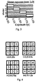
- the four shutter subsets are arranged to open sequentially as shown in Figure 3 .
- shutter subset 1 opens for 0.25 seconds, followed by subset 2 for the next 0.25 seconds, then subset 3 for another 0.25 seconds and finally subset 4 for a fourth 0.25 seconds.
- the total integration time T i for all the subsets is therefore 1.0 seconds, the individual exposure time of each pixel being T i /N (in this example, 0.25 seconds).
- the pixels underlying the open shutter elements are exposed to the light for the exposure time. However, the pixels are not all exposed simultaneously. Instead, the pixels are exposed sequentially, as the corresponding shutter elements open and close. Thus, the pixels underlying the shutter elements of subset 1 are exposed for the first period of 0.25 seconds, followed in turn by the pixels underlying the shutter elements in subsets 2, 3 and 4.
- each pixel integrates the charge generated when photons strike its surface. After the set integration time T i , the charge on all the pixels is digitised and the resulting digital image data is transferred from the sensor 4 to a memory device.
- the stored image data may be displayed either as a moving image (a movie) or a still image.
- a separate image is created from the image data captured by each pixel subset.
- image 1 is created from the image data captured by all of tho pixels in pixel subset 1, and represents the light incident on the sensor during the first period of 0.25 seconds.
- Image 2 is created from the image data captured by all the pixels in pixel subset 2, and represents the light incident on the sensor during the second period of point 0.25 seconds, and so on for images 3 and 4.
- the four images are then displayed sequentially, as a four frame video sequence.
- each pixel in the displayed low resolution image may be shifted in order to take into account that pixels collect data from slightly different, but known, locations.
- Each frame of the movie has an image size of 250,000 pixels, which is one quarter of the resolution of the entire sensor. We refer to these as low resolution (“lo-res”) images to distinguish them from the high resolution (“hi-res”) images generated by using the full pixel set.
- this process may be repeated one or more times, with multiple data sets being captured at a rate of one data set every T i seconds, and the captured lo-res images can subsequently be displayed in sequence.
- the data from all the pixels on the sensor is used to create a full frame, high resolution image.
- this will be a one megapixel image. This can be achieved by combining the data from all four lo-res images to create the single hi-res image.
- the location of pixels in each subset does not have to follow a regular pattern as shown in Figure 2 .
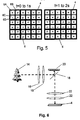
- An apparently random location within the shutter group can be chosen by implementing a numerical scheme, which uses a random number generator with a user supplied seed value and shuffles the location of each pixel within the exposure group. This is illustrated in Figure 5 , for a hypothetical array 4 of 6x6 pixels, with a pixel group size of 4.
- a numerical scheme generates a shuffled sequence of integers so that pixel groups still expose each pixel in the group for a subinterval of the total integration time as before, but the timing is given by the shuffled sequence.
- the un-shuffled sequence of integers ((1,2,3,4),(1,2,3,4),(1,2,3,4).7) indicates that the pixel 6A located at the top left of the first shutter group opens between 0-0.25s, the pixel 6B located at the top right of the first shutter group opens between 0.25-0.5s, and so on. Since the values repeat with a regular pattern, the exposure time for each pixel group is the same.
- the shuffled sequence ((3,2,1,4),(4,1,2,3),(2,3,1,4)...) illustrated in Figure 5 indicates that the top left most pixel 6A of the first shutter group opens between 0.5-0.75s, the top right pixel 6B of the first shutter group opens between 0.25-0.5s, the bottom left pixel 6C of the first shutter group opens between 0-0.25s, and the bottom right pixel 6D of the first shutter group opens between 0.75-1.0s.
- the second exposure group has a different sequence of opening times: the top left pixel of the second group opens between 0.75 and 1.0s, the top right pixel opens between 0 and 0.25s, and so on. Further, the sequence is not repeated for sequential frames: the pattern of exposures for 0 to 1s is different than that from 1 to 2s, and for each frame thereafter, depending on the length of the shuffled sequence.
- the randomized shutter scheme has two advantages. First, the location of each pixel in the low-resolution image is randomly assigned, even though the average distance between the pixels is the same. The advantages of having randomly distributed pixels vs. a regular under-sampled array for image reconstruction is well explained in United States Patent 4574311 , Random Array Sensing Devices, Resnikoff, Poggio, and Sims. Second, the low-resolution image sequence can only be recovered if the shuffled sequence of integers giving the correct timing is known. If the shuffled sequence is generated by an algorithm that incorporates a random number generating algorithm which is given a key, then the image sequence can only be recovered if the key is supplied by the person viewing the image sequence. This allows image sequences to be encrypted and protected from unauthorized viewing.
- shutter groups can have irregular polygonal shapes. Shutter groups can therefore cover regions of interest exactly, while excluding unnecessary pixels.
- An example of a possible use is in the life sciences, where a user may wish to monitor the activity of a small number of cells in a microscopic field of view. The user can draw a polygonal shape around the cells of interest, and an algorithm can divide the pixels within these shapes into groups which will be exposed at different times.
- the image may contain some "motion blur".
- the amount of motion blur will generally be greater than with a conventional still camera sensor in which all the pixels are exposed simultaneously, since the total integration time is greater than the exposure time of the individual pixels.
- the image quality will be substantially equal to that of a conventional sensor.
- a "movie/still” mode in which the shutter elements are actuated sequentially as described above, or a "still-only” mode in which all the shutter elements operate simultaneously.
- movie/still mode the captured los-res images can be viewed either sequentially as a movie, or together as a hi-res still image (possibly with some motion blur).
- still-only mode the motion blur will be equivalent to that of a conventional sensor, but because a set of time-separated lo-res images will not then be captured the possibility of viewing the images sequentially as a movie will not be available.
- a set number of pixels can be used to obtain a blur free high res. image, while the remainder can be used for obtaining a series of low res. images as previously described.
- the number of pixels for the high res. low blur image can be selected by the user in order to ensure the desired picture quality. For example, 50% of the pixels can be devoted to create a high resolution blur free image, where the pixels of this subgroup are distributed over the entire array. These pixels would be exposed simultaneously, for a short time equal to the optimal exposure time for a blur free image set by the user. The remaining pixels would be divided into N-1 groups as before, and exposed sequentially to generate a movie sequence.
- the distribution of the pixels in the high resolution group can be regular (for example, every second pixel), or the pixels can be randomly distributed, or pseudo randomly distributed (so that the average density over a defined sub area of pixels is constant, but individual pixels within that area are chosen using a known random distribution). Missing pixels in the high resolution image can be compensated for by using any of a variety of available signal processing techniques.
- the advantages of having randomly distributed pixels vs. a regular under-sampled array for image reconstruction is well explained in United States Patent 4574311 , Random Array Sensing Devices, Resnikoff, Poggio, and Sims.
- a multi-resolution image can be constructed by having part of the scene imaged using shutter groups of different sizes.
- the top half of the detector can be imaged using a shutter group of size 4 (so that four low res images are collected during acquisition of a full frame) and the bottom of the detector can be imaged using a shutter group of size 9 (so that nine low-res images are collected during the acquisition of a full frame).
- any number of different frame groups can be used based on user requirements. Possible uses include monitoring multiple moving objects in a scene, and allowing optimal settings (frame rate vs. resolution) to be employed on a per object basis. Shutter group size and geometry can also be dynamically changed, on a frame by frame basis, in order to account for changes in the imaged scene.
- the size of the shutter elements may be selected so that each shutter element controls the exposure of more than one pixel.
- the effective size of each shutter element would then be larger than an individual pixel. This will allow use of a shutter device having fewer shutter elements than there are pixels.
- each shutter element may be effectively smaller than an individual pixel, the exposure of each pixel then being controlled by multiple shutter elements. This may in certain circumstances aid in focussing, since the different shutters can be used to account for axial distortion in the lenses. It may also be possible to increase the spatial resolution of the sensor by opening different set of shutters with each frame.
- the interval between the successive exposures used to create the embedded lo-res images is equal to the duration of the individual exposures.
- the next exposure therefore starts as the previous one ends, and the total integration time Ti is equal to Nt, where N is the number of pixel subsets and t is the exposure time for the individual pixels.
- the interval between the exposures and the exposure time may be adjusted so that the exposure times overlap or are spaced apart. This would allow the user to compensate for motion blur or low light conditions. For example, instead of using exposure times of 0.25 seconds as illustrated in Figure 3 , the exposure time may be reduced to 0.15 seconds.
- the exposure timings of the individual pixel subsets may be as follows: pixel subset 1 from 0 to 0.15 seconds, pixel subset 2 from 0.25 to 0.4 seconds, pixel subset 3 from 0.5 to 0.65 seconds and pixel subset 4 from 0.75 to 0.9 seconds.
- the total integration time will then be less than Nt.
- the exposure time can be increased to 0.4 seconds, the individual exposure timings then being as follows: pixel subset 1 from 0 to 0.4 seconds, pixel subset 2 from 0.25 to 0.65 seconds, pixel subset 3 from 0.5 to 0.9 seconds and pixel subset 4 from 0.75 to 1.15 seconds.
- pixel subset exposures overlap (1 overlaps with 2, 2 overlaps with 3, 3 overlaps with 4 and 4 overlaps with 1).
- the exposure interval may therefore be optimised according to the speed at which the subject is changing or moving.
- the pixel subsets instead of exposing the pixel subsets sequentially for only a small fraction of the total integration time, they may all be exposed for the full integration time T i , apart from a short transient period in which the light is blocked.
- This blocked period may be applied to each of the pixel subsets in turn, and the pixel values for the blocked time period can be estimated since there will be a set of N linear equations with N unknowns.
- the transient blocking period may for example be equal to T i /N, where T i is the total integration time and N is the number of pixel subsets.
- the exposure time for each individual pixel will then be equal to T i - T i /N, which approaches the full integration time T i for large values of N.
- the process has the advantage that in low light situations the image brightness for the full resolution frame approaches that of a frame taken with a conventional sensor.
- a randomly accessible LCD pixel level shutter array 8 is formed directly on the surface of the sensor array 4, which may for example be a CCD, CMOS or EMCCD device.
- the shutter array 8 may for example be a ferro-electric shutter device, which is capable of rapid changes in transmittance, thus exposing the underlying pixels to the incident light.
- a liquid crystal on silicon (LCOS) device can be used to reflect light to pixels as shown in figure 6 .
- Light from an object 14 is focussed by objective lenses 16 and reflected by a polarizing beam filter (or splitter) 18 onto a LCOS device 20, which reflects back polarized light in a user selectable pattern.
- This light passes through the beam splitter 18 and is focussed through collector lenses 22 onto a sensor 4 comprising a CCD detector.
- LCOS liquid crystal display
- DMD digital light processing unit
- the intensity values of in register pixels can be summed to generate a bright high resolution image.
- the shutter array 8 is spaced away from the CCD sensor device 4. Two sets of lenses are provided, the first set 24 being positioned in front of the shutter array 8 and arranged to focus an image of a subject 14 onto the shutter array.
- the second set of lenses 26 is located between the shutter array and the CCD sensor 4, and focuses the image formed in the plane of the shutter array onto the CCD sensor 4.
- the shutter array 8, which may for example be a ferroelectric LCD shutter array, thus serves to block light from the sensor array or allow light through to the sensor array, as required.
- high speed digital mirror device (DMD) 28 is arranged in the focal plane of a pair of objective lenses 30, which focus an image of an object 14 onto the surface of the DMD 28.
- the DMD 28 comprises a randomly accessible array of micro mirrors 32 that can be tilted back and forth by applying a driving voltage.
- a DMD array with 0.7" array of 1024 by 768 bistable micro mirrors capable of 16,000 full array mirror patterns/second is readily available and suitable for this use.
- the micro mirrors 32 can be toggled to a first angle at which they reflect the incident light towards a CCD sensor array 34, or to a second angle at which they reflect the light towards a light trap 36.
- a second set of lenses 38 is provided between the DMD 28 and the sensor 34, to refocus the image formed on the surface of the DMD onto the sensor 34.
- the DMD 28 can thus be operated to control the exposure of the individual pixels to the incident light.
- the sensor 40 in Figure 9 is divided into columns of active pixels 42, which are separated by columns of masked pixels 44.
- the masked pixels 44 are shielded from incident light by an opaque mask and do not therefore contribute directly to the image acquisition process. Instead, they serve as charge storage devices, each masked pixel 44 being linked to an adjacent active pixel 42. In operation, charge is shifted on a column by column basis from the unmasked columns of active pixels to the masked columns of inactive pixels.
- the sensor may for example be arranged as shown in Figure 9 with four subsets of pixels, which are here numbered pixel subset 1, pixel subset 2, pixel subset 3 and pixel subset 4.
- the pixel subsets are arranged in exposure groups 46, each exposure group including one column of pixel elements from each pixel subset.
- the pixels within one pixel subset are exposed to light for the exposure time, and the charge is then transferred to the adjacent column of masked pixels for digitising. This process is repeated for each of the pixel subsets in turn, thus forming four time-dependent lo-res images within each hi-res full frame image.
- These embedded lo-res images can be viewed in sequence as a movie, or combined together to form a single high resolution still image.
- the unmasked pixels can once again be exposed to the light to capture the next image.
- the charge on any pixel on column n at any subinterval can be calculated by subtraction of the adjacent pixel in the previous column.
- CMOS detector it may be possible to implement a process that uses transient blocking of light by moving charge from a pixel under a mask and then back to the integrating pixel.
- Another possibility involves using a CMOS detector to store charge from pixels at different time points within the acquisition of a single hi-res image.
- the sensor device 50 comprises a 640x640 pixel array in which the pixels 52 and the corresponding shutter elements (not shown) are arranged in one hundred pixel groups 54, each pixel group having sixty-four pixels set out in an 8x8 array.
- the sixty-four pixels 52 within each group 54 are exposed sequentially, for example in the sequence illustrated by the numerals 1-64 marked on the pixels 52 in Fig. 10 .
- the pixels within each of the pixel groups 54 are exposed in the same sequence, and that this sequence is designed to ensure that consecutively exposed pixels are separated spatially from one another.
- the first pixel to be exposed is in column 1, row 1, the second pixel is in column 5, row 1, the third is in column 1, row 5, and so on.
- each full frame image captured by the sensor device can be displayed either as a hi-res 640x640 pixel still image or as a sequence of sixty-four lo-res 80x80 pixel images.
- pixels 1 through 4 can be coalesced into one subset (since they are exposed within a short time interval of each other), pixels 5 through 8 can be similarly coalesced, and so on, giving rise to sixteen pixel subsets within the original sixty-four pixel group.
- a similar operation can be carried out in all the pixel groups, which will result in a sixteen frame, 160x160 pixel image sequence.
- pixels 1-16 are coalesced to form a first subset
- pixels 17-32 are coalesced to form a second subset
- pixels 33-48 hatchched background
- pixels 49-64 are coalesced to form a fourth subset.
- Lo-res images from these coalesced subsets can be generated to provide a four-frame, 320x320 pixel image sequence.
- D a positive integer equal to the dimension of each image in the image sequence (width and height)
- m a positive integer.
- the pixel group size can be made as large as the total number of pixels giving one group, which would allow the user to coalesce temporally adjacent pixels to obtain an optimal image sequence.
- the invention may be implemented within a camera that is intended primarily for capturing still images, to provide the possibility of capturing movies at a relatively high resolution and frame rate.
- a camera that can take a sequence of 8.2 megapixel images at a rate of five frames per second would be capable of providing a movie sequence of 0.8 megapixel images at a frame rate of fifty frames per second.
- An advantage to the consumer is that the original high resolution photographs are conserved, and the data storage requirement (image size in memory) is the same as a conventional digital camera.
- Applications may include video acquisition and security camera operation, allowing the simultaneous capture of high resolution images for scene detail and low resolution image sequences.
- This camera 60 includes a lens 62 that focuses an image onto a CCD sensor 64.
- An LCD shutter array 66 is mounted in front of the sensor 64 and controls exposure of the individual pixels to the incident light. Operation of the LCD shutter array 66 is controlled by a central processor unit (CPU) 68, which is also connected to the sensor 64 in order to read data from the sensor. This data is stored in a memory device 70, for example a flash memory card.
- the camera includes a shutter release 72 and a control switch 74 that is linked to the CPU 68 and may be used to set, for example, the operational mode of the camera.
- These modes may for example include “movie/still” mode in which the camera captures a set of time-separated lo-res images within each hi-res frame that may be viewed either as a movie or a high resolution still image, or "still-only” mode in which the pixels are all exposed simultaneously to form a still image with minimal motion blur.
- the camera may also include other conventional features, such as a viewfinder, a display unit for checking settings or viewing captured images, lens controls for controlling the aperture, focal length and focussing of the lens 62, a flash unit, a data output port and so on.
- the significant demand for high temporal resolution detectors has resulted in specialized, high priced camera systems that either have very low spatial resolution (e.g. the Marconi CCD39, which has 80x80 pixels and can run at 1KHz) or a low dynamic range (e.g. intensified CCDs and EMCCDs, which use a gain boosting mechanism to compensate for the increased frame read noise that occurs at high frame rates, at the expense of a dramatic reduction in intrascene dynamic range).
- the present invention allows a conventional low noise, high resolution CCD to be used for high speed imaging.
- High resolution megapixel scientific grade CCDs can integrate single frames in 0.1 to 1 seconds (depending on bit depth and internal camera circuitry).
- Conventional methods can increase read speed in most scientific grade high resolution CCD and EMCCD systems using a technique called on chip binning where adjacent pixels are 'grouped' on chip, and can be read out more rapidly.
- Speed gains are often in the order of N for a NxN binning scheme. This is a factor of N less that what can be accomplished with the technology proposed here.
- the binned image does not contain high spatial resolution data.
- the new technology will make it possible to define arbitrarily shaped exposure groups (non rectangular), which will allow researchers to optimize speed and resolution depending on the exact features of the scene being imaged.
- Very high frame rates are attainable if a low spatial resolution is acceptable.
- the proposed technology will allow scenes to be imaged at a high dynamic range with sub millisecond frame times. This is significantly faster than can currently be achieved with low noise, high dynamic range scientific area detectors.
- S/N signal/noise
- this technology can be used to further improve spatial and temporal resolutions by enabling the use of novel sampling protocols.
- a possible example is the use of irregular sampling times, at the pixel level, to improve temporal resolution (via the Lomb Periodogram). This is not at present possible with available imaging technologies.
- the present invention can address this issue by varying the number of shutter groups (and hence the temporal and spatial resolution as well as total exposure time) within one frame, so as to optimise imaging of several objects within the scene.
- objects closer to the camera are proportionately larger, reducing the spatial resolution requirements and allowing for increased temporal resolution.
- the size of the shutter groups can be chosen using a priori knowledge of the scene (for example, vehicles monitored travelling on a highway by an elevated camera facing the direction of traffic flow would become proportionately smaller toward the top of the image, allowing the use of a gradation of shutter group sizes to maintain the average number of pixels per car).
- the size of the shutter groups can be chosen dynamically using algorithmic methods (for example, by obtaining the optical flow from motion blur in a static image, as described in Berthold and Shunck, "Determining Optical Flow", Technical Report, MIT, 1980 ) or range finding equipment (e.g. laser range finders or similar).
- algorithmic methods for example, by obtaining the optical flow from motion blur in a static image, as described in Berthold and Shunck, "Determining Optical Flow", Technical Report, MIT, 1980
- range finding equipment e.g. laser range finders or similar.
- regions of interest can be imaged at different resolutions independent of the shutter group pattern used in the majority of the image.
- a camera monitoring traffic could obtain high spatial resolution images of the licence plates of vehicles by controlling the exposure time of an appropriately chosen rectangle of pixels, while monitoring vehicle motion with low spatial resolution.
- Vehicle speed and licence plate detection could be accomplished without a radar device in such a system by using the camera to continuously monitor vehicle motion at low spatial resolution (using sufficiently large shutter groups).
- a computer algorithm would calculate vehicle speed and dynamically change the shutter groups to image either the whole scene or just the licence plates at high spatial resolution when required.
Landscapes
- Engineering & Computer Science (AREA)
- Multimedia (AREA)
- Signal Processing (AREA)
- Studio Devices (AREA)
- Transforming Light Signals Into Electric Signals (AREA)
Description
- The present invention relates to an image capture device and a method of capturing images, and in particular but not exclusively to a device and method for capturing both still and moving images (movies).
- Electronic cameras are generally divided into two broad categories: still cameras and video cameras. However, there is a degree of overlap between the two types of camera.
- For example, some "video" cameras are capable of capturing both movies and still images.
- On the other hand, some still cameras are provided with a "movie" function, which allows the camera to capture a sequence of images. These images can subsequently be shown as a movie. This invention is concerned primarily (but not exclusively) with the latter type of camera.
- Electronic cameras generally include an image capture device or sensor having an array of photosensitive detectors or picture elements (pixels). A moving image or movie can be captured by recording a sequence of images detected by the sensor.
- The rate at which a sequence of images can be captured (the frame rate) depends in part on the size of the sensor (that is, the number of pixels in the array), and is limited by the rate at which data can be read (digitised) from the sensor. Reading information from an imaging sensor at high speed introduces noise (read noise), which lowers the signal quality of the image. Accordingly, if the sensor has a large number of pixels, the frame rate will generally be rather slow. Smaller sensors with fewer pixels may provide a higher frame rate, but the resolution of the image will be correspondingly reduced.
-
JP2006238205A -
US2003/0052989A1 describes a light shuttering module for a digital imaging sensor, which includes a shutter device having a plurality of individually-addressable shutter elements. -
US2007/0223887A1 describes a recording process that records low resolution video data while obtain a high resolution image in a window region being a portion of an entire image. -
US2005/0168589A1 describes a method for processing an image with an image capturing device, which involves retrieving and storing a subset of image data and generating an image from the subset of data. -
US2005/0224695A1 describes an optical sensor that includes a spatial light modulator, a photodetector having a plurality of photosensitive areas after it has been phase modulated, and a photosensor selecting section that selects and activates an area of the a selected photosensor area. -
US2006/0158537A1 describes an imaging apparatus with an imaging element equipped with a colour filter array, which generates full colour data by obtaining weighting coefficients based on the basis of a relative relationship between positions of a lattice pattern and position information of the pixel signals. - It is an object of the present invention to provide an image capture device and a method of capturing images that mitigate at least some of the aforesaid disadvantages.
- According to one aspect of the invention there is provided an image capture device for capturing a movie comprising a sequence of images, the image capture device including a sensor having an active area comprising a set of pixels, each pixel providing in use data that represents the exposure of that pixel, and a data storage device for storing data from the pixels, said set of pixels comprising a plurality of pixel subsets and a plurality of pixel groups, wherein the pixel groups cover substantially the entire active area of the sensor and each pixel group is located in a different region of the sensor and contains at least one pixel from each pixel subset, and wherein each pixel subset includes pixels from substantially the entire active area of the sensor, and said image capture device including a control device for controlling the exposure of the pixel subsets, characterised by said control device being constructed and arranged to expose the pixel subsets sequentially to capture a plurality of time-separated lo-res images, each said lores image comprising the data from a different pixel subset, and wherein after all of the pixels have been exposed the image capture device digitizes a charge on all the pixels to provide a set of digital data and transfers said digital data to the data storage device.
- The invention allows a set of time-separated low resolution ("lo-res") images to be embedded within each high resolution ("hi-res") image. The embedded lo-res images can then be viewed in sequence as a movie, or the data in those images can be combined to form a single hi-res image. Movies and still images can thus be captured simultaneously. The device allows movies to be captured at much higher frame rates than can currently be achieved with equivalent sensor devices and, although the spatial resolution of the lo-res images is lower than that of the hi-res image, it is still sufficient for many purposes. The balance of resolution versus frame rate can be easily adjusted. Furthermore, the still images can be captured with no loss of spatial resolution and no significant increase in the data storage requirements of the device.
- Advantageously, the image capture device is constructed and arranged to capture a hi-res image by combining the data within said plurality of lo-res images.
- Each pixel subset includes pixels from substantially the entire active area of the sensor. Thus, each lo-res image formed from one such a pixel subset will be a full frame image. In addition, at least one pixel subset may include pixels from less than the entire active area of the sensor. This allows different parts of the scene to be imaged at different spatial and temporal resolutions, which may be useful in certain security camera or robotic systems.
- The image capture device may include a shutter array comprising a plurality of shutter elements, each for controlling the exposure of an individual pixel. Alternatively, each shutter element may control the exposure of more than one pixel, being effectively larger than a pixel. Alternatively, each shutter element may be effectively smaller than an individual pixel, the exposure of each pixel then being controlled by multiple shutter elements.
- The shutter array may comprise a plurality of shutter elements of variable opacity or variable reflectivity. The shutter array may be mounted on the active area of the sensor or in front of the sensor (preferably with a focussing device between the shutter array and the sensor).
- Alternatively, the shutter array may comprise a plurality of shutter elements of variable orientation. The shutter elements may comprise mirrors, which can be oriented to reflect light towards or away from the sensor.
- The image capture device preferably includes a control device for controlling operation of the shutter array. This may control, for example, the number of pixel subsets into which the full set of pixels on the sensor is divided, the exposure times for the pixel subsets and the relative timing of those exposures, and the operational mode of the device (for example, movie/still mode or still-only mode). The control device may be constructed and arranged to actuate the shutter elements in a predefined, random or pseudo-random sequence, which can be reconstructed later to decode the high speed image sequence. The control device may also be arranged to provide an alternative operational mode in which the shutter elements are all activated simultaneously.
- In another preferred embodiment, each pixel is associated with a charge storage device to which charge may be transferred from the pixel, the image capture device including a control device for controlling the transfer of charge so as to capture said plurality of time-separated lo-res images. In this arrangement a shutter array is not required, so simplifying the construction of the device.
- According to another aspect of the invention there is provided a camera including an image capture device according to any one of the preceding statements of invention and a lens for focussing light onto the active area of the sensor.
- The camera may include a display device for displaying captured images, which is constructed and arranged to display either a single hi-res image or a sequence of lo-res images.
- Advantageously, the camera includes a control device for controlling the exposure of the pixel subsets.
- According to another aspect of the invention there is provided a method of capturing a movie comprising a sequence of images using an image capture device that includes a sensor having an active area comprising a set of pixels, the method comprising exposing the sensor, storing data representing the exposure of each pixel, and capturing a plurality of time-separated lo-res images, wherein said set of pixels comprises a plurality of pixel subsets and a plurality of pixel groups, wherein the pixel groups cover substantially the entire active area of the sensor and each pixel group is located in a different region of the sensor and contains at least one pixel from each pixel subset, and wherein each pixel subset includes pixels from substantially the entire active area of the sensor, characterised in that exposing the sensor comprises exposing the pixel subsets sequentially, whereby each lo-res image comprises the data from a different one of said pixel subsets, and wherein after all of the pixel subsets have been exposed the charge on all the pixels is digitised to provide a set of digital data and said digital data is transferred to the data storage device.
- The method includes exposing the pixel subsets sequentially, preferably in a predefined, random or pseudo-random sequence. Alternatively, the pixel subsets may be exposed simultaneously, in order to capture a hi-res still image with minimal motion blur.
- The method may include creating a hi-res image by combining the data from a plurality of lo-res images and preferably displaying said hi-res image.
- The method may also include displaying a sequence of said time-separated lo-res images.
- Certain embodiments of the invention will now be described by way of example with reference to the accompanying drawings, in which:
-
Figure 1 is an orthogonal front view showing schematically an image capture device according to a first embodiment of the invention; -
Figure 2 is a front view showing at an enlarged scale a small portion of the image capture device; -
Figure 3 is a chart illustrating shutter exposure times for respective shutter elements in the image capture device ofFigure 2 ; -
Figure 4 illustrates how a sequence of images may be captured by the image capture device; -
Figure 5 is a front view of an image capture device, illustrating one example of an operating sequence; -
Figure 6 is a side view showing schematically the optical arrangement of an image capture device according to a second embodiment of the invention; -
Figure 7 is a side view showing schematically the optical arrangement of an image capture device according to a third embodiment of the invention; -
Figure 8 is a side view showing the optical arrangement of an image capture device according to a fourth embodiment of the invention; -
Figure 9 is a front view showing a small portion of an image capture device according to a fifth embodiment of the invention; -
Figure 10 is a front view showing at an enlarged scale a small portion of an image capture device according to a sixth embodiment of the invention, and -
Figure 11 is a schematic diagram illustrating the main components of a camera that includes an image capture device according to the invention. - An image capture device according to a first embodiment of the invention is shown in
Figures 1 to 4 . Theimage capture device 2 includes asensor 4 having an active area comprising a rectangular array of photosensitive picture elements (pixels) 6. Thesensor 4 may for example be a CCD or CMOS device, or equivalent. In this example, thesensor 4 is a one megapixel CCD, comprising a rectangular array that is 1000 pixels wide and 1000 pixels tall. The sensor may of course be larger or smaller than this and may have a different aspect ratio, and the pixels may be arranged in various different patterns. - Mounted immediately in front of the
sensor 4 is anelectronic shutter device 8, having an array of pixelsized shutter elements 10. Theshutter elements 10 are matched to and aligned with thepixels 6 of thesensor 4, so that each shutter element controls the exposure to light of the underlying pixel. Therefore, in this example theshutter device 8 has one millionshutter elements 10, arranged in a 1000 x 1000 array. Eachshutter element 10 may be actuated independently or simultaneously with one or more other shutter elements to expose the underlying pixel orpixels 6. - In this example the
shutter device 8 consists of a ferroelectric liquid crystal device, comprising an array of liquid crystal cells that can be made transparent or opaque by the application of a voltage. This allows theshutter elements 10 to operate very rapidly. As the mechanism has no moving parts, it is robust and reliable. Alternatively, any other shutter mechanism that can be controlled electronically and that provides the necessary pixel level shuttering may be used. - More generally, the
shutter device 8 contains A shutter elements, which are divided into N subsets, which we will callsubset 1,subset 2 ... subset N. Each subset contains A/N shutter elements. In this example, the shutter device has one million shutter elements (A) and four subsets (N) ofshutter elements 10, each subset containing 250,000 shutter elements. Thepixels 6 underlying theshutter elements 10 form corresponding pixel subsets. - The
shutter elements 10 of the different subsets are arranged inshutter groups 12, each shutter group containing one shutter element from each subset. In this example, as shown inFigure 2 , eachshutter group 12 contains fourshutter elements 10, which are arranged in a square with ashutter element 10A fromsubset 1 in the top left corner, ashutter element 10B fromsubset 2 in the top right corner,shutter element 10C fromsubset 3 in the bottom left corner andshutter element 10D fromsubset 4 in the bottom right corner. Theshutter device 8 thus comprises 250,000 such shutter groups. The pixels are similarly arranged in pixel subsets and groups, each group containing one pixel from each subset. The pixel groups cover substantially the entire active surface of thesensor 4 and each pixel subset therefore includes pixels from substantially the entire active area of the sensor. - The shutter elements in each subset are electronically linked so that all the shutter elements in that subset open and close simultaneously, as determined by control electronics. In this example, the four shutter subsets are arranged to open sequentially as shown in
Figure 3 . Thus,shutter subset 1 opens for 0.25 seconds, followed bysubset 2 for the next 0.25 seconds, thensubset 3 for another 0.25 seconds and finallysubset 4 for a fourth 0.25 seconds. The total integration time Ti for all the subsets is therefore 1.0 seconds, the individual exposure time of each pixel being Ti/N (in this example, 0.25 seconds). - During each exposure time, the pixels underlying the open shutter elements are exposed to the light for the exposure time. However, the pixels are not all exposed simultaneously. Instead, the pixels are exposed sequentially, as the corresponding shutter elements open and close. Thus, the pixels underlying the shutter elements of
subset 1 are exposed for the first period of 0.25 seconds, followed in turn by the pixels underlying the shutter elements insubsets - During exposure, each pixel integrates the charge generated when photons strike its surface. After the set integration time Ti, the charge on all the pixels is digitised and the resulting digital image data is transferred from the
sensor 4 to a memory device. - The stored image data may be displayed either as a moving image (a movie) or a still image. To display the image data as a movie, a separate image is created from the image data captured by each pixel subset. Thus, as illustrated in
Figure 4 ,image 1 is created from the image data captured by all of tho pixels inpixel subset 1, and represents the light incident on the sensor during the first period of 0.25 seconds.Image 2 is created from the image data captured by all the pixels inpixel subset 2, and represents the light incident on the sensor during the second period of point 0.25 seconds, and so on forimages - If an extended video sequence is required, this process may be repeated one or more times, with multiple data sets being captured at a rate of one data set every Ti seconds, and the captured lo-res images can subsequently be displayed in sequence.
- To display a still image, the data from all the pixels on the sensor is used to create a full frame, high resolution image. In the example, this will be a one megapixel image. This can be achieved by combining the data from all four lo-res images to create the single hi-res image.
- The location of pixels in each subset does not have to follow a regular pattern as shown in
Figure 2 . An apparently random location within the shutter group can be chosen by implementing a numerical scheme, which uses a random number generator with a user supplied seed value and shuffles the location of each pixel within the exposure group. This is illustrated inFigure 5 , for ahypothetical array 4 of 6x6 pixels, with a pixel group size of 4. A numerical scheme generates a shuffled sequence of integers so that pixel groups still expose each pixel in the group for a subinterval of the total integration time as before, but the timing is given by the shuffled sequence. - In
Figure 2 , the un-shuffled sequence of integers ((1,2,3,4),(1,2,3,4),(1,2,3,4)....) indicates that thepixel 6A located at the top left of the first shutter group opens between 0-0.25s, thepixel 6B located at the top right of the first shutter group opens between 0.25-0.5s, and so on. Since the values repeat with a regular pattern, the exposure time for each pixel group is the same. - In contrast, the shuffled sequence ((3,2,1,4),(4,1,2,3),(2,3,1,4)...) illustrated in
Figure 5 indicates that the top leftmost pixel 6A of the first shutter group opens between 0.5-0.75s, the topright pixel 6B of the first shutter group opens between 0.25-0.5s, the bottomleft pixel 6C of the first shutter group opens between 0-0.25s, and the bottomright pixel 6D of the first shutter group opens between 0.75-1.0s. The second exposure group has a different sequence of opening times: the top left pixel of the second group opens between 0.75 and 1.0s, the top right pixel opens between 0 and 0.25s, and so on. Further, the sequence is not repeated for sequential frames: the pattern of exposures for 0 to 1s is different than that from 1 to 2s, and for each frame thereafter, depending on the length of the shuffled sequence. - The randomized shutter scheme has two advantages. First, the location of each pixel in the low-resolution image is randomly assigned, even though the average distance between the pixels is the same. The advantages of having randomly distributed pixels vs. a regular under-sampled array for image reconstruction is well explained in United States Patent
4574311 , Random Array Sensing Devices, Resnikoff, Poggio, and Sims. Second, the low-resolution image sequence can only be recovered if the shuffled sequence of integers giving the correct timing is known. If the shuffled sequence is generated by an algorithm that incorporates a random number generating algorithm which is given a key, then the image sequence can only be recovered if the key is supplied by the person viewing the image sequence. This allows image sequences to be encrypted and protected from unauthorized viewing. - In addition to having rectangular geometries as shown in
Figure 2 andFigure 5 , shutter groups can have irregular polygonal shapes. Shutter groups can therefore cover regions of interest exactly, while excluding unnecessary pixels. An example of a possible use is in the life sciences, where a user may wish to monitor the activity of a small number of cells in a microscopic field of view. The user can draw a polygonal shape around the cells of interest, and an algorithm can divide the pixels within these shapes into groups which will be exposed at different times. - If the subject imaged by the sensor was moving during the exposure time, the image may contain some "motion blur". The amount of motion blur will generally be greater than with a conventional still camera sensor in which all the pixels are exposed simultaneously, since the total integration time is greater than the exposure time of the individual pixels. However, for subjects having little or no movement, the image quality will be substantially equal to that of a conventional sensor.
- Alternatively, it may be possible to select various different image capture modes, such as a "movie/still" mode in which the shutter elements are actuated sequentially as described above, or a "still-only" mode in which all the shutter elements operate simultaneously. In movie/still mode the captured los-res images can be viewed either sequentially as a movie, or together as a hi-res still image (possibly with some motion blur). In still-only mode the motion blur will be equivalent to that of a conventional sensor, but because a set of time-separated lo-res images will not then be captured the possibility of viewing the images sequentially as a movie will not be available.
- Alternatively, a set number of pixels can be used to obtain a blur free high res. image, while the remainder can be used for obtaining a series of low res. images as previously described. The number of pixels for the high res. low blur image can be selected by the user in order to ensure the desired picture quality. For example, 50% of the pixels can be devoted to create a high resolution blur free image, where the pixels of this subgroup are distributed over the entire array. These pixels would be exposed simultaneously, for a short time equal to the optimal exposure time for a blur free image set by the user. The remaining pixels would be divided into N-1 groups as before, and exposed sequentially to generate a movie sequence. The distribution of the pixels in the high resolution group can be regular (for example, every second pixel), or the pixels can be randomly distributed, or pseudo randomly distributed (so that the average density over a defined sub area of pixels is constant, but individual pixels within that area are chosen using a known random distribution). Missing pixels in the high resolution image can be compensated for by using any of a variety of available signal processing techniques. The advantages of having randomly distributed pixels vs. a regular under-sampled array for image reconstruction is well explained in United States Patent
4574311 , Random Array Sensing Devices, Resnikoff, Poggio, and Sims. - In addition to having shutter groups with the same number of pixels, a multi-resolution image can be constructed by having part of the scene imaged using shutter groups of different sizes. For example, the top half of the detector can be imaged using a shutter group of size 4 (so that four low res images are collected during acquisition of a full frame) and the bottom of the detector can be imaged using a shutter group of size 9 (so that nine low-res images are collected during the acquisition of a full frame).
- In principle any number of different frame groups can be used based on user requirements. Possible uses include monitoring multiple moving objects in a scene, and allowing optimal settings (frame rate vs. resolution) to be employed on a per object basis. Shutter group size and geometry can also be dynamically changed, on a frame by frame basis, in order to account for changes in the imaged scene.
- In certain circumstances, the size of the shutter elements may be selected so that each shutter element controls the exposure of more than one pixel. The effective size of each shutter element would then be larger than an individual pixel. This will allow use of a shutter device having fewer shutter elements than there are pixels. Alternatively, each shutter element may be effectively smaller than an individual pixel, the exposure of each pixel then being controlled by multiple shutter elements. This may in certain circumstances aid in focussing, since the different shutters can be used to account for axial distortion in the lenses. It may also be possible to increase the spatial resolution of the sensor by opening different set of shutters with each frame.
- A practical example will now be described in which the invention is implemented in a digital SLR camera having an 8.2 megapixel sensor with dimensions of 2340 x 3500 pixels. An equivalent conventional camera is currently available, which is capable of capturing full frame images at a rate of five frames per second. If the present invention were implemented in that camera it could for example capture ten 0.82 megapixel lo-res images within each full frame image. Those lo-res images could then be viewed sequentially in movie mode at a rate of fifty frames per second, and a frame size of 738 x 1108 pixels. Alternatively, each set of lo-res images can be recombined to create a high resolution 8.2 megapixel still image.
- It will of course be apparent that by embedding more low resolution images within each full frame image even higher frame rates can be obtained. Alternatively, if a lower frame rate is adequate, a higher resolution movie can be captured.
- In the process described above, the interval between the successive exposures used to create the embedded lo-res images is equal to the duration of the individual exposures. The next exposure therefore starts as the previous one ends, and the total integration time Ti is equal to Nt, where N is the number of pixel subsets and t is the exposure time for the individual pixels. Alternatively, the interval between the exposures and the exposure time may be adjusted so that the exposure times overlap or are spaced apart. This would allow the user to compensate for motion blur or low light conditions. For example, instead of using exposure times of 0.25 seconds as illustrated in
Figure 3 , the exposure time may be reduced to 0.15 seconds. The exposure timings of the individual pixel subsets may be as follows:pixel subset 1 from 0 to 0.15 seconds,pixel subset 2 from 0.25 to 0.4 seconds,pixel subset 3 from 0.5 to 0.65 seconds andpixel subset 4 from 0.75 to 0.9 seconds. The total integration time will then be less than Nt. - As another example, the exposure time can be increased to 0.4 seconds, the individual exposure timings then being as follows:
pixel subset 1 from 0 to 0.4 seconds,pixel subset 2 from 0.25 to 0.65 seconds,pixel subset 3 from 0.5 to 0.9 seconds andpixel subset 4 from 0.75 to 1.15 seconds. In this case pixel subset exposures overlap (1 overlaps with 2, 2 overlaps with 3, 3 overlaps with 4 and 4 overlaps with 1). The exposure interval may therefore be optimised according to the speed at which the subject is changing or moving. - In another variant, instead of exposing the pixel subsets sequentially for only a small fraction of the total integration time, they may all be exposed for the full integration time Ti, apart from a short transient period in which the light is blocked. This blocked period may be applied to each of the pixel subsets in turn, and the pixel values for the blocked time period can be estimated since there will be a set of N linear equations with N unknowns. The transient blocking period may for example be equal to Ti/N, where Ti is the total integration time and N is the number of pixel subsets. The exposure time for each individual pixel will then be equal to Ti - Ti/N, which approaches the full integration time Ti for large values of N. While the low resolution images may contain errors as the intensity from each pixel is inferred from its neighbours, the process has the advantage that in low light situations the image brightness for the full resolution frame approaches that of a frame taken with a conventional sensor.
- Various practical implementations of the sensor device are shown in
Figures 1 ,6 ,7 and 8 . InFigure 1 , a randomly accessible LCD pixellevel shutter array 8 is formed directly on the surface of thesensor array 4, which may for example be a CCD, CMOS or EMCCD device. Theshutter array 8 may for example be a ferro-electric shutter device, which is capable of rapid changes in transmittance, thus exposing the underlying pixels to the incident light. - Alternatively, a liquid crystal on silicon (LCOS) device can be used to reflect light to pixels as shown in
figure 6 . Light from anobject 14 is focussed byobjective lenses 16 and reflected by a polarizing beam filter (or splitter) 18 onto aLCOS device 20, which reflects back polarized light in a user selectable pattern. This light passes through thebeam splitter 18 and is focussed throughcollector lenses 22 onto asensor 4 comprising a CCD detector. - Alternatively, if a reflective pixel level shutter is used (LCOS or DMD), light from a blocked pixel can be focussed on a second CCD detector, aligned to be in register with the first. This would allow the majority of the light during the CCD integration period to be captured.
- The intensity values of in register pixels can be summed to generate a bright high resolution image.
- In the arrangement shown in
Figure 7 , theshutter array 8 is spaced away from theCCD sensor device 4. Two sets of lenses are provided, thefirst set 24 being positioned in front of theshutter array 8 and arranged to focus an image of a subject 14 onto the shutter array. The second set oflenses 26 is located between the shutter array and theCCD sensor 4, and focuses the image formed in the plane of the shutter array onto theCCD sensor 4. Theshutter array 8, which may for example be a ferroelectric LCD shutter array, thus serves to block light from the sensor array or allow light through to the sensor array, as required. - In the arrangement shown in
Figure 8 , high speed digital mirror device (DMD) 28 is arranged in the focal plane of a pair ofobjective lenses 30, which focus an image of anobject 14 onto the surface of theDMD 28. TheDMD 28 comprises a randomly accessible array ofmicro mirrors 32 that can be tilted back and forth by applying a driving voltage. A DMD array with 0.7" array of 1024 by 768 bistable micro mirrors capable of 16,000 full array mirror patterns/second is readily available and suitable for this use. - The micro mirrors 32 can be toggled to a first angle at which they reflect the incident light towards a
CCD sensor array 34, or to a second angle at which they reflect the light towards alight trap 36. A second set oflenses 38 is provided between theDMD 28 and thesensor 34, to refocus the image formed on the surface of the DMD onto thesensor 34. TheDMD 28 can thus be operated to control the exposure of the individual pixels to the incident light. - The above examples all use dynamic masking, in which light is physically blocked from the pixels, for example by a LCD shutter device or a DMD array. Alternatively, it is possible to implement the invention using static on-chip masking, in which the effect of a physical mask is mimicked by transferring charge sequentially from the pixels onto masked charge-retaining portions of the sensor chip. An embodiment of a sensor that utilises this approach is illustrated schematically in
Figure 9 . - The
sensor 40 inFigure 9 is divided into columns ofactive pixels 42, which are separated by columns ofmasked pixels 44. Themasked pixels 44 are shielded from incident light by an opaque mask and do not therefore contribute directly to the image acquisition process. Instead, they serve as charge storage devices, eachmasked pixel 44 being linked to an adjacentactive pixel 42. In operation, charge is shifted on a column by column basis from the unmasked columns of active pixels to the masked columns of inactive pixels. The sensor may for example be arranged as shown inFigure 9 with four subsets of pixels, which are here numberedpixel subset 1,pixel subset 2,pixel subset 3 andpixel subset 4. The pixel subsets are arranged inexposure groups 46, each exposure group including one column of pixel elements from each pixel subset. - The pixels within one pixel subset are exposed to light for the exposure time, and the charge is then transferred to the adjacent column of masked pixels for digitising. This process is repeated for each of the pixel subsets in turn, thus forming four time-dependent lo-res images within each hi-res full frame image. These embedded lo-res images can be viewed in sequence as a movie, or combined together to form a single high resolution still image.
- As soon as the charge has been transferred onto the masked pixels, the unmasked pixels can once again be exposed to the light to capture the next image.
- An example of a static on-chip masking process using a frame transfer architecture is given below.
- Here we consider a frame transfer CCD with M columns, where a portion of the chip is exposed to light, and a single hi-res image is acquired every Ti seconds. Exposure groups consisting of N adjacent columns are assigned, where the nth column of each group is transferred to the masked region at the same time.
- Accumulated charge from every nth column on the CCD is rapidly transferred to the masked region at (n x Ti)/N, so that all columns are transferred within Ti seconds. This may be repeated so that each column of pixels integrates light for a total of T seconds, but at staggered times.
- The charge on any pixel on column n at any subinterval can be calculated by subtraction of the adjacent pixel in the previous column.
- As an example of the above scheme, consider a 1000 pixel wide imaging area divided into 250 exposure groups of four columns each, and a frame integration time of 1s. The first column of each exposure group is shifted to the masked region at t=0.25s, the second column is shifted at t=0.5s, the third column is shifted at t=0.75s and the fourth column is shifted at t=1s. Once the charge is shifted from any column, the pixels continue to integrate light, and are shifted to the masked region again after 1s (so column one is shifted at t=1.25s, 2.25s etc,
column 2 is shifted at t=1.5s, 2.5s etc). - Alternatively, it may be possible to implement a process that uses transient blocking of light by moving charge from a pixel under a mask and then back to the integrating pixel. Another possibility involves using a CMOS detector to store charge from pixels at different time points within the acquisition of a single hi-res image.
- Another possible implementation of the invention is illustrated in
Figure 10 . In this embodiment, thesensor device 50 comprises a 640x640 pixel array in which thepixels 52 and the corresponding shutter elements (not shown) are arranged in one hundredpixel groups 54, each pixel group having sixty-four pixels set out in an 8x8 array. In use, the sixty-fourpixels 52 within eachgroup 54 are exposed sequentially, for example in the sequence illustrated by the numerals 1-64 marked on thepixels 52 inFig. 10 . It may be noticed that in this embodiment, the pixels within each of thepixel groups 54 are exposed in the same sequence, and that this sequence is designed to ensure that consecutively exposed pixels are separated spatially from one another. In this example, the first pixel to be exposed is incolumn 1,row 1, the second pixel is incolumn 5,row 1, the third is incolumn 1,row 5, and so on. - By processing the output signals of the pixels in different combinations, it is possible to adjust both the frame rate and the resolution of the images captured by the sensor device by trading off spatial resolution against temporal resolution. For example, each full frame image captured by the sensor device can be displayed either as a hi-res 640x640 pixel still image or as a sequence of sixty-four lo-res 80x80 pixel images. Alternatively,
pixels 1 through 4 can be coalesced into one subset (since they are exposed within a short time interval of each other),pixels 5 through 8 can be similarly coalesced, and so on, giving rise to sixteen pixel subsets within the original sixty-four pixel group. A similar operation can be carried out in all the pixel groups, which will result in a sixteen frame, 160x160 pixel image sequence. - By further coalescing temporally adjacent pixels, additional combinations of temporal and spatial resolutions are possible. For example, in the arrangement depicted in
Figure 10 , pixels 1-16 (dotted background) are coalesced to form a first subset, pixels 17-32 (striped background) are coalesced to form a second subset, pixels 33-48 (hatched background) are coalesced to form a third subset, and pixels 49-64 (white background) are coalesced to form a fourth subset. Lo-res images from these coalesced subsets can be generated to provide a four-frame, 320x320 pixel image sequence. More generally, for a square N pixel sensor within a 'A' shutter element shutter device, a 4m element image sequence can be created if 4m * D2 = A, where D a positive integer equal to the dimension of each image in the image sequence (width and height) and m is a positive integer. This allows the user to decide on the optimal spatial and temporal resolution of the low-res image sequence after the images have been captured, providing that the original shutter group has enough elements. Of course, since the shutter elements in the coalesced subsets are not exposed at exactly the same time, images within the newly coalesced image sequence may have some distortion. For example, the coalesced four frame 320x320 pixel image sequence from the arrangement shown inFigure 10 would probably be less clear than a four element image sequence obtained as illustrated inFigures 2 to 4 . - Additional variants of the above scheme could use randomly positioned pixels, if the pixel group size is large enough to ensure a high likelihood of sequentially-exposed pixels being far apart. In principle the pixel group size can be made as large as the total number of pixels giving one group, which would allow the user to coalesce temporally adjacent pixels to obtain an optimal image sequence.
- Various applications of the invention are envisaged. Some of these will now be described.
- The invention may be implemented within a camera that is intended primarily for capturing still images, to provide the possibility of capturing movies at a relatively high resolution and frame rate. For example, as indicated above, a camera that can take a sequence of 8.2 megapixel images at a rate of five frames per second would be capable of providing a movie sequence of 0.8 megapixel images at a frame rate of fifty frames per second.
- An advantage to the consumer is that the original high resolution photographs are conserved, and the data storage requirement (image size in memory) is the same as a conventional digital camera. Applications may include video acquisition and security camera operation, allowing the simultaneous capture of high resolution images for scene detail and low resolution image sequences.
- The basic elements of a camera are illustrated schematically in
Figure 11 . Thiscamera 60 includes alens 62 that focuses an image onto aCCD sensor 64. AnLCD shutter array 66 is mounted in front of thesensor 64 and controls exposure of the individual pixels to the incident light. Operation of theLCD shutter array 66 is controlled by a central processor unit (CPU) 68, which is also connected to thesensor 64 in order to read data from the sensor. This data is stored in amemory device 70, for example a flash memory card. The camera includes ashutter release 72 and acontrol switch 74 that is linked to theCPU 68 and may be used to set, for example, the operational mode of the camera. These modes may for example include "movie/still" mode in which the camera captures a set of time-separated lo-res images within each hi-res frame that may be viewed either as a movie or a high resolution still image, or "still-only" mode in which the pixels are all exposed simultaneously to form a still image with minimal motion blur. The camera may also include other conventional features, such as a viewfinder, a display unit for checking settings or viewing captured images, lens controls for controlling the aperture, focal length and focussing of thelens 62, a flash unit, a data output port and so on. - The significant demand for high temporal resolution detectors has resulted in specialized, high priced camera systems that either have very low spatial resolution (e.g. the Marconi CCD39, which has 80x80 pixels and can run at 1KHz) or a low dynamic range (e.g. intensified CCDs and EMCCDs, which use a gain boosting mechanism to compensate for the increased frame read noise that occurs at high frame rates, at the expense of a dramatic reduction in intrascene dynamic range). The present invention allows a conventional low noise, high resolution CCD to be used for high speed imaging.
- Additional advantages are discussed below.
- At present, there is no imaging modality that allows true simultaneous high temporal and high spatial resolution imaging. This technique can readily be applied to many biological problems. For example, one could monitor heart muscle motion at a high spatial resolution, and heart electrical activity at a high temporal resolution.
- High resolution megapixel scientific grade CCDs can integrate single frames in 0.1 to 1 seconds (depending on bit depth and internal camera circuitry). Conventional methods can increase read speed in most scientific grade high resolution CCD and EMCCD systems using a technique called on chip binning where adjacent pixels are 'grouped' on chip, and can be read out more rapidly. Speed gains are often in the order of N for a NxN binning scheme. This is a factor of N less that what can be accomplished with the technology proposed here. In addition, the binned image does not contain high spatial resolution data.
- The new technology will make it possible to define arbitrarily shaped exposure groups (non rectangular), which will allow researchers to optimize speed and resolution depending on the exact features of the scene being imaged.
- Very high frame rates are attainable if a low spatial resolution is acceptable. The proposed technology will allow scenes to be imaged at a high dynamic range with sub millisecond frame times. This is significantly faster than can currently be achieved with low noise, high dynamic range scientific area detectors.
- Improved signal/noise (S/N): an additional important advantage is that the proposed technology allows slower whole frame readout rates than is possible using on chip binning at equivalent frame rates. This may result in a significant improvement in S/N as read noise dominates signal quality at higher speeds.
- It is anticipated that this technology can be used to further improve spatial and temporal resolutions by enabling the use of novel sampling protocols. A possible example is the use of irregular sampling times, at the pixel level, to improve temporal resolution (via the Lomb Periodogram). This is not at present possible with available imaging technologies.
- Cameras that are used to monitor a changing 3D scene, which are common in surveillance applications and robotics/machine vision, must contend with several challenges. One issue is that if an object moves relative to the camera, the magnitude of movement of the image across the sensor will be inversely proportional to the distance of the object from the camera. This will cause motion blur to be more pronounced for objects close to the camera, obscuring necessary detail. For example, surveillance of a group of walking people on a street or in a building lobby would produce blurred images of their faces if they are close to the camera. Decreasing the shutter time for the whole image would potentially degrade image quality for objects far from the camera, as the total light collected from far objects will be less.
- The present invention can address this issue by varying the number of shutter groups (and hence the temporal and spatial resolution as well as total exposure time) within one frame, so as to optimise imaging of several objects within the scene. Advantageously, objects closer to the camera are proportionately larger, reducing the spatial resolution requirements and allowing for increased temporal resolution. The size of the shutter groups can be chosen using a priori knowledge of the scene (for example, vehicles monitored travelling on a highway by an elevated camera facing the direction of traffic flow would become proportionately smaller toward the top of the image, allowing the use of a gradation of shutter group sizes to maintain the average number of pixels per car). Alternatively, the size of the shutter groups can be chosen dynamically using algorithmic methods (for example, by obtaining the optical flow from motion blur in a static image, as described in Berthold and Shunck, "Determining Optical Flow", Technical Report, MIT, 1980) or range finding equipment (e.g. laser range finders or similar).
- Additionally, specific regions of interest can be imaged at different resolutions independent of the shutter group pattern used in the majority of the image. For example, a camera monitoring traffic could obtain high spatial resolution images of the licence plates of vehicles by controlling the exposure time of an appropriately chosen rectangle of pixels, while monitoring vehicle motion with low spatial resolution.
- Vehicle speed and licence plate detection could be accomplished without a radar device in such a system by using the camera to continuously monitor vehicle motion at low spatial resolution (using sufficiently large shutter groups). A computer algorithm would calculate vehicle speed and dynamically change the shutter groups to image either the whole scene or just the licence plates at high spatial resolution when required.
Claims (18)
- An image capture device (2) for capturing a movie comprising a sequence of images, the image capture device including a sensor (4) having an active area comprising a set of pixels (6), each pixel providing in use data that represents the exposure of that pixel, and a data storage device (70) for storing data from the pixels, said set of pixels comprising a plurality of pixel subsets and a plurality of pixel groups, wherein the pixel groups cover substantially the entire active area of the sensor (4) and each pixel group is located in a different region of the sensor and contains at least one pixel from each pixel subset, and wherein each pixel subset includes pixels from substantially the entire active area of the sensor, said image capture device including a control device (68) for controlling the exposure of the pixel subsets, characterised by said control device (68) being constructed and arranged to expose the pixel subsets sequentially to capture a plurality of time-separated lo-res images, each said lo-res image comprising the data from a different pixel subset, and wherein after all of the pixels have been exposed the image capture device digitizes a charge on all the pixels to provide a set of digital data and transfers said digital data to the data storage device (70).
- An image capture device according to claim 1, wherein the control device (68) is constructed and arranged to expose the pixels within each pixel subset simultaneously.
- An image capture device according to any preceding claim, wherein the control device (68) is constructed and arranged to adjust the spatial resolution and the frame rate of the captured lo-res images.
- An image capture device according to claim 3, wherein the control device (68) is constructed and arranged to control the number of pixel subsets into which the full set of pixels is divided.
- An image capture device according to claim 3 or claim 4, wherein the control device (68) is constructed and arranged to control the exposure timing of the pixel subsets.
- An image capture device according to any preceding claim, in which the data storage device (70) is constructed and arranged to store data from the pixels after all of the pixels have been exposed.
- An image capture device according to claim 6, in which the image capture device is constructed and arranged to repeat the data capture process one or more times to capture an extended video sequence.
- An image capture device according to any preceding claim, including a shutter array (8) comprising a plurality of shutter elements, each for controlling the exposure of an individual pixel.
- An image capture device according to any one of the preceding claims, wherein each pixel (6) is associated with a charge storage device (44) to which charge may be transferred from the pixel, the image capture device including a control device (68) for controlling the transfer of charge so as to capture said plurality of time-separated lo-res images.
- A method of capturing a movie comprising a sequence of images using an image capture device that includes a sensor (4) having an active area comprising a set of pixels (6), the method comprising exposing the sensor, storing data representing the exposure of each pixel, and capturing a plurality of time-separated lo-res images, wherein said set of pixels comprises a plurality of pixel subsets and a plurality of pixel groups, wherein the pixel groups cover substantially the entire active area of the sensor and each pixel group is located in a different region of the sensor and contains at least one pixel from each pixel subset, and wherein each pixel subset includes pixels from substantially the entire active area of the sensor, characterised in that exposing the sensor comprises exposing the pixel subsets sequentially, whereby each lo-res image comprises the data from a different one of said pixel subsets, and wherein after all of the pixel subsets have been exposed the charge on all the pixels is digitised to provide a set of digital data and said digital data is transferred to the data storage device.
- A method according to claim 10, including exposing the pixels within each pixel subset simultaneously.
- A method according to claim 10 or claim 11, including adjusting the spatial resolution and the frame rate of the captured lo-res images.
- A method according to any one of claims 10 to 12, including controlling the number of pixel subsets into which the full set of pixels is divided.
- A method according to any one of claims 10 to 13, including controlling the exposure timing of the pixel subsets.
- A method according to any one of claims 10 to 14, including storing data from the pixels after all of the pixels have been exposed.
- A method according to any one of claims 10 to 15, including repeating the data capture process one or more times to capture an extended video sequence
- A method according to any one of claims 10 to 16, including transferring the charge on each pixel to a charge storage device and then digitising the stored charge.
- A method according to any one of claims 10 to 17, including displaying a sequence of said time-separated lo-res images.
Applications Claiming Priority (3)
| Application Number | Priority Date | Filing Date | Title |
|---|---|---|---|
| GBGB0709026.9A GB0709026D0 (en) | 2007-05-10 | 2007-05-10 | High speed imaging with slow scan cameras using pixel level dynami shuttering |
| GBGB0716433.8A GB0716433D0 (en) | 2007-05-10 | 2007-08-23 | Image capture device and method |
| EP08758417.3A EP2145467B1 (en) | 2007-05-10 | 2008-05-08 | Image capture device and method |
Related Parent Applications (3)
| Application Number | Title | Priority Date | Filing Date |
|---|---|---|---|
| EP08758417.3 Division | 2008-05-08 | ||
| EP08758417.3A Division EP2145467B1 (en) | 2007-05-10 | 2008-05-08 | Image capture device and method |
| EP08758417.3A Division-Into EP2145467B1 (en) | 2007-05-10 | 2008-05-08 | Image capture device and method |
Publications (3)
| Publication Number | Publication Date |
|---|---|
| EP2518996A2 EP2518996A2 (en) | 2012-10-31 |
| EP2518996A3 EP2518996A3 (en) | 2013-04-03 |
| EP2518996B1 true EP2518996B1 (en) | 2016-09-28 |
Family
ID=38219195
Family Applications (2)
| Application Number | Title | Priority Date | Filing Date |
|---|---|---|---|
| EP12004356.7A Active EP2518996B1 (en) | 2007-05-10 | 2008-05-08 | Image capture device and method |
| EP08758417.3A Active EP2145467B1 (en) | 2007-05-10 | 2008-05-08 | Image capture device and method |
Family Applications After (1)
| Application Number | Title | Priority Date | Filing Date |
|---|---|---|---|
| EP08758417.3A Active EP2145467B1 (en) | 2007-05-10 | 2008-05-08 | Image capture device and method |
Country Status (7)
| Country | Link |
|---|---|
| US (2) | US8508608B2 (en) |
| EP (2) | EP2518996B1 (en) |
| JP (2) | JP5205448B2 (en) |
| CN (2) | CN103067660B (en) |
| GB (2) | GB0709026D0 (en) |
| HK (1) | HK1141652A1 (en) |
| WO (1) | WO2008138543A1 (en) |
Families Citing this family (61)
| Publication number | Priority date | Publication date | Assignee | Title |
|---|---|---|---|---|
| US8587681B2 (en) * | 2008-11-21 | 2013-11-19 | Omnivision Technologies, Inc. | Extended depth of field for image sensor |
| JP5699561B2 (en) * | 2010-01-27 | 2015-04-15 | ソニー株式会社 | Imaging device |
| JP2011221718A (en) * | 2010-04-07 | 2011-11-04 | Sony Corp | Generation device, generation method, and program |
| GB201012631D0 (en) | 2010-07-28 | 2010-09-15 | Isis Innovation | Image sensor and method of sensing |
| JP4657379B1 (en) * | 2010-09-01 | 2011-03-23 | 株式会社ナックイメージテクノロジー | High speed video camera |
| CA2820007C (en) * | 2010-09-09 | 2016-06-28 | John R. Kouns | Optical filter opacity control reducing temporal aliasing in motion picture capture |
| WO2012116373A1 (en) * | 2011-02-25 | 2012-08-30 | The Trustees Of Columbia University In The City Of New York | Systems, methods, and media for reconstructing a space-time volume from a coded image |
| US9077910B2 (en) | 2011-04-06 | 2015-07-07 | Dolby Laboratories Licensing Corporation | Multi-field CCD capture for HDR imaging |
| EP2708021B1 (en) | 2011-05-12 | 2019-07-10 | DePuy Synthes Products, Inc. | Image sensor with tolerance optimizing interconnects |
| GB2492387B (en) * | 2011-06-30 | 2017-07-19 | Cmosis Nv | Pixel array with individual exposure control for a pixel or pixel region |
| US9253360B2 (en) * | 2011-07-15 | 2016-02-02 | Ziva Corporation, Inc. | Imager |
| US8432466B2 (en) * | 2011-09-29 | 2013-04-30 | International Business Machines Corporation | Multiple image high dynamic range imaging from a single sensor array |
| US9344635B2 (en) | 2011-11-08 | 2016-05-17 | Rambus Inc. | Conditional-reset, temporally oversampled image sensor |
| US9521338B2 (en) | 2011-11-08 | 2016-12-13 | Rambus Inc. | Image sensor sampled at non-uniform intervals |
| US20130258144A1 (en) * | 2012-03-28 | 2013-10-03 | Omnivision Technologies, Inc. | System, apparatus and method for dark current correction |
| EP2877079B1 (en) | 2012-07-26 | 2021-04-21 | DePuy Synthes Products, Inc. | Camera system with minimal area monolithic cmos image sensor |
| CN104619237B (en) | 2012-07-26 | 2018-03-30 | 德普伊辛迪斯制品公司 | The pulse modulated illumination schemes of YCBCR in light deficiency environment |
| US9509917B2 (en) | 2012-07-26 | 2016-11-29 | DePuy Synthes Products, Inc. | Wide dynamic range using monochromatic sensor |
| JP6526560B2 (en) | 2012-07-26 | 2019-06-05 | デピュー シンセス プロダクツ, インコーポレーテッドDePuy Synthes Products, Inc. | Continuous video in low light environments |
| US9185311B2 (en) | 2012-07-31 | 2015-11-10 | Rambus Inc. | Image sensor with a split-counter architecture |
| DE102013100804A1 (en) * | 2013-01-28 | 2014-07-31 | Conti Temic Microelectronic Gmbh | Method for detecting pulsed light sources |
| WO2014134172A1 (en) | 2013-02-26 | 2014-09-04 | Cornell University | Event correlation using data having different time resolutions |
| US9124808B2 (en) | 2013-03-04 | 2015-09-01 | Raytheon Company | Foveated imaging system and method |
| US9777913B2 (en) | 2013-03-15 | 2017-10-03 | DePuy Synthes Products, Inc. | Controlling the integral light energy of a laser pulse |
| US10517469B2 (en) | 2013-03-15 | 2019-12-31 | DePuy Synthes Products, Inc. | Image sensor synchronization without input clock and data transmission clock |
| JP6422937B2 (en) | 2013-03-15 | 2018-11-14 | デピュイ・シンセス・プロダクツ・インコーポレイテッド | Endoscope sensing in a light controlled environment |
| EP2967286B1 (en) | 2013-03-15 | 2021-06-23 | DePuy Synthes Products, Inc. | Minimize image sensor i/o and conductor counts in endoscope applications |
| EP2967294B1 (en) | 2013-03-15 | 2020-07-29 | DePuy Synthes Products, Inc. | Super resolution and color motion artifact correction in a pulsed color imaging system |
| EP2984520B1 (en) | 2013-04-05 | 2018-11-28 | Red.Com, Llc | Optical filtering for cameras |
| US10509977B2 (en) * | 2014-03-05 | 2019-12-17 | Sick Ivp Ab | Image sensing device and measuring system for providing image data and information on 3D-characteristics of an object |
| EP3119265B1 (en) | 2014-03-21 | 2019-09-11 | DePuy Synthes Products, Inc. | Card edge connector for an imaging sensor |
| DE102014220042B4 (en) * | 2014-10-02 | 2018-01-04 | Volkswagen Ag | Access system for a vehicle |
| CN104320567B (en) * | 2014-10-29 | 2017-05-03 | 中国科学院半导体研究所 | Digital micromirror array coding flash three-dimensional imaging method and device |
| EP3241179B1 (en) * | 2014-12-29 | 2020-11-18 | Nokia Corporation | Method, apparatus and computer program product for motion deblurring of images |
| WO2016187469A1 (en) * | 2015-05-19 | 2016-11-24 | Magic Leap, Inc. | Semi-global shutter imager |
| US10791356B2 (en) * | 2015-06-15 | 2020-09-29 | Piksel, Inc. | Synchronisation of streamed content |
| US9743024B2 (en) | 2015-07-01 | 2017-08-22 | Massachusetts Institute Of Technology | Method and apparatus for on-chip per-pixel pseudo-random time coded exposure |
| CN107736014B (en) * | 2015-07-16 | 2020-12-18 | 索尼公司 | Image pickup apparatus and information processing system |
| CN105578005B (en) | 2015-12-18 | 2018-01-19 | 广东欧珀移动通信有限公司 | Imaging method, imaging device and the electronic installation of imaging sensor |
| CN105657263B (en) * | 2015-12-31 | 2018-11-02 | 杭州卓腾信息技术有限公司 | A kind of super-resolution digital slices scan method based on area array cameras |
| US9509942B1 (en) * | 2016-02-08 | 2016-11-29 | Picaboo Corporation | Automatic content categorizing system and method |
| DE102016202344A1 (en) * | 2016-02-16 | 2017-08-17 | Siemens Aktiengesellschaft | Device with an image sensor for capturing image data and method for testing such an image sensor |
| WO2017146972A1 (en) * | 2016-02-22 | 2017-08-31 | Dolby Laboratories Licensing Corporation | Apparatus and method for encoding high frame rate content in standard frame rate video using temporal interlacing |
| US10991281B2 (en) | 2016-02-22 | 2021-04-27 | Dolby Laboratories Licensing Corporation | Apparatus and method for encoding high frame rate content in standard frame rate video using temporal interlacing |
| DE102016212776A1 (en) * | 2016-07-13 | 2018-01-18 | Robert Bosch Gmbh | Subpixel unit for a light sensor, light sensor, method of sensing a light signal, and method of generating an image |
| JPWO2018062561A1 (en) * | 2016-09-29 | 2019-07-11 | 株式会社ニコン | Image sensor and camera |
| US11950026B2 (en) * | 2017-04-14 | 2024-04-02 | Arizona Board Of Regents On Behalf Of The University Of Arizona | Methods and apparatus employing angular and spatial modulation of light |
| WO2019153327A1 (en) * | 2018-02-12 | 2019-08-15 | 深圳市汇顶科技股份有限公司 | Image acquisition method and apparatus |
| US10602073B2 (en) * | 2018-04-19 | 2020-03-24 | Infineon Technologies Ag | Global pixel binning for ambient light sensing |
| GB2574619B (en) | 2018-06-12 | 2022-10-12 | Res & Innovation Uk | Image sensor |
| JP2018174592A (en) * | 2018-08-15 | 2018-11-08 | 株式会社ニコン | Electronic apparatus |
| CN109218558B (en) * | 2018-10-31 | 2020-11-06 | 威海华菱光电股份有限公司 | Image processing method, image processing apparatus, storage medium, and processor |
| WO2020140281A1 (en) * | 2019-01-04 | 2020-07-09 | 京东方科技集团股份有限公司 | Image data processing method and transmission apparatus, image display method and storage medium |
| RU2724151C1 (en) * | 2019-12-23 | 2020-06-22 | Олег Вадимович Смынтына | Method of increasing resolution of images obtained using matrix photodetectors |
| WO2021201269A1 (en) * | 2020-04-02 | 2021-10-07 | 株式会社小糸製作所 | Gating camera, sensing system for vehicle, and lighting unit for vehicle |
| US12025742B2 (en) * | 2020-12-14 | 2024-07-02 | Beijing Voyager Technology Co., Ltd. | Scanning flash lidar with micro shutter array |
| US20220311938A1 (en) * | 2021-03-24 | 2022-09-29 | Qualcomm Incorporated | Image capture with expanded field of view |
| CN114255177B (en) * | 2021-11-25 | 2022-09-23 | 北京百度网讯科技有限公司 | Exposure control method, device, equipment and storage medium in imaging |
| EP4235219A1 (en) | 2022-02-28 | 2023-08-30 | Imasenic Advanced Imaging, S.L. | Depth scanning image sensor |
| CN115086517A (en) * | 2022-05-26 | 2022-09-20 | 联宝(合肥)电子科技有限公司 | Image acquisition method and device, electronic equipment and storage medium |
| WO2023233809A1 (en) * | 2022-05-30 | 2023-12-07 | ソニーグループ株式会社 | Information processing device and information processing method |
Family Cites Families (26)
| Publication number | Priority date | Publication date | Assignee | Title |
|---|---|---|---|---|
| US4574311A (en) | 1985-04-04 | 1986-03-04 | Thinking Machines Corporation | Random array sensing devices |
| US4698674A (en) | 1986-03-06 | 1987-10-06 | Vsp, Inc. | Interlace/non-interlace data converter |
| US5212555A (en) * | 1991-12-17 | 1993-05-18 | Texas Instruments Incorporated | Image capture with spatial light modulator and single-cell photosensor |
| US5452004A (en) * | 1993-06-17 | 1995-09-19 | Litton Systems, Inc. | Focal plane array imaging device with random access architecture |
| US5519514A (en) * | 1995-05-22 | 1996-05-21 | Xerox Corporation | Color sensor array with independently controllable integration times for each color |
| JPH1198409A (en) | 1997-09-24 | 1999-04-09 | Honda Motor Co Ltd | Image detector |
| JP2000134549A (en) | 1998-10-22 | 2000-05-12 | Toshiba Corp | Solid-state image pickup device |
| US7106374B1 (en) * | 1999-04-05 | 2006-09-12 | Amherst Systems, Inc. | Dynamically reconfigurable vision system |
| US6839452B1 (en) * | 1999-11-23 | 2005-01-04 | California Institute Of Technology | Dynamically re-configurable CMOS imagers for an active vision system |
| US20010040632A1 (en) * | 2000-05-09 | 2001-11-15 | Yang David Xiao Dong | Multiple sampling via a time-indexed method to achieve wide dynamic ranges |
| US6958777B1 (en) * | 2000-09-29 | 2005-10-25 | Ess Technology, Inc. | Exposure control in electromechanical imaging devices |
| JP3531035B2 (en) | 2001-06-18 | 2004-05-24 | コニカミノルタホールディングス株式会社 | Image capturing and recording device |
| US20030052989A1 (en) * | 2001-07-18 | 2003-03-20 | Bean Heather Noel | Non-polarizing shutter/CCD module |
| US7106377B2 (en) * | 2001-07-25 | 2006-09-12 | Hewlett-Packard Development Company, L.P. | Image capturing device capable of single pixel exposure duration control |
| EP1372335B1 (en) | 2002-06-12 | 2005-03-09 | STMicroelectronics S.r.l. | Processing method for obtaining a high-resolution digital image |
| EP1596582A4 (en) | 2003-02-25 | 2011-08-10 | Panasonic Corp | Optical sensor |
| JP2005012403A (en) * | 2003-06-18 | 2005-01-13 | Fuji Photo Film Co Ltd | Digital camera and picture information acquisition method |
| US7492391B1 (en) * | 2003-07-14 | 2009-02-17 | Arecont Vision, Llc. | Wide dynamic range network camera |
| JP2005045705A (en) | 2003-07-25 | 2005-02-17 | Matsushita Electric Ind Co Ltd | Encrypted image pickup system |
| JP3942569B2 (en) * | 2003-09-04 | 2007-07-11 | オリンパス株式会社 | Imaging apparatus and image data conversion method |
| JP2005192468A (en) * | 2004-01-06 | 2005-07-21 | New Industry Research Organization | Transgenic animal of e3 ubiquitin ligase |
| US20050168589A1 (en) * | 2004-01-30 | 2005-08-04 | D. Amnon Silverstein | Method and system for processing an image with an image-capturing device |
| EP1641249A1 (en) * | 2004-09-27 | 2006-03-29 | STMicroelectronics Limited | Improvements in or relating to image sensors |
| JP2006238205A (en) * | 2005-02-25 | 2006-09-07 | Canon Inc | Imaging apparatus and imaging method |
| JP3996631B2 (en) | 2005-09-09 | 2007-10-24 | 松下電器産業株式会社 | Image processing method, image recording method, image processing apparatus, and image file format |
| JP4525561B2 (en) * | 2005-11-11 | 2010-08-18 | ソニー株式会社 | Imaging apparatus, image processing method, and program |
-
2007
- 2007-05-10 GB GBGB0709026.9A patent/GB0709026D0/en not_active Ceased
- 2007-08-23 GB GBGB0716433.8A patent/GB0716433D0/en not_active Ceased
-
2008
- 2008-05-08 EP EP12004356.7A patent/EP2518996B1/en active Active
- 2008-05-08 EP EP08758417.3A patent/EP2145467B1/en active Active
- 2008-05-08 CN CN201310003028.6A patent/CN103067660B/en active Active
- 2008-05-08 WO PCT/EP2008/003702 patent/WO2008138543A1/en active Application Filing
- 2008-05-08 CN CN2008800151748A patent/CN101690162B/en active Active
- 2008-05-08 JP JP2010506853A patent/JP5205448B2/en active Active
- 2008-05-08 US US12/597,898 patent/US8508608B2/en active Active
-
2010
- 2010-08-13 HK HK10107748.8A patent/HK1141652A1/en not_active IP Right Cessation
-
2012
- 2012-06-18 US US13/525,744 patent/US8570388B2/en active Active
- 2012-12-13 JP JP2012272064A patent/JP5468676B2/en active Active
Also Published As
| Publication number | Publication date |
|---|---|
| GB0709026D0 (en) | 2007-06-20 |
| WO2008138543A1 (en) | 2008-11-20 |
| CN103067660B (en) | 2015-12-09 |
| US20120257101A1 (en) | 2012-10-11 |
| GB0716433D0 (en) | 2007-10-03 |
| US8508608B2 (en) | 2013-08-13 |
| CN101690162B (en) | 2013-03-20 |
| JP2010527189A (en) | 2010-08-05 |
| EP2518996A3 (en) | 2013-04-03 |
| JP5468676B2 (en) | 2014-04-09 |
| JP2013059123A (en) | 2013-03-28 |
| US20100134662A1 (en) | 2010-06-03 |
| JP5205448B2 (en) | 2013-06-05 |
| EP2145467A1 (en) | 2010-01-20 |
| EP2145467B1 (en) | 2014-05-07 |
| CN101690162A (en) | 2010-03-31 |
| EP2518996A2 (en) | 2012-10-31 |
| HK1141652A1 (en) | 2010-11-12 |
| US8570388B2 (en) | 2013-10-29 |
| CN103067660A (en) | 2013-04-24 |
Similar Documents
| Publication | Publication Date | Title |
|---|---|---|
| EP2518996B1 (en) | Image capture device and method | |
| EP0645659B1 (en) | Three dimensional imaging apparatus, camera, and microscope. | |
| US10091447B2 (en) | Methods and apparatus for synchronizing readout of multiple image sensors | |
| US8229294B2 (en) | Cameras with varying spatio-angular-temporal resolutions | |
| USRE46239E1 (en) | Method and system for image construction using multiple exposures | |
| EP3058416B1 (en) | Methods and apparatus for implementing and/or using a camera device | |
| CN104041006B (en) | Image generating method and image forming apparatus | |
| CN102197639B (en) | For the formation of method and the digital imaging apparatus of image | |
| EP2599300B1 (en) | Image sensor and method of sensing | |
| US20070126919A1 (en) | Cameras capable of providing multiple focus levels | |
| WO2012057621A1 (en) | System and method for imaging using multi aperture camera | |
| WO2015058153A1 (en) | Methods and apparatus for implementing and/or using a camera device | |
| WO2014158291A2 (en) | Foveated imaging system and method | |
| CN102428694A (en) | Image Capture Device, Image Processing Device And Image Processing Programme | |
| US8106939B2 (en) | Image processing method, image processing device and image display apparatus employing the image processing device | |
| WO2016208416A1 (en) | Solid-state image capturing device and electronic instrument | |
| JPH03276981A (en) | Solid-state image pickup device | |
| Maître | From digital camera to computational photography | |
| JPH09293121A (en) | Character image photographing device |
Legal Events
| Date | Code | Title | Description |
|---|---|---|---|
| PUAI | Public reference made under article 153(3) epc to a published international application that has entered the european phase |
Free format text: ORIGINAL CODE: 0009012 |
|
| AC | Divisional application: reference to earlier application |
Ref document number: 2145467 Country of ref document: EP Kind code of ref document: P |
|
| AK | Designated contracting states |
Kind code of ref document: A2 Designated state(s): AT BE BG CH CY CZ DE DK EE ES FI FR GB GR HR HU IE IS IT LI LT LU LV MC MT NL NO PL PT RO SE SI SK TR |
|
| PUAL | Search report despatched |
Free format text: ORIGINAL CODE: 0009013 |
|
| AK | Designated contracting states |
Kind code of ref document: A3 Designated state(s): AT BE BG CH CY CZ DE DK EE ES FI FR GB GR HR HU IE IS IT LI LT LU LV MC MT NL NO PL PT RO SE SI SK TR |
|
| RIC1 | Information provided on ipc code assigned before grant |
Ipc: H04N 5/225 20060101ALI20130228BHEP Ipc: H04N 5/232 20060101AFI20130228BHEP |
|
| 17P | Request for examination filed |
Effective date: 20131002 |
|
| RBV | Designated contracting states (corrected) |
Designated state(s): AT BE BG CH CY CZ DE DK EE ES FI FR GB GR HR HU IE IS IT LI LT LU LV MC MT NL NO PL PT RO SE SI SK TR |
|
| 17Q | First examination report despatched |
Effective date: 20131029 |
|
| REG | Reference to a national code |
Ref country code: DE Ref legal event code: R079 Ref document number: 602008046591 Country of ref document: DE Free format text: PREVIOUS MAIN CLASS: H04N0005232000 Ipc: H04N0001195000 |
|
| GRAP | Despatch of communication of intention to grant a patent |
Free format text: ORIGINAL CODE: EPIDOSNIGR1 |
|
| RIC1 | Information provided on ipc code assigned before grant |
Ipc: H04N 5/225 20060101ALI20160318BHEP Ipc: H04N 5/232 20060101ALI20160318BHEP Ipc: H04N 1/195 20060101AFI20160318BHEP Ipc: H04N 5/353 20110101ALI20160318BHEP |
|
| INTG | Intention to grant announced |
Effective date: 20160428 |
|
| RAP1 | Party data changed (applicant data changed or rights of an application transferred) |
Owner name: OXFORD UNIVERSITY INNOVATION LIMITED |
|
| GRAS | Grant fee paid |
Free format text: ORIGINAL CODE: EPIDOSNIGR3 |
|
| GRAA | (expected) grant |
Free format text: ORIGINAL CODE: 0009210 |
|
| AC | Divisional application: reference to earlier application |
Ref document number: 2145467 Country of ref document: EP Kind code of ref document: P |
|
| AK | Designated contracting states |
Kind code of ref document: B1 Designated state(s): AT BE BG CH CY CZ DE DK EE ES FI FR GB GR HR HU IE IS IT LI LT LU LV MC MT NL NO PL PT RO SE SI SK TR |
|
| REG | Reference to a national code |
Ref country code: GB Ref legal event code: FG4D |
|
| REG | Reference to a national code |
Ref country code: CH Ref legal event code: EP |
|
| REG | Reference to a national code |
Ref country code: AT Ref legal event code: REF Ref document number: 833621 Country of ref document: AT Kind code of ref document: T Effective date: 20161015 |
|
| REG | Reference to a national code |
Ref country code: IE Ref legal event code: FG4D |
|
| REG | Reference to a national code |
Ref country code: DE Ref legal event code: R096 Ref document number: 602008046591 Country of ref document: DE |
|
| REG | Reference to a national code |
Ref country code: NL Ref legal event code: FP |
|
| REG | Reference to a national code |
Ref country code: LT Ref legal event code: MG4D |
|
| PG25 | Lapsed in a contracting state [announced via postgrant information from national office to epo] |
Ref country code: FI Free format text: LAPSE BECAUSE OF FAILURE TO SUBMIT A TRANSLATION OF THE DESCRIPTION OR TO PAY THE FEE WITHIN THE PRESCRIBED TIME-LIMIT Effective date: 20160928 Ref country code: HR Free format text: LAPSE BECAUSE OF FAILURE TO SUBMIT A TRANSLATION OF THE DESCRIPTION OR TO PAY THE FEE WITHIN THE PRESCRIBED TIME-LIMIT Effective date: 20160928 Ref country code: LT Free format text: LAPSE BECAUSE OF FAILURE TO SUBMIT A TRANSLATION OF THE DESCRIPTION OR TO PAY THE FEE WITHIN THE PRESCRIBED TIME-LIMIT Effective date: 20160928 Ref country code: NO Free format text: LAPSE BECAUSE OF FAILURE TO SUBMIT A TRANSLATION OF THE DESCRIPTION OR TO PAY THE FEE WITHIN THE PRESCRIBED TIME-LIMIT Effective date: 20161228 |
|
| REG | Reference to a national code |
Ref country code: AT Ref legal event code: MK05 Ref document number: 833621 Country of ref document: AT Kind code of ref document: T Effective date: 20160928 |
|
| PG25 | Lapsed in a contracting state [announced via postgrant information from national office to epo] |
Ref country code: GR Free format text: LAPSE BECAUSE OF FAILURE TO SUBMIT A TRANSLATION OF THE DESCRIPTION OR TO PAY THE FEE WITHIN THE PRESCRIBED TIME-LIMIT Effective date: 20161229 Ref country code: LV Free format text: LAPSE BECAUSE OF FAILURE TO SUBMIT A TRANSLATION OF THE DESCRIPTION OR TO PAY THE FEE WITHIN THE PRESCRIBED TIME-LIMIT Effective date: 20160928 Ref country code: SE Free format text: LAPSE BECAUSE OF FAILURE TO SUBMIT A TRANSLATION OF THE DESCRIPTION OR TO PAY THE FEE WITHIN THE PRESCRIBED TIME-LIMIT Effective date: 20160928 |
|
| RAP2 | Party data changed (patent owner data changed or rights of a patent transferred) |
Owner name: OXFORD UNIVERSITY INNOVATION LIMITED |
|
| PG25 | Lapsed in a contracting state [announced via postgrant information from national office to epo] |
Ref country code: RO Free format text: LAPSE BECAUSE OF FAILURE TO SUBMIT A TRANSLATION OF THE DESCRIPTION OR TO PAY THE FEE WITHIN THE PRESCRIBED TIME-LIMIT Effective date: 20160928 Ref country code: EE Free format text: LAPSE BECAUSE OF FAILURE TO SUBMIT A TRANSLATION OF THE DESCRIPTION OR TO PAY THE FEE WITHIN THE PRESCRIBED TIME-LIMIT Effective date: 20160928 |
|
| REG | Reference to a national code |
Ref country code: FR Ref legal event code: PLFP Year of fee payment: 10 |
|
| PG25 | Lapsed in a contracting state [announced via postgrant information from national office to epo] |
Ref country code: PL Free format text: LAPSE BECAUSE OF FAILURE TO SUBMIT A TRANSLATION OF THE DESCRIPTION OR TO PAY THE FEE WITHIN THE PRESCRIBED TIME-LIMIT Effective date: 20160928 Ref country code: PT Free format text: LAPSE BECAUSE OF FAILURE TO SUBMIT A TRANSLATION OF THE DESCRIPTION OR TO PAY THE FEE WITHIN THE PRESCRIBED TIME-LIMIT Effective date: 20170130 Ref country code: BE Free format text: LAPSE BECAUSE OF FAILURE TO SUBMIT A TRANSLATION OF THE DESCRIPTION OR TO PAY THE FEE WITHIN THE PRESCRIBED TIME-LIMIT Effective date: 20160928 Ref country code: ES Free format text: LAPSE BECAUSE OF FAILURE TO SUBMIT A TRANSLATION OF THE DESCRIPTION OR TO PAY THE FEE WITHIN THE PRESCRIBED TIME-LIMIT Effective date: 20160928 Ref country code: SK Free format text: LAPSE BECAUSE OF FAILURE TO SUBMIT A TRANSLATION OF THE DESCRIPTION OR TO PAY THE FEE WITHIN THE PRESCRIBED TIME-LIMIT Effective date: 20160928 Ref country code: AT Free format text: LAPSE BECAUSE OF FAILURE TO SUBMIT A TRANSLATION OF THE DESCRIPTION OR TO PAY THE FEE WITHIN THE PRESCRIBED TIME-LIMIT Effective date: 20160928 Ref country code: BG Free format text: LAPSE BECAUSE OF FAILURE TO SUBMIT A TRANSLATION OF THE DESCRIPTION OR TO PAY THE FEE WITHIN THE PRESCRIBED TIME-LIMIT Effective date: 20161228 Ref country code: IS Free format text: LAPSE BECAUSE OF FAILURE TO SUBMIT A TRANSLATION OF THE DESCRIPTION OR TO PAY THE FEE WITHIN THE PRESCRIBED TIME-LIMIT Effective date: 20170128 Ref country code: CZ Free format text: LAPSE BECAUSE OF FAILURE TO SUBMIT A TRANSLATION OF THE DESCRIPTION OR TO PAY THE FEE WITHIN THE PRESCRIBED TIME-LIMIT Effective date: 20160928 |
|
| REG | Reference to a national code |
Ref country code: DE Ref legal event code: R097 Ref document number: 602008046591 Country of ref document: DE |
|
| PG25 | Lapsed in a contracting state [announced via postgrant information from national office to epo] |
Ref country code: IT Free format text: LAPSE BECAUSE OF FAILURE TO SUBMIT A TRANSLATION OF THE DESCRIPTION OR TO PAY THE FEE WITHIN THE PRESCRIBED TIME-LIMIT Effective date: 20160928 |
|
| PG25 | Lapsed in a contracting state [announced via postgrant information from national office to epo] |
Ref country code: DK Free format text: LAPSE BECAUSE OF FAILURE TO SUBMIT A TRANSLATION OF THE DESCRIPTION OR TO PAY THE FEE WITHIN THE PRESCRIBED TIME-LIMIT Effective date: 20160928 |
|
| PLBE | No opposition filed within time limit |
Free format text: ORIGINAL CODE: 0009261 |
|
| STAA | Information on the status of an ep patent application or granted ep patent |
Free format text: STATUS: NO OPPOSITION FILED WITHIN TIME LIMIT |
|
| PG25 | Lapsed in a contracting state [announced via postgrant information from national office to epo] |
Ref country code: LU Free format text: LAPSE BECAUSE OF NON-PAYMENT OF DUE FEES Effective date: 20170531 |
|
| 26N | No opposition filed |
Effective date: 20170629 |
|
| PG25 | Lapsed in a contracting state [announced via postgrant information from national office to epo] |
Ref country code: SI Free format text: LAPSE BECAUSE OF FAILURE TO SUBMIT A TRANSLATION OF THE DESCRIPTION OR TO PAY THE FEE WITHIN THE PRESCRIBED TIME-LIMIT Effective date: 20160928 |
|
| REG | Reference to a national code |
Ref country code: CH Ref legal event code: PL |
|
| PG25 | Lapsed in a contracting state [announced via postgrant information from national office to epo] |
Ref country code: MC Free format text: LAPSE BECAUSE OF FAILURE TO SUBMIT A TRANSLATION OF THE DESCRIPTION OR TO PAY THE FEE WITHIN THE PRESCRIBED TIME-LIMIT Effective date: 20160928 |
|
| REG | Reference to a national code |
Ref country code: IE Ref legal event code: MM4A |
|
| PG25 | Lapsed in a contracting state [announced via postgrant information from national office to epo] |
Ref country code: LI Free format text: LAPSE BECAUSE OF NON-PAYMENT OF DUE FEES Effective date: 20170531 Ref country code: CH Free format text: LAPSE BECAUSE OF NON-PAYMENT OF DUE FEES Effective date: 20170531 |
|
| PG25 | Lapsed in a contracting state [announced via postgrant information from national office to epo] |
Ref country code: LU Free format text: LAPSE BECAUSE OF NON-PAYMENT OF DUE FEES Effective date: 20170508 |
|
| PG25 | Lapsed in a contracting state [announced via postgrant information from national office to epo] |
Ref country code: IE Free format text: LAPSE BECAUSE OF NON-PAYMENT OF DUE FEES Effective date: 20170508 |
|
| PG25 | Lapsed in a contracting state [announced via postgrant information from national office to epo] |
Ref country code: MT Free format text: LAPSE BECAUSE OF NON-PAYMENT OF DUE FEES Effective date: 20170508 |
|
| PG25 | Lapsed in a contracting state [announced via postgrant information from national office to epo] |
Ref country code: HU Free format text: LAPSE BECAUSE OF FAILURE TO SUBMIT A TRANSLATION OF THE DESCRIPTION OR TO PAY THE FEE WITHIN THE PRESCRIBED TIME-LIMIT; INVALID AB INITIO Effective date: 20080508 |
|
| PG25 | Lapsed in a contracting state [announced via postgrant information from national office to epo] |
Ref country code: CY Free format text: LAPSE BECAUSE OF NON-PAYMENT OF DUE FEES Effective date: 20160928 |
|
| PG25 | Lapsed in a contracting state [announced via postgrant information from national office to epo] |
Ref country code: TR Free format text: LAPSE BECAUSE OF FAILURE TO SUBMIT A TRANSLATION OF THE DESCRIPTION OR TO PAY THE FEE WITHIN THE PRESCRIBED TIME-LIMIT Effective date: 20160928 |
|
| P01 | Opt-out of the competence of the unified patent court (upc) registered |
Effective date: 20230525 |
|
| PGFP | Annual fee paid to national office [announced via postgrant information from national office to epo] |
Ref country code: NL Payment date: 20240412 Year of fee payment: 17 |
|
| PGFP | Annual fee paid to national office [announced via postgrant information from national office to epo] |
Ref country code: GB Payment date: 20240415 Year of fee payment: 17 |
|
| PGFP | Annual fee paid to national office [announced via postgrant information from national office to epo] |
Ref country code: DE Payment date: 20240412 Year of fee payment: 17 |
|
| PGFP | Annual fee paid to national office [announced via postgrant information from national office to epo] |
Ref country code: FR Payment date: 20240415 Year of fee payment: 17 |