EP2518730B1 - Tracking and hold operations for an analog-to-digital converter - Google Patents
Tracking and hold operations for an analog-to-digital converter Download PDFInfo
- Publication number
- EP2518730B1 EP2518730B1 EP12165304.2A EP12165304A EP2518730B1 EP 2518730 B1 EP2518730 B1 EP 2518730B1 EP 12165304 A EP12165304 A EP 12165304A EP 2518730 B1 EP2518730 B1 EP 2518730B1
- Authority
- EP
- European Patent Office
- Prior art keywords
- tracking
- node
- phase
- capacitor
- bootstrapping
- Prior art date
- Legal status (The legal status is an assumption and is not a legal conclusion. Google has not performed a legal analysis and makes no representation as to the accuracy of the status listed.)
- Active
Links
Images





Classifications
-
- G—PHYSICS
- G11—INFORMATION STORAGE
- G11C—STATIC STORES
- G11C27/00—Electric analogue stores, e.g. for storing instantaneous values
- G11C27/02—Sample-and-hold arrangements
-
- G—PHYSICS
- G11—INFORMATION STORAGE
- G11C—STATIC STORES
- G11C27/00—Electric analogue stores, e.g. for storing instantaneous values
- G11C27/02—Sample-and-hold arrangements
- G11C27/024—Sample-and-hold arrangements using a capacitive memory element
Definitions
- Various exemplary embodiments disclosed herein relate generally to tracking and hold operations for an analog-to-digital converter.
- NMOS switched capacitor implementation of the tracking operation is shown in Fig. 1a .
- the gate terminal of a switch transistor 102 may be connected to a supply (V dd ) to keep the switch transistor 102 on and allow the input signal ("IN") to charge a sampling capacitor 104.
- An NMOS switched capacitor implementation of the hold operation is shown in Fig. 1b .
- the gate terminal of the switch transistor 102 may be connected to ground to switch off the path between the input signal ("IN") and the sampling capacitor 104.
- the sampling capacitor 104 then may store the instantaneous value of the input signal.
- a limitation of the T/H implementation shown in Figs. 1a and 1b may be bandwidth modulation during the tracking operation.
- the available bandwidth may be partially determined by the on-resistance (R on ) of the switch transistor 102 and the size of the sampling capacitor 104.
- the size of the sampling capacitor 104 may be influenced by thermal noise considerations. Thermal noise on capacitors is proportional to kT/C, k being the Boltzman constant, T the temperature, and C the capacitance.
- the size of the sampling capacitor 104 may be increased. In general, for each extra bit of resolution needed in the ADC, the size of the sampling capacitor 104 may be increased approximately four times to reduce the thermal noise also by 1 bit. However, as previously noted, a larger capacitor may reduce bandwidth. To overcome this reduction in bandwidth, a larger transistor width may be needed to reduce R on and increase the bandwidth. However, the size of the switch transistor 102 may also influence the sampled signal.
- the charge stored in the NMOS channel of the switch transistor 102 may be injected from the drain and source, which may alter the sampled signal. This charge is proportional to the width/length dimensions of the switch transistor 102.
- the charge injected from the drain of the transistor 102 on the sampling capacitor 104 may further distort the sampled signal.
- a bootstrapped tracking operation was introduced by A.M. Abo and P.R. Gray in "A 1.5-V, 10-bit, 14.3-MS/s CMOS Pipeline Analog-to-Digital Converter", Journal of Solid State Circuits, vol 34, pp. 599-606 .
- the bootstrapped tracking operation may allow the switch transistor 102 to be driven with a constant overdrive (typically V dd ), independent of the input signal.
- Figs. 2a and 2b show a conceptual implementation of the bootstrapping technique.
- a switch 204 is conceptually represented by a single NMOS transistor 202. In the "OFF" state, the gate of the transistor 202 may be grounded and the switch 204 may be open.
- the large bootstrapping capacitor 408 and large transistors may also introduce significant parasitic capacitance at the input node ("IN"). This may translate to large disturbances at the input node that take time to settle. This may limit the sampling rate of the ADC.
- the parasitic capacitances of the bootstrapping capacitor 408 and the large transistors may also create a signal delay.
- the bootstrapped tracking circuit shown in Fig. 4 may occupy a large silicon area.
- the bootstrapped tracking circuitry may cause each T/H circuit to be further away from each other. This may increase the clock and signal distribution interconnect lengths, further limiting bandwidth and creating negative impact on the timing accuracy of each switching transistor.
- phase B no charge may need to be used from the bootstrap capacitor 508 as a result of the separate charging path to V dd that took place in phase A.
- the bootstrap capacitor 508 may only be required to enable the switch transistor 502 to track the input signal ("IN").
- the capacitive voltage division between the parasitic capacitor 504 and the bootstrapping capacitor 508 during phase B may remain.
- the bootstrapping capacitor 508 may not need to charge the parasitic capacitor 504 from ground to V dd before it enables the bootstrapping operation, resulting in a significant reduction of the parasitic capacitance.
- the bootstrapping capacitor 408 of Fig. 4 and the bootstrapping capacitor 508 were the same value, the voltage division due to parasitic capacitances may be significantly smaller with the bootstrapping capacitor 508.
- Fig. 7 is an example implementation of the embodiment of the T/H circuit of Fig. 6 .
- tracking phase A circuitry 703 may include transistor 704.
- Transistor 704 may provide a path to V dd for the gate of switch transistor 702 during tracking phase A.
- tracking phase B transistor 704 may be turned off, and tracking phase B circuitry 705 may enable a bootstrapped tracking operation.
- the tracking phase B circuitry 705 may include transistors 706, 708, 710, and 712, and a bootstrapping capacitor 714.
- Transistors 708 and 710 may provide a path for bootstrapping capacitor 714 to be charged by V dd .
- the example implementation in Fig. 7 may allow the bootstrap capacitor 714 to have more time to charge to V dd . This may enable the use of a smaller transistor 704 for further reduction of parasitic capacitance, and may improve the capacitor divider effect in the tracking phase B.
- the switch transistor 902 and sampling capacitor 920 form sampling circuitry 901, similar to the T/H implementation of Figs. 1a and 1b .
- a timing generator 922 may supply control signals to nodes A, B1, B2, and C to define the scheduling of the three phases.
- the timing generator 922 may generate the control signals based on a main clock 924 of the ADC.
- transistors 908 and 912 may not receive independent timing signals.
- Transistors 902, 906, and 908 may be thick oxide transistors.
- Control signals B1, B2, and C may use the same logical waveform. Tracking phase A may be triggered when control signal A is low and control signals B1, B2, and C are high. Tracking phase B may be triggered when control signal A is high and control signals B1, B2, and C are low. Hold phase C may be triggered when control signals A, B1, B2, and C are high.
Landscapes
- Electronic Switches (AREA)
Description
- Various exemplary embodiments disclosed herein relate generally to tracking and hold operations for an analog-to-digital converter.
- An analog-to-digital converter (ADC) is a device which converts a continuous signal to a discrete-time digital representation. ADC's typically use a track and hold (T/H) device to sample the continuous signal. The T/H device holds a voltage value of the continuous signal constant for a period of time so that the ADC may assign a digital number proportional to the magnitude of the voltage at that moment in time.
-
US 2003/0042936 A1 describes a sample and hold circuit to sample and hold a signal, including a load capacitor to hold the signal, a switch to control the charging of said load capacitor, and a boost circuit to control the operation of said switch. The boost circuit is directly connected to the switch without another switch between the boost circuit and the switch. - Various aspects of the invention are defined in the accompanying claims.
- A brief summary of various exemplary embodiments is presented. Some simplifications and omissions may be made in the following summary, which is intended to highlight and introduce some aspects of the various exemplary embodiments, but not to limit the scope of the invention. Detailed descriptions of a preferred exemplary embodiment adequate to allow those of ordinary skill in the art to make and use the inventive concepts will follow in later sections.
- The scope of protection of the present invention is defined by the appended claims.
- In a first aspect there is disclosed a tracking system for an analog to digital convertor according to claim 1.
- In a second aspect there is disclosed a method for performing a tracking operation on an input signal according to independent method claim 9. In some embodiments, a voltage between the gate node and the source node is dependent on the input signal during the first tracking phase. In some embodiments, a voltage between the gate node and the source node is constant during the second tracking phase. In some embodiments, the power source circuit charges a parasitic capacitance. In some embodiments, the timing generator generates the control signals based on a main clock of the tracking system. In some embodiments, the first tracking phase occurs during a first clock cycle of the main clock and the second tracking phase occurs during a second clock cycle of the main clock. In some embodiments, the first and second tracking phases both occur during a clock cycle of the main clock.
- In order to better understand various exemplary embodiments, reference is made to the accompanying drawings, wherein:
-
Fig. 1a illustrates an exemplary implementation of a tracking operation; -
Fig. 1b illustrates an exemplary implementation of a hold operation; -
Figs. 2a and 2b illustrate a conceptual implementation of a bootstrapping technique; -
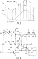
Fig. 3 illustrates a conceptual signal diagram for the bootstrapping technique ofFigs. 2a and 2b ; -
Fig. 4 illustrates an exemplary circuit implementation for the bootstrapping technique ofFigs. 2a and 2b ; -
Fig. 5a illustrates an exemplary implementation of tracking phase A; -
Fig. 5b illustrates an exemplary implementation of tracking phase B; -
Fig. 5c illustrates an exemplary implementation of hold phase C; -
Fig. 6 illustrates an exemplary embodiment of a T/H circuit with a two-phase tracking operation; -
Fig. 7 illustrates an exemplary implementation of the embodiment ofFig. 6 ; -
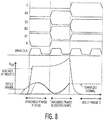
Fig. 8 illustrates an exemplary timing diagram for the embodiment ofFig. 7 ; -
Fig. 9 illustrates another exemplary implementation of the embodiment ofFig. 6 ; and -
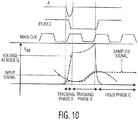
Fig. 10 illustrates an exemplary timing diagram for the embodiment ofFig. 9 . - Referring now to the drawings, in which like numerals refer to like components or steps, there are disclosed broad aspects of various exemplary embodiments.
- According to the foregoing, various exemplary embodiments provide for a system and method for a two-phase tracking operation in an analog-to-digital converter.
- It should be appreciated by those skilled in the art that any block diagrams herein represent conceptual views of illustrative circuitry embodying the principals of the embodiments of the invention.
- A sampling operation of a signal may include two operations, a tracking operation and a hold operation. Circuitry that may perform these operations is called a Track/Hold (T/H) circuit. In an interleaved analog-to-digital converter (ADC) many of these circuits may be multiplexed in time.
- An NMOS switched capacitor implementation of the tracking operation is shown in
Fig. 1a . During the tracking operation the gate terminal of aswitch transistor 102 may be connected to a supply (Vdd) to keep theswitch transistor 102 on and allow the input signal ("IN") to charge asampling capacitor 104. An NMOS switched capacitor implementation of the hold operation is shown inFig. 1b . In the hold operation, the gate terminal of theswitch transistor 102 may be connected to ground to switch off the path between the input signal ("IN") and thesampling capacitor 104. Thesampling capacitor 104 then may store the instantaneous value of the input signal. - A limitation of the T/H implementation shown in
Figs. 1a and 1b may be bandwidth modulation during the tracking operation. The available bandwidth may be partially determined by the on-resistance (Ron) of theswitch transistor 102 and the size of thesampling capacitor 104. The size of thesampling capacitor 104 may be influenced by thermal noise considerations. Thermal noise on capacitors is proportional to kT/C, k being the Boltzman constant, T the temperature, and C the capacitance. - The Ron of the
switch transistor 102 is inversely proportional to Vgs, and linearly proportional to the width/length of theswitch transistor 102. Thus, the modulation of Vgs (where Vgs = Vdd - Vin) may introduce a corresponding modulation to Ron, and thus on the bandwidth, which may translate to signal distortion. The bandwidth modulation may influence the resolution and speed of the ADC. - In order to increase the resolution of the ADC, the size of the
sampling capacitor 104 may be increased. In general, for each extra bit of resolution needed in the ADC, the size of thesampling capacitor 104 may be increased approximately four times to reduce the thermal noise also by 1 bit. However, as previously noted, a larger capacitor may reduce bandwidth. To overcome this reduction in bandwidth, a larger transistor width may be needed to reduce Ron and increase the bandwidth. However, the size of theswitch transistor 102 may also influence the sampled signal. - During the transition from the tracking operation to the hold operation, the charge stored in the NMOS channel of the
switch transistor 102 may be injected from the drain and source, which may alter the sampled signal. This charge is proportional to the width/length dimensions
of theswitch transistor 102. The charge injected from the source of thetransistor 102 is proportional to the value of Vgs at the moment of the transition (Vgs = Vdd - Vin(t), where t = nTs, with Ts being the sampling period and n being the sample number). This charge may create a signal dependent offset and distortion. Similarly, the charge injected from the drain of thetransistor 102 on thesampling capacitor 104 may further distort the sampled signal. - A bootstrapped tracking operation was introduced by A.M. Abo and P.R. Gray in "A 1.5-V, 10-bit, 14.3-MS/s CMOS Pipeline Analog-to-Digital Converter", Journal of Solid State Circuits, vol 34, pp. 599-606. The bootstrapped tracking operation may allow the
switch transistor 102 to be driven with a constant overdrive (typically Vdd), independent of the input signal.Figs. 2a and 2b show a conceptual implementation of the bootstrapping technique. Aswitch 204 is conceptually represented by asingle NMOS transistor 202. In the "OFF" state, the gate of thetransistor 202 may be grounded and theswitch 204 may be open. In the "ON" state, a constant voltage of Vdd maybe applied across the gate and source terminals of thetransistor 202, and theswitch 204 may be closed. A low Ron of thetransistor 202 may be established from the drain to source, independent of the input signal. Although the absolute voltage applied to the gate of thetransistor 202 may exceed Vdd for a positive input signal, none of the relative terminal-to-terminal voltages of thetransistor 202 may exceed Vdd. -
Fig. 3 shows a conceptual signal diagram of a bootstrapped tracking operation. When theswitch 202 is "ON," the voltage at the gate of the transistor 204 ("Vg") may be boosted by Vdd. Therefore, when the switch is "ON", the voltage Vg may be at minimum Vdd, and will vary according to the input signal. - A circuit implementation of a bootstrapped tracking operation is shown in
Fig. 4 . The circuit inFig. 4 may operate on a single phase clock Φ that may turn aswitch transistor 402 on and off. Theswitch transistor 402 performs a switching operation similar to what is shown inFigs. 2a and 2b . During the "OFF" state, Φ is low.Transistors switch transistor 402 to ground. At the same time, Vdd may be applied across abootstrapping capacitor 408 bytransistors bootstrapping capacitor 408 may act as a power source across the gate and source of theswitch transistor 402 during the "ON" state.Transistors switch transistor 402 from thebootstrapping capacitor 408 while it is charging. When Φ goes high, triggering the "ON" state,transistors transistor 414, allowing charge from thebootstrapping capacitor 408 to flow onto the gate of theswitch transistor 402. This may turn on bothtransistor 416 and theswitch transistor 402.Transistor 416 may enable the gate of theswitch transistor 402 to track the input signal ("IN") shifted by Vdd, keeping the gate-source voltage of theswitch transistor 402 substantially constant regardless of the input signal. For example, if the input signal is Vdd, then the gate of theswitch transistor 402 would be 2Vdd. At the same time, the Vgs voltage of theswitch transistor 402 would be Vdd, which may enhance the reliability of theswitch transistor 402, as the difference between the gate and source terminals would not exceed Vdd. -
Transistor 404 may reduce the Vgs and Vgd voltages experienced bytransistor 406 when Φ is low.Transistor 420 may ensure that the Vgs oftransistor 414 does not exceed Vdd. Transistor 422,transistor 424,capacitor 426, capacitor 428, andinverter 430 form a clock multiplier that may enabletransistor 410 to uni-directionally charge thebootstrapping capacitor 408 during the "OFF" state. - Sampling rates in the giga-sample per second (GS/s) range with wide bandwidth, high linearity, and low noise may be difficult to apply to the bootstrapped tracking circuit shown in
Fig. 4 for the following various reasons. - The transition from "OFF" to "ON" of the
switch transistor 402 may be realized by a charge re-distribution between the charge stored at the top-plate of thebootstrapping capacitor 408 and parasitic capacitance at node G. Alarge bootstrapping capacitor 408 and alarge transistor 414 may be necessary to provide a very low ohmic path between node G and thebootstrapping capacitor 408, otherwise the transition of theswitch transistor 402 from "OFF" to "ON" may not occur quickly enough to properly sample the input signal. A slow transition may substantially limit the tracking capability of the T/H circuit. - Ideally the gate of the
switch transistor 402 would be charged to at least Vdd, but due to the large parasitic capacitance present at node G, it may actually be charged to a smaller value. This may translate to a loss of efficiency for theswitch transistor 402. Charge sharing between the top-plate of thebootstrapping capacitor 408 and the parasitic capacitance at node G also may reduce the boosted voltage during the bootstrapped tracking operation. - The bootstrapped tracking operation may be partially enabled by
transistor 416, and may occur only after the voltage at the gate of theswitch transistor 402 has reached a necessary level. This may delay the time for the bootstrapping to become effective, and may reduce the available tracking time. - A
large bootstrapping capacitor 408 may be required for effective bootstrapping and for a quick "OFF" to "ON" transition. However, at high sampling rates thebootstrapping capacitor 408 may need to be re-charged very quickly, which means the transistors connected to it (e.g. transistors
Large transistors may introduce additional parasitic capacitances. Thebootstrapping capacitor 408 may also introduce a large parasitic capacitance to ground due to its size. All these parasitic capacitors may increase the charge sharing effect even further, lowering the charge seen at node G of theswitch transistor 402. - The
large bootstrapping capacitor 408 and large transistors may also introduce significant parasitic capacitance at the input node ("IN"). This may translate to large disturbances at the input node that take time to settle. This may limit the sampling rate of the ADC. The parasitic capacitances of thebootstrapping capacitor 408 and the large transistors may also create a signal delay. - The bootstrapped tracking circuit shown in
Fig. 4 may occupy a large silicon area. When many time-interleaved T/H circuits are used to achieve higher sampling rates, the bootstrapped tracking circuitry may cause each T/H circuit to be further away from each other. This may increase the clock and signal distribution interconnect lengths, further limiting bandwidth and creating negative impact on the timing accuracy of each switching transistor. - Embodiments of the invention described herein decrease the impact of parasitic capacitors significantly, and for this reason improve on all aspects mentioned in the previous paragraphs.
- A conceptual schematic of an embodiment of the present invention is shown in
Figs. 5a, 5b, and 5c , and will be further explained in the following paragraphs.
Embodiments of the present invention may eliminate the need to use the charge stored in a bootstrapping capacitor to quickly charge a switch transistor gate node to Vdd. Therefore, the bootstrapping capacitor may be substantially smaller, improving significantly the performance of the tracking operation, compared to the operation described inFigs. 2 ,3, and 4 . - The tracking operation may be divided into two phases as shown in
Figs. 5a and 5b . In tracking phase A, as shown inFig. 5a , the gate of theswitch transistor 502 may be charged directly to Vdd, as it is done with non-bootstrapped switch transistors (e.g.,Fig. 1a ). This may charge theparasitic capacitor 504 present at node G to Vdd quickly, and may maximize the instantaneous bandwidth available (Vgs = Vg(t) - Vin, where t is the moment node G is switched from ground (or Vss) to Vdd). This may allow for fast recovery from a previous sample stored in asampling capacitor 506. Also during tracking phase A, abootstrap capacitor 508 may be charged by Vdd. - In tracking phase B, as shown in
Fig. 5b , abootstrap capacitor 508 may be operated similarly to the bootstrapped tracking operation shown inFigs. 2 and4 . A fast rising edge of the voltage at the gate of theswitch transistor 502 may trigger the start of tracking phase B, similar to the circuit inFig. 4 . Alternatively, phases A and B may be triggered independently from each other with corresponding control signals. - In phase B, no charge may need to be used from the
bootstrap capacitor 508 as a result of the separate charging path to Vdd that took place in phase A. Thebootstrap capacitor 508 may only be required to enable theswitch transistor 502 to track the input signal ("IN"). - Charge losses due to the
parasitic capacitor 504 in the initial portion of the tracking operation may be significantly reduced, and the bootstrapping voltage may start from at least Vdd. This may allow for asmaller bootstrapping capacitor 508 as compared to thebootstrapping capacitor 408 ofFig. 4 , as well as smaller transistors connected to the bootstrapping capacitor, as shown later inFigs.7 and9 . A significant positive impact on bandwidth, sampling rate, and linearity may be achieved by the two-phase bootstrapping operation compared to the bootstrapping operation ofFigs. 2 and4 . - The capacitive voltage division between the
parasitic capacitor 504 and thebootstrapping capacitor 508 during phase B may remain. However, thebootstrapping capacitor 508 may not need to charge theparasitic capacitor 504 from ground to Vdd before it enables the bootstrapping operation, resulting in a significant reduction of the parasitic capacitance. As a result, if thebootstrapping capacitor 408 ofFig. 4 and thebootstrapping capacitor 508 were the same value, the voltage division due to parasitic capacitances may be significantly smaller with thebootstrapping capacitor 508. - After tracking phases A and B, the circuit may enter hold phase C, as shown in
Fig. 5c . The node G may be connected to Vss or ground, to switch off the path between the input signal and thesampling capacitor 506. Thesampling capacitor 506 then stores the instantaneous value of the input signal. Thebootstrap capacitor 508 may also be charged by Vdd during hold phase C. - An embodiment of a T/H circuit including a two-phase tracking operation is shown in
Fig. 6 . Trackingphase A circuitry 603 may includetransistor 604.Transistor 604 may provide a path to Vdd for the gate ofswitch transistor 602 during tracking phase A. In tracking phase B,transistor 604 may be turned off, and trackingphase B circuitry 606 may enable a bootstrapped tracking operation. In hold phase C, the gate of theswitch transistor 602 may be connected to ground viatransistors sampling capacitor 612. Theswitch transistor 602 andsampling capacitor 612form sampling circuitry 601, similar to the T/H implementation ofFigs. 1a and 1b . Atiming generator 614 may supply control signals to nodes A, B, and C to define the scheduling of the three phases. Thetiming generator 614 may generate the control signals based on amain clock 616 of the ADC. -
Fig. 7 is an example implementation of the embodiment of the T/H circuit ofFig. 6 . As inFig. 6 , trackingphase A circuitry 703 may includetransistor 704.Transistor 704 may provide a path to Vdd for the gate ofswitch transistor 702 during tracking phase A. In tracking phase B,transistor 704 may be turned off, and trackingphase B circuitry 705 may enable a bootstrapped tracking operation. The trackingphase B circuitry 705 may includetransistors bootstrapping capacitor 714.Transistors capacitor 714 to be charged by Vdd. Transistors 706 and 712 may provide path for thebootstrapping capacitor 714 to the gate and source ofswitch transistor 702. In hold phase C, the gate of theswitch transistor 702 may be connected to ground viatransistors sampling capacitor 720. Theswitch transistor 702 andsampling capacitor 720form sampling circuitry 701, similar to the T/H implementation ofFigs. 1a and 1b . Atiming generator 722 may supply control signals to nodes A, B1, B2, B3, B4, and C to define the scheduling of the three phases. Thetiming generator 722 may generate the control signals based on amain clock 724 of the ADC. - The transistors in the tracking
phase B circuitry 705 may be controlled with independent timing signals to reduce loading at node G and to create less parasitic capacitance and a faster pull-down for the hold phase C. - The example implementation in
Fig. 7 may allow thebootstrap capacitor 714 to have more time to charge to Vdd. This may enable the use of asmaller transistor 704 for further reduction of parasitic capacitance, and may improve the capacitor divider effect in the tracking phase B. - Tracking phases A and B may be defined by the
main clock 724 and have a fixed duration, for example one period of the main clock of the ADC, as shown inFig. 8 . -
Transistors -
Fig. 8 shows an exemplary timing diagram for the embodiment ofFig. 7 . In this example, tracking phases A and B may last for one period of the main clock each, and the hold phase C may last for two periods. The timing of phases A, B, and C may be modified to be shorter and/or longer. In tracking phase A, the voltage at node G may be charged to Vdd, independently of the input signal. In tracking phase B, the voltage at node G may remain boosted by Vdd and also may track with the input signal. In hold phase C, the voltage at node G may drop to ground, and the sampled signal may hold its value substantially constant for a period of time to be sampled. - Tracking phase A may be triggered when control signal A is low, control signal B1 is high, control signal B2 is low, control signal B3 is high, control signal B4 is low, and control signal C is low. Tracking phase B may be triggered when control signal A is high, control signal B1 is low, control signal B2 is high, control signal B3 is low, control signal B4 is high, and control signal C is low. Hold phase C may be triggered when control signal A is high, control signal B1 is high, control signal B2 is low, control signal B3 is high, control signal B4 is low, and control signal C is high.
- The control signals shown in
Fig. 8 are examples of the logical (i.e. high/low) waveforms used to define the scheduling of the three phases. The actual signals supplied to the gates oftransistors - Another embodiment illustrating another example implementation is shown in
Fig. 9 . Similar to the implementation shown inFig. 7 , trackingphase A circuitry 903 may includetransistor 904.Transistor 904 may provide a path to Vdd for the gate ofswitch transistor 902 during tracking phase A. In tracking phase B,transistor 902 may be turned off, and trackingphase B circuitry 905 may enable a bootstrapped tracking operation. The trackingphase B circuitry 905 may includetransistors bootstrapping capacitor 914. In hold phase C, the gate of theswitch transistor 902 may be connected to ground viatransistors sampling capacitor 920. Theswitch transistor 902 andsampling capacitor 920form sampling circuitry 901, similar to the T/H implementation ofFigs. 1a and 1b . Atiming generator 922 may supply control signals to nodes A, B1, B2, and C to define the scheduling of the three phases. Thetiming generator 922 may generate the control signals based on amain clock 924 of the ADC. In this implementation,transistors Transistors -
Fig. 10 shows an exemplary timing diagram for the embodiment ofFig. 9 . In this example, tracking phases A and B may occur during the same clock cycle, with tracking phase A lasting only long enough to charge node G to Vdd and tracking phase B starting with a precharged node G. In hold phase C, the voltage at node G may drop to ground, and the sampled signal may hold its value substantially constant for a period of time to be sampled. - Control signals B1, B2, and C may use the same logical waveform. Tracking phase A may be triggered when control signal A is low and control signals B1, B2, and C are high. Tracking phase B may be triggered when control signal A is high and control signals B1, B2, and C are low. Hold phase C may be triggered when control signals A, B1, B2, and C are high.
- The control signals shown in
Fig. 10 are examples of the logical (i.e. high/low) signals used to define the scheduling of the three phases. The actual signals supplied to the gates oftransistors - The pre-charge path is not limited to the implementations shown in the previous examples, and the bootstrap path is not limited to the implementations using capacitors (passive bootstrapping), but may also be implemented with active bootstrapping. With active bootstrapping, the tracking phase B circuitry shown in
Fig. 6 may be a buffer circuit, which may supply a replica version of the input signal with a corresponding voltage offset, e.g., Vdd. A two-phase tracking operation with active bootstrapping may substantially reduce the slew rate requirements of the buffer circuit, which may translate to major power savings and increased speed. - The two-phase tracking operation may allow for various benefits. The operation may allow a high sampling rate for high resolution ADC's because the tracking edge may be well defined, and not modulated by the input signal as in a non-bootstrapped tracking operation. The circuitry may occupy a significantly smaller area, consuming less dynamic power and causing less supply disturbances while providing larger signal bandwidth, as compared to a conventional bootstrapping circuitry. The circuitry may also be used in massively interleaved ADC's due to its small size and low power operation. Because the sampling switches may be located much closer to each other, the size of the clock network also may become smaller with benefits in timing accuracy. The circuitry may enable easier use of bootstrapping in sampling switches and analog multiplexers in an ADC.
- The two-phase tracking circuitry may further enable significantly higher sampling rates for the ADC because the bootstrap capacitor may be very small and thus may be charged faster compared to a conventional bootstrapping circuitry. Sampling rates of several GS/s with a resolution of 10 bits may be possible with these embodiments. The circuitry may reduce the tracking time needed because the gate of the switch transistor may be pulled to Vdd much faster than conventional bootstrapping circuitry. The circuitry may also enable steeper hold transitions, which may result in higher linearity and timing accuracy.
- A T/H circuit with a two-phase tracking operation may be used in a variety of applications, such as, for example, radar applications, high speed wireless communications, cellular communications, satellite communications, cable receivers, satellite receivers, radio astronomy applications, or other applications that may utilize several GS/s sampling rates.
- Although the various exemplary embodiments have been described in detail with particular reference to certain exemplary aspects thereof, it should be understood that the invention is capable of other embodiments and its details are capable of modifications in various obvious respects. Accordingly, the foregoing disclosure, description, and figures are for illustrative purposes only and do not in any way limit the invention, which is defined only by the claims.
Claims (12)
- A tracking system for an analog to digital converter, the tracking system comprising:a transistor switch (602) having a gate node, a source node coupled to an input signal (IN) and a drain node coupled to a sampling capacitor (612);a power source circuit (603) connected to the gate node; anda bootstrapping circuit (606) connected to the source node and to the gate node, the bootstrapping circuit comprising a capacitor (714);wherein the power source circuit is configured to turn on the transistor switch by charging the gate node of the transistor switch during a first tracking phase; andthe bootstrapping circuit is configured to charge the gate node of the transistor switch during a second tracking phase;wherein the first and the second tracking phases are triggered by control signals from a timing generator (614).
- The tracking system of claim 1, wherein a voltage between the gate node and the source node is dependent on the input signal during the first tracking phase.
- The tracking system of claim 1, wherein a voltage between the gate node and the source node is constant during the second tracking phase.
- The tracking system of any preceding claim, wherein the power source circuit charges a parasitic capacitance.
- The tracking system of any preceding claim, wherein the timing generator generates the control signals based on a main clock of the tracking system.
- The tracking system of claim 5, wherein the first tracking phase occurs during a first clock cycle of the main clock and the second tracking phase occurs during a second clock cycle of the main clock.
- The tracking system of claim 5, wherein the first and second tracking phases both occur during a clock cycle of the main clock.
- An analog to digital converter comprising the tracking system of any preceding claim.
- A method for performing a tracking operation on an input signal (IN), comprising:turning on a transistor switch (602) having a gate node (G), sampling capacitor a source node coupled to the input signal (IN) and a drain node coupled to a sampling capacitor (612), by charging the gate node (G) of the transistor switch with a power source circuit (603) during a first tracking phase, the power source circuit being connected to the gate node; andkeeping the transistor switch on by charging the transistor switch gate node with a bootstrapping circuit (606) comprising a capacitor (714) during a second tracking phase, the bootstrapping circuit being connected to the gate node and the source node of the transistor switch,wherein the first and the second tracking phases are triggered by control signals from a timing generator (614).
- The method of claim 9, wherein a voltage between the gate node and the source node is dependent on the input signal during the first tracking phase.
- The method of claim 9, wherein a voltage between the gate node and the source node is constant during the second tracking phase.
- The method of any of claims 9 to 11, wherein the power source circuit charges a parasitic capacitance.
Applications Claiming Priority (1)
| Application Number | Priority Date | Filing Date | Title |
|---|---|---|---|
| US13/094,978 US8664979B2 (en) | 2011-04-27 | 2011-04-27 | Track and hold circuit using a bootstrapping circuit |
Publications (2)
| Publication Number | Publication Date |
|---|---|
| EP2518730A1 EP2518730A1 (en) | 2012-10-31 |
| EP2518730B1 true EP2518730B1 (en) | 2019-08-14 |
Family
ID=46049208
Family Applications (1)
| Application Number | Title | Priority Date | Filing Date |
|---|---|---|---|
| EP12165304.2A Active EP2518730B1 (en) | 2011-04-27 | 2012-04-24 | Tracking and hold operations for an analog-to-digital converter |
Country Status (3)
| Country | Link |
|---|---|
| US (1) | US8664979B2 (en) |
| EP (1) | EP2518730B1 (en) |
| CN (1) | CN102761337B (en) |
Families Citing this family (21)
| Publication number | Priority date | Publication date | Assignee | Title |
|---|---|---|---|---|
| US8525574B1 (en) * | 2012-05-15 | 2013-09-03 | Lsi Corporation | Bootstrap switch circuit with over-voltage prevention |
| US8536928B1 (en) * | 2012-05-25 | 2013-09-17 | Fairchild Semiconductor Corporation | Constant VGS charge pump for load switch applications |
| US8981843B2 (en) * | 2012-05-31 | 2015-03-17 | Fairchild Semiconductor Corporation | Translator including overstress protection |
| US8975923B2 (en) * | 2012-08-20 | 2015-03-10 | Fairchild Semiconductor Corporation | Protective multiplexer |
| US8866652B2 (en) | 2013-03-07 | 2014-10-21 | Analog Devices, Inc. | Apparatus and method for reducing sampling circuit timing mismatch |
| DE102014222651B4 (en) * | 2014-11-06 | 2022-09-29 | Infineon Technologies Ag | Circuit chip for implementing a digital sensor system |
| KR20160114538A (en) | 2015-03-24 | 2016-10-05 | 페어차일드 세미컨덕터 코포레이션 | Enhanced protective multiplexer |
| US9419639B1 (en) | 2015-09-23 | 2016-08-16 | Qualcomm Incorporated | Low distortion sample and hold switch |
| US9484905B1 (en) | 2016-01-22 | 2016-11-01 | Freescale Semiconductor, Inc. | Voltage sampling switch and method therefor |
| US9893738B2 (en) | 2016-05-11 | 2018-02-13 | Samsung Electronics Co., Ltd. | Analog-to-digital converter and communication device including the same |
| US10727828B2 (en) * | 2016-09-12 | 2020-07-28 | Analog Devices, Inc. | Input buffer |
| TWI849512B (en) * | 2016-09-12 | 2024-07-21 | 美商美國亞德諾半導體公司 | Bootstrapped switching circuit |
| US10295572B1 (en) | 2018-04-12 | 2019-05-21 | Nxp Usa, Inc. | Voltage sampling switch |
| US10790817B2 (en) * | 2019-02-08 | 2020-09-29 | Qorvo Us, Inc. | Power switch with bootstrap driver for continuous time operation |
| US11322217B2 (en) * | 2019-08-27 | 2022-05-03 | Texas Instruments Incorporated | Track and hold circuits with transformer coupled bootstrap switch |
| US10897263B1 (en) * | 2020-05-14 | 2021-01-19 | Telefonaktiebolaget Lm Ericsson (Publ) | Multiple paths bootstrap configuration for sample and hold circuit |
| US11533050B1 (en) | 2021-06-25 | 2022-12-20 | Nxp Usa, Inc. | Differential bootstrapped track-and-hold circuit with cross-coupled dummy sampling switches |
| US11804836B1 (en) * | 2022-05-20 | 2023-10-31 | Analog Devices, Inc. | Bootstrapped switch with fast turn off |
| CN119892091B (en) * | 2025-03-31 | 2025-07-08 | 湖南融创微电子股份有限公司 | Transmission gate switch sampling circuit with substrate bias |
| CN121150671A (en) * | 2025-11-18 | 2025-12-16 | 共模半导体技术(苏州)有限公司 | A bootstrap switching circuit with high response speed |
| CN121461996B (en) * | 2026-01-05 | 2026-04-03 | 成都纳川微电子科技有限公司 | Bootstrap sampling switch circuit with precharge and analog-to-digital converter |
Family Cites Families (9)
| Publication number | Priority date | Publication date | Assignee | Title |
|---|---|---|---|---|
| US6072355A (en) * | 1998-01-22 | 2000-06-06 | Burr-Brown Corporation | Bootstrapped CMOS sample and hold circuitry and method |
| US6265911B1 (en) * | 1999-12-02 | 2001-07-24 | Analog Devices, Inc. | Sample and hold circuit having improved linearity |
| US6972706B2 (en) * | 2001-08-10 | 2005-12-06 | Walter Jan Maria Snoeijs | Current folding cell and circuit comprising at least one folding cell |
| US6525574B1 (en) * | 2001-09-06 | 2003-02-25 | Texas Instruments Incorporated | Gate bootstrapped CMOS sample-and-hold circuit |
| US7218154B1 (en) * | 2005-03-31 | 2007-05-15 | Ami Semiconductor, Inc. | Track and hold circuit with operating point sensitive current mode based offset compensation |
| US7397284B1 (en) * | 2007-04-03 | 2008-07-08 | Xilinx, Inc. | Bootstrapped circuit |
| JP4505027B2 (en) * | 2008-05-08 | 2010-07-14 | 株式会社半導体理工学研究センター | Sample hold circuit and A / D converter |
| CN101645710B (en) * | 2009-09-03 | 2012-07-04 | 复旦大学 | Low supply voltage pipelined folded interpolating analog-to-digital converter |
| CN101977059A (en) * | 2010-11-23 | 2011-02-16 | 复旦大学 | Sample-and-hold circuit at front end of superhigh speed flash analog-digital converter |
-
2011
- 2011-04-27 US US13/094,978 patent/US8664979B2/en active Active
-
2012
- 2012-04-24 EP EP12165304.2A patent/EP2518730B1/en active Active
- 2012-04-24 CN CN201210122635.XA patent/CN102761337B/en active Active
Non-Patent Citations (1)
| Title |
|---|
| None * |
Also Published As
| Publication number | Publication date |
|---|---|
| US8664979B2 (en) | 2014-03-04 |
| CN102761337A (en) | 2012-10-31 |
| CN102761337B (en) | 2015-08-05 |
| EP2518730A1 (en) | 2012-10-31 |
| US20120274362A1 (en) | 2012-11-01 |
Similar Documents
| Publication | Publication Date | Title |
|---|---|---|
| US8664979B2 (en) | Track and hold circuit using a bootstrapping circuit | |
| JP6938538B2 (en) | Time-interleaved sequential comparison Asynchronous clock generation for analog-to-digital converters | |
| EP2719078B1 (en) | Distributed bootstrap switch | |
| US8610422B2 (en) | Dynamic biasing of an amplifier using capacitive driving of internal bias voltages | |
| KR20050111526A (en) | Sampling switch | |
| US20190190505A1 (en) | Delay control circuits | |
| US8830095B2 (en) | Track and hold circuit and method | |
| US10148277B1 (en) | Current steering digital to analog converter with decoder free quad switching | |
| US8294512B2 (en) | Bootstrapped clock generator and track-and-hold circuit including the same | |
| EP3342045B1 (en) | Shared circuit configurations for bootstrapped sample and hold circuits in a time-interleaved analog to digital converter | |
| US11689200B2 (en) | Sampling switch circuits | |
| CN105897264B (en) | Fast turn-off/on source follower | |
| US20170222639A1 (en) | Electronic Switching Device with Reduction of Leakage Currents and Corresponding Control Method | |
| Ramkaj et al. | Fast switch bootstrapping for GS/s high-resolution analog-to-digital converter | |
| US8232904B2 (en) | Folding analog-to-digital converter | |
| Huang et al. | A fast bootstrapped switch for high-speed high-resolution A/D converter | |
| KR102435395B1 (en) | Sampling switch for high dynamic input range and method for operating the same | |
| CN114696810B (en) | A gate bootstrap switch circuit and control method thereof | |
| CN110599939B (en) | Gate driving unit and gate driving method | |
| US7635996B2 (en) | Differential blocking sampler, in particular for an analog digital converter | |
| US20260066898A1 (en) | Device and method for switch control | |
| CN113206659B (en) | High-speed high-linearity grid voltage bootstrap switch for pipeline ADC | |
| CN112823474A (en) | CMOS transistor, circuit for driving liquid crystal pixel and CMOS transmission gate | |
| US10014876B1 (en) | High speed buffering for time-interleaved ADCS with reduced ISI and increased voltage gain | |
| CN121984488A (en) | A gate voltage bootstrap switch |
Legal Events
| Date | Code | Title | Description |
|---|---|---|---|
| PUAI | Public reference made under article 153(3) epc to a published international application that has entered the european phase |
Free format text: ORIGINAL CODE: 0009012 |
|
| AK | Designated contracting states |
Kind code of ref document: A1 Designated state(s): AL AT BE BG CH CY CZ DE DK EE ES FI FR GB GR HR HU IE IS IT LI LT LU LV MC MK MT NL NO PL PT RO RS SE SI SK SM TR |
|
| AX | Request for extension of the european patent |
Extension state: BA ME |
|
| 17P | Request for examination filed |
Effective date: 20130502 |
|
| STAA | Information on the status of an ep patent application or granted ep patent |
Free format text: STATUS: EXAMINATION IS IN PROGRESS |
|
| 17Q | First examination report despatched |
Effective date: 20171002 |
|
| GRAP | Despatch of communication of intention to grant a patent |
Free format text: ORIGINAL CODE: EPIDOSNIGR1 |
|
| STAA | Information on the status of an ep patent application or granted ep patent |
Free format text: STATUS: GRANT OF PATENT IS INTENDED |
|
| INTG | Intention to grant announced |
Effective date: 20190410 |
|
| GRAJ | Information related to disapproval of communication of intention to grant by the applicant or resumption of examination proceedings by the epo deleted |
Free format text: ORIGINAL CODE: EPIDOSDIGR1 |
|
| STAA | Information on the status of an ep patent application or granted ep patent |
Free format text: STATUS: EXAMINATION IS IN PROGRESS |
|
| GRAP | Despatch of communication of intention to grant a patent |
Free format text: ORIGINAL CODE: EPIDOSNIGR1 |
|
| STAA | Information on the status of an ep patent application or granted ep patent |
Free format text: STATUS: GRANT OF PATENT IS INTENDED |
|
| GRAS | Grant fee paid |
Free format text: ORIGINAL CODE: EPIDOSNIGR3 |
|
| GRAA | (expected) grant |
Free format text: ORIGINAL CODE: 0009210 |
|
| STAA | Information on the status of an ep patent application or granted ep patent |
Free format text: STATUS: THE PATENT HAS BEEN GRANTED |
|
| INTC | Intention to grant announced (deleted) | ||
| INTG | Intention to grant announced |
Effective date: 20190702 |
|
| AK | Designated contracting states |
Kind code of ref document: B1 Designated state(s): AL AT BE BG CH CY CZ DE DK EE ES FI FR GB GR HR HU IE IS IT LI LT LU LV MC MK MT NL NO PL PT RO RS SE SI SK SM TR |
|
| REG | Reference to a national code |
Ref country code: GB Ref legal event code: FG4D |
|
| REG | Reference to a national code |
Ref country code: CH Ref legal event code: EP Ref country code: AT Ref legal event code: REF Ref document number: 1167985 Country of ref document: AT Kind code of ref document: T Effective date: 20190815 |
|
| REG | Reference to a national code |
Ref country code: DE Ref legal event code: R096 Ref document number: 602012062887 Country of ref document: DE |
|
| REG | Reference to a national code |
Ref country code: IE Ref legal event code: FG4D |
|
| REG | Reference to a national code |
Ref country code: NL Ref legal event code: MP Effective date: 20190814 |
|
| REG | Reference to a national code |
Ref country code: LT Ref legal event code: MG4D |
|
| PG25 | Lapsed in a contracting state [announced via postgrant information from national office to epo] |
Ref country code: BG Free format text: LAPSE BECAUSE OF FAILURE TO SUBMIT A TRANSLATION OF THE DESCRIPTION OR TO PAY THE FEE WITHIN THE PRESCRIBED TIME-LIMIT Effective date: 20191114 Ref country code: SE Free format text: LAPSE BECAUSE OF FAILURE TO SUBMIT A TRANSLATION OF THE DESCRIPTION OR TO PAY THE FEE WITHIN THE PRESCRIBED TIME-LIMIT Effective date: 20190814 Ref country code: NO Free format text: LAPSE BECAUSE OF FAILURE TO SUBMIT A TRANSLATION OF THE DESCRIPTION OR TO PAY THE FEE WITHIN THE PRESCRIBED TIME-LIMIT Effective date: 20191114 Ref country code: NL Free format text: LAPSE BECAUSE OF FAILURE TO SUBMIT A TRANSLATION OF THE DESCRIPTION OR TO PAY THE FEE WITHIN THE PRESCRIBED TIME-LIMIT Effective date: 20190814 Ref country code: PT Free format text: LAPSE BECAUSE OF FAILURE TO SUBMIT A TRANSLATION OF THE DESCRIPTION OR TO PAY THE FEE WITHIN THE PRESCRIBED TIME-LIMIT Effective date: 20191216 Ref country code: HR Free format text: LAPSE BECAUSE OF FAILURE TO SUBMIT A TRANSLATION OF THE DESCRIPTION OR TO PAY THE FEE WITHIN THE PRESCRIBED TIME-LIMIT Effective date: 20190814 Ref country code: FI Free format text: LAPSE BECAUSE OF FAILURE TO SUBMIT A TRANSLATION OF THE DESCRIPTION OR TO PAY THE FEE WITHIN THE PRESCRIBED TIME-LIMIT Effective date: 20190814 Ref country code: LT Free format text: LAPSE BECAUSE OF FAILURE TO SUBMIT A TRANSLATION OF THE DESCRIPTION OR TO PAY THE FEE WITHIN THE PRESCRIBED TIME-LIMIT Effective date: 20190814 |
|
| REG | Reference to a national code |
Ref country code: AT Ref legal event code: MK05 Ref document number: 1167985 Country of ref document: AT Kind code of ref document: T Effective date: 20190814 |
|
| PG25 | Lapsed in a contracting state [announced via postgrant information from national office to epo] |
Ref country code: GR Free format text: LAPSE BECAUSE OF FAILURE TO SUBMIT A TRANSLATION OF THE DESCRIPTION OR TO PAY THE FEE WITHIN THE PRESCRIBED TIME-LIMIT Effective date: 20191115 Ref country code: LV Free format text: LAPSE BECAUSE OF FAILURE TO SUBMIT A TRANSLATION OF THE DESCRIPTION OR TO PAY THE FEE WITHIN THE PRESCRIBED TIME-LIMIT Effective date: 20190814 Ref country code: ES Free format text: LAPSE BECAUSE OF FAILURE TO SUBMIT A TRANSLATION OF THE DESCRIPTION OR TO PAY THE FEE WITHIN THE PRESCRIBED TIME-LIMIT Effective date: 20190814 Ref country code: AL Free format text: LAPSE BECAUSE OF FAILURE TO SUBMIT A TRANSLATION OF THE DESCRIPTION OR TO PAY THE FEE WITHIN THE PRESCRIBED TIME-LIMIT Effective date: 20190814 Ref country code: RS Free format text: LAPSE BECAUSE OF FAILURE TO SUBMIT A TRANSLATION OF THE DESCRIPTION OR TO PAY THE FEE WITHIN THE PRESCRIBED TIME-LIMIT Effective date: 20190814 Ref country code: IS Free format text: LAPSE BECAUSE OF FAILURE TO SUBMIT A TRANSLATION OF THE DESCRIPTION OR TO PAY THE FEE WITHIN THE PRESCRIBED TIME-LIMIT Effective date: 20191214 |
|
| PG25 | Lapsed in a contracting state [announced via postgrant information from national office to epo] |
Ref country code: TR Free format text: LAPSE BECAUSE OF FAILURE TO SUBMIT A TRANSLATION OF THE DESCRIPTION OR TO PAY THE FEE WITHIN THE PRESCRIBED TIME-LIMIT Effective date: 20190814 |
|
| PG25 | Lapsed in a contracting state [announced via postgrant information from national office to epo] |
Ref country code: PL Free format text: LAPSE BECAUSE OF FAILURE TO SUBMIT A TRANSLATION OF THE DESCRIPTION OR TO PAY THE FEE WITHIN THE PRESCRIBED TIME-LIMIT Effective date: 20190814 Ref country code: RO Free format text: LAPSE BECAUSE OF FAILURE TO SUBMIT A TRANSLATION OF THE DESCRIPTION OR TO PAY THE FEE WITHIN THE PRESCRIBED TIME-LIMIT Effective date: 20190814 Ref country code: EE Free format text: LAPSE BECAUSE OF FAILURE TO SUBMIT A TRANSLATION OF THE DESCRIPTION OR TO PAY THE FEE WITHIN THE PRESCRIBED TIME-LIMIT Effective date: 20190814 Ref country code: AT Free format text: LAPSE BECAUSE OF FAILURE TO SUBMIT A TRANSLATION OF THE DESCRIPTION OR TO PAY THE FEE WITHIN THE PRESCRIBED TIME-LIMIT Effective date: 20190814 Ref country code: DK Free format text: LAPSE BECAUSE OF FAILURE TO SUBMIT A TRANSLATION OF THE DESCRIPTION OR TO PAY THE FEE WITHIN THE PRESCRIBED TIME-LIMIT Effective date: 20190814 Ref country code: IT Free format text: LAPSE BECAUSE OF FAILURE TO SUBMIT A TRANSLATION OF THE DESCRIPTION OR TO PAY THE FEE WITHIN THE PRESCRIBED TIME-LIMIT Effective date: 20190814 |
|
| PG25 | Lapsed in a contracting state [announced via postgrant information from national office to epo] |
Ref country code: IS Free format text: LAPSE BECAUSE OF FAILURE TO SUBMIT A TRANSLATION OF THE DESCRIPTION OR TO PAY THE FEE WITHIN THE PRESCRIBED TIME-LIMIT Effective date: 20200224 Ref country code: SM Free format text: LAPSE BECAUSE OF FAILURE TO SUBMIT A TRANSLATION OF THE DESCRIPTION OR TO PAY THE FEE WITHIN THE PRESCRIBED TIME-LIMIT Effective date: 20190814 Ref country code: CZ Free format text: LAPSE BECAUSE OF FAILURE TO SUBMIT A TRANSLATION OF THE DESCRIPTION OR TO PAY THE FEE WITHIN THE PRESCRIBED TIME-LIMIT Effective date: 20190814 Ref country code: SK Free format text: LAPSE BECAUSE OF FAILURE TO SUBMIT A TRANSLATION OF THE DESCRIPTION OR TO PAY THE FEE WITHIN THE PRESCRIBED TIME-LIMIT Effective date: 20190814 |
|
| REG | Reference to a national code |
Ref country code: DE Ref legal event code: R097 Ref document number: 602012062887 Country of ref document: DE |
|
| PLBE | No opposition filed within time limit |
Free format text: ORIGINAL CODE: 0009261 |
|
| STAA | Information on the status of an ep patent application or granted ep patent |
Free format text: STATUS: NO OPPOSITION FILED WITHIN TIME LIMIT |
|
| PG2D | Information on lapse in contracting state deleted |
Ref country code: IS |
|
| 26N | No opposition filed |
Effective date: 20200603 |
|
| PG25 | Lapsed in a contracting state [announced via postgrant information from national office to epo] |
Ref country code: SI Free format text: LAPSE BECAUSE OF FAILURE TO SUBMIT A TRANSLATION OF THE DESCRIPTION OR TO PAY THE FEE WITHIN THE PRESCRIBED TIME-LIMIT Effective date: 20190814 |
|
| PG25 | Lapsed in a contracting state [announced via postgrant information from national office to epo] |
Ref country code: MC Free format text: LAPSE BECAUSE OF FAILURE TO SUBMIT A TRANSLATION OF THE DESCRIPTION OR TO PAY THE FEE WITHIN THE PRESCRIBED TIME-LIMIT Effective date: 20190814 |
|
| REG | Reference to a national code |
Ref country code: CH Ref legal event code: PL |
|
| PG25 | Lapsed in a contracting state [announced via postgrant information from national office to epo] |
Ref country code: LI Free format text: LAPSE BECAUSE OF NON-PAYMENT OF DUE FEES Effective date: 20200430 Ref country code: CH Free format text: LAPSE BECAUSE OF NON-PAYMENT OF DUE FEES Effective date: 20200430 Ref country code: FR Free format text: LAPSE BECAUSE OF NON-PAYMENT OF DUE FEES Effective date: 20200430 Ref country code: LU Free format text: LAPSE BECAUSE OF NON-PAYMENT OF DUE FEES Effective date: 20200424 |
|
| REG | Reference to a national code |
Ref country code: BE Ref legal event code: MM Effective date: 20200430 |
|
| PG25 | Lapsed in a contracting state [announced via postgrant information from national office to epo] |
Ref country code: BE Free format text: LAPSE BECAUSE OF NON-PAYMENT OF DUE FEES Effective date: 20200430 |
|
| GBPC | Gb: european patent ceased through non-payment of renewal fee |
Effective date: 20200424 |
|
| PG25 | Lapsed in a contracting state [announced via postgrant information from national office to epo] |
Ref country code: IE Free format text: LAPSE BECAUSE OF NON-PAYMENT OF DUE FEES Effective date: 20200424 Ref country code: GB Free format text: LAPSE BECAUSE OF NON-PAYMENT OF DUE FEES Effective date: 20200424 |
|
| PG25 | Lapsed in a contracting state [announced via postgrant information from national office to epo] |
Ref country code: MT Free format text: LAPSE BECAUSE OF FAILURE TO SUBMIT A TRANSLATION OF THE DESCRIPTION OR TO PAY THE FEE WITHIN THE PRESCRIBED TIME-LIMIT Effective date: 20190814 Ref country code: CY Free format text: LAPSE BECAUSE OF FAILURE TO SUBMIT A TRANSLATION OF THE DESCRIPTION OR TO PAY THE FEE WITHIN THE PRESCRIBED TIME-LIMIT Effective date: 20190814 |
|
| PG25 | Lapsed in a contracting state [announced via postgrant information from national office to epo] |
Ref country code: MK Free format text: LAPSE BECAUSE OF FAILURE TO SUBMIT A TRANSLATION OF THE DESCRIPTION OR TO PAY THE FEE WITHIN THE PRESCRIBED TIME-LIMIT Effective date: 20190814 |
|
| P01 | Opt-out of the competence of the unified patent court (upc) registered |
Effective date: 20230725 |
|
| PGFP | Annual fee paid to national office [announced via postgrant information from national office to epo] |
Ref country code: DE Payment date: 20250319 Year of fee payment: 14 |