EP2506313A1 - Solar cell and method for manufacturing same - Google Patents
Solar cell and method for manufacturing same Download PDFInfo
- Publication number
- EP2506313A1 EP2506313A1 EP11832667A EP11832667A EP2506313A1 EP 2506313 A1 EP2506313 A1 EP 2506313A1 EP 11832667 A EP11832667 A EP 11832667A EP 11832667 A EP11832667 A EP 11832667A EP 2506313 A1 EP2506313 A1 EP 2506313A1
- Authority
- EP
- European Patent Office
- Prior art keywords
- layer
- buffer layer
- solar cell
- light absorbing
- annealing
- Prior art date
- Legal status (The legal status is an assumption and is not a legal conclusion. Google has not performed a legal analysis and makes no representation as to the accuracy of the status listed.)
- Granted
Links
Images


Classifications
-
- H—ELECTRICITY
- H10—SEMICONDUCTOR DEVICES; ELECTRIC SOLID-STATE DEVICES NOT OTHERWISE PROVIDED FOR
- H10F—INORGANIC SEMICONDUCTOR DEVICES SENSITIVE TO INFRARED RADIATION, LIGHT, ELECTROMAGNETIC RADIATION OF SHORTER WAVELENGTH OR CORPUSCULAR RADIATION
- H10F10/00—Individual photovoltaic cells, e.g. solar cells
- H10F10/10—Individual photovoltaic cells, e.g. solar cells having potential barriers
- H10F10/16—Photovoltaic cells having only PN heterojunction potential barriers
- H10F10/167—Photovoltaic cells having only PN heterojunction potential barriers comprising Group I-III-VI materials, e.g. CdS/CuInSe2 [CIS] heterojunction photovoltaic cells
-
- H—ELECTRICITY
- H10—SEMICONDUCTOR DEVICES; ELECTRIC SOLID-STATE DEVICES NOT OTHERWISE PROVIDED FOR
- H10F—INORGANIC SEMICONDUCTOR DEVICES SENSITIVE TO INFRARED RADIATION, LIGHT, ELECTROMAGNETIC RADIATION OF SHORTER WAVELENGTH OR CORPUSCULAR RADIATION
- H10F71/00—Manufacture or treatment of devices covered by this subclass
- H10F71/128—Annealing
-
- Y—GENERAL TAGGING OF NEW TECHNOLOGICAL DEVELOPMENTS; GENERAL TAGGING OF CROSS-SECTIONAL TECHNOLOGIES SPANNING OVER SEVERAL SECTIONS OF THE IPC; TECHNICAL SUBJECTS COVERED BY FORMER USPC CROSS-REFERENCE ART COLLECTIONS [XRACs] AND DIGESTS
- Y02—TECHNOLOGIES OR APPLICATIONS FOR MITIGATION OR ADAPTATION AGAINST CLIMATE CHANGE
- Y02E—REDUCTION OF GREENHOUSE GAS [GHG] EMISSIONS, RELATED TO ENERGY GENERATION, TRANSMISSION OR DISTRIBUTION
- Y02E10/00—Energy generation through renewable energy sources
- Y02E10/50—Photovoltaic [PV] energy
- Y02E10/541—CuInSe2 material PV cells
-
- Y—GENERAL TAGGING OF NEW TECHNOLOGICAL DEVELOPMENTS; GENERAL TAGGING OF CROSS-SECTIONAL TECHNOLOGIES SPANNING OVER SEVERAL SECTIONS OF THE IPC; TECHNICAL SUBJECTS COVERED BY FORMER USPC CROSS-REFERENCE ART COLLECTIONS [XRACs] AND DIGESTS
- Y02—TECHNOLOGIES OR APPLICATIONS FOR MITIGATION OR ADAPTATION AGAINST CLIMATE CHANGE
- Y02P—CLIMATE CHANGE MITIGATION TECHNOLOGIES IN THE PRODUCTION OR PROCESSING OF GOODS
- Y02P70/00—Climate change mitigation technologies in the production process for final industrial or consumer products
- Y02P70/50—Manufacturing or production processes characterised by the final manufactured product
Definitions
- the disclosure relates to a solar cell and a method for manufacturing the same.
- the solar cell is classified into a silicon solar cell, a non-silicon solar cell, and a dye-sensitized solar cell.
- the non-silicon solar cell can be formed by using a thin film, so the non-silicon solar cell can reduce consumption of the material while diversifying the application range of the solar cell.
- a light absorbing layer used in the non-silicon solar cell may be rarely deteriorated by light, so the life span of the non-silicon solar cell may be lengthened.
- the embodiment provides a solar cell capable of improving the photoelectric conversion efficiency and a method of manufacturing the same.
- a method for manufacturing a solar cell includes the steps of forming a first electrode layer on a substrate; forming a light absorbing layer on the first electrode layer; forming a buffer layer on the light absorbing layer; annealing the buffer layer to reduce an oxygen content in the buffer layer; and forming a second electrode layer on the buffer layer.
- the annealing includes a rapid thermal annealing (RTA) and the annealing temperature is in a range of 250°C to 400°C.
- RTA rapid thermal annealing
- the annealing is performed in a vacuum atmosphere or a hydrogen atmosphere.
- the buffer layer has the oxygen content in a range of 2 at% to 5 at% after the annealing.
- the buffer layer has the oxygen content of 6 at% or more before the annealing.
- the buffer layer is formed through a chemical bath deposition (CBD) scheme.
- the buffer layer includes CdS or ZnS.
- a solar cell includes a substrate; a first electrode layer on the substrate; a light absorbing layer on the first electrode layer; a buffer layer formed on the light absorbing layer and having an oxygen content in a range of 2 at% to 5 at%; and a second electrode layer on the buffer layer.
- the buffer layer includes CdS or ZnS.
- the oxygen content in the buffer layer can be adjusted by annealing the buffer layer, so that the recombination at the interfacial surface of the light absorbing layer can be prevented and the photoelectric conversion efficiency can be improved.
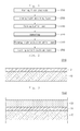
- FIG. 1 is a flowchart showing a method for manufacturing a solar cell according to the embodiment
- FIGS. 2 to 7 are sectional views showing the manufacturing steps of a method for manufacturing a solar cell according to the embodiment.
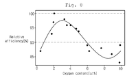
- FIG. 8 is a graph showing a relative efficiency of a solar cell as a function of an oxygen content of a buffer layer.
- the size or the thickness of the layer (film), the region, the pattern or the structure may be modified exaggerated for the purpose of explanation and clarity.
- the size may not utterly reflect the actual size.
- FIG. 1 is a flowchart showing a method for manufacturing a solar cell according to the embodiment
- FIGS. 2 to 7 are sectional views showing the manufacturing steps of the method for manufacturing the solar cell according to the embodiment.
- the method for manufacturing the solar cell may include the steps of forming a first electrode layer ST10, forming a light absorbing layer ST20, forming a buffer layer ST30, performing an annealing process ST40, forming a high-resistance buffer layer ST50, and forming a second electrode layer ST60. These steps will be described in detail with reference to FIGS. 2 to 7 .
- a substrate 10 is prepared and a first electrode layer 31 is formed on the substrate 10 in step ST10.
- the substrate 10 has a plate shape and supports the first electrode layer 31 formed thereon.
- the substrate 10 may include an insulator, such as glass or plastic.
- the substrate 10 may include soda lime glass.
- the embodiment is not limited thereto.
- the substrate 10 may include a metallic substrate. That is, the substrate 10 may be formed by using a rigid material or a flexible material according to the property of the solar cell.
- the first electrode layer 31 may include various conductive materials.
- the first electrode layer 31 may include Mo, Cu, Ni, Al and an alloy thereof.
- the first electrode layer 31 can be formed through various processes. For instance, the first electrode layer 31 can be formed by depositing Mo through the sputtering process.
- the first electrode layer 31 may include at least two layers.
- the layers may be formed by using the homogeneous metal or heterogeneous metals.
- the first electrode layer 31 including at least two layers can be formed by performing the process twice under the different process conditions.
- the first electrode layer 31 is directly formed on the substrate 10, but the embodiment is not limited thereto.
- a diffusion barrier layer (not shown) may be formed between the substrate 10 and the first electrode layer 31.
- a light absorbing layer 33 is formed on the first electrode layer 31 in the step of forming the light absorbing layer ST20.
- the light absorbing layer 33 may include a non-silicon semiconductor material.
- the light absorbing layer 33 may include group I-III-IV compounds.
- the light absorbing layer 33 may include Cu-In-Ga-Se (CIGS) compounds, Cu-In-Se (CIS) compounds, or Cu-Ga-Se (CGS) compounds.
- the light absorbing layer 33 may include group II-IV compounds or III-IV compounds.
- the light absorbing layer 33 may include Cd-Te compounds or Ga-As compounds.
- the light absorbing layer 33 may have an energy bandgap in the range of about 1eV to about 1.8eV. However, the embodiment is not limited thereto, and the light absorbing layer 33 may have various energy bandgaps.
- the light absorbing layer 33 can be formed through various schemes, such as an evaporation scheme or a sputtering scheme.
- the CIGS light absorbing layer 33 is formed by simultaneously or separately evaporating Cu, In, Ga and Se.
- a metallic precursor layer is formed and then the selenization process is performed to form the CIGS light absorbing layer 33. That is, according to the sputtering scheme, the metallic precursor layer including Cu, In and Ga is formed by using a Cu target, an In target and a Ga target. Then, the selenization process is performed to form the CIGS light absorbing layer 33. Otherwise, the sputtering process and the selenization process are simultaneously performed to form the CIGS light absorbing layer 33.
- various types of light absorbing layers 33 can be formed by varying the target and the evaporation material according to the source materials.
- a buffer layer 35a is formed on the light absorbing layer 33 in the steps of forming the buffer layer ST30.
- the buffer layer 35a is provided to attenuate the difference in lattice constant and energy bandgap with respect to a second electrode 29.
- the buffer layer 35a may include CdS or ZnS.
- the buffer layer 35a can be formed through the chemical bath deposition (CBD).
- the buffer layer 35a including CdS can be formed by dipping the light absorbing layer 33 in a solution to form the buffer layer, in which Cd 2+ and S2- are excessively saturated, and then maintaining a predetermined reaction temperature for a predetermined time.
- the solution to form the buffer layer may include cadmium acetate or thiourea.
- a buffering agent or ammonia may be further added in the solution.
- the reaction temperature may be in the range of about 50 to about 100 , but the embodiment is not limited thereto.
- the oxygen content of the buffer layer 35a formed through the above process may be approximate to 6% or more.
- the annealing step ST40 is performed to reduce the oxygen content in the buffer layer 35a, thereby forming a buffer layer 35 having a reduced oxygen content (hereinafter, referred to as "annealed buffer layer".
- the buffer layer 35a is annealed through the rapid thermal annealing (RTA) process to reduce the oxygen content in the buffer layer 35a.
- RTA rapid thermal annealing
- the annealing temperature is in the range of 250 to 400 . If the annealing temperature exceeds 400 , re-deposition and crack may occur so that the buffer layer 35a may be damaged. If the annealing temperature is less than 250 , the oxygen content may be rarely reduced through the annealing process. That is, the annealing temperature is determined in such a manner that the oxygen content in the buffer layer 35a can be property reduce without causing the damage to the buffer layer 35a.
- the annealing step may be performed in the atmosphere suitable for reducing the oxygen content in the buffer layer 35a.
- the annealing step may be performed in the vacuum atmosphere or the hydrogen atmosphere.
- the annealed buffer layer 35 formed through the annealing step ST40 may have the oxygen content in the range of 2 at% to 5 at%.
- a high-resistance buffer layer 37 is formed on the annealed buffer layer 35 in the step of forming the high-resistance buffer layer ST50.
- the high-resistance buffer layer 37 is provided to prevent the buffer layer 35 from being damaged when the second electrode layer 39 is formed.
- the high-resistance buffer layer 37 can be formed by depositing ZnO.
- the embodiment is not limited thereto, but the high-resistance buffer layer 37 can be formed through various schemes by using various materials.
- the high-resistance buffer layer 37 is not an essential element and can be omitted.
- the second electrode layer 39 (or window layer) is formed on the buffer layer, in detail, on the high-resistance buffer layer 37 in the step of forming the second electrode ST60.
- the second electrode layer 39 is transparent so the light can be incident into the second electrode layer 39.
- the second electrode may be formed by using a transmissive conductive material serving as an electrode.
- the second electrode layer 39 has the characteristic of an N type semiconductor, so the second electrode layer 39 may form an N type semiconductor layer together with the buffer layer 35 and may form a PN junction together with the light absorbing layer 33 serving as a P type semiconductor layer.
- the second electrode layer 39 may be formed by using a transparent conductive material, such as aluminum-doped zinc oxide (AZO), fluorine-doped tin oxide (FTO), gallium-doped zinc oxide (GZO), or boron-doped zinc oxide (BZO).
- AZO aluminum-doped zinc oxide
- FTO fluorine-doped tin oxide
- GZO gallium-doped zinc oxide
- BZO boron-doped zinc oxide
- the solar cell manufacture according to the above method may include the substrate 10, the first electrode layer 31, the light absorbing layer 33, the annealed buffer layer 35 and the second electrode layer.
- the high-resistance buffer layer 37 may be disposed between the annealed buffer layer 35 and the second electrode layer 39.
- the annealed buffer layer 35 may include CdS or ZnS and has the oxygen content fin the range of 2 at% to 5 at%.
- the oxygen content in the annealed buffer layer 35 is equal to or less than 5 at%, the photoelectric conversion efficiency of the solar cell can be improved. If the oxygen content in the annealed buffer layer 35 exceeds 5 at%, oxygen in the annealed buffer layer 35 may serve as an electron trap, lowering the photoelectric conversion efficiency. Thus, according to the embodiment, the oxygen content in the annealed buffer layer 35 is maintained within 5 at%, thereby improving the photoelectric conversion efficiency.
- the oxygen content in the annealed buffer layer 35 is equal to or higher than 2 at%, the recombination at the interfacial surface between the annealed buffer layer 35 and the light absorbing layer 33 can be effectively prevented.
- oxide for instance, sodium oxide
- oxide prevents the recombination at the interfacial surface between the annealed buffer layer 35 and the light absorbing layer 33. If the oxygen content in the annealed buffer layer 35 is excessively lowered, the amount of the oxide may be reduced so that the recombination may occur.
- the oxygen content in the annealed buffer layer 35 is maintained not less than 2 at%, thereby preventing the recombination at the interfacial surface of the light absorbing layer 33.
- FIG. 8 is a graph showing the relative efficiency of the solar cell as a function of the oxygen content in the buffer layer. Referring to FIG. 8 , if the oxygen content in the buffer layer 35 is less than 2 at% or exceeds 5 at%, the relative efficiency of the solar cell is less than 90%. In addition, if the oxygen content in the buffer layer 35 is maintained in the range of 2 at% to 5 at%, the relative efficiency of the solar cell is more than 90%. That is, according to the embodiment, the efficiency of the solar cell can be improved by controlling the oxygen content in the buffer layer 35.
- any reference in this specification to "one embodiment,” “an embodiment,” “example embodiment,” etc. means that a particular feature, structure, or characteristic described in connection with the embodiment is included in at least one embodiment of the invention.
- the appearances of such phrases in various places in the specification are not necessarily all referring to the same embodiment.
Landscapes
- Photovoltaic Devices (AREA)
Abstract
Description
- The disclosure relates to a solar cell and a method for manufacturing the same.
- Recently, as energy consumption is increased, a solar cell has been developed to convert solar energy into electrical energy.
- The solar cell is classified into a silicon solar cell, a non-silicon solar cell, and a dye-sensitized solar cell. Among them, the non-silicon solar cell can be formed by using a thin film, so the non-silicon solar cell can reduce consumption of the material while diversifying the application range of the solar cell. In addition, a light absorbing layer used in the non-silicon solar cell may be rarely deteriorated by light, so the life span of the non-silicon solar cell may be lengthened.
- In such a solar cell, the improvement of the photoelectric conversion efficiency is an important factor.
- The embodiment provides a solar cell capable of improving the photoelectric conversion efficiency and a method of manufacturing the same.
- A method for manufacturing a solar cell according to the embodiment includes the steps of forming a first electrode layer on a substrate; forming a light absorbing layer on the first electrode layer; forming a buffer layer on the light absorbing layer; annealing the buffer layer to reduce an oxygen content in the buffer layer; and forming a second electrode layer on the buffer layer.
- The annealing includes a rapid thermal annealing (RTA) and the annealing temperature is in a range of 250°C to 400°C. The annealing is performed in a vacuum atmosphere or a hydrogen atmosphere.
- The buffer layer has the oxygen content in a range of 2 at% to 5 at% after the annealing. The buffer layer has the oxygen content of 6 at% or more before the annealing.
- The buffer layer is formed through a chemical bath deposition (CBD) scheme. The buffer layer includes CdS or ZnS.
- A solar cell according to the embodiment includes a substrate; a first electrode layer on the substrate; a light absorbing layer on the first electrode layer; a buffer layer formed on the light absorbing layer and having an oxygen content in a range of 2 at% to 5 at%; and a second electrode layer on the buffer layer.
- The buffer layer includes CdS or ZnS.
- According to the embodiment, the oxygen content in the buffer layer can be adjusted by annealing the buffer layer, so that the recombination at the interfacial surface of the light absorbing layer can be prevented and the photoelectric conversion efficiency can be improved.
-
FIG. 1 is a flowchart showing a method for manufacturing a solar cell according to the embodiment; -
FIGS. 2 to 7 are sectional views showing the manufacturing steps of a method for manufacturing a solar cell according to the embodiment; and -
FIG. 8 is a graph showing a relative efficiency of a solar cell as a function of an oxygen content of a buffer layer. - In the description of the embodiments, it will be understood that when a layer (film), a region, a pattern or a structure is referred to as being "on" or "under" another layer (film), another region, another pad, or another pattern, it can be "directly" or "indirectly" on the other layer (film), the other region, the other pad, or the other pattern, or one or more intervening layers may also be present. Such a position of the layer has been described with reference to the drawings.
- The size or the thickness of the layer (film), the region, the pattern or the structure may be modified exaggerated for the purpose of explanation and clarity. The size may not utterly reflect the actual size.
- Hereinafter, the embodiment will be described in detail with reference to accompanying drawings.
-
FIG. 1 is a flowchart showing a method for manufacturing a solar cell according to the embodiment, andFIGS. 2 to 7 are sectional views showing the manufacturing steps of the method for manufacturing the solar cell according to the embodiment. - Referring to
FIG. 1 , the method for manufacturing the solar cell according to the embodiment may include the steps of forming a first electrode layer ST10, forming a light absorbing layer ST20, forming a buffer layer ST30, performing an annealing process ST40, forming a high-resistance buffer layer ST50, and forming a second electrode layer ST60. These steps will be described in detail with reference toFIGS. 2 to 7 . - First, as shown in
FIG. 2 , asubstrate 10 is prepared and afirst electrode layer 31 is formed on thesubstrate 10 in step ST10. - The
substrate 10 has a plate shape and supports thefirst electrode layer 31 formed thereon. Thesubstrate 10 may include an insulator, such as glass or plastic. In more detail, thesubstrate 10 may include soda lime glass. However, the embodiment is not limited thereto. For instance, thesubstrate 10 may include a metallic substrate. That is, thesubstrate 10 may be formed by using a rigid material or a flexible material according to the property of the solar cell. - The
first electrode layer 31 may include various conductive materials. For instance, thefirst electrode layer 31 may include Mo, Cu, Ni, Al and an alloy thereof. Thefirst electrode layer 31 can be formed through various processes. For instance, thefirst electrode layer 31 can be formed by depositing Mo through the sputtering process. - In addition, the
first electrode layer 31 may include at least two layers. In this case, the layers may be formed by using the homogeneous metal or heterogeneous metals. Thefirst electrode layer 31 including at least two layers can be formed by performing the process twice under the different process conditions. - According to the drawing, the
first electrode layer 31 is directly formed on thesubstrate 10, but the embodiment is not limited thereto. For instance, a diffusion barrier layer (not shown) may be formed between thesubstrate 10 and thefirst electrode layer 31. - Then, as shown in
FIG. 3 , alight absorbing layer 33 is formed on thefirst electrode layer 31 in the step of forming the light absorbing layer ST20. - The
light absorbing layer 33 may include a non-silicon semiconductor material. For instance, thelight absorbing layer 33 may include group I-III-IV compounds. For instance, thelight absorbing layer 33 may include Cu-In-Ga-Se (CIGS) compounds, Cu-In-Se (CIS) compounds, or Cu-Ga-Se (CGS) compounds. - In addition, the
light absorbing layer 33 may include group II-IV compounds or III-IV compounds. For instance, thelight absorbing layer 33 may include Cd-Te compounds or Ga-As compounds. - The
light absorbing layer 33 may have an energy bandgap in the range of about 1eV to about 1.8eV. However, the embodiment is not limited thereto, and thelight absorbing layer 33 may have various energy bandgaps. - The
light absorbing layer 33 can be formed through various schemes, such as an evaporation scheme or a sputtering scheme. - As an example, a method for forming the CIGS
light absorbing layer 33 through the evaporation scheme or the sputtering scheme will be described below. - According to the evaporation scheme, the CIGS
light absorbing layer 33 is formed by simultaneously or separately evaporating Cu, In, Ga and Se. - According to the sputtering scheme, a metallic precursor layer is formed and then the selenization process is performed to form the CIGS
light absorbing layer 33. That is, according to the sputtering scheme, the metallic precursor layer including Cu, In and Ga is formed by using a Cu target, an In target and a Ga target. Then, the selenization process is performed to form the CIGSlight absorbing layer 33. Otherwise, the sputtering process and the selenization process are simultaneously performed to form the CIGSlight absorbing layer 33. - Although the method for manufacturing the CIGS
light absorbing layer 33 has been described above, various types of light absorbinglayers 33 can be formed by varying the target and the evaporation material according to the source materials. - Then, as shown in
FIG. 4 , abuffer layer 35a is formed on thelight absorbing layer 33 in the steps of forming the buffer layer ST30. - The
buffer layer 35a is provided to attenuate the difference in lattice constant and energy bandgap with respect to a second electrode 29. For instance, thebuffer layer 35a may include CdS or ZnS. Thebuffer layer 35a can be formed through the chemical bath deposition (CBD). - As an example, the method for forming the
buffer layer 35a including CdS through the CBD will be described below in detail. Thebuffer layer 35a including CdS can be formed by dipping thelight absorbing layer 33 in a solution to form the buffer layer, in which Cd2+ and S2- are excessively saturated, and then maintaining a predetermined reaction temperature for a predetermined time. For instance, the solution to form the buffer layer may include cadmium acetate or thiourea. In addition, a buffering agent or ammonia may be further added in the solution. In addition, the reaction temperature may be in the range of about 50 to about 100 , but the embodiment is not limited thereto. - The oxygen content of the
buffer layer 35a formed through the above process may be approximate to 6% or more. - Then, as shown in
FIG. 5 , the annealing step ST40 is performed to reduce the oxygen content in thebuffer layer 35a, thereby forming abuffer layer 35 having a reduced oxygen content (hereinafter, referred to as "annealed buffer layer". - According to the present embodiment, the
buffer layer 35a is annealed through the rapid thermal annealing (RTA) process to reduce the oxygen content in thebuffer layer 35a. - In this case, the annealing temperature is in the range of 250 to 400 . If the annealing temperature exceeds 400 , re-deposition and crack may occur so that the
buffer layer 35a may be damaged. If the annealing temperature is less than 250 , the oxygen content may be rarely reduced through the annealing process. That is, the annealing temperature is determined in such a manner that the oxygen content in thebuffer layer 35a can be property reduce without causing the damage to thebuffer layer 35a. - In addition, the annealing step may be performed in the atmosphere suitable for reducing the oxygen content in the
buffer layer 35a. For instance, the annealing step may be performed in the vacuum atmosphere or the hydrogen atmosphere. - The annealed
buffer layer 35 formed through the annealing step ST40 may have the oxygen content in the range of 2 at% to 5 at%. - After that, as shown in
FIG. 6 , a high-resistance buffer layer 37 is formed on the annealedbuffer layer 35 in the step of forming the high-resistance buffer layer ST50. - The high-
resistance buffer layer 37 is provided to prevent thebuffer layer 35 from being damaged when thesecond electrode layer 39 is formed. For instance, the high-resistance buffer layer 37 can be formed by depositing ZnO. However, the embodiment is not limited thereto, but the high-resistance buffer layer 37 can be formed through various schemes by using various materials. - The high-
resistance buffer layer 37 is not an essential element and can be omitted. - Then, as shown in
FIG. 7 , the second electrode layer 39 (or window layer) is formed on the buffer layer, in detail, on the high-resistance buffer layer 37 in the step of forming the second electrode ST60. - The
second electrode layer 39 is transparent so the light can be incident into thesecond electrode layer 39. The second electrode may be formed by using a transmissive conductive material serving as an electrode. In addition, thesecond electrode layer 39 has the characteristic of an N type semiconductor, so thesecond electrode layer 39 may form an N type semiconductor layer together with thebuffer layer 35 and may form a PN junction together with thelight absorbing layer 33 serving as a P type semiconductor layer. - To this end, for instance, the
second electrode layer 39 may be formed by using a transparent conductive material, such as aluminum-doped zinc oxide (AZO), fluorine-doped tin oxide (FTO), gallium-doped zinc oxide (GZO), or boron-doped zinc oxide (BZO). Thesecond electrode layer 39 can be formed through various methods. - The solar cell manufacture according to the above method may include the
substrate 10, thefirst electrode layer 31, thelight absorbing layer 33, the annealedbuffer layer 35 and the second electrode layer. In addition, the high-resistance buffer layer 37 may be disposed between the annealedbuffer layer 35 and thesecond electrode layer 39. - The annealed
buffer layer 35 may include CdS or ZnS and has the oxygen content fin the range of 2 at% to 5 at%. - Since the oxygen content in the annealed
buffer layer 35 is equal to or less than 5 at%, the photoelectric conversion efficiency of the solar cell can be improved. If the oxygen content in the annealedbuffer layer 35 exceeds 5 at%, oxygen in the annealedbuffer layer 35 may serve as an electron trap, lowering the photoelectric conversion efficiency. Thus, according to the embodiment, the oxygen content in the annealedbuffer layer 35 is maintained within 5 at%, thereby improving the photoelectric conversion efficiency. - In addition, since the oxygen content in the annealed
buffer layer 35 is equal to or higher than 2 at%, the recombination at the interfacial surface between the annealedbuffer layer 35 and thelight absorbing layer 33 can be effectively prevented. In general, oxide (for instance, sodium oxide) prevents the recombination at the interfacial surface between the annealedbuffer layer 35 and thelight absorbing layer 33. If the oxygen content in the annealedbuffer layer 35 is excessively lowered, the amount of the oxide may be reduced so that the recombination may occur. Thus, according to the embodiment, the oxygen content in the annealedbuffer layer 35 is maintained not less than 2 at%, thereby preventing the recombination at the interfacial surface of thelight absorbing layer 33. -
FIG. 8 is a graph showing the relative efficiency of the solar cell as a function of the oxygen content in the buffer layer. Referring toFIG. 8 , if the oxygen content in thebuffer layer 35 is less than 2 at% or exceeds 5 at%, the relative efficiency of the solar cell is less than 90%. In addition, if the oxygen content in thebuffer layer 35 is maintained in the range of 2 at% to 5 at%, the relative efficiency of the solar cell is more than 90%. That is, according to the embodiment, the efficiency of the solar cell can be improved by controlling the oxygen content in thebuffer layer 35. - Any reference in this specification to "one embodiment," "an embodiment," "example embodiment," etc., means that a particular feature, structure, or characteristic described in connection with the embodiment is included in at least one embodiment of the invention. The appearances of such phrases in various places in the specification are not necessarily all referring to the same embodiment. Further, when a particular feature, structure, or characteristic is described in connection with any embodiment, it is submitted that it is within the purview of one skilled in the art to effect such feature, structure, or characteristic in connection with other ones of the embodiments.
- Although embodiments have been described with reference to a number of illustrative embodiments thereof, it should be understood that numerous other modifications and embodiments can be devised by those skilled in the art that will fall within the spirit and scope of the principles of this disclosure. More particularly, various variations and modifications are possible in the component parts and/or arrangements of the subject combination arrangement within the scope of the disclosure, the drawings and the appended claims. In addition to variations and modifications in the component parts and/or arrangements, alternative uses will also be apparent to those skilled in the art.
Claims (10)
- A method for manufacturing a solar cell, the method comprising:forming a first electrode layer on a substrate;forming a light absorbing layer on the first electrode layer;forming a buffer layer on the light absorbing layer;annealing the buffer layer to reduce an oxygen content in the buffer layer; andforming a second electrode layer on the buffer layer.
- The method of claim 1, wherein the annealing includes a rapid thermal annealing (RTA).
- The method of claim 1, wherein an annealing temperature is in a range of 250°C to 400°C.
- The method of claim 1, wherein the annealing is performed in a vacuum atmosphere or a hydrogen atmosphere.
- The method of claim 1, wherein the buffer layer has the oxygen content in a range of 2 at% to 5 at% after the annealing.
- The method of claim 1, wherein the buffer layer has the oxygen content of 6 at% or more before the annealing.
- The method of claim 1, wherein the buffer layer is formed through a chemical bath deposition (CBD) scheme.
- The method of claim 1, wherein the buffer layer includes CdS or ZnS.
- A solar cell comprising:a substrate;a first electrode layer on the substrate;a light absorbing layer on the first electrode layer;a buffer layer formed on the light absorbing layer and having an oxygen content in a range of 2 at% to 5 at%; anda second electrode layer on the buffer layer.
- The solar cell of claim 9, wherein the buffer layer includes CdS or ZnS.
Applications Claiming Priority (2)
| Application Number | Priority Date | Filing Date | Title |
|---|---|---|---|
| KR1020100099001A KR101181095B1 (en) | 2010-10-11 | 2010-10-11 | Solar cell and method for manufacturing the same |
| PCT/KR2011/003121 WO2012050280A1 (en) | 2010-10-11 | 2011-04-27 | Solar cell and method for manufacturing same |
Publications (3)
| Publication Number | Publication Date |
|---|---|
| EP2506313A1 true EP2506313A1 (en) | 2012-10-03 |
| EP2506313A4 EP2506313A4 (en) | 2017-08-09 |
| EP2506313B1 EP2506313B1 (en) | 2020-08-19 |
Family
ID=45938473
Family Applications (1)
| Application Number | Title | Priority Date | Filing Date |
|---|---|---|---|
| EP11832667.7A Not-in-force EP2506313B1 (en) | 2010-10-11 | 2011-04-27 | Method for manufacturing a solar cell |
Country Status (5)
| Country | Link |
|---|---|
| EP (1) | EP2506313B1 (en) |
| JP (1) | JP5881717B2 (en) |
| KR (1) | KR101181095B1 (en) |
| CN (1) | CN103098233B (en) |
| WO (1) | WO2012050280A1 (en) |
Families Citing this family (3)
| Publication number | Priority date | Publication date | Assignee | Title |
|---|---|---|---|---|
| CN103952678B (en) * | 2014-04-11 | 2016-04-06 | 浙江大学 | A kind of preparation method mixing fluorine zinc-oxide-base transparent conducting film of high mobility |
| JP6224532B2 (en) * | 2014-06-27 | 2017-11-01 | 京セラ株式会社 | Photoelectric conversion device |
| KR102262616B1 (en) | 2019-05-20 | 2021-06-08 | 영남대학교 산학협력단 | Method of preparing buffer layer for solar cell using ultraviolet |
Family Cites Families (11)
| Publication number | Priority date | Publication date | Assignee | Title |
|---|---|---|---|---|
| EP0604801B1 (en) * | 1992-12-30 | 1999-10-06 | Siemens Solar Industries International, Inc. | Method of making a thin film heterojunction solar cell |
| US6169246B1 (en) | 1998-09-08 | 2001-01-02 | Midwest Research Institute | Photovoltaic devices comprising zinc stannate buffer layer and method for making |
| JP4264801B2 (en) * | 2002-07-12 | 2009-05-20 | 本田技研工業株式会社 | Method for producing compound thin film solar cell |
| JP2005228975A (en) * | 2004-02-13 | 2005-08-25 | Matsushita Electric Ind Co Ltd | Solar cell |
| KR20080009346A (en) * | 2006-07-24 | 2008-01-29 | 주식회사 엘지화학 | Manufacturing method of solar cell buffer layer |
| KR100895977B1 (en) * | 2008-04-10 | 2009-05-07 | 키스코홀딩스주식회사 | Silicon thin film solar cell and manufacturing method |
| JP2009170928A (en) | 2009-02-20 | 2009-07-30 | Showa Shell Sekiyu Kk | CIS solar cell manufacturing method |
| KR20100098008A (en) * | 2009-02-27 | 2010-09-06 | 삼성전자주식회사 | Solar cell |
| CN201562684U (en) * | 2009-11-03 | 2010-08-25 | 福建钧石能源有限公司 | Silica-based thin-film solar battery |
| JP5517696B2 (en) * | 2010-03-29 | 2014-06-11 | 京セラ株式会社 | Photoelectric conversion device and method for manufacturing photoelectric conversion device |
| JP4615067B1 (en) * | 2010-07-06 | 2011-01-19 | 富士フイルム株式会社 | Photoelectric conversion element and solar cell including the same |
-
2010
- 2010-10-11 KR KR1020100099001A patent/KR101181095B1/en not_active Expired - Fee Related
-
2011
- 2011-04-27 JP JP2013532701A patent/JP5881717B2/en not_active Expired - Fee Related
- 2011-04-27 CN CN201180043761.XA patent/CN103098233B/en not_active Expired - Fee Related
- 2011-04-27 WO PCT/KR2011/003121 patent/WO2012050280A1/en not_active Ceased
- 2011-04-27 EP EP11832667.7A patent/EP2506313B1/en not_active Not-in-force
Non-Patent Citations (1)
| Title |
|---|
| See references of WO2012050280A1 * |
Also Published As
| Publication number | Publication date |
|---|---|
| CN103098233B (en) | 2016-04-13 |
| JP2013539242A (en) | 2013-10-17 |
| CN103098233A (en) | 2013-05-08 |
| KR20120037320A (en) | 2012-04-19 |
| JP5881717B2 (en) | 2016-03-09 |
| KR101181095B1 (en) | 2012-09-07 |
| EP2506313A4 (en) | 2017-08-09 |
| WO2012050280A1 (en) | 2012-04-19 |
| EP2506313B1 (en) | 2020-08-19 |
Similar Documents
| Publication | Publication Date | Title |
|---|---|---|
| JP6096790B2 (en) | Conductive substrate for photovoltaic cells | |
| US9941424B2 (en) | Solar cell | |
| US20140305505A1 (en) | Solar cell and preparing method of the same | |
| JP5873881B2 (en) | Photovoltaic power generation apparatus and manufacturing method thereof. | |
| KR100999810B1 (en) | Solar cell and manufacturing method thereof | |
| KR101219835B1 (en) | Solar cell apparatus and method of fabricating the same | |
| US9825197B2 (en) | Method of forming a buffer layer in a solar cell, and a solar cell formed by the method | |
| CN104025310A (en) | Solar cell and method of fabricating the same | |
| KR101231364B1 (en) | Solar cell and method of fabircating the same | |
| KR101283183B1 (en) | Solar cell apparatus and method of fabricating the same | |
| EP2506313B1 (en) | Method for manufacturing a solar cell | |
| KR101039993B1 (en) | Solar cell and manufacturing method thereof | |
| KR101283240B1 (en) | Solar cell and method of fabricating the same | |
| KR101924538B1 (en) | Chalcogenide solar cell having a transparent conductive oxide back electrode and method for manufacturing the same | |
| KR101173429B1 (en) | Solar cell and method of fabircating the same | |
| KR101273179B1 (en) | Solar cell and method of fabricating the same | |
| KR20100109317A (en) | Solar cell and manufacturing method thereof | |
| KR101134892B1 (en) | Solar cell and method for fabricating the same | |
| KR101281005B1 (en) | Thin film solar cell device | |
| CN104115285B (en) | Solar cell device and manufacture method thereof | |
| US20140366940A1 (en) | Solar cell apparatus and method of fabricating the same | |
| KR20150105681A (en) | Solar cell and method of fabricating the same | |
| KR20130070465A (en) | Solar cell and method of fabricating the same | |
| KR20120090395A (en) | Solar cell apparatus and method of fabricating the same | |
| KR20120085104A (en) | Solar cell apparatus and method of fabricating the same |
Legal Events
| Date | Code | Title | Description |
|---|---|---|---|
| PUAI | Public reference made under article 153(3) epc to a published international application that has entered the european phase |
Free format text: ORIGINAL CODE: 0009012 |
|
| 17P | Request for examination filed |
Effective date: 20120625 |
|
| AK | Designated contracting states |
Kind code of ref document: A1 Designated state(s): AL AT BE BG CH CY CZ DE DK EE ES FI FR GB GR HR HU IE IS IT LI LT LU LV MC MK MT NL NO PL PT RO RS SE SI SK SM TR |
|
| DAX | Request for extension of the european patent (deleted) | ||
| RAP1 | Party data changed (applicant data changed or rights of an application transferred) |
Owner name: LG INNOTEK CO., LTD. |
|
| RA4 | Supplementary search report drawn up and despatched (corrected) |
Effective date: 20170710 |
|
| RIC1 | Information provided on ipc code assigned before grant |
Ipc: H01L 31/0749 20120101ALI20170704BHEP Ipc: H01L 31/18 20060101ALI20170704BHEP Ipc: H01L 31/042 20140101AFI20170704BHEP |
|
| STAA | Information on the status of an ep patent application or granted ep patent |
Free format text: STATUS: EXAMINATION IS IN PROGRESS |
|
| 17Q | First examination report despatched |
Effective date: 20180731 |
|
| GRAP | Despatch of communication of intention to grant a patent |
Free format text: ORIGINAL CODE: EPIDOSNIGR1 |
|
| STAA | Information on the status of an ep patent application or granted ep patent |
Free format text: STATUS: GRANT OF PATENT IS INTENDED |
|
| INTG | Intention to grant announced |
Effective date: 20200605 |
|
| GRAS | Grant fee paid |
Free format text: ORIGINAL CODE: EPIDOSNIGR3 |
|
| GRAA | (expected) grant |
Free format text: ORIGINAL CODE: 0009210 |
|
| STAA | Information on the status of an ep patent application or granted ep patent |
Free format text: STATUS: THE PATENT HAS BEEN GRANTED |
|
| AK | Designated contracting states |
Kind code of ref document: B1 Designated state(s): AL AT BE BG CH CY CZ DE DK EE ES FI FR GB GR HR HU IE IS IT LI LT LU LV MC MK MT NL NO PL PT RO RS SE SI SK SM TR |
|
| REG | Reference to a national code |
Ref country code: GB Ref legal event code: FG4D |
|
| REG | Reference to a national code |
Ref country code: CH Ref legal event code: EP |
|
| REG | Reference to a national code |
Ref country code: DE Ref legal event code: R096 Ref document number: 602011068290 Country of ref document: DE |
|
| REG | Reference to a national code |
Ref country code: AT Ref legal event code: REF Ref document number: 1304934 Country of ref document: AT Kind code of ref document: T Effective date: 20200915 |
|
| REG | Reference to a national code |
Ref country code: IE Ref legal event code: FG4D |
|
| REG | Reference to a national code |
Ref country code: LT Ref legal event code: MG4D |
|
| REG | Reference to a national code |
Ref country code: NL Ref legal event code: MP Effective date: 20200819 |
|
| PG25 | Lapsed in a contracting state [announced via postgrant information from national office to epo] |
Ref country code: GR Free format text: LAPSE BECAUSE OF FAILURE TO SUBMIT A TRANSLATION OF THE DESCRIPTION OR TO PAY THE FEE WITHIN THE PRESCRIBED TIME-LIMIT Effective date: 20201120 Ref country code: LT Free format text: LAPSE BECAUSE OF FAILURE TO SUBMIT A TRANSLATION OF THE DESCRIPTION OR TO PAY THE FEE WITHIN THE PRESCRIBED TIME-LIMIT Effective date: 20200819 Ref country code: FI Free format text: LAPSE BECAUSE OF FAILURE TO SUBMIT A TRANSLATION OF THE DESCRIPTION OR TO PAY THE FEE WITHIN THE PRESCRIBED TIME-LIMIT Effective date: 20200819 Ref country code: PT Free format text: LAPSE BECAUSE OF FAILURE TO SUBMIT A TRANSLATION OF THE DESCRIPTION OR TO PAY THE FEE WITHIN THE PRESCRIBED TIME-LIMIT Effective date: 20201221 Ref country code: NO Free format text: LAPSE BECAUSE OF FAILURE TO SUBMIT A TRANSLATION OF THE DESCRIPTION OR TO PAY THE FEE WITHIN THE PRESCRIBED TIME-LIMIT Effective date: 20201119 Ref country code: BG Free format text: LAPSE BECAUSE OF FAILURE TO SUBMIT A TRANSLATION OF THE DESCRIPTION OR TO PAY THE FEE WITHIN THE PRESCRIBED TIME-LIMIT Effective date: 20201119 Ref country code: SE Free format text: LAPSE BECAUSE OF FAILURE TO SUBMIT A TRANSLATION OF THE DESCRIPTION OR TO PAY THE FEE WITHIN THE PRESCRIBED TIME-LIMIT Effective date: 20200819 Ref country code: HR Free format text: LAPSE BECAUSE OF FAILURE TO SUBMIT A TRANSLATION OF THE DESCRIPTION OR TO PAY THE FEE WITHIN THE PRESCRIBED TIME-LIMIT Effective date: 20200819 |
|
| REG | Reference to a national code |
Ref country code: AT Ref legal event code: MK05 Ref document number: 1304934 Country of ref document: AT Kind code of ref document: T Effective date: 20200819 |
|
| PG25 | Lapsed in a contracting state [announced via postgrant information from national office to epo] |
Ref country code: PL Free format text: LAPSE BECAUSE OF FAILURE TO SUBMIT A TRANSLATION OF THE DESCRIPTION OR TO PAY THE FEE WITHIN THE PRESCRIBED TIME-LIMIT Effective date: 20200819 Ref country code: NL Free format text: LAPSE BECAUSE OF FAILURE TO SUBMIT A TRANSLATION OF THE DESCRIPTION OR TO PAY THE FEE WITHIN THE PRESCRIBED TIME-LIMIT Effective date: 20200819 Ref country code: RS Free format text: LAPSE BECAUSE OF FAILURE TO SUBMIT A TRANSLATION OF THE DESCRIPTION OR TO PAY THE FEE WITHIN THE PRESCRIBED TIME-LIMIT Effective date: 20200819 Ref country code: LV Free format text: LAPSE BECAUSE OF FAILURE TO SUBMIT A TRANSLATION OF THE DESCRIPTION OR TO PAY THE FEE WITHIN THE PRESCRIBED TIME-LIMIT Effective date: 20200819 Ref country code: IS Free format text: LAPSE BECAUSE OF FAILURE TO SUBMIT A TRANSLATION OF THE DESCRIPTION OR TO PAY THE FEE WITHIN THE PRESCRIBED TIME-LIMIT Effective date: 20201219 |
|
| PG25 | Lapsed in a contracting state [announced via postgrant information from national office to epo] |
Ref country code: DK Free format text: LAPSE BECAUSE OF FAILURE TO SUBMIT A TRANSLATION OF THE DESCRIPTION OR TO PAY THE FEE WITHIN THE PRESCRIBED TIME-LIMIT Effective date: 20200819 Ref country code: EE Free format text: LAPSE BECAUSE OF FAILURE TO SUBMIT A TRANSLATION OF THE DESCRIPTION OR TO PAY THE FEE WITHIN THE PRESCRIBED TIME-LIMIT Effective date: 20200819 Ref country code: CZ Free format text: LAPSE BECAUSE OF FAILURE TO SUBMIT A TRANSLATION OF THE DESCRIPTION OR TO PAY THE FEE WITHIN THE PRESCRIBED TIME-LIMIT Effective date: 20200819 Ref country code: SM Free format text: LAPSE BECAUSE OF FAILURE TO SUBMIT A TRANSLATION OF THE DESCRIPTION OR TO PAY THE FEE WITHIN THE PRESCRIBED TIME-LIMIT Effective date: 20200819 Ref country code: RO Free format text: LAPSE BECAUSE OF FAILURE TO SUBMIT A TRANSLATION OF THE DESCRIPTION OR TO PAY THE FEE WITHIN THE PRESCRIBED TIME-LIMIT Effective date: 20200819 |
|
| REG | Reference to a national code |
Ref country code: DE Ref legal event code: R097 Ref document number: 602011068290 Country of ref document: DE |
|
| PG25 | Lapsed in a contracting state [announced via postgrant information from national office to epo] |
Ref country code: AT Free format text: LAPSE BECAUSE OF FAILURE TO SUBMIT A TRANSLATION OF THE DESCRIPTION OR TO PAY THE FEE WITHIN THE PRESCRIBED TIME-LIMIT Effective date: 20200819 Ref country code: AL Free format text: LAPSE BECAUSE OF FAILURE TO SUBMIT A TRANSLATION OF THE DESCRIPTION OR TO PAY THE FEE WITHIN THE PRESCRIBED TIME-LIMIT Effective date: 20200819 Ref country code: ES Free format text: LAPSE BECAUSE OF FAILURE TO SUBMIT A TRANSLATION OF THE DESCRIPTION OR TO PAY THE FEE WITHIN THE PRESCRIBED TIME-LIMIT Effective date: 20200819 |
|
| PLBE | No opposition filed within time limit |
Free format text: ORIGINAL CODE: 0009261 |
|
| STAA | Information on the status of an ep patent application or granted ep patent |
Free format text: STATUS: NO OPPOSITION FILED WITHIN TIME LIMIT |
|
| PG25 | Lapsed in a contracting state [announced via postgrant information from national office to epo] |
Ref country code: SK Free format text: LAPSE BECAUSE OF FAILURE TO SUBMIT A TRANSLATION OF THE DESCRIPTION OR TO PAY THE FEE WITHIN THE PRESCRIBED TIME-LIMIT Effective date: 20200819 |
|
| 26N | No opposition filed |
Effective date: 20210520 |
|
| PG25 | Lapsed in a contracting state [announced via postgrant information from national office to epo] |
Ref country code: IT Free format text: LAPSE BECAUSE OF FAILURE TO SUBMIT A TRANSLATION OF THE DESCRIPTION OR TO PAY THE FEE WITHIN THE PRESCRIBED TIME-LIMIT Effective date: 20200819 |
|
| PG25 | Lapsed in a contracting state [announced via postgrant information from national office to epo] |
Ref country code: SI Free format text: LAPSE BECAUSE OF FAILURE TO SUBMIT A TRANSLATION OF THE DESCRIPTION OR TO PAY THE FEE WITHIN THE PRESCRIBED TIME-LIMIT Effective date: 20200819 |
|
| PG25 | Lapsed in a contracting state [announced via postgrant information from national office to epo] |
Ref country code: MC Free format text: LAPSE BECAUSE OF FAILURE TO SUBMIT A TRANSLATION OF THE DESCRIPTION OR TO PAY THE FEE WITHIN THE PRESCRIBED TIME-LIMIT Effective date: 20200819 |
|
| GBPC | Gb: european patent ceased through non-payment of renewal fee |
Effective date: 20210427 |
|
| PG25 | Lapsed in a contracting state [announced via postgrant information from national office to epo] |
Ref country code: LU Free format text: LAPSE BECAUSE OF NON-PAYMENT OF DUE FEES Effective date: 20210427 |
|
| REG | Reference to a national code |
Ref country code: BE Ref legal event code: MM Effective date: 20210430 |
|
| PG25 | Lapsed in a contracting state [announced via postgrant information from national office to epo] |
Ref country code: LI Free format text: LAPSE BECAUSE OF NON-PAYMENT OF DUE FEES Effective date: 20210430 Ref country code: CH Free format text: LAPSE BECAUSE OF NON-PAYMENT OF DUE FEES Effective date: 20210430 Ref country code: GB Free format text: LAPSE BECAUSE OF NON-PAYMENT OF DUE FEES Effective date: 20210427 Ref country code: FR Free format text: LAPSE BECAUSE OF NON-PAYMENT OF DUE FEES Effective date: 20210430 |
|
| PG25 | Lapsed in a contracting state [announced via postgrant information from national office to epo] |
Ref country code: IE Free format text: LAPSE BECAUSE OF NON-PAYMENT OF DUE FEES Effective date: 20210427 |
|
| PG25 | Lapsed in a contracting state [announced via postgrant information from national office to epo] |
Ref country code: IS Free format text: LAPSE BECAUSE OF FAILURE TO SUBMIT A TRANSLATION OF THE DESCRIPTION OR TO PAY THE FEE WITHIN THE PRESCRIBED TIME-LIMIT Effective date: 20201219 |
|
| PG25 | Lapsed in a contracting state [announced via postgrant information from national office to epo] |
Ref country code: BE Free format text: LAPSE BECAUSE OF NON-PAYMENT OF DUE FEES Effective date: 20210430 |
|
| PG25 | Lapsed in a contracting state [announced via postgrant information from national office to epo] |
Ref country code: HU Free format text: LAPSE BECAUSE OF FAILURE TO SUBMIT A TRANSLATION OF THE DESCRIPTION OR TO PAY THE FEE WITHIN THE PRESCRIBED TIME-LIMIT; INVALID AB INITIO Effective date: 20110427 Ref country code: CY Free format text: LAPSE BECAUSE OF FAILURE TO SUBMIT A TRANSLATION OF THE DESCRIPTION OR TO PAY THE FEE WITHIN THE PRESCRIBED TIME-LIMIT Effective date: 20200819 |
|
| PGFP | Annual fee paid to national office [announced via postgrant information from national office to epo] |
Ref country code: DE Payment date: 20230320 Year of fee payment: 13 |
|
| PG25 | Lapsed in a contracting state [announced via postgrant information from national office to epo] |
Ref country code: MK Free format text: LAPSE BECAUSE OF FAILURE TO SUBMIT A TRANSLATION OF THE DESCRIPTION OR TO PAY THE FEE WITHIN THE PRESCRIBED TIME-LIMIT Effective date: 20200819 |
|
| PG25 | Lapsed in a contracting state [announced via postgrant information from national office to epo] |
Ref country code: TR Free format text: LAPSE BECAUSE OF FAILURE TO SUBMIT A TRANSLATION OF THE DESCRIPTION OR TO PAY THE FEE WITHIN THE PRESCRIBED TIME-LIMIT Effective date: 20200819 |
|
| PG25 | Lapsed in a contracting state [announced via postgrant information from national office to epo] |
Ref country code: MT Free format text: LAPSE BECAUSE OF FAILURE TO SUBMIT A TRANSLATION OF THE DESCRIPTION OR TO PAY THE FEE WITHIN THE PRESCRIBED TIME-LIMIT Effective date: 20200819 |
|
| REG | Reference to a national code |
Ref country code: DE Ref legal event code: R119 Ref document number: 602011068290 Country of ref document: DE |
|
| REG | Reference to a national code |
Ref country code: DE Ref legal event code: R079 Ref document number: 602011068290 Country of ref document: DE Free format text: PREVIOUS MAIN CLASS: H01L0031042000 Ipc: H10F0019000000 |
|
| PG25 | Lapsed in a contracting state [announced via postgrant information from national office to epo] |
Ref country code: DE Free format text: LAPSE BECAUSE OF NON-PAYMENT OF DUE FEES Effective date: 20241105 |
|
| PG25 | Lapsed in a contracting state [announced via postgrant information from national office to epo] |
Ref country code: DE Free format text: LAPSE BECAUSE OF NON-PAYMENT OF DUE FEES Effective date: 20241105 |