EP2502066B1 - Sensor mounted in flip-chip technology on a substrate and its manufacture - Google Patents
Sensor mounted in flip-chip technology on a substrate and its manufacture Download PDFInfo
- Publication number
- EP2502066B1 EP2502066B1 EP09756134.4A EP09756134A EP2502066B1 EP 2502066 B1 EP2502066 B1 EP 2502066B1 EP 09756134 A EP09756134 A EP 09756134A EP 2502066 B1 EP2502066 B1 EP 2502066B1
- Authority
- EP
- European Patent Office
- Prior art keywords
- dam
- substrate
- sensor
- sensor chip
- edge
- Prior art date
- Legal status (The legal status is an assumption and is not a legal conclusion. Google has not performed a legal analysis and makes no representation as to the accuracy of the status listed.)
- Active
Links
Images

Classifications
-
- H—ELECTRICITY
- H10—SEMICONDUCTOR DEVICES; ELECTRIC SOLID-STATE DEVICES NOT OTHERWISE PROVIDED FOR
- H10W—GENERIC PACKAGES, INTERCONNECTIONS, CONNECTORS OR OTHER CONSTRUCTIONAL DETAILS OF DEVICES COVERED BY CLASS H10
- H10W74/00—Encapsulations, e.g. protective coatings
- H10W74/01—Manufacture or treatment
- H10W74/012—Manufacture or treatment of encapsulations on active surfaces of flip-chip devices, e.g. forming underfills
-
- G—PHYSICS
- G01—MEASURING; TESTING
- G01L—MEASURING FORCE, STRESS, TORQUE, WORK, MECHANICAL POWER, MECHANICAL EFFICIENCY, OR FLUID PRESSURE
- G01L19/00—Details of, or accessories for, apparatus for measuring steady or quasi-steady pressure of a fluent medium insofar as such details or accessories are not special to particular types of pressure gauges
- G01L19/14—Housings
- G01L19/148—Details about the circuit board integration, e.g. integrated with the diaphragm surface or encapsulation
-
- G—PHYSICS
- G01—MEASURING; TESTING
- G01N—INVESTIGATING OR ANALYSING MATERIALS BY DETERMINING THEIR CHEMICAL OR PHYSICAL PROPERTIES
- G01N27/00—Investigating or analysing materials by the use of electric, electrochemical, or magnetic means
- G01N27/02—Investigating or analysing materials by the use of electric, electrochemical, or magnetic means by investigating impedance
- G01N27/04—Investigating or analysing materials by the use of electric, electrochemical, or magnetic means by investigating impedance by investigating resistance
- G01N27/12—Investigating or analysing materials by the use of electric, electrochemical, or magnetic means by investigating impedance by investigating resistance of a solid body in dependence upon absorption of a fluid; of a solid body in dependence upon reaction with a fluid, for detecting components in the fluid
- G01N27/128—Microapparatus
-
- H—ELECTRICITY
- H10—SEMICONDUCTOR DEVICES; ELECTRIC SOLID-STATE DEVICES NOT OTHERWISE PROVIDED FOR
- H10W—GENERIC PACKAGES, INTERCONNECTIONS, CONNECTORS OR OTHER CONSTRUCTIONAL DETAILS OF DEVICES COVERED BY CLASS H10
- H10W74/00—Encapsulations, e.g. protective coatings
- H10W74/10—Encapsulations, e.g. protective coatings characterised by their shape or disposition
- H10W74/15—Encapsulations, e.g. protective coatings characterised by their shape or disposition on active surfaces of flip-chip devices, e.g. underfills
-
- H—ELECTRICITY
- H10—SEMICONDUCTOR DEVICES; ELECTRIC SOLID-STATE DEVICES NOT OTHERWISE PROVIDED FOR
- H10W—GENERIC PACKAGES, INTERCONNECTIONS, CONNECTORS OR OTHER CONSTRUCTIONAL DETAILS OF DEVICES COVERED BY CLASS H10
- H10W72/00—Interconnections or connectors in packages
- H10W72/20—Bump connectors, e.g. solder bumps or copper pillars; Dummy bumps; Thermal bumps
- H10W72/251—Materials
-
- H—ELECTRICITY
- H10—SEMICONDUCTOR DEVICES; ELECTRIC SOLID-STATE DEVICES NOT OTHERWISE PROVIDED FOR
- H10W—GENERIC PACKAGES, INTERCONNECTIONS, CONNECTORS OR OTHER CONSTRUCTIONAL DETAILS OF DEVICES COVERED BY CLASS H10
- H10W72/00—Interconnections or connectors in packages
- H10W72/30—Die-attach connectors
- H10W72/381—Auxiliary members
- H10W72/387—Flow barriers
-
- H—ELECTRICITY
- H10—SEMICONDUCTOR DEVICES; ELECTRIC SOLID-STATE DEVICES NOT OTHERWISE PROVIDED FOR
- H10W—GENERIC PACKAGES, INTERCONNECTIONS, CONNECTORS OR OTHER CONSTRUCTIONAL DETAILS OF DEVICES COVERED BY CLASS H10
- H10W90/00—Package configurations
- H10W90/701—Package configurations characterised by the relative positions of pads or connectors relative to package parts
- H10W90/721—Package configurations characterised by the relative positions of pads or connectors relative to package parts of bump connectors
- H10W90/724—Package configurations characterised by the relative positions of pads or connectors relative to package parts of bump connectors between a chip and a stacked insulating package substrate, interposer or RDL
-
- H—ELECTRICITY
- H10—SEMICONDUCTOR DEVICES; ELECTRIC SOLID-STATE DEVICES NOT OTHERWISE PROVIDED FOR
- H10W—GENERIC PACKAGES, INTERCONNECTIONS, CONNECTORS OR OTHER CONSTRUCTIONAL DETAILS OF DEVICES COVERED BY CLASS H10
- H10W90/00—Package configurations
- H10W90/701—Package configurations characterised by the relative positions of pads or connectors relative to package parts
- H10W90/731—Package configurations characterised by the relative positions of pads or connectors relative to package parts of die-attach connectors
- H10W90/734—Package configurations characterised by the relative positions of pads or connectors relative to package parts of die-attach connectors between a chip and a stacked insulating package substrate, interposer or RDL
Definitions
- the invention relates to a sensor assembly comprising a substrate and a sensor chip flip-chip mounted to the substrate as well as to a method for manufacturing such a sensor.
- Flip-chip mounting of sensor chips to substrates allows for a simple and efficient manufacturing of sensor assemblies, such as e.g. described in WO 98/27411 , DE102005037948 and DE19810060 , where a sensor chip having a sensing area integrated on a first side thereof is mounted to a substrate.
- the sensing area is structured to measure at least one parameter of the environment, such as environmental humidity or pressure, and has therefore to be accessible. For this reason, a window of the substrate is arranged opposite to the sensing area.
- Contact pads integrated on the first side of the sensor chip can be used to establish electrical contacts between the sensor chip and the substrate during flip-chip mounting.
- the gap between the sensor chip and the substrate is filled by a filler material, the so-called "underfill”.
- the underfill is typically applied as a liquid to one or two edges of the sensor chip after flip-chip mounting, and the liquid is then drawn into the gap using capillary forces and it is subsequently hardened.
- the sensor assembly of, DE102005037948 and DE19810060 is provided with a dam extending around the sensing area and the window. Similar dams can be useful for preventing solder flux from covering the sensing area. When flip-chip mounting the sensor chip to the substrate, care must be taken to properly align the window in the substrate, the dam and the sensing area.
- the problem to be solved by the present invention is to provide an assembly of the type mentioned above that can be manufactured easily.
- the invention also relates to a method for manufacturing this type of sensor.
- the invention can advantageously be used for applications where costs are to be kept low, such as in consumer electronics devices and computer equipment, such as hard disk drives.
- the sensor chip :
- the sensor assembly described below comprises a sensor chip with a sensing area integrated thereon.
- the sensor chip is advantageously a semiconductor chip, but it may e.g. also be a glass or ceramics chip.
- Semiconductor chips have the advantage that they allow for direct integration of further circuitry thereon.
- the sensing area can e.g. comprise a humidity sensor and/or a pressure sensor. It is e.g. formed by a flexible membrane of a pressure sensor or a moisture adsorbing material and a set of electrodes in the case of a humidity sensor.
- a pressure sensor can e.g. be structured as disclosed in EP 1 860 418 .
- the present invention is especially suited for absolute pressure sensors.
- a humidity sensor can e.g. be structured as disclosed in US 6 690 569 .
- the sensor chip may also have further elements integrated thereon, in particular passive and active circuitry, such as amplifiers, filters, A/D- or D/A-converters, digital processing circuitry, etc.
- passive and active circuitry such as amplifiers, filters, A/D- or D/A-converters, digital processing circuitry, etc.
- the substrate is a first layer of the substrate.
- the assembly described below further comprises a substrate.
- the substrate is typically a printed circuit board having conducting leads mounted thereon.
- the substrate is a flexible printed circuit board.
- flexible printed circuit board refers to an electrically insulating substrate that has circuit leads integrated thereon and that can be reversibly bent to a radius of 1 cm or smaller.
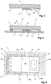
- Figs. 1 and 2 show a sensor assembly according to a first example. It comprises a substrate 1 and a sensor chip 2 as described above. Sensor chip 2 is flip-chip mounted to substrate 1, with a first side 3 of sensor chip 2 facing substrate 1.
- sensing area 4 and the contact pads 5 are both integrated on first side 3 of sensor chip 2, together with any further components integrated on sensor chip 2.
- Sensing area 4 is arranged in a first section of substrate 1, in the following called the “sensing section 7", while the contact pads 5 are arranged in a second section of substrate 1, in the following called the “contact section 8".
- the contact pads 5 are electrically connected to conducting leads 7 on substrate 1 by means of solder bumps 10 as it is known to the skilled person.
- Sensor chip 2 is substantially rectangular having a first lateral edge 9a at the end side of sensing section 7, a second lateral edge 9b extending perpendicular to first lateral edge 9a, a third lateral edge 9c at an end side of contact section 8 and extending perpendicular to second lateral edge 9b, and a fourth lateral edge 9d extending perpendicular to third lateral edge 9c.
- the sensor assembly comprises a dam 16 arranged as a layer extending between sensor chip 2 and substrate 1.
- dam 16 is substantially U-shaped having a base 16a, which extends between second lateral edge 9b and fourth lateral edge 9d, and legs 16b, 16c, which extend from base 16a along fourth lateral edge 9d and second lateral edge 9b, respectively.
- Dam 16 encloses a chamber 17 formed between sensor chip 2 (forming a top side of chamber 17), substrate 1 (forming a bottom side of chamber 17) and dam 16 (forming three of four lateral sides of chamber 17).
- an opening 19 is provided in chamber 17. Opening 19 is arranged between substrate 1, sensor chip 2 and the legs 16b, 16c and extends from a first edge 9a of sensor chip 2 through dam 16 to chamber 17.
- Sensing area 4 is located at least partially in chamber 17 and communicates with the environment through opening 19.
- the underfill 18 is arranged between sensor chip 2 and substrate 1, namely in contact section 8 of sensor chip 2, and is laterally bordered by dam 16.
- Dam 16 prevents underfill 18 from entering chamber 17.
- the legs 16b, 16c of dam 16 advantageously extend all the way to first edge 19a of sensor chip 2, i.e. to the edge where opening 19 is located.
- Figs. 3 and 4 show the steps for manufacturing the sensor assembly.
- Dam 16 has a height substantially equal to the solder bumps 10 that are formed during the later flip-chip mounting step. It is advantageously formed at least partially of a photoresist, in particular SU-8, thus that it can be structured easily.
- photoresist is to be understood as any material that is structured by irradiation and subsequent selective removal of irradiated or non-irradiated parts.
- dam 16 comprises a first layer 20, which is advantageously formed by the photoresist mentioned above, and a second layer 21, which is advantageously an adhesive for being bonded to substrate 1.
- First layer 20 extends from sensor chip 2 to second layer 21, and second layer 21 extends, in the final assembly, from first layer 20 to substrate 1.
- second layer 21 is advantageously an adhesive.
- first layer 21 or substrate 1 prior to flip-chip mounting It may be a glue that bonds upon contact, or it may be a hot-melt adhesive that creates a bond at the elevated temperatures (typically around 260°C) during flip-chip mounting.
- layer 21 can be a UV-curable adhesive, which can be cured by UV-irradiation through substrate 1, or a snap-curable adhesive, which can be cured by heating above a threshold temperature.
- dam 16 is advantageously substantially equal to the height of the solder bumps 10 formed during flip-chip mounting such that sensor chip 2 is aligned substantially parallel to substrate 1.
- dam 16 may be of a material that is softened or even liquefied at the temperatures used during flip-chip mounting, which allows to improve this alignment by adjusting the positioning angle of sensor chip 2.
- underfill 18 is applied, in liquid form, along the edge of sensor chip 2 in the region of contact section 8, drawn into the gap between sensor chip 2 and substrate 1, and hardened. As described above, the blocking action of dam 16 prevents underfill 18 from covering sensing area 4.
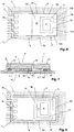
- Fig. 5 shows a second example of a sensor assembly.
- the design of the embodiment of Fig. 5 is the same as the one of Fig. 2 and merely differs in the shape of dam 16.
- dam 16 of the embodiment of Fig. 2 is U-shaped
- dam 16 of Fig. 5 is substantially L-shaped having a base 16a, which extends between second lateral edge 9b and fourth lateral edge 9d, and a leg 16b, which extends from base 16a along fourth lateral edge 9d to first lateral edge 9a.
- chamber 17 is open towards first lateral edge 9a and second lateral edge 9b.
- opening 19 of chamber 17 extends from first lateral edge 9a and second lateral edge 9b through dam 16.
- This example provides better communication of chamber 17 with the environment because opening 19 has a larger diameter. Since underfill is typically applied along two edges of a chip, this sensor design is still compatible with conventional underfilling techniques as long as the underfill is applied from third and fourth edge 9c, 9d only.
- leg 16b of dam 16 can be dispensed with, in which case chamber 17 is open on three sides. In that case, care must be taken to insert underfill 18 only at the side of dam 16 that faces away from chamber 17.
- Fig. 6 shows a third example. It again differs from the embodiment of Fig. 2 in the shape of dam 16 in that the legs 16b and 16c have bent sections 16d and 16e at their ends. The bent sections 16d, 16e extend inwards along first edge 9a, thereby narrowing the diameter of opening 19. This design lessens the risk of underfill 18 or any other foreign bodies entering chamber 17.
- Fig. 7 and 8 differs from the one of Fig. 2 in three aspects.
- a first difference lies in the fact that dam 16 is formed by solder, advantageously by a bump 30 extending all the way around chamber 17 and therefore sensing area 4. It seals chamber 17 against underfill 18. It must be noted, though, that this fourth embodiment does not necessarily require a dam made of solder, but may also use a dam as described in reference to Fig. 3 , and vice versa.
- a second difference lies in the fact that opening 19 is not arranged between substrate 1 and sensor chip 2 but rather extends through sensor chip 2 to the second side 25 of sensor chip 2, with second side 25 being opposite first side 3.
- a third possible difference lies in the fact that dam 16 does not extend to the edges of sensor chip 2, but rather ends at a distance therefrom, such that a gap is formed for receiving underfill 18 all around sensor chip 2, thereby improving the attachment of sensor chip 2 to substrate 1.
- opening 19 can be manufactured e.g. using anisotropic etching or laser drilling.
- Techniques for laser drilling semiconductor wafers are known to the skilled person and are e.g. described in EP 1 677 346 , the disclosure of which is incorporated herein by reference.
- the embodiment differs from the Example of Fig. 1 in that the underside of dam 16, i.e. the side facing substrate 1, comprises one or more recessed sections or gaps 36 that extend parallel to the dam 16. In that case, even if a small gap remains between the underside of dam 16 and substrate 1, underfill 18 may enter a first recess or gap 36, but will generally stop there. Hence, such recessed sections or gaps 36 allow to improve the sealing properties of dam 16 and can even obviate the need to fixedly connect dam 16 to substrate 1.
- underfill 18 has been arranged between sensor chip 2 and substrate 1, at least in the region of contact section 8.
- the dam can also be used to prevent solder flux, which is applied with the solder, from entering sensing area 4.
- the invention is also useful for sensor assemblies that do not use underfill.
- the present invention simplifies the manufacturing process of a sensor assembly because it allows to use conventional flip-chip mounting and does not rely on any opening in substrate 1 to be arranged at the location of chamber 17. In fact, and as shown in the figures, substrate 1 can be closed at the location of chamber 17.
- dam 16 is arranged between sensing section 7 and contact section 8 of sensor chip 2, with sensing area 4 being arranged on a first side thereof and contact pads 5 being arranged at an opposite, second side thereof, such that the contact section 8 can be filled with underfill 18.
Landscapes
- General Physics & Mathematics (AREA)
- Physics & Mathematics (AREA)
- Chemical & Material Sciences (AREA)
- Immunology (AREA)
- Health & Medical Sciences (AREA)
- Life Sciences & Earth Sciences (AREA)
- Chemical Kinetics & Catalysis (AREA)
- General Health & Medical Sciences (AREA)
- Analytical Chemistry (AREA)
- Electrochemistry (AREA)
- Biochemistry (AREA)
- Pathology (AREA)
- Structures Or Materials For Encapsulating Or Coating Semiconductor Devices Or Solid State Devices (AREA)
- Measuring Fluid Pressure (AREA)
- Wire Bonding (AREA)
Description
- The invention relates to a sensor assembly comprising a substrate and a sensor chip flip-chip mounted to the substrate as well as to a method for manufacturing such a sensor.
- Flip-chip mounting of sensor chips to substrates allows for a simple and efficient manufacturing of sensor assemblies, such as e.g. described in
WO 98/27411 DE102005037948 andDE19810060 , where a sensor chip having a sensing area integrated on a first side thereof is mounted to a substrate. The sensing area is structured to measure at least one parameter of the environment, such as environmental humidity or pressure, and has therefore to be accessible. For this reason, a window of the substrate is arranged opposite to the sensing area. Contact pads integrated on the first side of the sensor chip can be used to establish electrical contacts between the sensor chip and the substrate during flip-chip mounting. - Typically, and also as shown in
WO 98/27411 DE102005037948 andDE19810060 , the gap between the sensor chip and the substrate is filled by a filler material, the so-called "underfill". The underfill is typically applied as a liquid to one or two edges of the sensor chip after flip-chip mounting, and the liquid is then drawn into the gap using capillary forces and it is subsequently hardened. - In order to prevent the underfill from covering the sensing area, the sensor assembly of,
DE102005037948 andDE19810060 is provided with a dam extending around the sensing area and the window. Similar dams can be useful for preventing solder flux from covering the sensing area. When flip-chip mounting the sensor chip to the substrate, care must be taken to properly align the window in the substrate, the dam and the sensing area. - The problem to be solved by the present invention is to provide an assembly of the type mentioned above that can be manufactured easily.
- This problem is solved by the sensor assembly of
claim 1. - The invention also relates to a method for manufacturing this type of sensor. The invention can advantageously be used for applications where costs are to be kept low, such as in consumer electronics devices and computer equipment, such as hard disk drives.
- The invention will be better understood and objects other than those set forth above will become apparent when consideration is given to the following detailed description thereof. Such description makes reference to the annexed drawings, wherein:
-
Fig. 1 shows a sectional view of a first sensor assembly, -
Fig. 2 shows a top view of the sensor assembly ofFig. 1 , -
Fig. 3 shows a first manufacturing step of a sensor assembly, -
Fig. 4 shows a second manufacturing step of a sensor assembly -
Fig. 5 shows a top view of a second sensor assembly, -
Fig. 6 shows a top view of a third sensor assembly, -
Fig. 7 shows a sectional view of a fourth sensor assembly, -
Fig. 8 shows a top view of the sensor assembly ofFig. 7 , and -
Fig. 9 shows a sectional view of a fifth sensor assembly according to the invention. - The sensor assembly described below comprises a sensor chip with a sensing area integrated thereon. The sensor chip is advantageously a semiconductor chip, but it may e.g. also be a glass or ceramics chip. Semiconductor chips have the advantage that they allow for direct integration of further circuitry thereon.
- The sensing area can e.g. comprise a humidity sensor and/or a pressure sensor. It is e.g. formed by a flexible membrane of a pressure sensor or a moisture adsorbing material and a set of electrodes in the case of a humidity sensor.
- A pressure sensor can e.g. be structured as disclosed in
EP 1 860 418 - A humidity sensor can e.g. be structured as disclosed in
US 6 690 569 . - As e.g. described in
US 6 690 569 , in addition to a sensing area and contact pads, the sensor chip may also have further elements integrated thereon, in particular passive and active circuitry, such as amplifiers, filters, A/D- or D/A-converters, digital processing circuitry, etc. - The assembly described below further comprises a substrate. The substrate is typically a printed circuit board having conducting leads mounted thereon. Advantageously, the substrate is a flexible printed circuit board. The term "flexible printed circuit board" refers to an electrically insulating substrate that has circuit leads integrated thereon and that can be reversibly bent to a radius of 1 cm or smaller.
-
Figs. 1 and 2 show a sensor assembly according to a first example. It comprises asubstrate 1 and asensor chip 2 as described above.Sensor chip 2 is flip-chip mounted tosubstrate 1, with afirst side 3 ofsensor chip 2 facingsubstrate 1. - The
sensing area 4 and thecontact pads 5 are both integrated onfirst side 3 ofsensor chip 2, together with any further components integrated onsensor chip 2.Sensing area 4 is arranged in a first section ofsubstrate 1, in the following called the "sensing section 7", while thecontact pads 5 are arranged in a second section ofsubstrate 1, in the following called the "contact section 8". - The
contact pads 5 are electrically connected to conductingleads 7 onsubstrate 1 by means ofsolder bumps 10 as it is known to the skilled person. -
Sensor chip 2 is substantially rectangular having a firstlateral edge 9a at the end side ofsensing section 7, a secondlateral edge 9b extending perpendicular to firstlateral edge 9a, a thirdlateral edge 9c at an end side ofcontact section 8 and extending perpendicular to secondlateral edge 9b, and a fourthlateral edge 9d extending perpendicular to thirdlateral edge 9c. - The sensor assembly comprises a
dam 16 arranged as a layer extending betweensensor chip 2 andsubstrate 1. In the embodiment ofFigs. 1 and 2 ,dam 16 is substantially U-shaped having abase 16a, which extends between secondlateral edge 9b and fourthlateral edge 9d, andlegs base 16a along fourthlateral edge 9d and secondlateral edge 9b, respectively.Dam 16 encloses achamber 17 formed between sensor chip 2 (forming a top side of chamber 17), substrate 1 (forming a bottom side of chamber 17) and dam 16 (forming three of four lateral sides of chamber 17). At one lateral side (left hand side inFigs. 1 and 2 ) anopening 19 is provided inchamber 17.Opening 19 is arranged betweensubstrate 1,sensor chip 2 and thelegs first edge 9a ofsensor chip 2 throughdam 16 tochamber 17. -
Sensing area 4 is located at least partially inchamber 17 and communicates with the environment through opening 19. - The
underfill 18 is arranged betweensensor chip 2 andsubstrate 1, namely incontact section 8 ofsensor chip 2, and is laterally bordered bydam 16.Dam 16 preventsunderfill 18 from enteringchamber 17. In order to minimize the risk ofunderfill 18 enteringchamber 17, thelegs dam 16 advantageously extend all the way to first edge 19a ofsensor chip 2, i.e. to the edge whereopening 19 is located. -
Figs. 3 and 4 show the steps for manufacturing the sensor assembly. - First,
sensor chip 2 is provided, withsensing area 4 andcontact pads 5 integrated on itsfirst side 3. Next,dam 16 is applied tofirst side 3.Dam 16 has a height substantially equal to thesolder bumps 10 that are formed during the later flip-chip mounting step. It is advantageously formed at least partially of a photoresist, in particular SU-8, thus that it can be structured easily. - The term "photoresist" is to be understood as any material that is structured by irradiation and subsequent selective removal of irradiated or non-irradiated parts.
- In the example shown in
Figs. 1 - 4 ,dam 16 comprises afirst layer 20, which is advantageously formed by the photoresist mentioned above, and asecond layer 21, which is advantageously an adhesive for being bonded tosubstrate 1.First layer 20 extends fromsensor chip 2 tosecond layer 21, andsecond layer 21 extends, in the final assembly, fromfirst layer 20 tosubstrate 1. - In a next step, the parts shown in
Fig. 3 are flip-chip mounted tosubstrate 1 and the solder bumps 10 are formed to create the electrical connections between thecontact pads 5 and theleads 7. At the same time,dam 16 is bonded tosubstrate 1, in the embodiment shown here by means ofsecond layer 21. As mentioned,second layer 21 is advantageously an adhesive. For example, it can be applied to eitherfirst layer 21 orsubstrate 1 prior to flip-chip mounting. It may be a glue that bonds upon contact, or it may be a hot-melt adhesive that creates a bond at the elevated temperatures (typically around 260°C) during flip-chip mounting. Also,layer 21 can be a UV-curable adhesive, which can be cured by UV-irradiation throughsubstrate 1, or a snap-curable adhesive, which can be cured by heating above a threshold temperature. - As mentioned above, the height of
dam 16 is advantageously substantially equal to the height of the solder bumps 10 formed during flip-chip mounting such thatsensor chip 2 is aligned substantially parallel tosubstrate 1. Optionally,dam 16 may be of a material that is softened or even liquefied at the temperatures used during flip-chip mounting, which allows to improve this alignment by adjusting the positioning angle ofsensor chip 2. - After flip-chip mounting, underfill 18 is applied, in liquid form, along the edge of
sensor chip 2 in the region ofcontact section 8, drawn into the gap betweensensor chip 2 andsubstrate 1, and hardened. As described above, the blocking action ofdam 16 prevents underfill 18 from coveringsensing area 4. -
Fig. 5 shows a second example of a sensor assembly. The design of the embodiment ofFig. 5 is the same as the one ofFig. 2 and merely differs in the shape ofdam 16. Whiledam 16 of the embodiment ofFig. 2 is U-shaped,dam 16 ofFig. 5 is substantially L-shaped having abase 16a, which extends between secondlateral edge 9b and fourthlateral edge 9d, and aleg 16b, which extends frombase 16a along fourthlateral edge 9d to firstlateral edge 9a. Hence, in this embodiment,chamber 17 is open towards firstlateral edge 9a and secondlateral edge 9b. In other words, opening 19 ofchamber 17 extends from firstlateral edge 9a and secondlateral edge 9b throughdam 16. - This example provides better communication of
chamber 17 with the environment because opening 19 has a larger diameter. Since underfill is typically applied along two edges of a chip, this sensor design is still compatible with conventional underfilling techniques as long as the underfill is applied from third andfourth edge - In a further example (not shown)
leg 16b ofdam 16 can be dispensed with, in whichcase chamber 17 is open on three sides. In that case, care must be taken to insertunderfill 18 only at the side ofdam 16 that faces away fromchamber 17. -
Fig. 6 shows a third example. It again differs from the embodiment ofFig. 2 in the shape ofdam 16 in that thelegs sections bent sections first edge 9a, thereby narrowing the diameter ofopening 19. This design lessens the risk ofunderfill 18 or any other foreignbodies entering chamber 17. - The example of
Fig. 7 and 8 differs from the one ofFig. 2 in three aspects. - A first difference lies in the fact that
dam 16 is formed by solder, advantageously by abump 30 extending all the way aroundchamber 17 and therefore sensingarea 4. It sealschamber 17 againstunderfill 18. It must be noted, though, that this fourth embodiment does not necessarily require a dam made of solder, but may also use a dam as described in reference toFig. 3 , and vice versa. - A second difference lies in the fact that opening 19 is not arranged between
substrate 1 andsensor chip 2 but rather extends throughsensor chip 2 to thesecond side 25 ofsensor chip 2, withsecond side 25 being oppositefirst side 3. - A third possible difference lies in the fact that
dam 16 does not extend to the edges ofsensor chip 2, but rather ends at a distance therefrom, such that a gap is formed for receivingunderfill 18 all aroundsensor chip 2, thereby improving the attachment ofsensor chip 2 tosubstrate 1. - In the embodiment of
Figs. 7 and 8 , opening 19 can be manufactured e.g. using anisotropic etching or laser drilling. Techniques for laser drilling semiconductor wafers are known to the skilled person and are e.g. described inEP 1 677 346 - The embodiment differs from the Example of
Fig. 1 in that the underside ofdam 16, i.e. theside facing substrate 1, comprises one or more recessed sections orgaps 36 that extend parallel to thedam 16. In that case, even if a small gap remains between the underside ofdam 16 andsubstrate 1, underfill 18 may enter a first recess orgap 36, but will generally stop there. Hence, such recessed sections orgaps 36 allow to improve the sealing properties ofdam 16 and can even obviate the need to fixedly connectdam 16 tosubstrate 1. - In the embodiment described above, underfill 18 has been arranged between
sensor chip 2 andsubstrate 1, at least in the region ofcontact section 8. As mentioned, though, the dam can also be used to prevent solder flux, which is applied with the solder, from enteringsensing area 4. Hence, the invention is also useful for sensor assemblies that do not use underfill. - The present invention simplifies the manufacturing process of a sensor assembly because it allows to use conventional flip-chip mounting and does not rely on any opening in
substrate 1 to be arranged at the location ofchamber 17. In fact, and as shown in the figures,substrate 1 can be closed at the location ofchamber 17. - Typically,
dam 16 is arranged betweensensing section 7 andcontact section 8 ofsensor chip 2, withsensing area 4 being arranged on a first side thereof andcontact pads 5 being arranged at an opposite, second side thereof, such that thecontact section 8 can be filled withunderfill 18. - While there are shown and described presently preferred embodiments of the invention, it is to be distinctly understood that the invention is not limited thereto but may be otherwise variously embodied and practiced within the scope of the following claims.
Claims (13)
- A sensor assembly comprising
a substrate (1),
a sensor chip (2) flip-chip mounted to said substrate (1) with a first side (3) of said sensor chip (3) facing said substrate (1),
a sensing area (4) integrated on the first side (3) of said sensor chip (2), wherein said sensing area (4) is structured to measure at least one parameter,
contact pads (5) integrated on the first side (3) of said sensor chip (2) in a contact section (8) of said sensor chip (2), wherein said contact pads (5) are electrically connected to said substrate (1),
a dam (16) extending between said sensor chip (2) and said substrate (1), wherein a chamber (17) is formed between said sensor chip (2), said substrate (1) and said dam (16), with said sensing area (4) being located at least partially in said chamber (17) and with said dam (16) being arranged between said contact section (8) and said chamber (17), and
an underfill (18) or solder flux arranged in said contact section (8) between said sensor chip (2) and said substrate (1), wherein said dam (16) is arranged between said underfill (18) and said sensing area (4), and
at least one opening extending from said chamber (17) to an environment around said sensor assembly, wherein said opening is arranged between said substrate (1) and said sensor chip (2) and/or extends through said sensor chip (2),
characterized in that said dam (16) comprises one or more recesses or gaps (36) extending parallel to said dam (16). - The sensor assembly of claim 1 wherein said opening (17) is arranged between said substrate (1) and said sensor chip (2) and extends from at least a first edge (9a) of said sensor chip (2) to said chamber (17).
- The sensor assembly of claim 2 wherein said dam (16) extends to said first edge (9a).
- The sensor assembly of claim 3 wherein said opening (17) extends from a first edge (9a) and a second edge (9b) of said sensor chip (2) to said chamber (17) and wherein said dam (16) extends to said first edge (9a) and said second edge (9b), wherein said first edge (9a) is adjacent to said second edge (9b).
- The sensor of claim 3 wherein said dam comprises a base (16a) extending from a second edge (9b) to a fourth edge (9d) of said sensor chip (2), a first leg (16b) extending from said base (16a) along said fourth edge (9d) of said sensor chip (2) to said first edge (9a) of said sensor chip (2), and a second leg (16c) extending from said base (16a) along said second edge (9d) of said sensor chip (2) to said first edge (9a) of said sensor chip (2), and wherein said opening (17) is formed between said first and second legs (16b, 16c).
- The sensor assembly of claim 1 wherein said opening extends through said sensor substrate (2) and wherein said dam (16) extends sealingly around said chamber (17).
- The sensor assembly of any of the preceding claims wherein said dam (16) comprises a photoresist, in particular SU-8.
- The sensor assembly of any of the preceding claims wherein said dam (16) comprises a first layer (20) and a second layer (21), wherein said first layer (20) extends from said sensor chip (2) and wherein said second layer (21) extends to said substrate (1), wherein said second layer (21) is an adhesive.
- The sensor assembly of any of the preceding claims wherein said substrate (1) is a flexible printed circuit board.
- The sensor assembly of any of the preceding claims wherein said sensing area (4) comprises a humidity sensor and/or a pressure sensor.
- The sensor assembly of any of the preceding claims wherein said sensing area (4) is arranged at a first side of said dam (16) and said contact pads (5) are arranged at a second, opposite side of said dam (16).
- A method for manufacturing the sensor assembly of any of the preceding claims comprising the steps of
flip-chip mounting said sensor chip (2) to said substrate (1), and
applying underfill (18) or solder flux between said contact section (8) and said substrate (1), with said dam (16) comprising one or more recesses or gaps (36) extending parallel to said dam (16) being arranged between said underfill (18) or solder flux and said sensing area (4). - The method of claim 12, wherein said dam (16) is adhesively bonded to said substrate (1) using a glue, a hot-melt adhesive, a UV-curable adhesive or a snap-curable adhesive.
Applications Claiming Priority (1)
| Application Number | Priority Date | Filing Date | Title |
|---|---|---|---|
| PCT/CH2009/000367 WO2011060558A1 (en) | 2009-11-18 | 2009-11-18 | Sensor mounted in flip-chip technology on a substrate |
Publications (2)
| Publication Number | Publication Date |
|---|---|
| EP2502066A1 EP2502066A1 (en) | 2012-09-26 |
| EP2502066B1 true EP2502066B1 (en) | 2017-09-27 |
Family
ID=42314747
Family Applications (1)
| Application Number | Title | Priority Date | Filing Date |
|---|---|---|---|
| EP09756134.4A Active EP2502066B1 (en) | 2009-11-18 | 2009-11-18 | Sensor mounted in flip-chip technology on a substrate and its manufacture |
Country Status (3)
| Country | Link |
|---|---|
| US (1) | US8791532B2 (en) |
| EP (1) | EP2502066B1 (en) |
| WO (1) | WO2011060558A1 (en) |
Families Citing this family (57)
| Publication number | Priority date | Publication date | Assignee | Title |
|---|---|---|---|---|
| US8791532B2 (en) | 2009-11-18 | 2014-07-29 | Sensirion Ag | Sensor mounted in flip-chip technology on a substrate |
| US8736002B2 (en) | 2009-11-18 | 2014-05-27 | Sensirion Ag | Sensor mounted in flip-chip technology at a substrate edge |
| US9917647B2 (en) * | 2012-01-31 | 2018-03-13 | Hewlett Packard Enterprise Development Lp | Combination underfill-dam and electrical-interconnect structure for an opto-electronic engine |
| US9812350B2 (en) | 2013-03-06 | 2017-11-07 | Qorvo Us, Inc. | Method of manufacture for a silicon-on-plastic semiconductor device with interfacial adhesion layer |
| US9583414B2 (en) | 2013-10-31 | 2017-02-28 | Qorvo Us, Inc. | Silicon-on-plastic semiconductor device and method of making the same |
| US9503622B2 (en) | 2014-03-10 | 2016-11-22 | Apple Inc. | Preventing artifacts due to underfill in flip chip imager assembly |
| TWI582847B (en) | 2014-09-12 | 2017-05-11 | Rf微型儀器公司 | Printed circuit module including semiconductor device having polymer substrate and method of manufacturing the same |
| EP3001186B1 (en) | 2014-09-26 | 2018-06-06 | Sensirion AG | Sensor chip |
| US10085352B2 (en) | 2014-10-01 | 2018-09-25 | Qorvo Us, Inc. | Method for manufacturing an integrated circuit package |
| US10121718B2 (en) | 2014-11-03 | 2018-11-06 | Qorvo Us, Inc. | Printed circuit module having a semiconductor device with a protective layer in place of a low-resistivity handle layer |
| JP6425595B2 (en) | 2015-03-24 | 2018-11-21 | アルプス電気株式会社 | Electronic component and method of manufacturing electronic component |
| US9960145B2 (en) | 2015-03-25 | 2018-05-01 | Qorvo Us, Inc. | Flip chip module with enhanced properties |
| US9613831B2 (en) | 2015-03-25 | 2017-04-04 | Qorvo Us, Inc. | Encapsulated dies with enhanced thermal performance |
| US20160343604A1 (en) | 2015-05-22 | 2016-11-24 | Rf Micro Devices, Inc. | Substrate structure with embedded layer for post-processing silicon handle elimination |
| US10276495B2 (en) | 2015-09-11 | 2019-04-30 | Qorvo Us, Inc. | Backside semiconductor die trimming |
| DE102015218355A1 (en) * | 2015-09-24 | 2017-03-30 | Robert Bosch Gmbh | Microelectronic component arrangement and production method for a microelectronic component arrangement |
| US10020405B2 (en) * | 2016-01-19 | 2018-07-10 | Qorvo Us, Inc. | Microelectronics package with integrated sensors |
| US10090262B2 (en) | 2016-05-09 | 2018-10-02 | Qorvo Us, Inc. | Microelectronics package with inductive element and magnetically enhanced mold compound component |
| US10784149B2 (en) | 2016-05-20 | 2020-09-22 | Qorvo Us, Inc. | Air-cavity module with enhanced device isolation |
| US10773952B2 (en) | 2016-05-20 | 2020-09-15 | Qorvo Us, Inc. | Wafer-level package with enhanced performance |
| US10103080B2 (en) | 2016-06-10 | 2018-10-16 | Qorvo Us, Inc. | Thermally enhanced semiconductor package with thermal additive and process for making the same |
| US10079196B2 (en) | 2016-07-18 | 2018-09-18 | Qorvo Us, Inc. | Thermally enhanced semiconductor package having field effect transistors with back-gate feature |
| CN109844937B (en) | 2016-08-12 | 2023-06-27 | Qorvo美国公司 | Wafer-level packaging with enhanced performance |
| US10109550B2 (en) | 2016-08-12 | 2018-10-23 | Qorvo Us, Inc. | Wafer-level package with enhanced performance |
| JP7022112B2 (en) | 2016-08-12 | 2022-02-17 | コーボ ユーエス,インコーポレイティド | Wafer level package with improved performance |
| EP3139159A1 (en) | 2016-08-23 | 2017-03-08 | Sensirion AG | Sensor assembly |
| US10109502B2 (en) | 2016-09-12 | 2018-10-23 | Qorvo Us, Inc. | Semiconductor package with reduced parasitic coupling effects and process for making the same |
| US10090339B2 (en) | 2016-10-21 | 2018-10-02 | Qorvo Us, Inc. | Radio frequency (RF) switch |
| US10749518B2 (en) | 2016-11-18 | 2020-08-18 | Qorvo Us, Inc. | Stacked field-effect transistor switch |
| US10068831B2 (en) | 2016-12-09 | 2018-09-04 | Qorvo Us, Inc. | Thermally enhanced semiconductor package and process for making the same |
| US10755992B2 (en) | 2017-07-06 | 2020-08-25 | Qorvo Us, Inc. | Wafer-level packaging for enhanced performance |
| US10366972B2 (en) | 2017-09-05 | 2019-07-30 | Qorvo Us, Inc. | Microelectronics package with self-aligned stacked-die assembly |
| US10784233B2 (en) | 2017-09-05 | 2020-09-22 | Qorvo Us, Inc. | Microelectronics package with self-aligned stacked-die assembly |
| JP7028262B2 (en) * | 2018-01-23 | 2022-03-02 | 株式会社村田製作所 | Substrate bonding structure and substrate bonding method |
| US11152363B2 (en) | 2018-03-28 | 2021-10-19 | Qorvo Us, Inc. | Bulk CMOS devices with enhanced performance and methods of forming the same utilizing bulk CMOS process |
| WO2019195428A1 (en) | 2018-04-04 | 2019-10-10 | Qorvo Us, Inc. | Gallium-nitride-based module with enhanced electrical performance and process for making the same |
| US12046505B2 (en) | 2018-04-20 | 2024-07-23 | Qorvo Us, Inc. | RF devices with enhanced performance and methods of forming the same utilizing localized SOI formation |
| US10804246B2 (en) | 2018-06-11 | 2020-10-13 | Qorvo Us, Inc. | Microelectronics package with vertically stacked dies |
| CN112534553B (en) | 2018-07-02 | 2024-03-29 | Qorvo美国公司 | RF semiconductor device and method for manufacturing the same |
| US10964554B2 (en) | 2018-10-10 | 2021-03-30 | Qorvo Us, Inc. | Wafer-level fan-out package with enhanced performance |
| US11069590B2 (en) | 2018-10-10 | 2021-07-20 | Qorvo Us, Inc. | Wafer-level fan-out package with enhanced performance |
| US11646242B2 (en) | 2018-11-29 | 2023-05-09 | Qorvo Us, Inc. | Thermally enhanced semiconductor package with at least one heat extractor and process for making the same |
| CN113632209B (en) | 2019-01-23 | 2026-05-12 | Qorvo美国公司 | RF semiconductor device and method for manufacturing the same |
| US12057374B2 (en) | 2019-01-23 | 2024-08-06 | Qorvo Us, Inc. | RF devices with enhanced performance and methods of forming the same |
| US11387157B2 (en) | 2019-01-23 | 2022-07-12 | Qorvo Us, Inc. | RF devices with enhanced performance and methods of forming the same |
| US12046483B2 (en) | 2019-01-23 | 2024-07-23 | Qorvo Us, Inc. | RF devices with enhanced performance and methods of forming the same |
| US12125825B2 (en) | 2019-01-23 | 2024-10-22 | Qorvo Us, Inc. | RF devices with enhanced performance and methods of forming the same |
| US12046570B2 (en) | 2019-01-23 | 2024-07-23 | Qorvo Us, Inc. | RF devices with enhanced performance and methods of forming the same |
| KR102565715B1 (en) | 2019-05-03 | 2023-08-10 | 삼성전자주식회사 | Semiconductor package |
| US12074086B2 (en) | 2019-11-01 | 2024-08-27 | Qorvo Us, Inc. | RF devices with nanotube particles for enhanced performance and methods of forming the same |
| US11646289B2 (en) | 2019-12-02 | 2023-05-09 | Qorvo Us, Inc. | RF devices with enhanced performance and methods of forming the same |
| US11923238B2 (en) | 2019-12-12 | 2024-03-05 | Qorvo Us, Inc. | Method of forming RF devices with enhanced performance including attaching a wafer to a support carrier by a bonding technique without any polymer adhesive |
| US12129168B2 (en) | 2019-12-23 | 2024-10-29 | Qorvo Us, Inc. | Microelectronics package with vertically stacked MEMS device and controller device |
| US11664340B2 (en) * | 2020-07-13 | 2023-05-30 | Analog Devices, Inc. | Negative fillet for mounting an integrated device die to a carrier |
| US12482731B2 (en) | 2020-12-11 | 2025-11-25 | Qorvo Us, Inc. | Multi-level 3D stacked package and methods of forming the same |
| WO2022186857A1 (en) | 2021-03-05 | 2022-09-09 | Qorvo Us, Inc. | Selective etching process for si-ge and doped epitaxial silicon |
| US20240021566A1 (en) * | 2022-07-15 | 2024-01-18 | STATS ChipPAC Pte. Ltd. | Semiconductor Device and Method of Forming Underfill Dam for Chip-to-Wafer Device |
Family Cites Families (16)
| Publication number | Priority date | Publication date | Assignee | Title |
|---|---|---|---|---|
| US5840500A (en) | 1996-07-11 | 1998-11-24 | Trega Biosciences, Inc. | Quinoline derivatives and quinoline combinatorial libraries |
| US6140144A (en) | 1996-08-08 | 2000-10-31 | Integrated Sensing Systems, Inc. | Method for packaging microsensors |
| ATE214476T1 (en) * | 1996-12-17 | 2002-03-15 | Lab Fuer Physikalische Elektro | METHOD FOR APPLYING A MICROSYSTEM OR TRANSDUCER TO A SUBSTRATE AND DEVICE PRODUCABLE BY THIS METHOD |
| DE19810060B4 (en) | 1997-05-07 | 2005-10-13 | Fraunhofer-Gesellschaft zur Förderung der angewandten Forschung e.V. | A method of connecting a device to a substrate and an electrical circuit made therewith |
| DE19852967B4 (en) * | 1998-11-17 | 2004-05-27 | Micronas Gmbh | Measuring device with a semiconductor arrangement |
| AU6719000A (en) | 1999-12-08 | 2001-06-18 | Sensirion Ag | Capacitive sensor |
| EP1380481B1 (en) | 2000-02-11 | 2004-08-18 | E + E Elektronik Gesellschaft M.B.H. | Sensor arrangement |
| WO2003028949A2 (en) | 2001-10-01 | 2003-04-10 | Xsil Technology Limited | Method of machining substrates |
| US20060177349A1 (en) | 2003-03-18 | 2006-08-10 | Jacob Thaysen | Chemical sensor |
| US20050104186A1 (en) | 2003-11-14 | 2005-05-19 | International Semiconductor Technology Ltd. | Chip-on-film package for image sensor and method for manufacturing the same |
| US7038321B1 (en) * | 2005-04-29 | 2006-05-02 | Delphi Technologies, Inc. | Method of attaching a flip chip device and circuit assembly formed thereby |
| DE102005037948A1 (en) * | 2005-08-11 | 2007-02-15 | Robert Bosch Gmbh | Sensor arrangement with a sensor component and a carrier and method for producing a sensor arrangement |
| EP1860418A1 (en) | 2006-05-23 | 2007-11-28 | Sensirion AG | A method for fabricating a pressure sensor using SOI wafers |
| JP2008261670A (en) | 2007-04-10 | 2008-10-30 | Toshiba Corp | Detector and manufacturing method thereof |
| US8736002B2 (en) | 2009-11-18 | 2014-05-27 | Sensirion Ag | Sensor mounted in flip-chip technology at a substrate edge |
| US8791532B2 (en) | 2009-11-18 | 2014-07-29 | Sensirion Ag | Sensor mounted in flip-chip technology on a substrate |
-
2009
- 2009-11-18 US US13/498,371 patent/US8791532B2/en active Active
- 2009-11-18 WO PCT/CH2009/000367 patent/WO2011060558A1/en not_active Ceased
- 2009-11-18 EP EP09756134.4A patent/EP2502066B1/en active Active
Non-Patent Citations (1)
| Title |
|---|
| None * |
Also Published As
| Publication number | Publication date |
|---|---|
| US8791532B2 (en) | 2014-07-29 |
| EP2502066A1 (en) | 2012-09-26 |
| WO2011060558A1 (en) | 2011-05-26 |
| US20120267731A1 (en) | 2012-10-25 |
Similar Documents
| Publication | Publication Date | Title |
|---|---|---|
| US8791532B2 (en) | Sensor mounted in flip-chip technology on a substrate | |
| EP2502067B1 (en) | Sensor mounted in flip-chip technology at a substrate edge | |
| US6166434A (en) | Die clip assembly for semiconductor package | |
| JP5104734B2 (en) | Highly reliable semiconductor device production method and system | |
| CN100580918C (en) | Package structure capable of reducing package stress | |
| US20030189262A1 (en) | Method and apparatus for attaching microelectronic substrates and support members | |
| TW200840012A (en) | Semiconductor package, integrated circuit cards incorporating the semiconductor package, and method of manufacturing the same | |
| CN205177808U (en) | Chip packaging structure | |
| US8358018B2 (en) | Resin sealing structure for electronic component and resin sealing method for electronic component | |
| JP2009503837A (en) | Package for microelectronic component and manufacturing method thereof | |
| TW201724612A (en) | Cap structure and semiconductor device package including capping structure | |
| US9142693B2 (en) | Optoelectronic package and method for making same | |
| KR20090130612A (en) | Wafer level package and manufacturing method thereof | |
| WO2009028538A1 (en) | Semiconductor element and method for manufacturing the same | |
| JP2009049115A (en) | Semiconductor device and manufacturing method thereof | |
| CN116582101A (en) | Filter packaging structure and packaging method | |
| JP4688443B2 (en) | Manufacturing method of semiconductor device | |
| JP2797598B2 (en) | Hybrid integrated circuit board | |
| KR100631997B1 (en) | Stack chip package | |
| US8222726B2 (en) | Semiconductor device package having a jumper chip and method of fabricating the same | |
| TW201705412A (en) | Method for manufacturing microelectronic component device and microelectronic component device | |
| KR101019706B1 (en) | Semiconductor package and manufacturing method thereof | |
| JP4436748B2 (en) | Semiconductor device and mounting method thereof | |
| KR100791575B1 (en) | Tape Carrier Semiconductor Device | |
| KR20120126369A (en) | Method for fabricating semiconductoer package |
Legal Events
| Date | Code | Title | Description |
|---|---|---|---|
| PUAI | Public reference made under article 153(3) epc to a published international application that has entered the european phase |
Free format text: ORIGINAL CODE: 0009012 |
|
| 17P | Request for examination filed |
Effective date: 20120327 |
|
| AK | Designated contracting states |
Kind code of ref document: A1 Designated state(s): AT BE BG CH CY CZ DE DK EE ES FI FR GB GR HR HU IE IS IT LI LT LU LV MC MK MT NL NO PL PT RO SE SI SK SM TR |
|
| DAX | Request for extension of the european patent (deleted) | ||
| GRAP | Despatch of communication of intention to grant a patent |
Free format text: ORIGINAL CODE: EPIDOSNIGR1 |
|
| STAA | Information on the status of an ep patent application or granted ep patent |
Free format text: STATUS: GRANT OF PATENT IS INTENDED |
|
| RIC1 | Information provided on ipc code assigned before grant |
Ipc: H01L 21/56 20060101ALI20170509BHEP Ipc: G01N 27/12 20060101ALI20170509BHEP Ipc: G01L 19/14 20060101ALI20170509BHEP Ipc: G01N 33/00 20060101AFI20170509BHEP |
|
| INTG | Intention to grant announced |
Effective date: 20170523 |
|
| GRAS | Grant fee paid |
Free format text: ORIGINAL CODE: EPIDOSNIGR3 |
|
| GRAA | (expected) grant |
Free format text: ORIGINAL CODE: 0009210 |
|
| STAA | Information on the status of an ep patent application or granted ep patent |
Free format text: STATUS: THE PATENT HAS BEEN GRANTED |
|
| AK | Designated contracting states |
Kind code of ref document: B1 Designated state(s): AT BE BG CH CY CZ DE DK EE ES FI FR GB GR HR HU IE IS IT LI LT LU LV MC MK MT NL NO PL PT RO SE SI SK SM TR |
|
| REG | Reference to a national code |
Ref country code: GB Ref legal event code: FG4D |
|
| REG | Reference to a national code |
Ref country code: CH Ref legal event code: EP |
|
| REG | Reference to a national code |
Ref country code: AT Ref legal event code: REF Ref document number: 932416 Country of ref document: AT Kind code of ref document: T Effective date: 20171015 |
|
| REG | Reference to a national code |
Ref country code: IE Ref legal event code: FG4D |
|
| REG | Reference to a national code |
Ref country code: DE Ref legal event code: R096 Ref document number: 602009048573 Country of ref document: DE |
|
| PG25 | Lapsed in a contracting state [announced via postgrant information from national office to epo] |
Ref country code: SE Free format text: LAPSE BECAUSE OF FAILURE TO SUBMIT A TRANSLATION OF THE DESCRIPTION OR TO PAY THE FEE WITHIN THE PRESCRIBED TIME-LIMIT Effective date: 20170927 Ref country code: NO Free format text: LAPSE BECAUSE OF FAILURE TO SUBMIT A TRANSLATION OF THE DESCRIPTION OR TO PAY THE FEE WITHIN THE PRESCRIBED TIME-LIMIT Effective date: 20171227 Ref country code: LT Free format text: LAPSE BECAUSE OF FAILURE TO SUBMIT A TRANSLATION OF THE DESCRIPTION OR TO PAY THE FEE WITHIN THE PRESCRIBED TIME-LIMIT Effective date: 20170927 Ref country code: HR Free format text: LAPSE BECAUSE OF FAILURE TO SUBMIT A TRANSLATION OF THE DESCRIPTION OR TO PAY THE FEE WITHIN THE PRESCRIBED TIME-LIMIT Effective date: 20170927 Ref country code: FI Free format text: LAPSE BECAUSE OF FAILURE TO SUBMIT A TRANSLATION OF THE DESCRIPTION OR TO PAY THE FEE WITHIN THE PRESCRIBED TIME-LIMIT Effective date: 20170927 |
|
| REG | Reference to a national code |
Ref country code: NL Ref legal event code: MP Effective date: 20170927 |
|
| REG | Reference to a national code |
Ref country code: LT Ref legal event code: MG4D |
|
| REG | Reference to a national code |
Ref country code: AT Ref legal event code: MK05 Ref document number: 932416 Country of ref document: AT Kind code of ref document: T Effective date: 20170927 |
|
| PG25 | Lapsed in a contracting state [announced via postgrant information from national office to epo] |
Ref country code: GR Free format text: LAPSE BECAUSE OF FAILURE TO SUBMIT A TRANSLATION OF THE DESCRIPTION OR TO PAY THE FEE WITHIN THE PRESCRIBED TIME-LIMIT Effective date: 20171228 Ref country code: LV Free format text: LAPSE BECAUSE OF FAILURE TO SUBMIT A TRANSLATION OF THE DESCRIPTION OR TO PAY THE FEE WITHIN THE PRESCRIBED TIME-LIMIT Effective date: 20170927 Ref country code: BG Free format text: LAPSE BECAUSE OF FAILURE TO SUBMIT A TRANSLATION OF THE DESCRIPTION OR TO PAY THE FEE WITHIN THE PRESCRIBED TIME-LIMIT Effective date: 20171227 |
|
| PG25 | Lapsed in a contracting state [announced via postgrant information from national office to epo] |
Ref country code: NL Free format text: LAPSE BECAUSE OF FAILURE TO SUBMIT A TRANSLATION OF THE DESCRIPTION OR TO PAY THE FEE WITHIN THE PRESCRIBED TIME-LIMIT Effective date: 20170927 |
|
| PG25 | Lapsed in a contracting state [announced via postgrant information from national office to epo] |
Ref country code: RO Free format text: LAPSE BECAUSE OF FAILURE TO SUBMIT A TRANSLATION OF THE DESCRIPTION OR TO PAY THE FEE WITHIN THE PRESCRIBED TIME-LIMIT Effective date: 20170927 Ref country code: ES Free format text: LAPSE BECAUSE OF FAILURE TO SUBMIT A TRANSLATION OF THE DESCRIPTION OR TO PAY THE FEE WITHIN THE PRESCRIBED TIME-LIMIT Effective date: 20170927 Ref country code: CZ Free format text: LAPSE BECAUSE OF FAILURE TO SUBMIT A TRANSLATION OF THE DESCRIPTION OR TO PAY THE FEE WITHIN THE PRESCRIBED TIME-LIMIT Effective date: 20170927 |
|
| PG25 | Lapsed in a contracting state [announced via postgrant information from national office to epo] |
Ref country code: EE Free format text: LAPSE BECAUSE OF FAILURE TO SUBMIT A TRANSLATION OF THE DESCRIPTION OR TO PAY THE FEE WITHIN THE PRESCRIBED TIME-LIMIT Effective date: 20170927 Ref country code: IT Free format text: LAPSE BECAUSE OF FAILURE TO SUBMIT A TRANSLATION OF THE DESCRIPTION OR TO PAY THE FEE WITHIN THE PRESCRIBED TIME-LIMIT Effective date: 20170927 Ref country code: IS Free format text: LAPSE BECAUSE OF FAILURE TO SUBMIT A TRANSLATION OF THE DESCRIPTION OR TO PAY THE FEE WITHIN THE PRESCRIBED TIME-LIMIT Effective date: 20180127 Ref country code: AT Free format text: LAPSE BECAUSE OF FAILURE TO SUBMIT A TRANSLATION OF THE DESCRIPTION OR TO PAY THE FEE WITHIN THE PRESCRIBED TIME-LIMIT Effective date: 20170927 Ref country code: SM Free format text: LAPSE BECAUSE OF FAILURE TO SUBMIT A TRANSLATION OF THE DESCRIPTION OR TO PAY THE FEE WITHIN THE PRESCRIBED TIME-LIMIT Effective date: 20170927 Ref country code: SK Free format text: LAPSE BECAUSE OF FAILURE TO SUBMIT A TRANSLATION OF THE DESCRIPTION OR TO PAY THE FEE WITHIN THE PRESCRIBED TIME-LIMIT Effective date: 20170927 |
|
| REG | Reference to a national code |
Ref country code: DE Ref legal event code: R097 Ref document number: 602009048573 Country of ref document: DE |
|
| PG25 | Lapsed in a contracting state [announced via postgrant information from national office to epo] |
Ref country code: MC Free format text: LAPSE BECAUSE OF FAILURE TO SUBMIT A TRANSLATION OF THE DESCRIPTION OR TO PAY THE FEE WITHIN THE PRESCRIBED TIME-LIMIT Effective date: 20170927 |
|
| PG25 | Lapsed in a contracting state [announced via postgrant information from national office to epo] |
Ref country code: DK Free format text: LAPSE BECAUSE OF FAILURE TO SUBMIT A TRANSLATION OF THE DESCRIPTION OR TO PAY THE FEE WITHIN THE PRESCRIBED TIME-LIMIT Effective date: 20170927 |
|
| PLBE | No opposition filed within time limit |
Free format text: ORIGINAL CODE: 0009261 |
|
| STAA | Information on the status of an ep patent application or granted ep patent |
Free format text: STATUS: NO OPPOSITION FILED WITHIN TIME LIMIT |
|
| GBPC | Gb: european patent ceased through non-payment of renewal fee |
Effective date: 20171227 |
|
| PG25 | Lapsed in a contracting state [announced via postgrant information from national office to epo] |
Ref country code: PL Free format text: LAPSE BECAUSE OF FAILURE TO SUBMIT A TRANSLATION OF THE DESCRIPTION OR TO PAY THE FEE WITHIN THE PRESCRIBED TIME-LIMIT Effective date: 20170927 Ref country code: LU Free format text: LAPSE BECAUSE OF NON-PAYMENT OF DUE FEES Effective date: 20171118 |
|
| REG | Reference to a national code |
Ref country code: FR Ref legal event code: ST Effective date: 20180731 Ref country code: BE Ref legal event code: MM Effective date: 20171130 |
|
| 26N | No opposition filed |
Effective date: 20180628 |
|
| REG | Reference to a national code |
Ref country code: IE Ref legal event code: MM4A |
|
| PG25 | Lapsed in a contracting state [announced via postgrant information from national office to epo] |
Ref country code: MT Free format text: LAPSE BECAUSE OF NON-PAYMENT OF DUE FEES Effective date: 20171118 |
|
| PG25 | Lapsed in a contracting state [announced via postgrant information from national office to epo] |
Ref country code: FR Free format text: LAPSE BECAUSE OF NON-PAYMENT OF DUE FEES Effective date: 20171130 Ref country code: IE Free format text: LAPSE BECAUSE OF NON-PAYMENT OF DUE FEES Effective date: 20171118 |
|
| PG25 | Lapsed in a contracting state [announced via postgrant information from national office to epo] |
Ref country code: BE Free format text: LAPSE BECAUSE OF NON-PAYMENT OF DUE FEES Effective date: 20171130 Ref country code: SI Free format text: LAPSE BECAUSE OF FAILURE TO SUBMIT A TRANSLATION OF THE DESCRIPTION OR TO PAY THE FEE WITHIN THE PRESCRIBED TIME-LIMIT Effective date: 20170927 Ref country code: GB Free format text: LAPSE BECAUSE OF NON-PAYMENT OF DUE FEES Effective date: 20171227 |
|
| PG25 | Lapsed in a contracting state [announced via postgrant information from national office to epo] |
Ref country code: HU Free format text: LAPSE BECAUSE OF FAILURE TO SUBMIT A TRANSLATION OF THE DESCRIPTION OR TO PAY THE FEE WITHIN THE PRESCRIBED TIME-LIMIT; INVALID AB INITIO Effective date: 20091118 |
|
| PG25 | Lapsed in a contracting state [announced via postgrant information from national office to epo] |
Ref country code: CY Free format text: LAPSE BECAUSE OF NON-PAYMENT OF DUE FEES Effective date: 20170927 |
|
| PG25 | Lapsed in a contracting state [announced via postgrant information from national office to epo] |
Ref country code: MK Free format text: LAPSE BECAUSE OF FAILURE TO SUBMIT A TRANSLATION OF THE DESCRIPTION OR TO PAY THE FEE WITHIN THE PRESCRIBED TIME-LIMIT Effective date: 20170927 |
|
| PG25 | Lapsed in a contracting state [announced via postgrant information from national office to epo] |
Ref country code: TR Free format text: LAPSE BECAUSE OF FAILURE TO SUBMIT A TRANSLATION OF THE DESCRIPTION OR TO PAY THE FEE WITHIN THE PRESCRIBED TIME-LIMIT Effective date: 20170927 |
|
| PG25 | Lapsed in a contracting state [announced via postgrant information from national office to epo] |
Ref country code: PT Free format text: LAPSE BECAUSE OF FAILURE TO SUBMIT A TRANSLATION OF THE DESCRIPTION OR TO PAY THE FEE WITHIN THE PRESCRIBED TIME-LIMIT Effective date: 20170927 |
|
| P01 | Opt-out of the competence of the unified patent court (upc) registered |
Effective date: 20230602 |
|
| REG | Reference to a national code |
Ref country code: CH Ref legal event code: U11 Free format text: ST27 STATUS EVENT CODE: U-0-0-U10-U11 (AS PROVIDED BY THE NATIONAL OFFICE) Effective date: 20251201 |
|
| PGFP | Annual fee paid to national office [announced via postgrant information from national office to epo] |
Ref country code: DE Payment date: 20251118 Year of fee payment: 17 |
|
| PGFP | Annual fee paid to national office [announced via postgrant information from national office to epo] |
Ref country code: CH Payment date: 20251201 Year of fee payment: 17 |