EP2500704A1 - Sensor device and method for producing sensor device - Google Patents
Sensor device and method for producing sensor device Download PDFInfo
- Publication number
- EP2500704A1 EP2500704A1 EP10823197A EP10823197A EP2500704A1 EP 2500704 A1 EP2500704 A1 EP 2500704A1 EP 10823197 A EP10823197 A EP 10823197A EP 10823197 A EP10823197 A EP 10823197A EP 2500704 A1 EP2500704 A1 EP 2500704A1
- Authority
- EP
- European Patent Office
- Prior art keywords
- sensor
- semiconductor substrate
- electrode
- integrated circuit
- sensor device
- Prior art date
- Legal status (The legal status is an assumption and is not a legal conclusion. Google has not performed a legal analysis and makes no representation as to the accuracy of the status listed.)
- Withdrawn
Links
Images













Classifications
-
- G—PHYSICS
- G01—MEASURING; TESTING
- G01L—MEASURING FORCE, STRESS, TORQUE, WORK, MECHANICAL POWER, MECHANICAL EFFICIENCY, OR FLUID PRESSURE
- G01L1/00—Measuring force or stress, in general
- G01L1/14—Measuring force or stress, in general by measuring variations in capacitance or inductance of electrical elements, e.g. by measuring variations of frequency of electrical oscillators
-
- B—PERFORMING OPERATIONS; TRANSPORTING
- B81—MICROSTRUCTURAL TECHNOLOGY
- B81C—PROCESSES OR APPARATUS SPECIALLY ADAPTED FOR THE MANUFACTURE OR TREATMENT OF MICROSTRUCTURAL DEVICES OR SYSTEMS
- B81C1/00—Manufacture or treatment of devices or systems in or on a substrate
- B81C1/00015—Manufacture or treatment of devices or systems in or on a substrate for manufacturing microsystems
- B81C1/00222—Integrating an electronic processing unit with a micromechanical structure
- B81C1/00238—Joining a substrate with an electronic processing unit and a substrate with a micromechanical structure
-
- B—PERFORMING OPERATIONS; TRANSPORTING
- B25—HAND TOOLS; PORTABLE POWER-DRIVEN TOOLS; MANIPULATORS
- B25J—MANIPULATORS; CHAMBERS PROVIDED WITH MANIPULATION DEVICES
- B25J19/00—Accessories fitted to manipulators, e.g. for monitoring, for viewing; Safety devices combined with or specially adapted for use in connection with manipulators
- B25J19/02—Sensing devices
-
- G—PHYSICS
- G01—MEASURING; TESTING
- G01L—MEASURING FORCE, STRESS, TORQUE, WORK, MECHANICAL POWER, MECHANICAL EFFICIENCY, OR FLUID PRESSURE
- G01L1/00—Measuring force or stress, in general
- G01L1/14—Measuring force or stress, in general by measuring variations in capacitance or inductance of electrical elements, e.g. by measuring variations of frequency of electrical oscillators
- G01L1/142—Measuring force or stress, in general by measuring variations in capacitance or inductance of electrical elements, e.g. by measuring variations of frequency of electrical oscillators using capacitors
- G01L1/146—Measuring force or stress, in general by measuring variations in capacitance or inductance of electrical elements, e.g. by measuring variations of frequency of electrical oscillators using capacitors for measuring force distributions, e.g. using force arrays
-
- G—PHYSICS
- G01—MEASURING; TESTING
- G01L—MEASURING FORCE, STRESS, TORQUE, WORK, MECHANICAL POWER, MECHANICAL EFFICIENCY, OR FLUID PRESSURE
- G01L1/00—Measuring force or stress, in general
- G01L1/14—Measuring force or stress, in general by measuring variations in capacitance or inductance of electrical elements, e.g. by measuring variations of frequency of electrical oscillators
- G01L1/142—Measuring force or stress, in general by measuring variations in capacitance or inductance of electrical elements, e.g. by measuring variations of frequency of electrical oscillators using capacitors
- G01L1/148—Measuring force or stress, in general by measuring variations in capacitance or inductance of electrical elements, e.g. by measuring variations of frequency of electrical oscillators using capacitors using semiconductive material, e.g. silicon
-
- G—PHYSICS
- G01—MEASURING; TESTING
- G01L—MEASURING FORCE, STRESS, TORQUE, WORK, MECHANICAL POWER, MECHANICAL EFFICIENCY, OR FLUID PRESSURE
- G01L5/00—Apparatus for, or methods of, measuring force, work, mechanical power, or torque, specially adapted for specific purposes
-
- G—PHYSICS
- G01—MEASURING; TESTING
- G01L—MEASURING FORCE, STRESS, TORQUE, WORK, MECHANICAL POWER, MECHANICAL EFFICIENCY, OR FLUID PRESSURE
- G01L5/00—Apparatus for, or methods of, measuring force, work, mechanical power, or torque, specially adapted for specific purposes
- G01L5/22—Apparatus for, or methods of, measuring force, work, mechanical power, or torque, specially adapted for specific purposes for measuring the force applied to control members, e.g. control members of vehicles, triggers
- G01L5/226—Apparatus for, or methods of, measuring force, work, mechanical power, or torque, specially adapted for specific purposes for measuring the force applied to control members, e.g. control members of vehicles, triggers to manipulators, e.g. the force due to gripping
- G01L5/228—Apparatus for, or methods of, measuring force, work, mechanical power, or torque, specially adapted for specific purposes for measuring the force applied to control members, e.g. control members of vehicles, triggers to manipulators, e.g. the force due to gripping using tactile array force sensors
-
- H—ELECTRICITY
- H10—SEMICONDUCTOR DEVICES; ELECTRIC SOLID-STATE DEVICES NOT OTHERWISE PROVIDED FOR
- H10D—INORGANIC ELECTRIC SEMICONDUCTOR DEVICES
- H10D48/00—Individual devices not covered by groups H10D1/00 - H10D44/00
- H10D48/50—Devices controlled by mechanical forces, e.g. pressure
-
- H—ELECTRICITY
- H10—SEMICONDUCTOR DEVICES; ELECTRIC SOLID-STATE DEVICES NOT OTHERWISE PROVIDED FOR
- H10D—INORGANIC ELECTRIC SEMICONDUCTOR DEVICES
- H10D62/00—Semiconductor bodies, or regions thereof, of devices having potential barriers
- H10D62/10—Shapes, relative sizes or dispositions of the regions of the semiconductor bodies; Shapes of the semiconductor bodies
- H10D62/117—Shapes of semiconductor bodies
-
- H—ELECTRICITY
- H10—SEMICONDUCTOR DEVICES; ELECTRIC SOLID-STATE DEVICES NOT OTHERWISE PROVIDED FOR
- H10W—GENERIC PACKAGES, INTERCONNECTIONS, CONNECTORS OR OTHER CONSTRUCTIONAL DETAILS OF DEVICES COVERED BY CLASS H10
- H10W70/00—Package substrates; Interposers; Redistribution layers [RDL]
- H10W70/099—Connecting interconnections to insulating or insulated package substrates, interposers or redistribution layers
-
- H—ELECTRICITY
- H10—SEMICONDUCTOR DEVICES; ELECTRIC SOLID-STATE DEVICES NOT OTHERWISE PROVIDED FOR
- H10W—GENERIC PACKAGES, INTERCONNECTIONS, CONNECTORS OR OTHER CONSTRUCTIONAL DETAILS OF DEVICES COVERED BY CLASS H10
- H10W72/00—Interconnections or connectors in packages
- H10W72/01—Manufacture or treatment
- H10W72/0198—Manufacture or treatment batch processes
-
- H—ELECTRICITY
- H10—SEMICONDUCTOR DEVICES; ELECTRIC SOLID-STATE DEVICES NOT OTHERWISE PROVIDED FOR
- H10W—GENERIC PACKAGES, INTERCONNECTIONS, CONNECTORS OR OTHER CONSTRUCTIONAL DETAILS OF DEVICES COVERED BY CLASS H10
- H10W72/00—Interconnections or connectors in packages
- H10W72/30—Die-attach connectors
-
- B—PERFORMING OPERATIONS; TRANSPORTING
- B81—MICROSTRUCTURAL TECHNOLOGY
- B81B—MICROSTRUCTURAL DEVICES OR SYSTEMS, e.g. MICROMECHANICAL DEVICES
- B81B2201/00—Specific applications of microelectromechanical systems
- B81B2201/02—Sensors
- B81B2201/0264—Pressure sensors
-
- B—PERFORMING OPERATIONS; TRANSPORTING
- B81—MICROSTRUCTURAL TECHNOLOGY
- B81B—MICROSTRUCTURAL DEVICES OR SYSTEMS, e.g. MICROMECHANICAL DEVICES
- B81B2207/00—Microstructural systems or auxiliary parts thereof
- B81B2207/01—Microstructural systems or auxiliary parts thereof comprising a micromechanical device connected to control or processing electronics, i.e. Smart-MEMS
- B81B2207/012—Microstructural systems or auxiliary parts thereof comprising a micromechanical device connected to control or processing electronics, i.e. Smart-MEMS the micromechanical device and the control or processing electronics being separate parts in the same package
-
- B—PERFORMING OPERATIONS; TRANSPORTING
- B81—MICROSTRUCTURAL TECHNOLOGY
- B81C—PROCESSES OR APPARATUS SPECIALLY ADAPTED FOR THE MANUFACTURE OR TREATMENT OF MICROSTRUCTURAL DEVICES OR SYSTEMS
- B81C2201/00—Manufacture or treatment of microstructural devices or systems
- B81C2201/01—Manufacture or treatment of microstructural devices or systems in or on a substrate
- B81C2201/0174—Manufacture or treatment of microstructural devices or systems in or on a substrate for making multi-layered devices, film deposition or growing
- B81C2201/019—Bonding or gluing multiple substrate layers
-
- B—PERFORMING OPERATIONS; TRANSPORTING
- B81—MICROSTRUCTURAL TECHNOLOGY
- B81C—PROCESSES OR APPARATUS SPECIALLY ADAPTED FOR THE MANUFACTURE OR TREATMENT OF MICROSTRUCTURAL DEVICES OR SYSTEMS
- B81C2203/00—Forming microstructural systems
- B81C2203/03—Bonding two components
- B81C2203/032—Gluing
-
- B—PERFORMING OPERATIONS; TRANSPORTING
- B81—MICROSTRUCTURAL TECHNOLOGY
- B81C—PROCESSES OR APPARATUS SPECIALLY ADAPTED FOR THE MANUFACTURE OR TREATMENT OF MICROSTRUCTURAL DEVICES OR SYSTEMS
- B81C2203/00—Forming microstructural systems
- B81C2203/07—Integrating an electronic processing unit with a micromechanical structure
- B81C2203/0785—Transfer and j oin technology, i.e. forming the electronic processing unit and the micromechanical structure on separate substrates and joining the substrates
- B81C2203/0792—Forming interconnections between the electronic processing unit and the micromechanical structure
-
- H—ELECTRICITY
- H10—SEMICONDUCTOR DEVICES; ELECTRIC SOLID-STATE DEVICES NOT OTHERWISE PROVIDED FOR
- H10W—GENERIC PACKAGES, INTERCONNECTIONS, CONNECTORS OR OTHER CONSTRUCTIONAL DETAILS OF DEVICES COVERED BY CLASS H10
- H10W72/00—Interconnections or connectors in packages
- H10W72/90—Bond pads, in general
-
- H—ELECTRICITY
- H10—SEMICONDUCTOR DEVICES; ELECTRIC SOLID-STATE DEVICES NOT OTHERWISE PROVIDED FOR
- H10W—GENERIC PACKAGES, INTERCONNECTIONS, CONNECTORS OR OTHER CONSTRUCTIONAL DETAILS OF DEVICES COVERED BY CLASS H10
- H10W76/00—Containers; Fillings or auxiliary members therefor; Seals
- H10W76/60—Seals
Definitions
- the present invention relates to a sensor device and a method for fabricating a sensor device.
- Existing tactile sensor systems typically have a mesh structure. For example, a plurality of electrode lines are formed on each of two electrode sheets. The electrode sheets are then placed opposite to each other in such a way that their electrode lines are orthogonal to each other, thereby forming mesh wiring lines. A pressure-sensitive conductive member is interposed between the two electrode sheets, or a tactile sensor element is mounted at each intersection of the electrode lines. Each tactile sensor element converts a pressure change or a temperature change due to contact with an object into an electrical signal change according to the amount of change.
- a control unit is connected to each of the electrode lines and makes central control of a plurality of tactile sensor elements. Specifically, the control unit sequentially selects the tactile sensor elements and performs sampling of sensor values of the respective sensors. The control unit accumulates electrical signals from the tactile sensor elements and makes data processing. By repeating such a sampling operation on a regular basis, whether a robot is in contact with an object and further which sensor is in contact are sensed. It is thereby possible to sense in which position and with what strength the robot is in contact with the object.
- the control unit acting as a host, manages a large number of tactile sensor elements in a concentrated manner, sequentially selects the tactile sensor elements, and performs sampling of sensor values of the respective sensors.
- the processing load on the control unit becomes excessive with an increase in the number of sensors.
- the sampling interval becomes large with an increase in the number of sensors. This inevitably causes a decrease in the response speed to become slow to respond, which is a critical problem for the tactile sensor system of a robot.
- one approach is to incorporate a sensor structure and a signal processing unit into each single tactile sensor. Then, the signal processing unit can sense and amplify a sensor signal from the sensor structure and further perform digital processing.
- Patent Literature 7 packaging technology called Shell Case is disclosed in Japanese Patent No. 03621093 (Patent Literature 7).
- a device chip is interposed between upper and lower glass plates, and its side is surrounded by resin.
- a plurality of wafers can be bonded together, and the device chip is securely protected with the glass plates.
- the upper and lower faces of the device chip need to be adhered to glass. This causes a problem that it is not applicable to tactile sensors that need to come into contact with a detection target, such as a pressure-sensitive sensor and a temperature sensor, for example.
- a sensor device includes a sensor structure including a contact sensing surface that comes into direct contact with a detection target on one surface exposed outside and a sensor electrode that outputs an analog sensor signal upon sensing a change in the contact sensing surface at another surface side on an opposite side of the contact sensing surface, a semiconductor substrate including an embedded signal processing integrated circuit that processes the analog sensor signal, and a bonding layer interposed between said another surface of the sensor structure and the semiconductor substrate to bond the sensor structure and the semiconductor substrate together, wherein the sensor structure and the semiconductor substrate are stacked into a single chip with the sensor electrode and the integrated circuit placed opposite to each other with the bonding layer interposed therebetween, the sensor electrode and the integrated circuit are sealed inside the sensor device, and the sensor electrode and at least any of external terminals of the signal processing integrated circuit are led out to a back surface of the semiconductor substrate through a side surface of the semiconductor substrate.
- a method for fabricating a sensor device includes placing a sensor electrode on a back surface of a wafer to serve as a sensor structure, producing a semiconductor substrate with an embedded signal processing integrated circuit, bonding the sensor structure and the semiconductor substrate together by a bonding layer with the sensor electrode and the integrated circuit placed opposite to each other, etching a back surface of the semiconductor substrate and performing half-dicing of the semiconductor substrate from the back surface to make a line draw-out portion of the sensor electrode and an electrode draw-out portion of the integrated circuit exposed at a back side of the semiconductor substrate, placing a lead line from an inclined surface to the back surface of the semiconductor substrate formed by the etching and the half-dicing, and leading out the sensor electrode and an external terminal of the signal processing integrated circuit to the back surface of the semiconductor substrate through a side surface of the semiconductor substrate.
- Fig. 1 is a view showing the way a tactile sensor system in which a large number of sensor devices are mounted is applied to a robot hand.
- Fig. 2 is a view showing the way a plurality of sensor devices 200 are mounted on a bus 110.
- Sensor devices are mounted on a hand 11 of a robot 10 as shown in Fig. 1 or on the whole body surface of a robot, thereby constituting a tactile sensor system 100 as a whole.
- a plurality of tactile sensor devices 200 are mounted on each bus 110.
- four lines 112, 112, 113 and 113 are provided as wiring lines of the bus 110. Two of the four lines are power supply lines 112 and 112, and the other two are signal lines 113 and 113 for differential serial transmission. Then, all buses 110 are connected to an information consolidation device 140 through an information relay device 120 and a line concentration device 130.
- each of the sensor devices 200 senses a contact pressure. Further, each of the sensor devices 200 executes digital signal processing of a sensor signal. Then, the digital-processed sensor signal is transmitted from each of the sensor devices 200 to the information consolidation device 140.
- the information consolidation device 140 consolidates the information from the sensor devices 200 and detects how much force is exerted on which position.
- Fig. 3 is a perspective view of the sensor device viewed from the front side.
- Fig. 4 is a perspective view of the sensor device viewed from the back side.
- Fig. 5 is a cross-sectional view of the sensor device.
- the sensor device 200 has a structure in which a sensor structure 300 and a semiconductor substrate 400 are bonded together by a bonding layer 500.
- the sensor structure 300 includes a structure main body 310, a first sensor electrode 320, and a second sensor electrode 330.
- the structure main body 310 is made of Si.
- a raised force transfer portion 311 that comes into contact with an object is placed at the center of the structure main body 310, and the force transfer portion 311 is surrounded by a recessed thin portion 312.
- the thin portion 312 is elastic, so that the structure main body 310 functions as a working film. Specifically, the structure main body 310 bends when a force acts on the force transfer portion 311.
- the force transfer portion 311 forms a contact sensing surface.
- the edge on the periphery of the thin portion 312 is a support frame portion 313 that supports the working film. Further, a recessed portion 314 is formed on the back surface of the structure main body 310.
- the first sensor electrode 320 is mounted on the recessed portion 314 that is formed on the back surface of the structure main body 310. At least one end of the first sensor electrode 320 extends to the position reaching a side surface 316 of the structure main body 310 through the back surface of the support frame portion 313.
- the first sensor electrode 320 is a movable electrode that is displaced together with the working film.
- the second sensor electrode 330 is mounted immediately above the bonding layer 500.
- the distance between the first sensor electrode 320 and the second sensor electrode 330 is determined by the depth of the recessed portion 314.
- the second sensor electrode 330 is a fixed electrode, and the first sensor electrode 320 and the second sensor electrode 330 placed opposite to each other constitute a capacitor.
- the second sensor electrode 330 is connected to a rewiring layer 410 of the semiconductor substrate 400 through a via 510 in the bonding layer 500.
- a signal processing integrated circuit 420 is embedded in the semiconductor substrate 400, and its surface is covered with a passivation film 430. Further, the rewiring layer 410 is placed on the passivation film 430. The bonding layer 500 is placed immediately above the semiconductor substrate 400, and the second sensor electrode 330 and the integrated circuit 420 is placed opposite to each other with the bonding layer 500 interposed therebetween. Further, the first and second sensor electrodes 320 and 330 and the integrated circuit 420 are sealed inside the sensor device 200.
- the bonding layer 500 preferably has a thickness of 10 ⁇ m or more to reduce the parasitic capacitance between the integrated circuit 420 and the sensor electrode 330.
- the thickness may be up to 100 ⁇ m, for example, taking the convenience of fabrication of a semiconductor chip or the like into account.
- an inclined surface 211 is formed at the center of each of the side end surfaces in the horizontal direction of Fig. 4 .
- metal lead lines 212 and 213 are formed on the inclined surfaces 211, and the lead lines 212 and 213 are led out to a back surface 240.
- One lead line 212 is connected to one end of the first sensor electrode 320, and the other lead line 213 is connected to the second sensor electrode 330 through the rewiring layer 410 (see Fig. 5 ).
- side end surfaces 220 and 220 in the vertical direction of Fig. 4 are entirely formed as inclined surfaces 221 and 221, respectively, and nine lead lines 230 each are mounted to reach the back surface 240 on each of the side end surfaces 220 and 220.
- the lead lines 230 are led out from the rewiring layer 410 and serve as power supply lines or signal lines of the integrated circuit 420.
- external connection terminals are mounted on the back surface 240 of the sensor device 200 shown in Fig. 4 .
- a first external terminal 241, a second external terminal 242, a third external terminal 243 and a fourth external terminal 244 are shown sequentially from the left.
- the first external terminal 241 is an external terminal that is connected to GND of the bus 110, for example, and the lead line 212 from a left side surface 210 and a lead line 231 at the leftmost of a lower side surface 220 are connected to the first external terminal 241.
- a lead line 232 at the leftmost of an upper side surface 220 is connected to the second external terminal 242, and a lead line 234 at the rightmost of the lower side surface 220 is connected to the third external terminal 243.
- the lead line 213 from a right side surface 210 and a lead line 234 at the rightmost of the upper side surface 220 are connected to the fourth external terminal 244.
- the number of external terminals 241 to 244 is varied as appropriate according to the number of signal lines, and connections between the lead lines and the external terminals may be varied as appropriate according to the structure of the sensor structure 300 and the integrated circuit 420 as a matter of course.
- Figs. 6 to 21 are views showing a fabrication procedure for a sensor device.
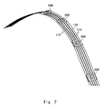
- a wafer 315 to serve as the structure main body 310 of the sensor structure 300 is produced.
- the wafer 315 made of Si is prepared, and its back surface is etched by TMAH (Tetramethyl ammonium hydroxide) to form the recessed portion 314 having a depth of about 10 ⁇ m.
- TMAH Tetramethyl ammonium hydroxide
- the first sensor electrode 320 is formed in the recessed portion 314.
- a mask 317 for allowing an area other than the force transfer portion 311 and the support frame portion 313 to become the thin portion 312 is formed on the surface of the Si wafer 315.
- the mask 317 can be formed by a thermal oxide film.
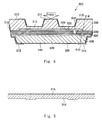
- a wafer in which the signal processing integrated circuit 420 is embedded in the semiconductor substrate 400 is prepared. Then, its surface is covered with the passivation film 430, and the rewiring layer 410 is placed on the passivation film 430. The rewiring layer 410 is connected to an electrode pad 421 of the integrated circuit 420.
- an organic insulating film as the bonding layer 500 is placed on the top surface of the semiconductor substrate 400, and further the second sensor electrode 330 is mounted on the bonding layer 500.
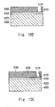
- This process is described with reference to Figs. 10(A) to (H) .
- the semiconductor substrate 400 in which the integrated circuit 420 is embedded is prepared.
- a BCB (Benzocyclobutene) resin film with a thickness of about 10 ⁇ m is formed thereon by spin coating ( Fig. 10A ).
- the BCB (Benzocyclobutene) resin film becomes the bonding layer 500.
- precure is performed for the BCB resin film for one hour in a nitrogen purged oven at 220°C.
- a resist 520 is applied and exposed to light ( Fig. 10B ).
- the resist 520 is cured by post-exposure bake ( Fig. 10C ), and then etched.
- a via (hole) 510 is thereby formed immediately above the rewiring layer 410. ( Fig. 10D ). Then, the semiconductor substrate 400 and the bonding layer 500 are hard-baked.
- the aluminum (Al) is deposited by sputtering on the patterned bonding layer 500 ( Fig. 10E ).
- the aluminum thin film becomes the second sensor electrode 330.
- a resist 520 is applied onto the aluminum thin film and patterned ( Fig. 10F, Fig. 10G ).
- the aluminum is etched ( Fig. 10H ).
- the second sensor electrode 330 is thereby formed at the center excluding the peripheral part, and the second sensor electrode 330 is connected to the rewiring layer 410 of the integrated circuit 420 through the via 510.
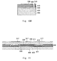
- the wafer 315 ( Fig. 7 ) to become the structure main body 310 and the wafer ( Fig. 9 ) to become the semiconductor substrate 400 are bonded as shown in Fig. 11 .
- a load of 1000N may be applied for one hour at 250°C, for example.
- a protective film 250 for TMAH etching is formed ( Fig. 12 ). It is preferred to use a stack of a photosensitive alkali-resistant organic protective film (ProTEK PSB) on top of a low temperature oxide film deposited by PECVD or sputtering as the protective film 250.
- a silicon thermal oxide film or a silicon nitride film is typically used as a mask material capable of resisting long etching of the Si substrate, those films require high temperature processing (800°C or higher). Such high temperature processing cannot be applied to the semiconductor substrate 400 in which the integrated circuit 420 is embedded. Further, there is a problem that a pin hole occurs when using only a low temperature oxide film, and thus a side etching can occur if only the photosensitive alkali-resistant organic protective film is used.
- the both sides of the bonded wafers are etched ( Fig. 13 ).
- the semiconductor substrate 400 is thereby etched, and the thin portion 312 of the sensor structure 300 is formed at the same time.
- the opening pattern of the protective film 250 is preferably a hole 251 or a single groove 252 as shown in Fig. 14A . If the grooves 252 and 252 cross each other as shown in Fig. 14B , for example, erosion of a corner 254 occurs quickly due to Si crystalline anisotropic etching using an alkaline solution (TMAH), which can cause damage to the integrated circuit 420 inside.
- TMAH alkaline solution
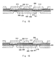
- Etching is stopped when the thickness of about 10 ⁇ m from the electrode pad is left, and the photosensitive alkali-resistant organic protective film 250 is removed ( Fig. 15 ). After that, isotropic etching by XeF 2 gas etching is performed to completely remove the Si substrate ( Fig. 16 ). Then, a BCB resin is deposited as a base insulating film 255 ( Fig. 17 ). After the insulating film is applied, half-dicing is performed from the back surface of the semiconductor substrate using a V-blade ( Fig. 18 ).
- Fig. 18 a cross section along line XVIII-XVIII of Fig. 4 is shown, and it is necessary to lead out the sensor electrodes 320 and 330 from the side surface of the sensor device 200 in this direction. Accordingly, in half-dicing, it is necessary to cut up to the top surface of the bonding layer 500 so as to reach the first sensor electrode 320. One end of the first sensor electrode 320 and the rewiring layer 410 are thereby exposed at the back surface 240 side from the left and right side surfaces.
- wiring lines are formed by shadow masking ( Fig. 20 ).
- a metal material Ti/Cu may be used for example.
- Ti functions as an intermediate layer for enhancing adhesiveness with the insulating film.
- electroless Au plating is performed on the lines to improve the wire bonding property.
- the wafer is divided by dicing, and each of the sensor devices 200 is cut therefrom ( Fig. 21 ).
- the tactile sensor devices 200 can be integrated at the wafer level.
- the tactile sensor devices 200 can be configured as MEMS (Micro Electro Mechanical Systems) that integrally includes the sensor structure 300 and the integrated circuit 420.
- MEMS Micro Electro Mechanical Systems
- the tactile sensor devices 200 can be significantly miniaturized by the integration; for example, one tactile sensor device can be miniaturized to about 3 mm per side.
- the analog sensor signal has a problem that the input impedance is high and the noise is likely to mix in.
- the sensor electrodes 320 and 330 and the integrated circuit 420 are sealed inside the sensor, thereby completely protecting them.
- the second sensor electrode 330 and the integrated circuit 420 are placed in very close proximity to each other with the bonding layer 500 interposed therebetween, the line length between the second sensor electrode 330 and the integrated circuit 420 can be very short.
- the noise is not likely to mix into the analog sensor signals from the sensor electrodes 320 and 330, which allows significant increase in detection accuracy.
- the sensor electrodes 320 and 330 and the integrated circuit 420 are sealed inside the sensor, it is necessary to draw out the electrodes to the outside.
- through-Si-vias through-Si-lines
- the sensor electrodes and the electrodes of the integrated circuit are drawn out by etching and half-dicing from the back side of the semiconductor substrate. It is thus possible to provide external terminals with a small number of steps and without difficulty.
- the first electrode 320 extends to the position reaching the side surface 316 of the structure main body 310 through the back surface of the support frame portion 313, a direct connection can be made to an external power supply or circuit.
- the first electrode 320 is connected to a ground electrode of an external power supply to be at the same voltage, the electrode located closest to the outside serves as the ground, thereby blocking external noise and enhancing the measurement accuracy.
- electrical conduction is established between the first electrode 320 and the structure main body 310, the structure main body 310 is at the ground voltage, the capability to block external noise is further enhanced, and the S/N ratio is improved significantly.
- the electrodes, lines and p-n junction in the sensor electrodes 320 and 330 and the integrated circuit 420 can be protected from corrosion, oxidation, degradation, conductive coating and the like due to the ingress of external moisture, acid, alkalis, organic solvent, oil solution, gas and the like, thereby achieving a stable operation over a long period.
- the device can be thus provided with an organic coating dissolved in an organic solvent or operate under adverse conditions such as muddy water, worn on the hands or feet of the robot.
- the bonding layer 500 is placed on the passivation film 430 at the surface of the signal processing integrated circuit 420 embedded in the semiconductor substrate 400, and the second sensor electrode 330 is formed on top of the bonding layer 500, the length of the wiring line between the capacitor composed of the first sensor electrode 320 and the second sensor electrode 330 and the integrated circuit 420 is short.
- the parasitic capacitance that serves as an important factor to affect the sensitivity and accuracy of the sensors decreases, thus improving the detection sensitivity.
- the wiring length is short, noise is not likely to get mixed.
- the parasitic capacitance between the integrated circuit 420 and the sensor electrode 330 further decreases, so that higher sensitivity can be obtained.
- the inclined surface 211 is at the center of each of the left and right side end surfaces and the inclined surface 221 is at the whole of each of the upper and lower side end surfaces 220, and the metal lead lines 212, 213 and 230 are formed on the respective inclined surfaces.
- the inclined surfaces 211 on the left and right side end surfaces have the shape that is formed only at the center of each of the left and right side end surfaces, which are different from the inclined surfaces on the upper and lower side end surfaces 220. This is made with a view to address issues in fabricating the inclined surfaces; however, the reliability of the lines can be also improved by providing the inclined surface 211 that is slightly recessed than the inclined surface 211.
- the lines for the sensor electrodes 320 and 330 are the lead lines 212 and 213 formed on the inclined surfaces 211 at the left and right side ends, and the lines for the electrodes of the integrated circuit 420 are the lead lines 230, 231, 232 and 234 formed on the inclined surfaces 221 at the upper and lower side ends.
- the depth of wedge cuts to draw out the lines for the sensor electrodes is larger than the depth of wedge cuts to draw out the lines for the integrated circuit. The leading out of the lines in two different directions can be thereby performed stably.
- the bonding layer 500 serves both as an insulating film and an adhesive material.
- the bonding layer 500 needs to have stability as the insulating film and flexibility and adhesiveness as the adhesive material.
- a BCB (Benzocyclobutene) resin film is used as the bonding layer, precure is performed at 220°C, and then the sensor electrodes are patterned. Then, bonding between the sensor structure 300 and the semiconductor substrate 400 is performed at 250°C. At this time, if a procure temperature is set lower, the flexibility and adhesiveness increase but a problem arises in the stability.
- a second embodiment is described hereinbelow.
- the case where the second sensor electrode 330 is formed immediately above the bonding layer 500 placed on the semiconductor substrate 400 and then the structure main body 310 and the semiconductor substrate 400 are bonded together is described by way of illustration.
- a glass substrate 600 on which the second electrode 330 is formed is bonded to the back surface of the structure main body 310, so that the electrodes 320 and 330 of the sensor structure 300 are sealed ( Fig. 22 ). After that, the semiconductor substrate 400 and the wafer of the sensor structure 300 are bonded together by the bonding layer 500.
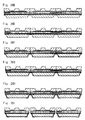
- Figs. 23A to 23I are views showing a fabrication procedure according to the second embodiment.
- the wafer ( Fig. 7 ) to serve as the structure main body 310 and the glass substrate 600 are bonded together.
- the second sensor electrode 330 is formed on the glass substrate 600.
- the first sensor electrode 320 and the second sensor electrode 330 are thereby sealed between the structure main body 310 and the glass substrate 600.
- a groove 318 is made by etching at the position where dicing is to be executed on the side of the second sensor electrode 330 where lead lines are provided. This prevents a dicing blade from cutting to the Si structure main body 310 during half-dicing.
- the bonding layer 500 is formed on the back surface of the glass substrate 600, and the glass substrate 600 and the semiconductor substrate 400 are bonded together.
- Fig. 23G half-dicing for allowing the sensor electrodes 320 and 330 to be exposed outside is executed. At this time, it is necessary to cut up to the top surface of the glass substrate 600.
- the second sensor electrode 330 is formed on the glass substrate 600, and the first sensor electrode 320 and the second sensor electrode 330 are sealed between the structure main body 310 and the glass substrate 600, the shape, gap, and relative position of the first sensor electrode 320 and the second sensor electrode 330 can be set more accurately. It is thereby possible to achieve highly accurate sensor performance.
- a third embodiment is described hereinbelow.
- the case where the glass substrate 600 on which the second electrode 330 is formed is bonded to the back surface of the structure main body 310 to seal the electrodes 320 and 330 of the sensor structure 300, and then the semiconductor substrate 400 and the wafer of the sensor structure 300 are bonded together by the bonding layer 500 is described by way of illustration.
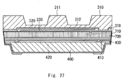
- the third embodiment is characterized in using a LTCC (Low Temperature Co-fired Ceramics) substrate 700 in placed of the glass substrate 600.
- the second sensor electrode 330 is formed on the top surface of the LTCC substrate 700.
- a wiring layer 710 is embedded in the LTCC substrate 700, and the wiring layer 710 is connected to the second sensor electrode 330 through a via 720.
- the lead lines of the second sensor electrode 330 can be led out from the wiring layer 710 of the LTCC substrate 700.
- Figs. 26 are views showing a fabrication procedure according to the third embodiment.
- the wafer ( Fig. 7 ) to serve as the structure main body 310 and the LTCC substrate 700 are bonded together.
- the wiring layer 710 is embedded inside the LTCC substrate 700, and the second sensor electrode 330 formed on the top surface of the LTCC substrate 700 and the wiring layer 710 are connected.
- the first sensor electrode 320 and the second sensor electrode 330 are sealed between the structure main body 310 and the LTCC substrate 700.
- the bonding layer 500 is placed on the back surface of the LTCC substrate 700, and the LTCC substrate 700 and the semiconductor substrate 400 are bonded together.
- Fig. 26G half-dicing for allowing the sensor electrodes 320 and 330 to be exposed outside is executed. At this time, it is necessary to cut up to the top surface of the LTCC substrate 700.
- the second sensor electrode 330 is formed on a ceramic substrate such as the LTCC substrate, for example, the shape, gap, and relative position of the first sensor electrode 320 and the second sensor electrode 330 can be set more accurately just like the case of using the glass substrate 600. Further, because a multilayer interconnection, a capacitor, a coil, an interlayer electrode, an interlayer dielectric film and the like can be formed in the ceramic substrate 700, or passive electronic parts or active electronic parts such as a diode and a transistor can be incorporated between the layers, it is possible to effectively improve the sensor sensitivity or the S/N ratio in an analog manner by analog signal processing before digitization. This significantly increases the functions, varieties and applicable scopes of the sensors.
- Fig. 31 is a cross-sectional view of the sensor device according to the fourth embodiment. As shown in Fig.
- the bonding layer 500 has a via 510 to electrically connect the second sensor electrode 330 and the rewiring layer 410 of the semiconductor substrate 400, and a via 520 to electrically connect the first sensor electrode 320 and the back surface 240.
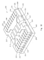
- Fig. 32 is a perspective view of the sensor device according to the fourth embodiment viewed from the back side. As shown in Fig. 32 , the first sensor electrode 320 on the back surface of the structure main body 310 is exposed through the via 520 and led out to the back surface 240 by the lead line 212 connected to the via 520.
- Figs. 33A to 33I are views showing a fabrication process according to the fourth embodiment. As shown in Fig.
- the wafer to serve as the structure main body 310 and the semiconductor substrate 400 on which the bonding layer 500 having the via 520 is formed are first bonded together and thinned ( Fig. 32B ).
- the passivation film 430 is exposed by TMAH wet etching and XeF 2 dry etching ( Fig. 33C ).
- etching is performed to remove the passivation film 430 as shown in Fig. 33D .
- the first and second sensor electrodes 320 and 330 are exposed outside at the same time by the presence of the via 520.
- a photosensitive BCB is deposited to form an insulating film on the back surface 420 of the integrated circuit ( Fig. 33E ).
- RIE Reactive Ion Etching
- the other steps are the same as those of the fabrication process of the first embodiment described above, and the detailed explanation thereof is omitted.
- the sensor structure and the semiconductor substrate are integrated (onto a single chip). In this structure, a sensor signal from the sensor structure 300 can be processed by the integrated circuit 420 embedded in the semiconductor substrate 400. In this manner, by executing signal processing in each of the tactile sensor devices 200, the signal processing load on the information consolidation device 140 can be reduced.
- the diaphragm sensor structure 300 and the LSI in which signal processing units are integrated are bonded by the bonding layer 500 into one integral package as a whole.
- the sensor structure 300 includes two electrode plates 320 and 330 placed opposite to each other. Then, the top surface of the sensor structure 300 functions as the force transfer portion (sensor plane) 311 that comes into contact with an object, and when the force transfer portion 311 is pressed, the distance d between the two electrode plates 320 and 330 changes. A change in capacitance due to the change in the electrode plate distance d is detected as an analog sensor signal.
- the electrode plate distance d changes according to the applied force.
- the charge Q accumulated between the electrode plates changes.
- the charge Q between the electrode plates that changes according to the applied force is transmitted as an analog sensor signal to the integrated circuit 420.
- the charge accumulated in the second sensor electrode 330 is detected by the integrated circuit 420 through the rewiring layer 410 and the electrode pad 421.
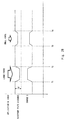
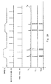
- the integrated circuit 420 converts the analog sensor signal from the sensor structure 300 into digital. The digital conversion of a change in capacitance into a change in frequency is described with reference to Fig. 29 .
- the integrated circuit 420 outputs a selection signal Sct and a reset signal Rst at regular intervals.
- the selection signal Sct is ON signal of a switch (not shown) that is placed between the electrode plate 330 and the integrated circuit 420.
- the reset signal Rst is a signal to reset the charge of the electrode plate 330 to GND.
- the charge Q between the electrode plates is extracted at regular intervals by the selection signal Sct.
- the extracted charge Q between the electrode plates is converted into a voltage V Q through a specified resistor.
- the voltage V Q is compared with a reference voltage Vref.
- a pulse signal Vout having a duration during which V Q exceeds Vref is generated.
- Vout is converted into a pulse signal with a specified frequency by a pulse generator (not shown). By counting the number of pulses per unit time, a force applied to the sensor structure 300 can be measured as a digital quantity.
- the sensor signal digitized by frequency conversion in the above manner is a digital sensor signal.
- the digital sensor signal generated in this manner is transmitted from each of the tactile sensor devices 200 to the information consolidation device 140.
- the signal may be transmitted by differential serial transmission through the two signal lines 113 and 113 of the bus.
- By transmitting the digital signal from the tactile sensor devices 200 to the information consolidation device 140 in this manner it is less likely to be affected by the noise even when the line between the tactile sensor device 200 and the information consolidation device 140 is long.
- the tactile sensor devices 200 are provided on the whole body surface of the robot, the entire line length is considerably long, and therefore noise immunity is important.
- the structure of this embodiment is suitable for the sensor system that includes a large number of tactile sensor devices 200.
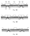
- Figs. 34A to 34D are views showing a fabrication process according to the fifth embodiment. Note that the fabrication process according to the fifth embodiment is applicable to the first to fourth embodiments described above. As shown in Fig.
- the cutting depth is set as a depth enough to reach the structure main body 310 ( Fig. 34B ).
- the support frame portion 313 is cut by half-dicing from the front side ( Fig. 34C ), and element isolation is done naturally ( Fig. 34D ). It is preferred in the half-dicing to perform cutting into the thickness that does not cause the diaphragm performance to vary. This process allows the force transfer portion 311 to be higher than the support frame portion 313 at the same time as element isolation, thereby enhancing the sensitivity to a shearing force and enabling effective detection of a shearing force.
- the structure that facilitates application of a force to the structure main body 310 and brings about accurate deformation of the structure main body 310 by the diaphragm structure composed of the raised force transfer portion 311 and the thin portion 312, and senses the force as a change in the capacitance of the capacitor composed of the first sensor electrode 320 and the second sensor electrode 330 formed internally is described above by way of illustration.
- the structure may be used for the device that applies a pressure to the diaphragm structure composed of the raised force transfer portion 311 and the thin portion 312 and brings about deformation of the structure main body 310, and senses the pressure as a change in the capacitance of the capacitor composed of the first sensor electrode 320 and the second sensor electrode 330 formed internally.
- the deformation of the diaphragm does not concentrate to the center.
- the diaphragm is thereby deformed in a relatively uniform manner, and a large pressure change can be detected with high accuracy.
- the device may be configured such that external heat or heat due to a temperature difference is transferred to the diaphragm structure composed of the raised force transfer portion and the thin portion 312, a shape distortion of the structure main body 310 occurs due to thermal expansion, and a thermal change or a temperature change is sensed as a change in the capacitance of the capacitor composed of the first sensor electrode 320 and the second sensor electrode 330 formed internally.
- a capacitance change due to heat is described in this example, a resistance change due to temperature or a temperature characteristic change at a p-n junction may be detected by the electrode inside the sensor and the signal processing circuit.
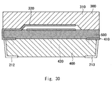
- Fig. 30 is a view showing a structure of the present invention in the simplest manner.
- a sensor structure having a sensor electrode and a semiconductor substrate are bonded by a bonding layer, and the sensor electrode and an external terminal of an integrated circuit are led out to the back surface of the semiconductor substrate through the side surface of the semiconductor substrate.
- the internal sensor electrode can detect a physical quantity such as a pressure, heat or the like applied to the contact sensing surface on the front side.
- the contact sensing surface is not limited to a diaphragm as a matter of course.
- materials of the bonding layer 500, the protective film 250 and the like may be altered as appropriate as a matter of course.
Landscapes
- Engineering & Computer Science (AREA)
- Physics & Mathematics (AREA)
- General Physics & Mathematics (AREA)
- Manufacturing & Machinery (AREA)
- Power Engineering (AREA)
- Microelectronics & Electronic Packaging (AREA)
- Chemical & Material Sciences (AREA)
- Analytical Chemistry (AREA)
- Robotics (AREA)
- Mechanical Engineering (AREA)
- Pressure Sensors (AREA)
Abstract
Provided is a technique for packaging a sensor structure (300) having a contact sensing surface and a signal processing LSI (420) that processes a sensor signal. The sensor structure (300) has the contact sensing surface and sensor electrodes (320, 330). The signal processing integrated circuit (420) is embedded in a semiconductor substrate (400). The sensor structure (300) and the semiconductor substrate (400) are bonded by a bonding layer (500), forming a sensor device (200) as a single chip. The sensor electrodes (320, 330) and the integrated circuit (420) are sealed inside the sensor device (200), and the sensor electrodes (320, 330) and external terminals of the integrated circuit (420) are led out to the back surface of the semiconductor substrate (400) through a side surface of the semiconductor substrate (400).
Description
- The present invention relates to a sensor device and a method for fabricating a sensor device.
- Currently the development of humanoid robots is making progress.
For humanoid robots, advanced motions such as contacting with people, autonomously bypassing an obstruction and grasping and moving an object are required.
Because a tactile sense is required to achieve such motions, studies to provide the hands or the whole surface of a robot with a tactile sensor are under way (for example, seePatent Literature 1 to Patent Literature 6). - Existing tactile sensor systems typically have a mesh structure.
For example, a plurality of electrode lines are formed on each of two electrode sheets.
The electrode sheets are then placed opposite to each other in such a way that their electrode lines are orthogonal to each other, thereby forming mesh wiring lines.
A pressure-sensitive conductive member is interposed between the two electrode sheets, or a tactile sensor element is mounted at each intersection of the electrode lines.
Each tactile sensor element converts a pressure change or a temperature change due to contact with an object into an electrical signal change according to the amount of change. - A control unit is connected to each of the electrode lines and makes central control of a plurality of tactile sensor elements. Specifically, the control unit sequentially selects the tactile sensor elements and performs sampling of sensor values of the respective sensors. The control unit accumulates electrical signals from the tactile sensor elements and makes data processing.
By repeating such a sampling operation on a regular basis, whether a robot is in contact with an object and further which sensor is in contact are sensed.
It is thereby possible to sense in which position and with what strength the robot is in contact with the object. -
- [PTL 1] Japanese Unexamined Patent Application Publication No.
2006-337315 - [PTL 2] Japanese Unexamined Patent Application Publication No.
2007-10482 - [PTL 3] Japanese Unexamined Patent Application Publication No.
2007-285784 - [PTL 4] Japanese Unexamined Patent Application Publication No.
2007-78382 - [PTL 5] Japanese Unexamined Patent Application Publication No.
2006-287520 - [PTL 6] Japanese Unexamined Patent Application Publication No.
2006-281347 - [PTL 7] Japanese Patent No.
03621093 - The existing tactile sensor systems have the following problems.
In the technology disclosed inPatent Literature 1 to Patent Literature 6, the control unit, acting as a host, manages a large number of tactile sensor elements in a concentrated manner, sequentially selects the tactile sensor elements, and performs sampling of sensor values of the respective sensors.
In this structure, there is a problem that the processing load on the control unit becomes excessive with an increase in the number of sensors.
Further, the sampling interval becomes large with an increase in the number of sensors. This inevitably causes a decrease in the response speed to become slow to respond, which is a critical problem for the tactile sensor system of a robot. - Further, when thought is given to placing a large number of tactile sensors on the whole body surface of a robot, the number of lines between the tactile sensors and the control unit is enormous.
Thus, it is practically very difficult to mount a large number of tactile sensors at desired positions, and its maintenance and failure repair are extremely difficult.
Furthermore, because the lines between the tactile sensors and the control unit are long, a sensor signal is likely to be degraded due to noise. - In light of the above, one approach is to incorporate a sensor structure and a signal processing unit into each single tactile sensor.
Then, the signal processing unit can sense and amplify a sensor signal from the sensor structure and further perform digital processing. - To achieve this, technology to integrate the sensor structure and the signal processing unit is required.
For example, packaging technology called Shell Case is disclosed in Japanese Patent No.03621093
In Japanese Patent No.03621093
In this structure, a plurality of wafers can be bonded together, and the device chip is securely protected with the glass plates.
However, according to the technology of Japanese Patent No.03621093 - In view of the above circumstances, technology to incorporate a sensor structure having a contact sensing surface and a signal processing LSI that processes a sensor signal into package is desired.
- A sensor device according to the present invention includes a sensor structure including a contact sensing surface that comes into direct contact with a detection target on one surface exposed outside and a sensor electrode that outputs an analog sensor signal upon sensing a change in the contact sensing surface at another surface side on an opposite side of the contact sensing surface, a semiconductor substrate including an embedded signal processing integrated circuit that processes the analog sensor signal, and a bonding layer interposed between said another surface of the sensor structure and the semiconductor substrate to bond the sensor structure and the semiconductor substrate together, wherein the sensor structure and the semiconductor substrate are stacked into a single chip with the sensor electrode and the integrated circuit placed opposite to each other with the bonding layer interposed therebetween, the sensor electrode and the integrated circuit are sealed inside the sensor device, and the sensor electrode and at least any of external terminals of the signal processing integrated circuit are led out to a back surface of the semiconductor substrate through a side surface of the semiconductor substrate.
- A method for fabricating a sensor device according to the present invention includes placing a sensor electrode on a back surface of a wafer to serve as a sensor structure, producing a semiconductor substrate with an embedded signal processing integrated circuit, bonding the sensor structure and the semiconductor substrate together by a bonding layer with the sensor electrode and the integrated circuit placed opposite to each other, etching a back surface of the semiconductor substrate and performing half-dicing of the semiconductor substrate from the back surface to make a line draw-out portion of the sensor electrode and an electrode draw-out portion of the integrated circuit exposed at a back side of the semiconductor substrate, placing a lead line from an inclined surface to the back surface of the semiconductor substrate formed by the etching and the half-dicing, and leading out the sensor electrode and an external terminal of the signal processing integrated circuit to the back surface of the semiconductor substrate through a side surface of the semiconductor substrate.
-
-
Fig. 1 is a view showing a tactile sensor system applied to a robot hand; -
Fig. 2 is a view showing a plurality of sensor devices mounted on a bus; -
Fig. 3 is a perspective view of a sensor device viewed from the front side; -
Fig. 4 is a perspective view of a sensor device viewed from the back side; -
Fig. 5 is a cross-sectional view of a sensor device; -
Fig. 6 is a view showing a fabrication process for a sensor device according to a first embodiment; -
Fig. 7 is a view showing a fabrication process for a sensor device according to the first embodiment; -
Fig. 8 is a view showing a fabrication process for a sensor device according to the first embodiment; -
Fig. 9 is a view showing a fabrication process for a sensor device according to the first embodiment; -
Fig. 10A is a view showing a fabrication process for a sensor device according to the first embodiment; -
Fig. 10B is a view showing a fabrication process for a sensor device according to the first embodiment; -
Fig. 10C is a view showing a fabrication process for a sensor device according to the first embodiment; -
Fig. 10D is a view showing a fabrication process for a sensor device according to the first embodiment; -
Fig. 10E is a view showing a fabrication process for a sensor device according to the first embodiment; -
Fig. 10F is a view showing a fabrication process for a sensor device according to the first embodiment; -
Fig. 10G is a view showing a fabrication process for a sensor device according to the first embodiment; -
Fig. 10H is a view showing a fabrication process for a sensor device according to the first embodiment; -
Fig. 11 is a view showing a fabrication process for a sensor device according to the first embodiment; -
Fig. 12 is a view showing a fabrication process for a sensor device according to the first embodiment; -
Fig. 13 is a view showing a fabrication process for a sensor device according to the first embodiment; -
Fig. 14A is a view showing an opening pattern of a protective film; -
Fig. 14B is a view to explain a drawback when grooves cross each other; -
Fig. 15 is a view showing a fabrication process for a sensor device according to the first embodiment; -
Fig. 16 is a view showing a fabrication process for a sensor device according to the first embodiment; -
Fig. 17 is a view showing a fabrication process for a sensor device according to the first embodiment; -
Fig. 18 is a view showing a fabrication process for a sensor device according to the first embodiment; -
Fig. 19 is a view showing a fabrication process for a sensor device according to the first embodiment; -
Fig. 20 is a view showing a fabrication process for a sensor device according to the first embodiment; -
Fig. 21 is a view showing a fabrication process for a sensor device according to the first embodiment; -
Fig. 22 is a view showing a structure of a second embodiment in an exploded fashion; -
Fig. 23A is a view showing a fabrication process according to the second embodiment; -
Fig. 23B is a view showing a fabrication process according to the second embodiment; -
Fig. 23C is a view showing a fabrication process according to the second embodiment; -
Fig. 23D is a view showing a fabrication process according to the second embodiment; -
Fig. 23E is a view showing a fabrication process according to the second embodiment; -
Fig. 23F is a view showing a fabrication process according to the second embodiment; -
Fig. 23G is a view showing a fabrication process according to the second embodiment; -
Fig. 23H is a view showing a fabrication process according to the second embodiment; -
Fig. 23I is a view showing a fabrication process according to the second embodiment; -
Fig. 24 is a view showing a structure of the second embodiment; -
Fig. 25 is a view showing a structure of a third embodiment in an exploded fashion; -
Fig. 26A is a view showing a fabrication process according to the third embodiment; -
Fig. 26B is a view showing a fabrication process according to the third embodiment; -
Fig. 26C is a view showing a fabrication process according to the third embodiment; -
Fig. 26D is a view showing a fabrication process according to the third embodiment; -
Fig. 26E is a view showing a fabrication process according to the third embodiment; -
Fig. 26F is a view showing a fabrication process according to the third embodiment; -
Fig. 26G is a view showing a fabrication process according to the third embodiment; -
Fig. 26H is a view showing a fabrication process according to the third embodiment; -
Fig. 26I is a view showing a fabrication process according to the third embodiment; -
Fig. 27 is a view showing a structure of the third embodiment; -
Fig. 28 is a view to explain a procedure to convert a sensor signal into a digital signal; -
Fig. 29 is a view to explain a procedure to convert a sensor signal into a digital signal; -
Fig. 30 is a view showing a structure of the present invention in the simplest manner; -
Fig. 31 is a cross-sectional view of a sensor device according to a fourth embodiment; -
Fig. 32 is a perspective view of a sensor device according to the fourth embodiment viewed from the back side; -
Fig. 33A is a view showing a fabrication process according to the fourth embodiment; -
Fig. 33B is a view showing a fabrication process according to the fourth embodiment; -
Fig. 33C is a view showing a fabrication process according to the fourth embodiment; -
Fig. 33D is a view showing a fabrication process according to the fourth embodiment; -
Fig. 33E is a view showing a fabrication process according to the fourth embodiment; -
Fig. 33F is a view showing a fabrication process according to the fourth embodiment; -
Fig. 33G is a view showing a fabrication process according to the fourth embodiment; -
Fig. 33H is a view showing a fabrication process according to the fourth embodiment; -
Fig. 33I is a view showing a fabrication process according to the fourth embodiment; -
Fig. 34A is a view showing a fabrication process according to a fifth embodiment; -
Fig. 34B is a view showing a fabrication process according to the fifth embodiment; -
Fig. 34C is a view showing a fabrication process according to the fifth embodiment; and -
Fig. 34D is a view showing a fabrication process according to the fifth embodiment. - Embodiments of the present invention are illustrated in drawings and described with reference to the reference numerals assigned to elements in the drawings.
- A first embodiment of the sensor device according to the present invention is described hereinbelow.
Fig. 1 is a view showing the way a tactile sensor system in which a large number of sensor devices are mounted is applied to a robot hand.
Fig. 2 is a view showing the way a plurality ofsensor devices 200 are mounted on abus 110. - Sensor devices according to this embodiment are mounted on a
hand 11 of arobot 10 as shown inFig. 1 or on the whole body surface of a robot, thereby constituting atactile sensor system 100 as a whole.
A plurality oftactile sensor devices 200 are mounted on eachbus 110.
In this embodiment, fourlines bus 110.
Two of the four lines arepower supply lines signal lines
Then, allbuses 110 are connected to aninformation consolidation device 140 through aninformation relay device 120 and aline concentration device 130. - When the
hand 11 of therobot 10 grasps an object (not shown), for example, and the surface of therobot 10 comes into contact with the object, each of thesensor devices 200 senses a contact pressure.
Further, each of thesensor devices 200 executes digital signal processing of a sensor signal.
Then, the digital-processed sensor signal is transmitted from each of thesensor devices 200 to theinformation consolidation device 140.
Theinformation consolidation device 140 consolidates the information from thesensor devices 200 and detects how much force is exerted on which position. - A structure of the sensor device is described hereinbelow.
Fig. 3 is a perspective view of the sensor device viewed from the front side.
Fig. 4 is a perspective view of the sensor device viewed from the back side.
Fig. 5 is a cross-sectional view of the sensor device. - As shown in
Fig. 5 , thesensor device 200 has a structure in which asensor structure 300 and asemiconductor substrate 400 are bonded together by abonding layer 500.
Thesensor structure 300 includes a structuremain body 310, afirst sensor electrode 320, and asecond sensor electrode 330.
The structuremain body 310 is made of Si. - When viewed from the front side, a raised
force transfer portion 311 that comes into contact with an object is placed at the center of the structuremain body 310, and theforce transfer portion 311 is surrounded by a recessedthin portion 312.
Thethin portion 312 is elastic, so that the structuremain body 310 functions as a working film. Specifically, the structuremain body 310 bends when a force acts on theforce transfer portion 311. - The
force transfer portion 311 forms a contact sensing surface. - The edge on the periphery of the
thin portion 312 is asupport frame portion 313 that supports the working film.
Further, a recessedportion 314 is formed on the back surface of the structuremain body 310. - The
first sensor electrode 320 is mounted on the recessedportion 314 that is formed on the back surface of the structuremain body 310.
At least one end of thefirst sensor electrode 320 extends to the position reaching aside surface 316 of the structuremain body 310 through the back surface of thesupport frame portion 313.
Thefirst sensor electrode 320 is a movable electrode that is displaced together with the working film. - The
second sensor electrode 330 is mounted immediately above thebonding layer 500.
The distance between thefirst sensor electrode 320 and thesecond sensor electrode 330 is determined by the depth of the recessedportion 314.
Thesecond sensor electrode 330 is a fixed electrode, and thefirst sensor electrode 320 and thesecond sensor electrode 330 placed opposite to each other constitute a capacitor.
Thesecond sensor electrode 330 is connected to arewiring layer 410 of thesemiconductor substrate 400 through a via 510 in thebonding layer 500. - A signal processing integrated
circuit 420 is embedded in thesemiconductor substrate 400, and its surface is covered with apassivation film 430.
Further, therewiring layer 410 is placed on thepassivation film 430.
Thebonding layer 500 is placed immediately above thesemiconductor substrate 400, and thesecond sensor electrode 330 and theintegrated circuit 420 is placed opposite to each other with thebonding layer 500 interposed therebetween.
Further, the first andsecond sensor electrodes integrated circuit 420 are sealed inside thesensor device 200. - The
bonding layer 500 preferably has a thickness of 10 µm or more to reduce the parasitic capacitance between theintegrated circuit 420 and thesensor electrode 330.
Although the upper limit of the thickness is not particularly set, the thickness may be up to 100 µm, for example, taking the convenience of fabrication of a semiconductor chip or the like into account. - When the
sensor device 200 is viewed from the back side, aninclined surface 211 is formed at the center of each of the side end surfaces in the horizontal direction ofFig. 4 .
Then,metal lead lines inclined surfaces 211, and thelead lines back surface 240.
Onelead line 212 is connected to one end of thefirst sensor electrode 320, and the otherlead line 213 is connected to thesecond sensor electrode 330 through the rewiring layer 410 (seeFig. 5 ). - Further, side end surfaces 220 and 220 in the vertical direction of
Fig. 4 are entirely formed asinclined surfaces lead lines 230 each are mounted to reach theback surface 240 on each of the side end surfaces 220 and 220.
The lead lines 230 are led out from therewiring layer 410 and serve as power supply lines or signal lines of theintegrated circuit 420. - On the
back surface 240 of thesensor device 200 shown inFig. 4 , external connection terminals are mounted.
In this embodiment, fourexternal terminals 241 to 244, corresponding to fourwiring lines bus 110, are mounted on the back surface of thesensor device 200.
InFig. 4 , a firstexternal terminal 241, a secondexternal terminal 242, a thirdexternal terminal 243 and a fourthexternal terminal 244 are shown sequentially from the left. - The first
external terminal 241 is an external terminal that is connected to GND of thebus 110, for example, and thelead line 212 from aleft side surface 210 and alead line 231 at the leftmost of alower side surface 220 are connected to the firstexternal terminal 241.
Alead line 232 at the leftmost of anupper side surface 220 is connected to the secondexternal terminal 242, and alead line 234 at the rightmost of thelower side surface 220 is connected to the thirdexternal terminal 243.
Thelead line 213 from aright side surface 210 and alead line 234 at the rightmost of theupper side surface 220 are connected to the fourthexternal terminal 244. - Note that the number of
external terminals 241 to 244 is varied as appropriate according to the number of signal lines, and connections between the lead lines and the external terminals may be varied as appropriate according to the structure of thesensor structure 300 and theintegrated circuit 420 as a matter of course. - A fabrication method for a sensor device is described hereinbelow.
Figs. 6 to 21 are views showing a fabrication procedure for a sensor device.
First, awafer 315 to serve as the structuremain body 310 of thesensor structure 300 is produced.
Specifically, as shown inFig. 6 , thewafer 315 made of Si is prepared, and its back surface is etched by TMAH (Tetramethyl ammonium hydroxide) to form the recessedportion 314 having a depth of about 10 µm. Then, as shown inFig. 7 , thefirst sensor electrode 320 is formed in the recessedportion 314. Further, on the surface of theSi wafer 315, amask 317 for allowing an area other than theforce transfer portion 311 and thesupport frame portion 313 to become thethin portion 312 is formed.
Themask 317 can be formed by a thermal oxide film. - Further, on the other hand, as shown in
Fig. 8 , a wafer in which the signal processing integratedcircuit 420 is embedded in thesemiconductor substrate 400 is prepared.
Then, its surface is covered with thepassivation film 430, and therewiring layer 410 is placed on thepassivation film 430.
Therewiring layer 410 is connected to anelectrode pad 421 of theintegrated circuit 420. - Next, as shown in
Fig. 9 , an organic insulating film as thebonding layer 500 is placed on the top surface of thesemiconductor substrate 400, and further thesecond sensor electrode 330 is mounted on thebonding layer 500.
This process is described with reference toFigs. 10(A) to (H) .
As mentioned above, thesemiconductor substrate 400 in which theintegrated circuit 420 is embedded is prepared.
A BCB (Benzocyclobutene) resin film with a thickness of about 10 µm is formed thereon by spin coating (Fig. 10A ).
The BCB (Benzocyclobutene) resin film becomes thebonding layer 500.
Then, precure is performed for the BCB resin film for one hour in a nitrogen purged oven at 220°C. - On the BCB film, a resist 520 is applied and exposed to light (
Fig. 10B ).
The resist 520 is cured by post-exposure bake (Fig. 10C ), and then etched.
A via (hole) 510 is thereby formed immediately above therewiring layer 410. (Fig. 10D ).
Then, thesemiconductor substrate 400 and thebonding layer 500 are hard-baked. - After that, aluminum (Al) is deposited by sputtering on the patterned bonding layer 500 (
Fig. 10E ).
The aluminum thin film becomes thesecond sensor electrode 330.
A resist 520 is applied onto the aluminum thin film and patterned (Fig. 10F, Fig. 10G ).
Then, the aluminum is etched (Fig. 10H ).
Thesecond sensor electrode 330 is thereby formed at the center excluding the peripheral part, and thesecond sensor electrode 330 is connected to therewiring layer 410 of theintegrated circuit 420 through thevia 510. - Then, the wafer 315 (
Fig. 7 ) to become the structuremain body 310 and the wafer (Fig. 9 ) to become thesemiconductor substrate 400 are bonded as shown inFig. 11 .
For the bonding, a load of 1000N may be applied for one hour at 250°C, for example. - On the back surface of the
semiconductor substrate 400, aprotective film 250 for TMAH etching is formed (Fig. 12 ).
It is preferred to use a stack of a photosensitive alkali-resistant organic protective film (ProTEK PSB) on top of a low temperature oxide film deposited by PECVD or sputtering as theprotective film 250.
Although a silicon thermal oxide film or a silicon nitride film is typically used as a mask material capable of resisting long etching of the Si substrate, those films require high temperature processing (800°C or higher).
Such high temperature processing cannot be applied to thesemiconductor substrate 400 in which theintegrated circuit 420 is embedded.
Further, there is a problem that a pin hole occurs when using only a low temperature oxide film, and thus a side etching can occur if only the photosensitive alkali-resistant organic protective film is used. - After forming the
protective film 250, the both sides of the bonded wafers are etched (Fig. 13 ).
Thesemiconductor substrate 400 is thereby etched, and thethin portion 312 of thesensor structure 300 is formed at the same time. - Note that the opening pattern of the
protective film 250 is preferably ahole 251 or asingle groove 252 as shown inFig. 14A .
If thegrooves Fig. 14B , for example, erosion of acorner 254 occurs quickly due to Si crystalline anisotropic etching using an alkaline solution (TMAH), which can cause damage to theintegrated circuit 420 inside. - Etching is stopped when the thickness of about 10 µm from the electrode pad is left, and the photosensitive alkali-resistant organic
protective film 250 is removed (Fig. 15 ).
After that, isotropic etching by XeF2 gas etching is performed to completely remove the Si substrate (Fig. 16 ).
Then, a BCB resin is deposited as a base insulating film 255 (Fig. 17 ).
After the insulating film is applied, half-dicing is performed from the back surface of the semiconductor substrate using a V-blade (Fig. 18 ). - In
Fig. 18 , a cross section along line XVIII-XVIII ofFig. 4 is shown, and it is necessary to lead out thesensor electrodes sensor device 200 in this direction.
Accordingly, in half-dicing, it is necessary to cut up to the top surface of thebonding layer 500 so as to reach thefirst sensor electrode 320.
One end of thefirst sensor electrode 320 and therewiring layer 410 are thereby exposed at theback surface 240 side from the left and right side surfaces. - On the other hand, in the direction of a cross section along line XIX-XIX in
Fig. 4 , it is only necessary to lead out theelectrode pad 421 of theintegrated circuit 420, and therefore shallow half-dicing that reaches theelectrode pad 421 or therewiring layer 410 is enough as shown inFig. 19 . - Then, wiring lines are formed by shadow masking (
Fig. 20 ).
As a metal material, Ti/Cu may be used for example.
Ti functions as an intermediate layer for enhancing adhesiveness with the insulating film.
After that, electroless Au plating is performed on the lines to improve the wire bonding property.
Finally, the wafer is divided by dicing, and each of thesensor devices 200 is cut therefrom (Fig. 21 ). - The following advantages are obtained by the first embodiment. (1) By the fabrication method according to this embodiment, the
tactile sensor devices 200 can be integrated at the wafer level.
In other words, thetactile sensor devices 200 can be configured as MEMS (Micro Electro Mechanical Systems) that integrally includes thesensor structure 300 and theintegrated circuit 420.
Further, thetactile sensor devices 200 can be significantly miniaturized by the integration; for example, one tactile sensor device can be miniaturized to about 3 mm per side.
By producing MEMS that integrally includes thesensor structure 300 and theintegrated circuit 420 and achieving militarization, it becomes suitable as a sensor system that is mounted on the body surface of therobot 10, for example. - (2) Although the accumulated electrical charge is read as an analog sensor signal from the
sensor electrodes integrated circuit 420, the analog sensor signal has a problem that the input impedance is high and the noise is likely to mix in.
With regard to this point, in this embodiment, thesensor electrodes integrated circuit 420 are sealed inside the sensor, thereby completely protecting them.
Further, because thesecond sensor electrode 330 and theintegrated circuit 420 are placed in very close proximity to each other with thebonding layer 500 interposed therebetween, the line length between thesecond sensor electrode 330 and theintegrated circuit 420 can be very short. Thus, the noise is not likely to mix into the analog sensor signals from thesensor electrodes - (3) In the fabrication method according to this embodiment, because the
sensor structure 300 and thesemiconductor substrate 400 are bonded together by thebonding layer 500, no limitations are imposed on the structure of theintegrated circuit 420 that is embedded in thesemiconductor substrate 400.
For example, thesemiconductor substrate 400 in which the existing sense amplifier and signal processing circuit are embedded may be applied to this embodiment. - (4) In this embodiment, because the
sensor electrodes integrated circuit 420 are sealed inside the sensor, it is necessary to draw out the electrodes to the outside.
To draw out the electrodes to the outside from the chip sealed inside the package, through-Si-vias (through-Si-lines) could be formed; however, providing the through-Si-vias of the same number as the number of wiring lines required causes a significant increase in the number of steps and the difficulty of processing.
With regard to this point, in this embodiment, the sensor electrodes and the electrodes of the integrated circuit are drawn out by etching and half-dicing from the back side of the semiconductor substrate.
It is thus possible to provide external terminals with a small number of steps and without difficulty. - (5) By diaphragm structure composed of the
force transfer portion 311 and thethin portion 312, a force applied to the structuremain body 310 is correctly reflected in the deformation of the structuremain body 310.
Further, because thefirst sensor electrode 320 is formed directly on the back surface of the structuremain body 310, the deformation of the structuremain body 310 due to the external force received by theforce transfer portion 311 can be converted into the displacement of thefirst sensor electrode 320, and the applied force can be sensed with high accuracy as a change in the capacitance of the capacitor formed together with thesecond sensor electrode 330. - (6) Because at least one end of the
first electrode 320 extends to the position reaching theside surface 316 of the structuremain body 310 through the back surface of thesupport frame portion 313, a direct connection can be made to an external power supply or circuit.
For example, if thefirst electrode 320 is connected to a ground electrode of an external power supply to be at the same voltage, the electrode located closest to the outside serves as the ground, thereby blocking external noise and enhancing the measurement accuracy.
Further, if electrical conduction is established between thefirst electrode 320 and the structuremain body 310, the structuremain body 310 is at the ground voltage, the capability to block external noise is further enhanced, and the S/N ratio is improved significantly. - (7) Because the first and
second sensor electrodes integrated circuit 420 are sealed inside thesensor device 200, the electrodes, lines and p-n junction in thesensor electrodes integrated circuit 420 can be protected from corrosion, oxidation, degradation, conductive coating and the like due to the ingress of external moisture, acid, alkalis, organic solvent, oil solution, gas and the like, thereby achieving a stable operation over a long period.
The device can be thus provided with an organic coating dissolved in an organic solvent or operate under adverse conditions such as muddy water, worn on the hands or feet of the robot. - (8) Because the
bonding layer 500 is placed on thepassivation film 430 at the surface of the signal processing integratedcircuit 420 embedded in thesemiconductor substrate 400, and thesecond sensor electrode 330 is formed on top of thebonding layer 500, the length of the wiring line between the capacitor composed of thefirst sensor electrode 320 and thesecond sensor electrode 330 and theintegrated circuit 420 is short.
Thus, the parasitic capacitance that serves as an important factor to affect the sensitivity and accuracy of the sensors decreases, thus improving the detection sensitivity.
Because the wiring length is short, noise is not likely to get mixed.
By increasing the thickness of thebonding layer 500, the parasitic capacitance between theintegrated circuit 420 and thesensor electrode 330 further decreases, so that higher sensitivity can be obtained. - (9) The
inclined surface 211 is at the center of each of the left and right side end surfaces and theinclined surface 221 is at the whole of each of the upper and lower side end surfaces 220, and themetal lead lines lines
By these shape and structure, stability to temperature and durability against repeated temperature change increase, and therefore the reliability of the lines upon mounting of the devices or during use is significantly improved.
The inclined surfaces 211 on the left and right side end surfaces have the shape that is formed only at the center of each of the left and right side end surfaces, which are different from the inclined surfaces on the upper and lower side end surfaces 220.
This is made with a view to address issues in fabricating the inclined surfaces; however, the reliability of the lines can be also improved by providing theinclined surface 211 that is slightly recessed than theinclined surface 211. - (10) The lines for the
sensor electrodes lead lines inclined surfaces 211 at the left and right side ends, and the lines for the electrodes of theintegrated circuit 420 are thelead lines inclined surfaces 221 at the upper and lower side ends.
The depth of wedge cuts to draw out the lines for the sensor electrodes is larger than the depth of wedge cuts to draw out the lines for the integrated circuit.
The leading out of the lines in two different directions can be thereby performed stably. - (11) In this embodiment, the
bonding layer 500 serves both as an insulating film and an adhesive material.
Thus, thebonding layer 500 needs to have stability as the insulating film and flexibility and adhesiveness as the adhesive material.
With regard to this point, in this embodiment, a BCB (Benzocyclobutene) resin film is used as the bonding layer, precure is performed at 220°C, and then the sensor electrodes are patterned.
Then, bonding between thesensor structure 300 and thesemiconductor substrate 400 is performed at 250°C.
At this time, if a procure temperature is set lower, the flexibility and adhesiveness increase but a problem arises in the stability.
On the other hand, if a procure temperature is set higher, the stability increases but the adhesiveness and flexibility cannot be maintained, and, if a junction temperature is set higher to compensate for this, damage occurs to the sensor electrodes.
In this embodiment, those issues can be overcome, and the most suitable stability, flexibility and adhesiveness can be achieved. - A second embodiment is described hereinbelow.
In the first embodiment, the case where thesecond sensor electrode 330 is formed immediately above thebonding layer 500 placed on thesemiconductor substrate 400 and then the structuremain body 310 and thesemiconductor substrate 400 are bonded together is described by way of illustration.
On the other hand, in the second embodiment, aglass substrate 600 on which thesecond electrode 330 is formed is bonded to the back surface of the structuremain body 310, so that theelectrodes sensor structure 300 are sealed (Fig. 22 ).
After that, thesemiconductor substrate 400 and the wafer of thesensor structure 300 are bonded together by thebonding layer 500. -
Figs. 23A to 23I are views showing a fabrication procedure according to the second embodiment.
As shown inFig. 23A , the wafer (Fig. 7 ) to serve as the structuremain body 310 and theglass substrate 600 are bonded together.
At this time, thesecond sensor electrode 330 is formed on theglass substrate 600.
Thefirst sensor electrode 320 and thesecond sensor electrode 330 are thereby sealed between the structuremain body 310 and theglass substrate 600. - Note that, in
Fig. 23A , in the wafer to serve as the structuremain body 310, agroove 318 is made by etching at the position where dicing is to be executed on the side of thesecond sensor electrode 330 where lead lines are provided.
This prevents a dicing blade from cutting to the Si structuremain body 310 during half-dicing. - Then, the
bonding layer 500 is formed on the back surface of theglass substrate 600, and theglass substrate 600 and thesemiconductor substrate 400 are bonded together. - In
Fig. 23G , half-dicing for allowing thesensor electrodes
At this time, it is necessary to cut up to the top surface of theglass substrate 600. - The other procedural steps are the same as those described in the first embodiment, and the sensor device shown in
Fig. 24 is obtained finally. - In this structure, because the wafer (
Fig. 7 ) to serve as the structuremain body 310 and theglass substrate 600 are bonded together, thesecond sensor electrode 330 is formed on theglass substrate 600, and thefirst sensor electrode 320 and thesecond sensor electrode 330 are sealed between the structuremain body 310 and theglass substrate 600, the shape, gap, and relative position of thefirst sensor electrode 320 and thesecond sensor electrode 330 can be set more accurately.
It is thereby possible to achieve highly accurate sensor performance. - A third embodiment is described hereinbelow.
In the above second embodiment, the case where theglass substrate 600 on which thesecond electrode 330 is formed is bonded to the back surface of the structuremain body 310 to seal theelectrodes sensor structure 300, and then thesemiconductor substrate 400 and the wafer of thesensor structure 300 are bonded together by thebonding layer 500 is described by way of illustration.
With regard to this point, the third embodiment is characterized in using a LTCC (Low Temperature Co-fired Ceramics)substrate 700 in placed of theglass substrate 600.
InFig. 25 , thesecond sensor electrode 330 is formed on the top surface of theLTCC substrate 700.
Further, awiring layer 710 is embedded in theLTCC substrate 700, and thewiring layer 710 is connected to thesecond sensor electrode 330 through a via 720.
Thus, the lead lines of thesecond sensor electrode 330 can be led out from thewiring layer 710 of theLTCC substrate 700. -
Figs. 26 are views showing a fabrication procedure according to the third embodiment.
As shown inFig. 26A , the wafer (Fig. 7 ) to serve as the structuremain body 310 and theLTCC substrate 700 are bonded together.
At this time, thewiring layer 710 is embedded inside theLTCC substrate 700, and thesecond sensor electrode 330 formed on the top surface of theLTCC substrate 700 and thewiring layer 710 are connected.
At the stage ofFig. 26A , thefirst sensor electrode 320 and thesecond sensor electrode 330 are sealed between the structuremain body 310 and theLTCC substrate 700. - Then, the
bonding layer 500 is placed on the back surface of theLTCC substrate 700, and theLTCC substrate 700 and thesemiconductor substrate 400 are bonded together. - In
Fig. 26G , half-dicing for allowing thesensor electrodes
At this time, it is necessary to cut up to the top surface of theLTCC substrate 700. - The other procedural steps are the same as those described in the first embodiment, and the sensor device shown in
Fig. 27 is obtained finally. - Because the
second sensor electrode 330 is formed on a ceramic substrate such as the LTCC substrate, for example, the shape, gap, and relative position of thefirst sensor electrode 320 and thesecond sensor electrode 330 can be set more accurately just like the case of using theglass substrate 600.
Further, because a multilayer interconnection, a capacitor, a coil, an interlayer electrode, an interlayer dielectric film and the like can be formed in theceramic substrate 700, or passive electronic parts or active electronic parts such as a diode and a transistor can be incorporated between the layers, it is possible to effectively improve the sensor sensitivity or the S/N ratio in an analog manner by analog signal processing before digitization.
This significantly increases the functions, varieties and applicable scopes of the sensors. - Although the first and
second sensor electrodes second sensor electrodes
Fig. 31 is a cross-sectional view of the sensor device according to the fourth embodiment. As shown inFig. 31 , thebonding layer 500 has a via 510 to electrically connect thesecond sensor electrode 330 and therewiring layer 410 of thesemiconductor substrate 400, and a via 520 to electrically connect thefirst sensor electrode 320 and theback surface 240.
Fig. 32 is a perspective view of the sensor device according to the fourth embodiment viewed from the back side. As shown inFig. 32 , thefirst sensor electrode 320 on the back surface of the structuremain body 310 is exposed through the via 520 and led out to theback surface 240 by thelead line 212 connected to thevia 520.
Figs. 33A to 33I are views showing a fabrication process according to the fourth embodiment. As shown inFig. 32A , the wafer to serve as the structuremain body 310 and thesemiconductor substrate 400 on which thebonding layer 500 having the via 520 is formed are first bonded together and thinned (Fig. 32B ).
Next, thepassivation film 430 is exposed by TMAH wet etching and XeF2 dry etching (Fig. 33C ). After that, etching is performed to remove thepassivation film 430 as shown inFig. 33D . As a result, the first andsecond sensor electrodes via 520.
Further, a photosensitive BCB is deposited to form an insulating film on theback surface 420 of the integrated circuit (Fig. 33E ). RIE (Reactive Ion Etching) is performed on the deposited BCB, and the first andsecond sensor electrodes Figs. 33F ).
Note that, in the fabrication process according to the fourth embodiment, the other steps are the same as those of the fabrication process of the first embodiment described above, and the detailed explanation thereof is omitted.
Further, in the first to fourth embodiments, the sensor structure and the semiconductor substrate are integrated (onto a single chip).
In this structure, a sensor signal from thesensor structure 300 can be processed by theintegrated circuit 420 embedded in thesemiconductor substrate 400.
In this manner, by executing signal processing in each of thetactile sensor devices 200, the signal processing load on theinformation consolidation device 140 can be reduced.
Because an increase in the processing load on theinformation consolidation device 140 can be reduced even if a large number oftactile sensor devices 200 are included in thetactile sensor system 100, a revolutionary tactile sensor system in which a fast response is possible in spite of being a large system including a large number oftactile sensor devices 200 can be achieved. - An example of conversion of a sensor signal from the sensor structure into a digital signal is described hereinbelow.
- In this example, the
diaphragm sensor structure 300 and the LSI in which signal processing units are integrated are bonded by thebonding layer 500 into one integral package as a whole. - The
sensor structure 300 includes twoelectrode plates
Then, the top surface of thesensor structure 300 functions as the force transfer portion (sensor plane) 311 that comes into contact with an object, and when theforce transfer portion 311 is pressed, the distance d between the twoelectrode plates
A change in capacitance due to the change in the electrode plate distance d is detected as an analog sensor signal. - For example, assume that a large force is applied to the
force transfer portion 311 from time T1 to T2, and a small force is applied to theforce transfer portion 311 from time T3 to T4 as shown inFig. 28 .
Then, the electrode plate distance d changes according to the applied force.
According to the change in the electrode plate distance d, the charge Q accumulated between the electrode plates changes.
The charge Q between the electrode plates that changes according to the applied force is transmitted as an analog sensor signal to theintegrated circuit 420.
Specifically, the charge accumulated in thesecond sensor electrode 330 is detected by theintegrated circuit 420 through therewiring layer 410 and theelectrode pad 421. - The
integrated circuit 420 converts the analog sensor signal from thesensor structure 300 into digital.
The digital conversion of a change in capacitance into a change in frequency is described with reference toFig. 29 .
To extract the sensor signal from thesensor structure 300, theintegrated circuit 420 outputs a selection signal Sct and a reset signal Rst at regular intervals.
The selection signal Sct is ON signal of a switch (not shown) that is placed between theelectrode plate 330 and theintegrated circuit 420.
The reset signal Rst is a signal to reset the charge of theelectrode plate 330 to GND. - The charge Q between the electrode plates is extracted at regular intervals by the selection signal Sct.
The extracted charge Q between the electrode plates is converted into a voltage VQ through a specified resistor.
The voltage VQ is compared with a reference voltage Vref.
A pulse signal Vout having a duration during which VQ exceeds Vref is generated.
At this time, when a charge extraction rate is constant, the height of VQ and the pulse width of Vout have a positive correlation.
Vout is converted into a pulse signal with a specified frequency by a pulse generator (not shown).
By counting the number of pulses per unit time, a force applied to thesensor structure 300 can be measured as a digital quantity.
The sensor signal digitized by frequency conversion in the above manner is a digital sensor signal. - The digital sensor signal generated in this manner is transmitted from each of the
tactile sensor devices 200 to theinformation consolidation device 140.
The signal may be transmitted by differential serial transmission through the twosignal lines
By transmitting the digital signal from thetactile sensor devices 200 to theinformation consolidation device 140 in this manner, it is less likely to be affected by the noise even when the line between thetactile sensor device 200 and theinformation consolidation device 140 is long.
For example, if thetactile sensor devices 200 are provided on the whole body surface of the robot, the entire line length is considerably long, and therefore noise immunity is important.
Compared to the case of transmitting the analog signal, the structure of this embodiment is suitable for the sensor system that includes a large number oftactile sensor devices 200. - Although the
support frame portion 313 and theforce transfer portion 311 have the same height in the first to fourth embodiments described above, it is preferred that theforce transfer portion 311 is higher than thesupport frame portion 313 in order to effectively detect a shearing force.
Thus, in the fifth embodiment, thesupport frame portion 313 is cut by half-dicing at the stage of cutting thesensor devices 200 from the wafer, so that theforce transfer portion 311 is set higher than thesupport frame portion 313 as described above.
Figs. 34A to 34D are views showing a fabrication process according to the fifth embodiment. Note that the fabrication process according to the fifth embodiment is applicable to the first to fourth embodiments described above.
As shown inFig. 34A , after theelectrode pads semiconductor substrate 400 side. At this time, the cutting depth is set as a depth enough to reach the structure main body 310 (Fig. 34B ).
Next, thesupport frame portion 313 is cut by half-dicing from the front side (Fig. 34C ), and element isolation is done naturally (Fig. 34D ). It is preferred in the half-dicing to perform cutting into the thickness that does not cause the diaphragm performance to vary.
This process allows theforce transfer portion 311 to be higher than thesupport frame portion 313 at the same time as element isolation, thereby enhancing the sensitivity to a shearing force and enabling effective detection of a shearing force. - The present invention is not limited to the embodiments described above, and various changes and modifications may be made without departing from the scope of the invention.
- The structure that facilitates application of a force to the structure
main body 310 and brings about accurate deformation of the structuremain body 310 by the diaphragm structure composed of the raisedforce transfer portion 311 and thethin portion 312, and senses the force as a change in the capacitance of the capacitor composed of thefirst sensor electrode 320 and thesecond sensor electrode 330 formed internally is described above by way of illustration.
The structure may be used for the device that applies a pressure to the diaphragm structure composed of the raisedforce transfer portion 311 and thethin portion 312 and brings about deformation of the structuremain body 310, and senses the pressure as a change in the capacitance of the capacitor composed of thefirst sensor electrode 320 and thesecond sensor electrode 330 formed internally.
Because there is a raised part at the center of the diaphragm, the deformation of the diaphragm does not concentrate to the center. The diaphragm is thereby deformed in a relatively uniform manner, and a large pressure change can be detected with high accuracy. - The device may be configured such that external heat or heat due to a temperature difference is transferred to the diaphragm structure composed of the raised force transfer portion and the
thin portion 312, a shape distortion of the structuremain body 310 occurs due to thermal expansion, and a thermal change or a temperature change is sensed as a change in the capacitance of the capacitor composed of thefirst sensor electrode 320 and thesecond sensor electrode 330 formed internally.
Although a capacitance change due to heat is described in this example, a resistance change due to temperature or a temperature characteristic change at a p-n junction may be detected by the electrode inside the sensor and the signal processing circuit. -
Fig. 30 is a view showing a structure of the present invention in the simplest manner.
As shown inFig. 30 , a sensor structure having a sensor electrode and a semiconductor substrate are bonded by a bonding layer, and the sensor electrode and an external terminal of an integrated circuit are led out to the back surface of the semiconductor substrate through the side surface of the semiconductor substrate.
In the sensor structure, the internal sensor electrode can detect a physical quantity such as a pressure, heat or the like applied to the contact sensing surface on the front side.
In this case, the contact sensing surface is not limited to a diaphragm as a matter of course. - Further, materials of the
bonding layer 500, theprotective film 250 and the like may be altered as appropriate as a matter of course. - 10...ROBOT, 11...HAND, 100...TACTILE SENSOR SYSTEM, 110...BUS, 112...POWER SUPPLY LINE, 113...SIGNAL LINE, 120...INFORMATION RELAY DEVICE, 130...LINE CONCENTRATION DEVICE, 140...INFORMATION CONSOLIDATION DEVICE, 200... SENSOR DEVICE, 211...INCLINED SURFACE, 212, 213 ... LEAD LINE, 220... SIDE END SURFACE, 221... INCLINED SURFACE, 230, 231, 232, 233, 234...LEAD LINE, 240...BACK SURFACE, 241, 242, 243, 244...EXTERNAL TERMINAL, 250...PROTECTIVE FILM, 251...HOLE, 252...GROOVE, 254...CORNER, 255...BASE INSULATING FILM, 300...SENSOR STRUCTURE, 310... STRUCTURE MAIN BODY, 311...FORCE TRANSFER PORTION, 312...THIN PORTION, 313...SUPPORT FRAME PORTION, 314...RECESSED PORTION, 315...WAFER, 316...SIDE SURFACE, 317...MASK, 317...GROOVE, 320...SENSOR ELECTRODE, 330...SENSOR ELECTRODE, 400...SEMICONDUCTOR SUBSTRATE, 410...REWIRING LAYER, 420...INTEGRATED CIRCUIT, 421...ELECTRODE PAD, 430...PASSIVATION FILM, 500...BONDING LAYER, 510...VIA, 520...RESIST, 600...GLASS SUBSTRATE, 700...LTCC SUBSTRATE, 710...WIRING LAYER, 720... VIA
Claims (22)
- A sensor device comprising:a sensor structure including a contact sensing surface that comes into direct contact with a detection target on one surface exposed outside and a sensor electrode that outputs an analog sensor signal upon sensing a change in the contact sensing surface at another surface side on an opposite side of the contact sensing surface;a semiconductor substrate including an embedded signal processing integrated circuit that processes the analog sensor signal; anda bonding layer interposed between said another surface of the sensor structure and the semiconductor substrate to bond the sensor structure and the semiconductor substrate together, whereinthe sensor structure and the semiconductor substrate are stacked into a single chip with the sensor electrode and the integrated circuit placed opposite to each other with the bonding layer interposed therebetween,the sensor electrode and the integrated circuit are sealed inside the sensor device, andthe sensor electrode and at least any of external terminals of the signal processing integrated circuit are led out to a back surface of the semiconductor substrate through a side surface of the semiconductor substrate.
- The sensor device according to Claim 1, wherein the bonding layer is BCB (Benzocyclobutene).
- The sensor device according to Claim 1 or 2, wherein
the sensor electrode and the external terminal of the signal processing integrated circuit are led out to the back surface of the semiconductor substrate through the side surface of the semiconductor substrate, and
a cut for drawing out a line of the sensor electrode has a deeper cut depth than a cut for drawing out an electrode of the integrated circuit. - The sensor device according to Claim 3, wherein a direction to draw out the line of the sensor electrode and a direction to draw out the electrode of the integrated circuit are orthogonal to each other on the back surface of the semiconductor substrate.
- The sensor device according to any one of Claims 1 to 4, comprising:one sensor electrode placed on a back surface of the sensor structure; andanother sensor electrode placed on the bonding layer, whereinthe sensor structure and the semiconductor substrate are bonded together by the bonding layer with the two sensor electrodes placed opposite to each other.
- The sensor device according to Claim 5, wherein
the bonding layer has a via, and
said another sensor electrode is connected to the electrode of the integrated circuit through the via. - The sensor device according to any one of Claims 1 to 6, comprising:one sensor electrode placed on a back surface of the sensor structure; andanother sensor electrode placed on one surface of a glass substrate, whereinthe sensor structure and the glass substrate are bonded together with the two sensor electrodes placed opposite to each other, andthe glass substrate and the semiconductor substrate are bonded together by a bonding layer placed on another surface of the glass substrate.
- The sensor device according to Claim 7, wherein a ceramic substrate is included in place of the glass substrate.
- The sensor device according to any one of Claims 1 to 8, wherein a line draw-out portion of the sensor electrode and an electrode draw-out portion of the integrated circuit are placed in a hole discontinuously formed on the side surface of the semiconductor substrate or a depression formed on the side surface of the semiconductor substrate when the semiconductor substrate is viewed from the back surface.
- The sensor device, wherein connection between the sensor electrode and the integrated circuit is made by a draw line or an external terminal on a side end surface of the semiconductor substrate.
- The sensor device according to any one of Claims 1 to 10, wherein a thickness of the bonding layer is 10 µm or larger as a means of reducing parasitic capacitance between the sensor electrode and the integrated circuit.
- The sensor device according to any one of Claims 1 to 11, wherein
the contact sensing surface comes into contact with a detection target and transfers a contact pressure or heat to the sensor electrode, and
the sensor structure detects a force, a contact force, a contact pressure or heat. - A method for fabricating a sensor device, comprising:placing a sensor electrode on a back surface of a wafer to serve as a sensor structure;producing a semiconductor substrate with an embedded signal processing integrated circuit;bonding the sensor structure and the semiconductor substrate together by a bonding layer with the sensor electrode and the integrated circuit placed opposite to each other;etching a back surface of the semiconductor substrate and performing half-dicing of the semiconductor substrate from the back surface to make a line draw-out portion of the sensor electrode and an electrode draw-out portion of the integrated circuit exposed at a back side of the semiconductor substrate;placing a lead line from an inclined surface to the back surface of the semiconductor substrate formed by the etching and the half-dicing; andleading out the sensor electrode and an external terminal of the signal processing integrated circuit to the back surface of the semiconductor substrate through a side surface of the semiconductor substrate.
- The method for fabricating a sensor device according to Claim 13, wherein
the etching is alkaline wet etching, and
a stack of a photosensitive alkali-resistant organic protective film on top of a low temperature oxide film is used as a mask of the etching. - The method for fabricating a sensor device according to Claim 13 or 14, wherein
BCB (Benzocyclobutene) is used as the bonding layer, and
BCB is applied, precure is performed at 220°C, and then bonding is performed at 250°C. - The method for fabricating a sensor device according to any one of Claims 13 to 15, wherein in the half-dicing, half-dicing for drawing out a line of the sensor electrode makes a deeper cut depth than half-dicing for drawing out an electrode of the integrated circuit.
- The method for fabricating a sensor device according to any one of Claims 13 to 16, wherein
the sensor device includes two sensor electrodes,
one of the sensor electrodes is placed on a back surface of the sensor structure; and
a bonding layer is placed on the semiconductor substrate,
another one of the sensor electrodes is placed on the bonding layer, and
the sensor structure and the semiconductor substrate are bonded together by the bonding layer with the two sensor electrodes placed opposite to each other. - The method for fabricating a sensor device according to Claim 17, wherein
after the bonding layer is placed on the semiconductor substrate, a via is patterned in the bonding layer, and
said another one of the sensor electrodes is connected to the electrode of the integrated circuit through the via in the bonding layer. - The method for fabricating a sensor device according to any one of Claims 13 to 16, wherein
the sensor device includes two sensor electrodes,
one of the sensor electrodes is placed on a back surface of the sensor structure; and
another one of the sensor electrodes is placed on one surface of a glass substrate, wherein
the sensor structure and the glass substrate are bonded together with the two sensor electrodes placed opposite to each other, and
the glass substrate and the semiconductor substrate are bonded together by forming a bonding layer on another surface of the glass substrate. - The method for fabricating a sensor device according to Claim 19, wherein a ceramic substrate is used in place of the glass substrate.
- A method for fabricating a sensor device, comprising:placing a sensor electrode on a back surface of a wafer to serve as a sensor structure;producing a semiconductor substrate with an embedded signal processing integrated circuit;bonding the sensor structure and the semiconductor substrate together by a bonding layer with the sensor electrode and the integrated circuit placed opposite to each other;etching a back surface of the semiconductor substrate, forming an insulating film on the back surface, and etching the insulating film to make a line draw-out portion of the sensor electrode and an electrode draw-out portion of the integrated circuit exposed at a back side of the semiconductor substrate;placing a lead line from an inclined surface to the back surface of the semiconductor substrate formed by the etching; andleading out the sensor electrode and an external terminal of the signal processing integrated circuit to the back surface of the semiconductor substrate through a side surface of the semiconductor substrate.
- The method for fabricating a sensor device according to any one of Claims 13 to 21, wherein half-dicing is performed from the sensor structure side to cut a support frame portion located outside a force transfer portion that comes into contact with an object to be lower than the force transfer portion and make element isolation.
Applications Claiming Priority (2)
| Application Number | Priority Date | Filing Date | Title |
|---|---|---|---|
| PCT/JP2009/005361 WO2011045836A1 (en) | 2009-10-14 | 2009-10-14 | Sensor device and method for fabricating sensor device |
| PCT/JP2010/006092 WO2011045929A1 (en) | 2009-10-14 | 2010-10-13 | Sensor device and method for producing sensor device |
Publications (1)
| Publication Number | Publication Date |
|---|---|
| EP2500704A1 true EP2500704A1 (en) | 2012-09-19 |
Family
ID=43875897
Family Applications (1)
| Application Number | Title | Priority Date | Filing Date |
|---|---|---|---|
| EP10823197A Withdrawn EP2500704A1 (en) | 2009-10-14 | 2010-10-13 | Sensor device and method for producing sensor device |
Country Status (6)
| Country | Link |
|---|---|
| US (1) | US8823114B2 (en) |
| EP (1) | EP2500704A1 (en) |
| KR (1) | KR101347768B1 (en) |
| CN (1) | CN102725618A (en) |
| TW (1) | TW201114010A (en) |
| WO (2) | WO2011045836A1 (en) |
Families Citing this family (24)
| Publication number | Priority date | Publication date | Assignee | Title |
|---|---|---|---|---|
| WO2011045837A1 (en) * | 2009-10-14 | 2011-04-21 | 国立大学法人東北大学 | Sheet-like tactile sensor system |
| EP2490001B1 (en) | 2009-10-14 | 2016-12-14 | Tohoku University | Touch sensor system |
| US20130128587A1 (en) * | 2011-11-10 | 2013-05-23 | Tk Holdings Inc. | Pressure sensitive illumination system |
| DE112011105845B4 (en) * | 2011-11-14 | 2019-08-22 | Tdk Corporation | Minimized parasitic capacitance MEMS microphone and method of making a MEMS microphone |
| JP2013156066A (en) * | 2012-01-27 | 2013-08-15 | Wacom Co Ltd | Electrical capacitance pressure sensing semiconductor device |
| JP5892595B2 (en) | 2012-02-06 | 2016-03-23 | 株式会社ワコム | Position indicator |
| DE102012204835A1 (en) * | 2012-03-27 | 2013-10-02 | Robert Bosch Gmbh | Sensor, method for manufacturing a sensor and method for mounting a sensor |
| JP6022792B2 (en) | 2012-03-30 | 2016-11-09 | 国立大学法人東北大学 | Integrated device and manufacturing method of integrated device |
| WO2013154720A1 (en) | 2012-04-13 | 2013-10-17 | Tk Holdings Inc. | Pressure sensor including a pressure sensitive material for use with control systems and methods of using the same |
| JP6260622B2 (en) | 2012-09-17 | 2018-01-17 | ティーケー ホールディングス インク.Tk Holdings Inc. | Single layer force sensor |
| US10246322B2 (en) | 2013-03-15 | 2019-04-02 | Versana Micro Inc. | Distributed sensor system |
| DE102013004678A1 (en) * | 2013-03-19 | 2014-09-25 | Continental Teves Ag & Co. Ohg | Printed circuit board for connecting a deformation sensor to a signal processing circuit |
| JP6851197B2 (en) | 2013-05-30 | 2021-03-31 | ティーケー ホールディングス インク.Tk Holdings Inc. | Multidimensional trackpad |
| KR200481090Y1 (en) | 2014-09-23 | 2016-08-10 | (주)제이제이 | Ophthalmic eye shield with stopper |
| US10466826B2 (en) | 2014-10-08 | 2019-11-05 | Joyson Safety Systems Acquisition Llc | Systems and methods for illuminating a track pad system |
| KR101640048B1 (en) | 2014-11-21 | 2016-07-18 | 중앙대학교 산학협력단 | Strain sensitive sensor and manufacturing method of the same |
| US9676618B2 (en) | 2015-02-20 | 2017-06-13 | Continental Automotive Systems, Inc. | Embedded structures for high glass strength and robust packaging |
| JP6523762B2 (en) * | 2015-04-16 | 2019-06-05 | 株式会社不二工機 | Pressure sensor |
| WO2018163623A1 (en) * | 2017-03-08 | 2018-09-13 | 国立大学法人東北大学 | Pressure sensor device and method for manufacturing pressure sensor device |
| WO2018199601A1 (en) * | 2017-04-28 | 2018-11-01 | (주)에스엔텍 | Sensor-mounted wafer |
| JP7127513B2 (en) * | 2018-11-30 | 2022-08-30 | トヨタ自動車株式会社 | Sensor system and robot hand |
| JP7558054B2 (en) * | 2020-12-24 | 2024-09-30 | 横河電機株式会社 | Force detector and force detection system |
| CN112964944B (en) * | 2021-01-29 | 2022-06-14 | 上海交通大学 | Sensor with integrated signal processing circuit and preparation method thereof |
| US20260028224A1 (en) * | 2024-07-29 | 2026-01-29 | Tacta Systems Inc. | Embedded Digital Sensor Structure |
Family Cites Families (24)
| Publication number | Priority date | Publication date | Assignee | Title |
|---|---|---|---|---|
| JPS63237481A (en) * | 1987-03-25 | 1988-10-03 | Nippon Denso Co Ltd | Manufacture of capacitance type pressure sensor |
| AU2554192A (en) | 1992-09-14 | 1994-04-12 | Pierre Badehi | Methods and apparatus for producing integrated circuit devices |
| JP2536446B2 (en) * | 1994-04-05 | 1996-09-18 | 日本電気株式会社 | Force detection display |
| DE19543540C1 (en) * | 1995-11-22 | 1996-11-21 | Siemens Ag | Vertically integrated semiconductor component |
| JP4752168B2 (en) * | 2000-03-13 | 2011-08-17 | ソニー株式会社 | Light energy conversion device |
| JP2005030901A (en) * | 2003-07-11 | 2005-02-03 | Alps Electric Co Ltd | Capacitive sensor |
| GB0322010D0 (en) * | 2003-09-19 | 2003-10-22 | Univ Cambridge Tech | Detection of molecular interactions using field effect transistors |
| CN100477240C (en) * | 2003-10-06 | 2009-04-08 | 株式会社半导体能源研究所 | Semiconductor device and method for making same |
| US20060075836A1 (en) * | 2004-10-13 | 2006-04-13 | Anis Zribi | Pressure sensor and method of operation thereof |
| JP4731191B2 (en) * | 2005-03-28 | 2011-07-20 | 富士通セミコンダクター株式会社 | Semiconductor device and manufacturing method of semiconductor device |
| JP4505606B2 (en) | 2005-03-31 | 2010-07-21 | 株式会社国際電気通信基礎技術研究所 | Skin sensor network |
| JP2006281347A (en) | 2005-03-31 | 2006-10-19 | Advanced Telecommunication Research Institute International | Communication robot |
| JP2006337315A (en) | 2005-06-06 | 2006-12-14 | Ario Techno Kk | Tactile sensor and method for adjusting sensitivity of tactile sensor |
| JP2007010482A (en) | 2005-06-30 | 2007-01-18 | Toshiba Hokuto Electronics Corp | Face pressure sensor |
| JP4868347B2 (en) | 2005-09-12 | 2012-02-01 | 国立大学法人 東京大学 | Tactile sensor module and tactile sensor mounting method |
| KR100703157B1 (en) * | 2005-09-15 | 2007-04-06 | 삼성전자주식회사 | Display device |
| JP2007285784A (en) | 2006-04-14 | 2007-11-01 | Kobe Univ | Pressure distribution information detection apparatus and pressure distribution information detection method |
| EP2275793A1 (en) * | 2006-05-23 | 2011-01-19 | Sensirion Holding AG | A pressure sensor having a chamber and a method for fabricating the same |
| JP4310325B2 (en) * | 2006-05-24 | 2009-08-05 | 日立金属株式会社 | Angular velocity sensor |
| US8409901B2 (en) * | 2008-03-11 | 2013-04-02 | The Royal Institution For The Advancement Of Learning/Mcgill University | Low temperature wafer level processing for MEMS devices |
| CA2743772C (en) * | 2008-11-14 | 2015-06-30 | The Board Of Regents Of The University Of Texas System | Nanochanneled device and related methods |
| WO2011045837A1 (en) | 2009-10-14 | 2011-04-21 | 国立大学法人東北大学 | Sheet-like tactile sensor system |
| JP4896198B2 (en) | 2009-10-14 | 2012-03-14 | 国立大学法人東北大学 | Tactile sensor system |
| EP2490001B1 (en) | 2009-10-14 | 2016-12-14 | Tohoku University | Touch sensor system |
-
2009
- 2009-10-14 WO PCT/JP2009/005361 patent/WO2011045836A1/en not_active Ceased
-
2010
- 2010-05-21 TW TW099116294A patent/TW201114010A/en unknown
- 2010-10-13 EP EP10823197A patent/EP2500704A1/en not_active Withdrawn
- 2010-10-13 KR KR1020127012172A patent/KR101347768B1/en active Active
- 2010-10-13 US US13/502,083 patent/US8823114B2/en active Active
- 2010-10-13 CN CN2010800541375A patent/CN102725618A/en active Pending
- 2010-10-13 WO PCT/JP2010/006092 patent/WO2011045929A1/en not_active Ceased
Non-Patent Citations (1)
| Title |
|---|
| See references of WO2011045929A1 * |
Also Published As
| Publication number | Publication date |
|---|---|
| WO2011045836A1 (en) | 2011-04-21 |
| US20120199921A1 (en) | 2012-08-09 |
| KR20120091202A (en) | 2012-08-17 |
| WO2011045929A1 (en) | 2011-04-21 |
| TW201114010A (en) | 2011-04-16 |
| KR101347768B1 (en) | 2014-01-03 |
| CN102725618A (en) | 2012-10-10 |
| US8823114B2 (en) | 2014-09-02 |
Similar Documents
| Publication | Publication Date | Title |
|---|---|---|
| US8823114B2 (en) | Sensor device having electrode draw-out portions through side of substrate | |
| JP5092462B2 (en) | Mechanical quantity sensor | |
| US9949037B2 (en) | MEMS microphone and method for forming the same | |
| US10126151B2 (en) | Wafer-level chip package structure and packaging method | |
| US11965787B2 (en) | Sealed force sensor with etch stop layer | |
| US8101458B2 (en) | Method of forming monolithic CMOS-MEMS hybrid integrated, packaged structures | |
| US6953982B1 (en) | Flexible skin incorporating MEMS technology | |
| CN102180435B (en) | Integrated MEMS device and method of forming the same | |
| US20170107097A1 (en) | Inter-poly connection for parasitic capacitor and die size improvement | |
| EP1860418A1 (en) | A method for fabricating a pressure sensor using SOI wafers | |
| JP5545281B2 (en) | Mechanical quantity sensor | |
| US9783411B1 (en) | All silicon capacitive pressure sensor | |
| CN106098717B (en) | High reliability chip packaging method and structure | |
| US20140001579A1 (en) | Mems pressure sensor and manufacturing method therefor | |
| KR20160045678A (en) | Connection pads for a fingerprint sensing device | |
| US20120133049A1 (en) | Process of Fabricating Semiconductor Device and Through Substrate via, and Through Substrate via Structure Therefrom | |
| CN112563405B (en) | Pressure sensor unit, multi-dimensional pressure sensor and method for manufacturing the same | |
| US20110003421A1 (en) | Method of forming monolithic cmos-mems hybrid integrated, packaged structures | |
| US11161734B2 (en) | MEMS assembly and manufacturing method thereof | |
| JP5328924B2 (en) | Sensor device and method for manufacturing sensor device | |
| EP2482310B1 (en) | Through vias in a sensor chip | |
| CN109665488B (en) | MEMS device and method of manufacturing the same | |
| JP7704602B2 (en) | MEMS module and manufacturing method thereof | |
| EP4322410B1 (en) | Microelectromechanical button device and corresponding waterproof user interface element | |
| JP2010223600A (en) | Semiconductor pressure sensor and manufacturing method thereof |
Legal Events
| Date | Code | Title | Description |
|---|---|---|---|
| PUAI | Public reference made under article 153(3) epc to a published international application that has entered the european phase |
Free format text: ORIGINAL CODE: 0009012 |
|
| 17P | Request for examination filed |
Effective date: 20120507 |
|
| AK | Designated contracting states |
Kind code of ref document: A1 Designated state(s): AL AT BE BG CH CY CZ DE DK EE ES FI FR GB GR HR HU IE IS IT LI LT LU LV MC MK MT NL NO PL PT RO RS SE SI SK SM TR |
|
| DAX | Request for extension of the european patent (deleted) | ||
| RAP1 | Party data changed (applicant data changed or rights of an application transferred) |
Owner name: TOYOTA JIDOSHA KABUSHIKI KAISHA Owner name: TOHOKU UNIVERSITY |
|
| STAA | Information on the status of an ep patent application or granted ep patent |
Free format text: STATUS: THE APPLICATION HAS BEEN WITHDRAWN |
|
| 18W | Application withdrawn |
Effective date: 20140722 |