EP2498280A1 - DRAM with trench capacitors and logic back-biased transistors integrated on an SOI substrate comprising an intrinsic semiconductor layer and manufacturing method thereof - Google Patents
DRAM with trench capacitors and logic back-biased transistors integrated on an SOI substrate comprising an intrinsic semiconductor layer and manufacturing method thereof Download PDFInfo
- Publication number
- EP2498280A1 EP2498280A1 EP20110290126 EP11290126A EP2498280A1 EP 2498280 A1 EP2498280 A1 EP 2498280A1 EP 20110290126 EP20110290126 EP 20110290126 EP 11290126 A EP11290126 A EP 11290126A EP 2498280 A1 EP2498280 A1 EP 2498280A1
- Authority
- EP
- European Patent Office
- Prior art keywords
- layer
- semiconductor
- semiconductor layer
- wafer
- doped
- Prior art date
- Legal status (The legal status is an assumption and is not a legal conclusion. Google has not performed a legal analysis and makes no representation as to the accuracy of the status listed.)
- Granted
Links
Images

Classifications
-
- H—ELECTRICITY
- H10—SEMICONDUCTOR DEVICES; ELECTRIC SOLID-STATE DEVICES NOT OTHERWISE PROVIDED FOR
- H10D—INORGANIC ELECTRIC SEMICONDUCTOR DEVICES
- H10D86/00—Integrated devices formed in or on insulating or conducting substrates, e.g. formed in silicon-on-insulator [SOI] substrates or on stainless steel or glass substrates
- H10D86/01—Manufacture or treatment
-
- H—ELECTRICITY
- H10—SEMICONDUCTOR DEVICES; ELECTRIC SOLID-STATE DEVICES NOT OTHERWISE PROVIDED FOR
- H10B—ELECTRONIC MEMORY DEVICES
- H10B12/00—Dynamic random access memory [DRAM] devices
- H10B12/01—Manufacture or treatment
- H10B12/02—Manufacture or treatment for one transistor one-capacitor [1T-1C] memory cells
- H10B12/03—Making the capacitor or connections thereto
- H10B12/038—Making the capacitor or connections thereto the capacitor being in a trench in the substrate
-
- H—ELECTRICITY
- H10—SEMICONDUCTOR DEVICES; ELECTRIC SOLID-STATE DEVICES NOT OTHERWISE PROVIDED FOR
- H10B—ELECTRONIC MEMORY DEVICES
- H10B12/00—Dynamic random access memory [DRAM] devices
- H10B12/01—Manufacture or treatment
- H10B12/09—Manufacture or treatment with simultaneous manufacture of the peripheral circuit region and memory cells
-
- H—ELECTRICITY
- H10—SEMICONDUCTOR DEVICES; ELECTRIC SOLID-STATE DEVICES NOT OTHERWISE PROVIDED FOR
- H10B—ELECTRONIC MEMORY DEVICES
- H10B99/00—Subject matter not provided for in other groups of this subclass
-
- H—ELECTRICITY
- H10—SEMICONDUCTOR DEVICES; ELECTRIC SOLID-STATE DEVICES NOT OTHERWISE PROVIDED FOR
- H10D—INORGANIC ELECTRIC SEMICONDUCTOR DEVICES
- H10D1/00—Resistors, capacitors or inductors
- H10D1/01—Manufacture or treatment
- H10D1/045—Manufacture or treatment of capacitors having potential barriers, e.g. varactors
- H10D1/047—Manufacture or treatment of capacitors having potential barriers, e.g. varactors of conductor-insulator-semiconductor capacitors, e.g. trench capacitors
-
- H—ELECTRICITY
- H10—SEMICONDUCTOR DEVICES; ELECTRIC SOLID-STATE DEVICES NOT OTHERWISE PROVIDED FOR
- H10D—INORGANIC ELECTRIC SEMICONDUCTOR DEVICES
- H10D86/00—Integrated devices formed in or on insulating or conducting substrates, e.g. formed in silicon-on-insulator [SOI] substrates or on stainless steel or glass substrates
- H10D86/201—Integrated devices formed in or on insulating or conducting substrates, e.g. formed in silicon-on-insulator [SOI] substrates or on stainless steel or glass substrates the substrates comprising an insulating layer on a semiconductor body, e.g. SOI
-
- H—ELECTRICITY
- H10—SEMICONDUCTOR DEVICES; ELECTRIC SOLID-STATE DEVICES NOT OTHERWISE PROVIDED FOR
- H10D—INORGANIC ELECTRIC SEMICONDUCTOR DEVICES
- H10D87/00—Integrated devices comprising both bulk components and either SOI or SOS components on the same substrate
-
- H—ELECTRICITY
- H10—SEMICONDUCTOR DEVICES; ELECTRIC SOLID-STATE DEVICES NOT OTHERWISE PROVIDED FOR
- H10P—GENERIC PROCESSES OR APPARATUS FOR THE MANUFACTURE OR TREATMENT OF DEVICES COVERED BY CLASS H10
- H10P90/00—Preparation of wafers not covered by a single main group of this subclass, e.g. wafer reinforcement
- H10P90/19—Preparing inhomogeneous wafers
- H10P90/1904—Preparing vertically inhomogeneous wafers
- H10P90/1906—Preparing SOI wafers
- H10P90/1914—Preparing SOI wafers using bonding
- H10P90/1916—Preparing SOI wafers using bonding with separation or delamination along an ion implanted layer, e.g. Smart-cut
-
- H—ELECTRICITY
- H10—SEMICONDUCTOR DEVICES; ELECTRIC SOLID-STATE DEVICES NOT OTHERWISE PROVIDED FOR
- H10W—GENERIC PACKAGES, INTERCONNECTIONS, CONNECTORS OR OTHER CONSTRUCTIONAL DETAILS OF DEVICES COVERED BY CLASS H10
- H10W10/00—Isolation regions in semiconductor bodies between components of integrated devices
- H10W10/10—Isolation regions comprising dielectric materials
- H10W10/181—Semiconductor-on-insulator [SOI] isolation regions, e.g. buried oxide regions of SOI wafers
Definitions
- the present invention relates to fully depleted CMOS devices, in particular, wafers for the manufacture of embedded DRAM devices and co-integrated on the same piece of substrate, fully depleted SOl transistors with back biasing capability, wherein the wafers comprise intrinsic semiconductor layers.
- SiOl Semiconductor-On-Insulator
- SOl Silicon-On-Insulator
- CMOS Complementary Metal Oxide Semiconductor
- Embedded DRAM devices become increasingly important for high-performance CMOS electronics, since compared to conventional SRAMs the package density can be significantly increased. Besides the high integration lower noise and power consumption as well as higher bandwidth can be achieved as compared to external SRAM/DRAM architectures.
- planar fully depleted SOl transistors represent a cost effective approach with respect to the scaling of transistor devices. Planar fully depleted SOl transistors advantageously allow for back biasing in order to adjust the threshold voltage to reduce leakage power and/or boost performances. With Back Bias Vt can be changed dynamically. Relatively thin buried oxide (BOX) layers, for example, with a thickness in the range of 5 to 50 nm, are necessary to provide optimal back biasing benefit.
- BOX buried oxide
- n + layer is crucial in terms of scaling of the eDRAMs.
- a logic part comprising back-biased planar fully or partially depleted SOl transistors shall be integrated together with embedded DRAMs, since the pre-doped n + layer heavily hampers the manufacture of the back-biasing features.
- Back bias regions must be electrically insulated one from another in order for them to be biased at different voltages without high leakage current. To achieve that insulation, we will need reverse-biased junctions on the current path from one back bias region to another. We will typically have N and P layers on top of the handle substrate creating the need junctions, and cut then vertically by STI structures to insulate one region from the others.
- Such multilayer structure can potentially be manufactured starting with the thick N+ layer required for the eDRAM, but would require high implantation doses to be implanted through the SOl and BOX layers. This is not desirable because it might create defects and also dope the SOl layer.
- a method for the manufacture of a wafer comprising the steps of providing (e.g., forming) a doped layer on a semiconductor substrate; providing (e.g., forming) a first semiconductor layer on the doped layer; providing (e.g., forming) a buried oxide layer on the first semiconductor layer; and providing (e.g., forming) a second semiconductor layer on the buried oxide layer.
- the herein provided wafer comprising a semiconductor substrate; a doped layer formed on the semiconductor substrate; a first semiconductor layer formed on the semiconductor substrate; a buried oxide layer formed on the first semiconductor layer; and a second semiconductor layer formed on the buried oxide layer.
- the thus provided wafer facilitates the manufacture of an embedded DRAM integrated together with a logic part comprising SOl transistors that are back-biased for control of the threshold voltage. Contrary to the art there is no need for any complicated processing of a conventional wafer for preparation for the formation of back-biasing regions required by the provision of the heavily doped embedded doped layer. Rather, the provision of the first (intrinsic) semiconductor layer allows for easy conversion into n or p doped back-biasing regions for the SOl transistors of the logic part enabling a first level of Vt tuning by changing the back bias region doping between N or P.
- the substrate is made of or comprises (poly- or mono) silicon. Both the first and the second semiconductor layer may comprise or consist of silicon.
- the buried oxide layer may comprise an SiO 2 compound.
- the doped layer may, for example, be n + doped silicon, for example, silicon comprising phosphorus dopants. The concentration of such phosphorus dopants may be in the range of some 10 18 to 10 20 cm -3 , in particular, about 10 19 cm -3 .
- the thickness of the first semiconductor layer may be in the range of 10 to 300 nm, in particular, 50 to 150 nm.
- the thickness of the second semiconductor layer may be in the range of 5 to 100 nm, in particular, 5 to 20 nm.
- An extra thin second semiconductor layer (5 to 15 nm) may be provided, if a fully depleted SOl transistor shall be formed in a logic part of the wafer.
- a somewhat thicker second semiconductor layer (up to some 100 nm) may be provided, if a partially depleted SOl transistor shall be formed in a logic part of the wafer.
- the thickness of the buried oxide layer may be in the range of 5 to 200 nm, in particular, 5 to 25 nm and the thickness of the doped layer may be in the range of 1 to 10 ⁇ m.
- the wafer may be manufactured on the basis of some wafer transfer process, for instance, a wafer transfer process comprising the Smart Cut ⁇ process.
- the doped layer and the first semiconductor layer may be grown on the semiconductor substrate and the second semiconductor layer may be grown on a donor substrate and the wafer may be obtained by bonding the first and the second semiconductor layers by the buried oxide layer and detaching the donor substrate.
- the manufacture of the wafer comprises the steps of growing the epitaxial doped layer on the semiconductor substrate and growing the first semiconductor epitaxial layer on the doped layer.
- the above-mentioned step of forming the second semiconductor layer on the buried oxide layer may comprise growing the second semiconductor layer on a donor substrate to obtain a donor wafer; forming a first oxide layer on the second semiconductor layer grown on the donor substrate; and/or forming a second oxide layer on the epitaxial first semiconductor layer grown on the doped layer; and bonding the donor wafer to the epitaxial first semiconductor layer grown on the doped layer by the first and/or second intermediate buried layer, wherein the first and/or second oxide layer form the buried oxide layer, and detaching the donor substrate (see also detailed description below).
- the desired wafer can reliably be formed avoiding significant defects of the semiconductor layers.
- the method for the manufacture of a wafer may further comprise doping at least a region of the first semiconductor layer by n or a p dopants. For example, some predoping of the first semiconductor layer during the growth of the same on the substrate can be performed. Predoping in a concentration of about 10 18 cm -3 might be performed. Further doping might be performed in later processing steps when an embedded DRAM together with a logic part comprising back-biased transistors is manufactured based on the provided wafer.
- the above-described examples of the inventive wafer can be used for the manufacture of a semiconductor device comprising an embedded DRAM device in a first region of the wafer and a back-biased transistor in a second region of the wafer.
- a method for the manufacture of a semiconductor device comprising the steps of providing a wafer obtained by a method according to one of the above-described examples; forming an embedded DRAM device in a first region (DRAM part) of the wafer comprising forming a capacitor trench extending from the second semiconductor layer at least partly into the doped layer; and forming a back-biased transistor in a second region (logic part) of the wafer that is separated from the first region by a shallow trench isolation and comprising forming a back-biasing region in the first semiconductor layer.
- the formation of the back-biasing region may particularly comprise doping of the first semiconductor layer of the wafer after it has been provided in accordance to one of the above-described examples.
- an embedded DRAM device can readily be manufactured that comprises both a capacitor bottom plate for the DRAM in form of the relatively heavily doped layer below the first (intrinsic) semiconductor layer and a back-biasing region for an SOl transistor formed in the first (intrinsic) semiconductor layer.
- semiconductor device comprising a wafer provided in accordance with one of the above-described examples; and integrated on that wafer an embedded DRAM device comprising a capacitor trench extending from the second semiconductor layer at least partly into the doped layer and a control FET having a channel region in the second semiconductor layer; and a back-biased SOl transistor comprising a channel region in the second semiconductor layer and a doped back-biasing region in the first semiconductor layer and a contact for biasing the doped back-biasing region.
- the first semiconductor layer is doped in an upper region adjacent to the buried oxide layer and undoped in a lower region adjacent to the doped layer.
- the semiconductor device may comprise a number of back-biased SOI transistors separated from each other and from the embedded DRAM device by shallow trench isolations extending from the second semiconductor layer at least partly into the doped layer or into the semiconductor substrate. Both the control FET and the back-biased transistors may be provided as fully depleted or partially depleted transistor devices.
- a nucleation layer 2 is formed by the implantation of ions.
- the implantation of ions results in a weakened zone at the main concentration of the implanted ions.
- the implantation energy may be in a range of some 5 keV to 20 keV and the implantation dose may be chosen to be in the range of 5 x 10 16 to 10 17 ions/cm 2 , for example.
- a silicon layer 3 is formed on the donor substrate 1. Subsequently, an oxide layer 4 is formed atop of the silicon layer 3. Another substrate 5, for example, a silicon substrate 5 is provided.
- a silicon layer 7 is formed on the doped layer 6.
- silicon layer 7 can be grown by epitaxy and some dopant can be added during the epitaxial growth. Then, another oxide layer 8 is formed atop.
- the structure comprising the donor substrate 1 and the silicon substrate 5 are then bonded to each other at the free surfaces of the oxide layers 4 and 8 as it is indicated by the arrow in Figure 1 .
- stresses for example, thermal and/or mechanical stresses are applied to the bonded structure in order to detach the donor substrate 1 and the nucleation layer 2.
- the Smart Cut ⁇ process may be employed, i.e. a heat treatment is carried out at a temperature of about 500 °C to 600 °C, for a time period of about 30 minutes up to about 3 hours, for example.
- a laser lift-off technique that is also known in the art may be applied in order to detach the donor substrate 1.
- the wafer After detachment and a surface treatment like grinding and/or chemical-mechanical polishing the wafer results that is illustrated in the lower sketch of Figure 1 .
- the doped layer 6 On the silicon substrate 5 it is arranged the doped layer 6.
- the first (intrinsic) silicon layer 7 On the silicon layer 7 it is arranged a buried oxide layer 9 resulting from the bonded oxide layers 4 and 8.
- the second silicon layer 3 On the buried oxide layer 9 it is arranged the second silicon layer 3.
- Exemplary thicknesses of the individual layers of the wafer are as follows.
- the doped layer 6 may have a thickness of some ⁇ m, for example, 2 to 5 ⁇ m.
- the (intrinsic) silicon layer 7 may have a thickness of some 50 nm.
- the buried oxide layer 9 may have a thickness of 5 to 25 nm and the top silicon layer 3 may have a thickness of 5 to 20 nm.
- FIG 2 an embedded DRAM device in a DRAM part A integrated with SOl transistors of a logic part B for addressing the DRAMs manufactured by means of the wafer shown in Figure 1 is illustrated.
- the logic part B On the left-hand-side the DRAM part A is illustrated and on the right-hand side of Figure 2 the logic part B is illustrated.
- a capacitor deep trench 10 extending to the doped layer 6 that functions as a capacitor back plate is illustrated.
- a control FET 11 is formed in the DRAM part A with a channel region formed in the upper silicon layer 3.
- the control FET 11 may be realized as a fully depleted or partially depleted device.
- the thickness of the upper silicon layer 3 is chosen accordingly.
- the DRAM part A and the logic part B are separated from each other by a shallow trench isolation 12.
- Transistors 13 formed in the logic part B are also separated from each other by shallow trench isolation 12.
- Regions of the silicon layer 7 can be easily converted into doped regions in order to form back-biasing regions for the transistors 13.
- a region of the silicon layer 7 below the left transistor 13 in the logic part B may be n doped with a concentration of some 10 18 cm -3 whereas a region of the silicon layer 7 below the right transistor 13 in the logic part B may be p doped with a concentration of some 10 18 cm -3 depending on the Vt shift we want to induce in the transistor channels formed in the upper silicon layer 3.
- Figure 2 moreover, shows contacts 14 for back-biasing.
- N back-biasing regions in the logic part B are connected with each other through the n + doped doped layer 6.
- the intrinsic silicon layer 7 might be provided with a thickness of some 100 to 300 nm.
- the shallow trench isolators 12 might be provided extending partly into the doped layer 6. They might also be provided extending through the doped layer 6 and into the substrate 5 thereby cutting the n + doped layer 6. Different embedded DRAM blocks can be separated by such shallow trench isolators 12 reaching into the substrate 5.
Landscapes
- Engineering & Computer Science (AREA)
- Manufacturing & Machinery (AREA)
- Semiconductor Memories (AREA)
- Metal-Oxide And Bipolar Metal-Oxide Semiconductor Integrated Circuits (AREA)
- Thin Film Transistor (AREA)
- Recrystallisation Techniques (AREA)
- Power Engineering (AREA)
Abstract
In a first region (A) of the wafer, DRAM devices are formed with capacitor trenches (10) extruding into the doped layer (6).
In a second region (B) of the wafer, logic TFTs (13) are formed. The first semiconductor layer (7) is doped at locations below the TFTs. These doped regions are provided with contacts (14) for back-biasing the TFTs.
Description
- The present invention relates to fully depleted CMOS devices, in particular, wafers for the manufacture of embedded DRAM devices and co-integrated on the same piece of substrate, fully depleted SOl transistors with back biasing capability, wherein the wafers comprise intrinsic semiconductor layers.
- Semiconductor-On-Insulator (SeOl) and, in particular, Silicon-On-Insulator (SOl) semiconductor devices are of increasing interest in present and future semiconductor manufacturing, for example, in the context of the Complementary Metal Oxide Semiconductor (CMOS) technology.
- Embedded DRAM devices become increasingly important for high-performance CMOS electronics, since compared to conventional SRAMs the package density can be significantly increased. Besides the high integration lower noise and power consumption as well as higher bandwidth can be achieved as compared to external SRAM/DRAM architectures. In addition, planar fully depleted SOl transistors represent a cost effective approach with respect to the scaling of transistor devices. Planar fully depleted SOl transistors advantageously allow for back biasing in order to adjust the threshold voltage to reduce leakage power and/or boost performances. With Back Bias Vt can be changed dynamically. Relatively thin buried oxide (BOX) layers, for example, with a thickness in the range of 5 to 50 nm, are necessary to provide optimal back biasing benefit.
- It is known to manufacture embedded DRAMs based on wafers with a pre-doped n-layer formed in the handle substrates, directly underneath the BOX and rather thick to contain the entire DRAM capacitor trench, typically several microns. For example, a phosphorous n+ layer with a concentration of 1019 cm3 may serve as a capacitor bottom plate. The n+ layer is crucial in terms of scaling of the eDRAMs. However, there arises a problem when a logic part comprising back-biased planar fully or partially depleted SOl transistors shall be integrated together with embedded DRAMs, since the pre-doped n+ layer heavily hampers the manufacture of the back-biasing features. Back bias regions must be electrically insulated one from another in order for them to be biased at different voltages without high leakage current. To achieve that insulation, we will need reverse-biased junctions on the current path from one back bias region to another. We will typically have N and P layers on top of the handle substrate creating the need junctions, and cut then vertically by STI structures to insulate one region from the others.
- Such multilayer structure can potentially be manufactured starting with the thick N+ layer required for the eDRAM, but would require high implantation doses to be implanted through the SOl and BOX layers. This is not desirable because it might create defects and also dope the SOl layer.
- In view of this, it is a problem underlying the present invention to provide a method for the integrated manufacture of both embedded DRAMS and back-biased transistors.
- In order to address the above-mentioned problem, it is provided a method for the manufacture of a wafer, comprising the steps of
providing (e.g., forming) a doped layer on a semiconductor substrate;
providing (e.g., forming) a first semiconductor layer on the doped layer;
providing (e.g., forming) a buried oxide layer on the first semiconductor layer; and
providing (e.g., forming) a second semiconductor layer on the buried oxide layer. - The above-mentioned problem is also solved by the herein provided wafer comprising
a semiconductor substrate;
a doped layer formed on the semiconductor substrate;
a first semiconductor layer formed on the semiconductor substrate;
a buried oxide layer formed on the first semiconductor layer; and
a second semiconductor layer formed on the buried oxide layer. - The thus provided wafer facilitates the manufacture of an embedded DRAM integrated together with a logic part comprising SOl transistors that are back-biased for control of the threshold voltage. Contrary to the art there is no need for any complicated processing of a conventional wafer for preparation for the formation of back-biasing regions required by the provision of the heavily doped embedded doped layer. Rather, the provision of the first (intrinsic) semiconductor layer allows for easy conversion into n or p doped back-biasing regions for the SOl transistors of the logic part enabling a first level of Vt tuning by changing the back bias region doping between N or P.
- According to particular examples, the substrate is made of or comprises (poly- or mono) silicon. Both the first and the second semiconductor layer may comprise or consist of silicon. The buried oxide layer may comprise an SiO2 compound. The doped layer may, for example, be n+ doped silicon, for example, silicon comprising phosphorus dopants. The concentration of such phosphorus dopants may be in the range of some 1018 to 1020 cm-3, in particular, about 1019 cm-3.
- As far as the thicknesses of the individual layers of the provided wafer concerns the following choices are, for example, suitable: The thickness of the first semiconductor layer may be in the range of 10 to 300 nm, in particular, 50 to 150 nm. The thickness of the second semiconductor layer may be in the range of 5 to 100 nm, in particular, 5 to 20 nm. An extra thin second semiconductor layer (5 to 15 nm) may be provided, if a fully depleted SOl transistor shall be formed in a logic part of the wafer. A somewhat thicker second semiconductor layer (up to some 100 nm) may be provided, if a partially depleted SOl transistor shall be formed in a logic part of the wafer. The thickness of the buried oxide layer may be in the range of 5 to 200 nm, in particular, 5 to 25 nm and the thickness of the doped layer may be in the range of 1 to 10 µm.
- According to an embodiment the wafer may be manufactured on the basis of some wafer transfer process, for instance, a wafer transfer process comprising the Smart Cut© process. The doped layer and the first semiconductor layer may be grown on the semiconductor substrate and the second semiconductor layer may be grown on a donor substrate and the wafer may be obtained by bonding the first and the second semiconductor layers by the buried oxide layer and detaching the donor substrate.
- In some detail, the manufacture of the wafer according to an example comprises the steps of growing the epitaxial doped layer on the semiconductor substrate and growing the first semiconductor epitaxial layer on the doped layer. The above-mentioned step of forming the second semiconductor layer on the buried oxide layer may comprise growing the second semiconductor layer on a donor substrate to obtain a donor wafer; forming a first oxide layer on the second semiconductor layer grown on the donor substrate; and/or forming a second oxide layer on the epitaxial first semiconductor layer grown on the doped layer; and bonding the donor wafer to the epitaxial first semiconductor layer grown on the doped layer by the first and/or second intermediate buried layer, wherein the first and/or second oxide layer form the buried oxide layer, and detaching the donor substrate (see also detailed description below). In such a manner the desired wafer can reliably be formed avoiding significant defects of the semiconductor layers.
- The method for the manufacture of a wafer may further comprise doping at least a region of the first semiconductor layer by n or a p dopants. For example, some predoping of the first semiconductor layer during the growth of the same on the substrate can be performed. Predoping in a concentration of about 1018 cm-3 might be performed. Further doping might be performed in later processing steps when an embedded DRAM together with a logic part comprising back-biased transistors is manufactured based on the provided wafer.
- The above-described examples of the inventive wafer can be used for the manufacture of a semiconductor device comprising an embedded DRAM device in a first region of the wafer and a back-biased transistor in a second region of the wafer. In particular, it is provided a method for the manufacture of a semiconductor device, comprising the steps of
providing a wafer obtained by a method according to one of the above-described examples;
forming an embedded DRAM device in a first region (DRAM part) of the wafer comprising forming a capacitor trench extending from the second semiconductor layer at least partly into the doped layer; and
forming a back-biased transistor in a second region (logic part) of the wafer that is separated from the first region by a shallow trench isolation and comprising forming a back-biasing region in the first semiconductor layer. The formation of the back-biasing region may particularly comprise doping of the first semiconductor layer of the wafer after it has been provided in accordance to one of the above-described examples. - By this method an embedded DRAM device can readily be manufactured that comprises both a capacitor bottom plate for the DRAM in form of the relatively heavily doped layer below the first (intrinsic) semiconductor layer and a back-biasing region for an SOl transistor formed in the first (intrinsic) semiconductor layer.
- Furthermore, herein it is provided semiconductor device, comprising
a wafer provided in accordance with one of the above-described examples; and integrated on that wafer
an embedded DRAM device comprising a capacitor trench extending from the second semiconductor layer at least partly into the doped layer and a control FET having a channel region in the second semiconductor layer; and
a back-biased SOl transistor comprising a channel region in the second semiconductor layer and a doped back-biasing region in the first semiconductor layer and a contact for biasing the doped back-biasing region. - According to an example, in the provided semiconductor device the first semiconductor layer is doped in an upper region adjacent to the buried oxide layer and undoped in a lower region adjacent to the doped layer. By doping an upper surface region of the first semiconductor layer only a sufficiently high resistivity in the lower region between two respective contacts that may be provided for back-biasing two different transistors in the logic part of the semiconductor device is guaranteed.
- The semiconductor device may comprise a number of back-biased SOI transistors separated from each other and from the embedded DRAM device by shallow trench isolations extending from the second semiconductor layer at least partly into the doped layer or into the semiconductor substrate. Both the control FET and the back-biased transistors may be provided as fully depleted or partially depleted transistor devices.
- Additional features and advantages of the present invention will be described with reference to the drawings. In the description, reference is made to the accompanying figures that are meant to illustrate preferred embodiments of the invention. It is understood that such embodiments do not represent the full scope of the invention.
-
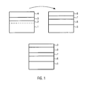
Figure 1 illustrates an example for the method for manufacturing a wafer comprising an intrinsic semiconductor layer according to the present invention. -
Figure 2 Illustrates an embedded DRAM device integrated with back-biased SOl transistors of a logic part manufactured on the basis on the wafer illustrated inFigure 1 . - A particular example for manufacturing a wafer in accordance with the present invention will now be described with reference to
Figure 1 . In a donor substrate 1 a nucleation layer 2 is formed by the implantation of ions. The implantation of ions results in a weakened zone at the main concentration of the implanted ions. The implantation energy may be in a range of some 5 keV to 20 keV and the implantation dose may be chosen to be in the range of 5 x 10¹⁶ to 1017 ions/cm2, for example. Asilicon layer 3 is formed on the donor substrate 1. Subsequently, anoxide layer 4 is formed atop of thesilicon layer 3. Anothersubstrate 5, for example, asilicon substrate 5 is provided. A dopedlayer 6, for example, a silicon layer doped with phosphorus dopants of a concentration of 1019 cm-3 , is formed on thesilicon substrate 5. Asilicon layer 7 is formed on the dopedlayer 6. For example,silicon layer 7 can be grown by epitaxy and some dopant can be added during the epitaxial growth. Then, another oxide layer 8 is formed atop. - The structure comprising the donor substrate 1 and the
silicon substrate 5 are then bonded to each other at the free surfaces of theoxide layers 4 and 8 as it is indicated by the arrow inFigure 1 . Next, stresses, for example, thermal and/or mechanical stresses are applied to the bonded structure in order to detach the donor substrate 1 and the nucleation layer 2. For this, the Smart Cut© process may be employed, i.e. a heat treatment is carried out at a temperature of about 500 °C to 600 °C, for a time period of about 30 minutes up to about 3 hours, for example. Alternatively, a laser lift-off technique that is also known in the art may be applied in order to detach the donor substrate 1. - After detachment and a surface treatment like grinding and/or chemical-mechanical polishing the wafer results that is illustrated in the lower sketch of
Figure 1 . On thesilicon substrate 5 it is arranged the dopedlayer 6. On the dopedlayer 6 it is arranged the first (intrinsic)silicon layer 7. On thesilicon layer 7 it is arranged a buriedoxide layer 9 resulting from the bondedoxide layers 4 and 8. On the buriedoxide layer 9 it is arranged thesecond silicon layer 3. Exemplary thicknesses of the individual layers of the wafer are as follows. The dopedlayer 6 may have a thickness of some µm, for example, 2 to 5 µm. The (intrinsic)silicon layer 7 may have a thickness of some 50 nm. The buriedoxide layer 9 may have a thickness of 5 to 25 nm and thetop silicon layer 3 may have a thickness of 5 to 20 nm. - In
Figure 2 an embedded DRAM device in a DRAM part A integrated with SOl transistors of a logic part B for addressing the DRAMs manufactured by means of the wafer shown inFigure 1 is illustrated. On the left-hand-side the DRAM part A is illustrated and on the right-hand side ofFigure 2 the logic part B is illustrated. In the DRAM part A a capacitordeep trench 10 extending to the dopedlayer 6 that functions as a capacitor back plate is illustrated. Acontrol FET 11 is formed in the DRAM part A with a channel region formed in theupper silicon layer 3. Thecontrol FET 11 may be realized as a fully depleted or partially depleted device. The thickness of theupper silicon layer 3 is chosen accordingly. - The DRAM part A and the logic part B are separated from each other by a
shallow trench isolation 12.Transistors 13 formed in the logic part B are also separated from each other byshallow trench isolation 12. Regions of thesilicon layer 7 can be easily converted into doped regions in order to form back-biasing regions for thetransistors 13. For example, a region of thesilicon layer 7 below theleft transistor 13 in the logic part B may be n doped with a concentration of some 1018 cm-3 whereas a region of thesilicon layer 7 below theright transistor 13 in the logic part B may be p doped with a concentration of some 1018 cm-3 depending on the Vt shift we want to induce in the transistor channels formed in theupper silicon layer 3.Figure 2 , moreover, showscontacts 14 for back-biasing. N back-biasing regions in the logic part B are connected with each other through the n+ doped dopedlayer 6. In order to ensure sufficient electrical resistivity between two back-biasing contacts it might be considered necessary to keep some part of theintrinsic silicon layer 7 undoped or p doped. Thus, theintrinsic silicon layer 7 might be provided with a thickness of some 100 to 300 nm. - It should be noted that the
shallow trench isolators 12 might be provided extending partly into the dopedlayer 6. They might also be provided extending through the dopedlayer 6 and into thesubstrate 5 thereby cutting the n+ dopedlayer 6. Different embedded DRAM blocks can be separated by suchshallow trench isolators 12 reaching into thesubstrate 5. - All previously discussed embodiments are not intended as limitations but serve as examples illustrating features and advantages of the invention. It is to be understood that some or all of the above described features can also be combined in different ways.
Claims (17)
- Method for the manufacture of a wafer, comprising the steps of
providing a doped layer on a semiconductor substrate;
providing a first semiconductor layer on the doped layer;
providing a buried oxide layer on the first semiconductor layer; and
providing a second semiconductor layer on the buried oxide layer. - The method according to claim 1, wherein the doped layer and the first semiconductor layer are grown on the semiconductor substrate.
- The method according to claim 1 or 2, wherein the wafer is obtained by bonding the first and the second semiconductor layers by the buried oxide layer and detaching the donator substrate.
- The method according to one of the preceding claims, wherein the buried oxide is formed on the first semiconductor layer or on the donator substrate.
- The method according to one of the preceding claims, wherein the second semiconductor layer is grown on a donor substrate.
- The method according to one of the preceding claims, wherein
the doped layer is an epitaxial doped layer grown on the semiconductor substrate;
and/or the first semiconductor layer is an epitaxial layer grown on the doped layer.
and/or wherein forming the second semiconductor layer on the buried oxide layer comprises
growing the second semiconductor layer on a donator substrate to obtain a donor wafer;
and/or forming a first oxide layer on the second semiconductor layer grown on the donor substrate; and/or
forming a second oxide layer on the epitaxial first semiconductor layer grown on the doped layer; and
bonding the donor wafer to the first semiconductor layer grown on the doped layer by the first and/or second intermediate buried layer, wherein the first and/or second oxide layer form the buried oxide layer, and
detaching the donor substrate. - The method according to one of the preceding claims, further comprising doping at least a region of the first semiconductor layer by n or p dopants.
- Method for the manufacture of a semiconductor device, comprising
providing a wafer obtained by a method according to one of the preceding claims;
forming an embedded DRAM device in a first region of the wafer; and
forming a back-biased transistor in a second region of the wafer that is different from the first region. - The method for the manufacture of a semiconductor device according to claim 8, wherein
forming the embedded DRAM device in the first region of the wafer comprises forming a capacitor trench extending from the second semiconductor layer at least partly into the doped layer; and
forming the back-biased transistor in the second region of the wafer that is separated from the first region by a shallow trench isolator comprises forming a back-biasing region in the first semiconductor layer. - The method for the manufacture of a semiconductor device according to claim 8, wherein forming the back-biasing region in the first semiconductor layer comprises doping at least a part of the first semiconductor layer of the already provided wafer with n or p dopants.
- Wafer comprising
a semiconductor substrate;
a doped layer formed on the semiconductor substrate;
a first semiconductor layer formed on the semiconductor substrate;
a buried oxide layer formed on the first semiconductor layer; and
a second semiconductor layer formed on the buried oxide layer. - The wafer according to claim 11, wherein the semiconductor substrate and/or the first semiconductor layer and/or the second semiconductor layer comprises or consists of silicon.
- The wafer according to claim 11 or 12, wherein the doped layer comprises n dopants, in particular, phosphorus dopants.
- The wafer according to one of the claims 11 to 13, wherein
the thickness of the first semiconductor layer is in the range of 10 to 300 nm, in particular, 50 to 150 nm; and/or
the thickness of the second semiconductor layer is in the range of 5 to 100 nm, in particular, 5 to 15 nm; and/or
the thickness of the buried oxide layer is in the range of 10 to 200 nm, in particular, 5 to 25 nm; and/or
the thickness of the doped layer is in the range of 1 to 10 µm. - Semiconductor device, comprising
a wafer according to one of the claims 11 to 14; and integrated on that wafer
an embedded DRAM device comprising a capacitor trench extending from the second semiconductor layer at least partly into the doped layer and a control FET having a channel region in the second semiconductor layer; and
a back-biased SOI transistor comprising a channel region in the second semiconductor layer and a doped back-biasing region in the first semiconductor layer and a contact for contacting the doped back-biasing region. - The semiconductor device according to claim 15, wherein the first semiconductor layer is doped in an upper region adjacent to the buried oxide layer and undoped in a lower region adjacent to the doped layer.
- The semiconductor device according to claim 15 or 16, comprising a number of back-biased SOl transistors separated from each other and from the embedded DRAM device by shallow trench isolators extending from the second semiconductor layer at least partly into the doped layer or through the doped layer into the semiconductor substrate.
Priority Applications (7)
| Application Number | Priority Date | Filing Date | Title |
|---|---|---|---|
| EP11290126.9A EP2498280B1 (en) | 2011-03-11 | 2011-03-11 | DRAM with trench capacitors and logic back-biased transistors integrated on an SOI substrate comprising an intrinsic semiconductor layer and manufacturing method thereof |
| SG2012006722A SG184629A1 (en) | 2011-03-11 | 2012-01-31 | Wafer with intrinsic semiconductor layer |
| TW101103153A TWI578495B (en) | 2011-03-11 | 2012-01-31 | Method of manufacturing semiconductor device and method of manufacturing wafer, and semiconductor device and wafer thereof |
| JP2012020132A JP5681976B2 (en) | 2011-03-11 | 2012-02-01 | Wafer with intrinsic semiconductor layer |
| CN201210058033.2A CN102709251B (en) | 2011-03-11 | 2012-03-07 | Wafer with intrinsic semiconductor layer |
| KR1020120024038A KR101395161B1 (en) | 2011-03-11 | 2012-03-08 | Wafer with intrinsic semiconductor layer |
| US13/416,739 US9177961B2 (en) | 2011-03-11 | 2012-03-09 | Wafer with intrinsic semiconductor layer |
Applications Claiming Priority (1)
| Application Number | Priority Date | Filing Date | Title |
|---|---|---|---|
| EP11290126.9A EP2498280B1 (en) | 2011-03-11 | 2011-03-11 | DRAM with trench capacitors and logic back-biased transistors integrated on an SOI substrate comprising an intrinsic semiconductor layer and manufacturing method thereof |
Publications (2)
| Publication Number | Publication Date |
|---|---|
| EP2498280A1 true EP2498280A1 (en) | 2012-09-12 |
| EP2498280B1 EP2498280B1 (en) | 2020-04-29 |
Family
ID=44278827
Family Applications (1)
| Application Number | Title | Priority Date | Filing Date |
|---|---|---|---|
| EP11290126.9A Active EP2498280B1 (en) | 2011-03-11 | 2011-03-11 | DRAM with trench capacitors and logic back-biased transistors integrated on an SOI substrate comprising an intrinsic semiconductor layer and manufacturing method thereof |
Country Status (7)
| Country | Link |
|---|---|
| US (1) | US9177961B2 (en) |
| EP (1) | EP2498280B1 (en) |
| JP (1) | JP5681976B2 (en) |
| KR (1) | KR101395161B1 (en) |
| CN (1) | CN102709251B (en) |
| SG (1) | SG184629A1 (en) |
| TW (1) | TWI578495B (en) |
Cited By (1)
| Publication number | Priority date | Publication date | Assignee | Title |
|---|---|---|---|---|
| WO2018035229A3 (en) * | 2016-08-16 | 2018-04-05 | Texas Instruments Incorporated | Dual deep trenches for high voltage isolation |
Families Citing this family (6)
| Publication number | Priority date | Publication date | Assignee | Title |
|---|---|---|---|---|
| CN103208737B (en) * | 2012-12-20 | 2016-01-20 | 上海显恒光电科技股份有限公司 | A kind of manufacture method and obtained ultraviolet light of ultraviolet light screen are shielded and apply |
| CN103413777B (en) * | 2013-08-22 | 2017-04-12 | 上海华虹宏力半导体制造有限公司 | Deep groove filling structure and manufacturing method thereof |
| US9666615B2 (en) | 2015-10-20 | 2017-05-30 | International Business Machines Corporation | Semiconductor on insulator substrate with back bias |
| JP6637831B2 (en) * | 2016-04-28 | 2020-01-29 | 株式会社ディスコ | Device manufacturing method and grinding device |
| FR3083000B1 (en) * | 2018-06-21 | 2024-11-29 | Soitec Silicon On Insulator | SUBSTRATE FOR FRONT-SIDE TYPE IMAGE SENSOR AND METHOD FOR MANUFACTURING SUCH SUBSTRATE |
| CN111415864A (en) * | 2020-03-18 | 2020-07-14 | 上海晶盟硅材料有限公司 | Super-heavy red phosphorus doped substrate epitaxy method |
Citations (4)
| Publication number | Priority date | Publication date | Assignee | Title |
|---|---|---|---|---|
| US20060202249A1 (en) * | 2005-03-08 | 2006-09-14 | International Business Machines Corporation | Simplified buried plate structure and process for semiconductor-on-insulator chip |
| US20090003105A1 (en) * | 2007-06-26 | 2009-01-01 | Kiyoo Itoh | Semiconductor device |
| US20090250738A1 (en) * | 2008-04-04 | 2009-10-08 | International Business Machines Corporation | Simultaneous buried strap and buried contact via formation for soi deep trench capacitor |
| US20100176453A1 (en) * | 2009-01-12 | 2010-07-15 | International Business Machines Corporation | Low cost fabrication of double box back gate silicon-on-insulator wafers with built-in shallow trench isolation in back gate layer |
Family Cites Families (11)
| Publication number | Priority date | Publication date | Assignee | Title |
|---|---|---|---|---|
| US5508219A (en) * | 1995-06-05 | 1996-04-16 | International Business Machines Corporation | SOI DRAM with field-shield isolation and body contact |
| US6441436B1 (en) * | 2000-11-29 | 2002-08-27 | United Microelectronics Corp. | SOI device and method of fabrication |
| US6657256B2 (en) * | 2001-05-22 | 2003-12-02 | General Semiconductor, Inc. | Trench DMOS transistor having a zener diode for protection from electro-static discharge |
| JP2003168789A (en) * | 2001-11-29 | 2003-06-13 | Shin Etsu Handotai Co Ltd | Manufacturing method of SOI wafer |
| JP3943932B2 (en) * | 2001-12-27 | 2007-07-11 | 株式会社東芝 | Manufacturing method of semiconductor device |
| JP2004207271A (en) * | 2002-12-20 | 2004-07-22 | Nec Electronics Corp | SOI substrate and semiconductor integrated circuit device |
| JP2005109186A (en) * | 2003-09-30 | 2005-04-21 | Sony Corp | Semiconductor substrate and manufacturing method thereof, semiconductor device and manufacturing method thereof |
| KR20050075638A (en) * | 2004-01-17 | 2005-07-21 | 삼성전자주식회사 | Method of fabricating trench capacitor using soi type wafer |
| US7172930B2 (en) | 2004-07-02 | 2007-02-06 | International Business Machines Corporation | Strained silicon-on-insulator by anodization of a buried p+ silicon germanium layer |
| JP5528667B2 (en) * | 2007-11-28 | 2014-06-25 | ルネサスエレクトロニクス株式会社 | Semiconductor device and method for controlling semiconductor device |
| TWI389322B (en) | 2008-09-16 | 2013-03-11 | Gintech Energy Corp | Method for manufacturing solar cell with differential doping |
-
2011
- 2011-03-11 EP EP11290126.9A patent/EP2498280B1/en active Active
-
2012
- 2012-01-31 TW TW101103153A patent/TWI578495B/en active
- 2012-01-31 SG SG2012006722A patent/SG184629A1/en unknown
- 2012-02-01 JP JP2012020132A patent/JP5681976B2/en active Active
- 2012-03-07 CN CN201210058033.2A patent/CN102709251B/en active Active
- 2012-03-08 KR KR1020120024038A patent/KR101395161B1/en active Active
- 2012-03-09 US US13/416,739 patent/US9177961B2/en active Active
Patent Citations (4)
| Publication number | Priority date | Publication date | Assignee | Title |
|---|---|---|---|---|
| US20060202249A1 (en) * | 2005-03-08 | 2006-09-14 | International Business Machines Corporation | Simplified buried plate structure and process for semiconductor-on-insulator chip |
| US20090003105A1 (en) * | 2007-06-26 | 2009-01-01 | Kiyoo Itoh | Semiconductor device |
| US20090250738A1 (en) * | 2008-04-04 | 2009-10-08 | International Business Machines Corporation | Simultaneous buried strap and buried contact via formation for soi deep trench capacitor |
| US20100176453A1 (en) * | 2009-01-12 | 2010-07-15 | International Business Machines Corporation | Low cost fabrication of double box back gate silicon-on-insulator wafers with built-in shallow trench isolation in back gate layer |
Non-Patent Citations (1)
| Title |
|---|
| YANG I Y ET AL: "SILICON-ON-INSULATOR-WITH-ACTIVE-SUBSTRATE (SOIAS) TECHNOLOGY", 1996 IEEE INTERNATIONAL SOI CONFERENCE PROCEEDINGS. SANIBEL ISLAND, FL., SEPT. 30 - OCT. 3, 1996; [PROCEEDINGS OF THE ANNUAL SOS/SOI TECHNOLOGY CONFERENCE. (FROM 1991 PROCEEDINGS OF THE INTERNATIONAL SOI CONFERENCE.) SILICON-ON-INSULATOR TECHNOLOGY A, 30 September 1996 (1996-09-30), pages 106/107, XP000736867, ISBN: 978-0-7803-3316-1 * |
Cited By (3)
| Publication number | Priority date | Publication date | Assignee | Title |
|---|---|---|---|---|
| WO2018035229A3 (en) * | 2016-08-16 | 2018-04-05 | Texas Instruments Incorporated | Dual deep trenches for high voltage isolation |
| EP3501040A4 (en) * | 2016-08-16 | 2019-06-26 | Texas Instruments Incorporated | DOUBLE DEEP TRENCHES FOR HIGH VOLTAGE INSULATION |
| US10580775B2 (en) | 2016-08-16 | 2020-03-03 | Texas Instruments Incorporated | Dual deep trenches for high voltage isolation |
Also Published As
| Publication number | Publication date |
|---|---|
| EP2498280B1 (en) | 2020-04-29 |
| SG184629A1 (en) | 2012-10-30 |
| US9177961B2 (en) | 2015-11-03 |
| KR101395161B1 (en) | 2014-05-27 |
| JP2012191176A (en) | 2012-10-04 |
| US20120228689A1 (en) | 2012-09-13 |
| TW201238034A (en) | 2012-09-16 |
| CN102709251A (en) | 2012-10-03 |
| KR20120104101A (en) | 2012-09-20 |
| TWI578495B (en) | 2017-04-11 |
| CN102709251B (en) | 2015-01-28 |
| JP5681976B2 (en) | 2015-03-11 |
Similar Documents
| Publication | Publication Date | Title |
|---|---|---|
| US7422956B2 (en) | Semiconductor device and method of making semiconductor device comprising multiple stacked hybrid orientation layers | |
| US9177961B2 (en) | Wafer with intrinsic semiconductor layer | |
| US20050093077A1 (en) | CMOS on hybrid substrate with different crystal orientations using silicon-to-silicon direct wafer bonding | |
| US7977167B2 (en) | Method of producing a field effect transistor arrangement | |
| US20080087959A1 (en) | Manufacturing method of semiconductor-on-insulator region structures | |
| US7235433B2 (en) | Silicon-on-insulator semiconductor device with silicon layers having different crystal orientations and method of forming the silicon-on-insulator semiconductor device | |
| US20060202249A1 (en) | Simplified buried plate structure and process for semiconductor-on-insulator chip | |
| US8058158B2 (en) | Hybrid semiconductor substrate including semiconductor-on-insulator region and method of making the same | |
| JP3664704B2 (en) | Semiconductor device | |
| US6642536B1 (en) | Hybrid silicon on insulator/bulk strained silicon technology | |
| US12347673B2 (en) | Method for forming a semiconductor structure having a porous semiconductor layer in RF devices | |
| US20210111249A1 (en) | Semiconductor Structure Having Porous Semiconductor Segment for RF Devices and Bulk Semiconductor Region for Non-RF Devices | |
| CN118737947A (en) | Semiconductor wafer and manufacturing method thereof, transistor structure and manufacturing method thereof | |
| TWI875728B (en) | Semiconductor structure for digital and radiofrequency applications | |
| JP2005064194A (en) | Semiconductor substrate having SOI structure, manufacturing method thereof, and semiconductor device | |
| CN115172257A (en) | Substrate structure on silicon nitride and preparation method thereof |
Legal Events
| Date | Code | Title | Description |
|---|---|---|---|
| PUAI | Public reference made under article 153(3) epc to a published international application that has entered the european phase |
Free format text: ORIGINAL CODE: 0009012 |
|
| AK | Designated contracting states |
Kind code of ref document: A1 Designated state(s): AL AT BE BG CH CY CZ DE DK EE ES FI FR GB GR HR HU IE IS IT LI LT LU LV MC MK MT NL NO PL PT RO RS SE SI SK SM TR |
|
| AX | Request for extension of the european patent |
Extension state: BA ME |
|
| 17P | Request for examination filed |
Effective date: 20121011 |
|
| 17Q | First examination report despatched |
Effective date: 20130219 |
|
| STAA | Information on the status of an ep patent application or granted ep patent |
Free format text: STATUS: EXAMINATION IS IN PROGRESS |
|
| REG | Reference to a national code |
Ref country code: DE Ref legal event code: R079 Ref document number: 602011066499 Country of ref document: DE Free format text: PREVIOUS MAIN CLASS: H01L0021334000 Ipc: H01L0021840000 |
|
| RIC1 | Information provided on ipc code assigned before grant |
Ipc: H01L 21/84 20060101AFI20190930BHEP Ipc: H01L 29/66 20060101ALI20190930BHEP Ipc: H01L 21/762 20060101ALI20190930BHEP Ipc: H01L 27/108 20060101ALI20190930BHEP Ipc: H01L 27/12 20060101ALI20190930BHEP |
|
| GRAP | Despatch of communication of intention to grant a patent |
Free format text: ORIGINAL CODE: EPIDOSNIGR1 |
|
| STAA | Information on the status of an ep patent application or granted ep patent |
Free format text: STATUS: GRANT OF PATENT IS INTENDED |
|
| INTG | Intention to grant announced |
Effective date: 20191129 |
|
| GRAS | Grant fee paid |
Free format text: ORIGINAL CODE: EPIDOSNIGR3 |
|
| RIN1 | Information on inventor provided before grant (corrected) |
Inventor name: DAVAL, NICOLAS Inventor name: AULNETTE, CECILE Inventor name: NGUYEN, BICH-YEN |
|
| GRAA | (expected) grant |
Free format text: ORIGINAL CODE: 0009210 |
|
| STAA | Information on the status of an ep patent application or granted ep patent |
Free format text: STATUS: THE PATENT HAS BEEN GRANTED |
|
| RIN1 | Information on inventor provided before grant (corrected) |
Inventor name: DAVAL, NICOLAS Inventor name: NGUYEN, BICH-YEN Inventor name: AULNETTE, CECILE |
|
| AK | Designated contracting states |
Kind code of ref document: B1 Designated state(s): AL AT BE BG CH CY CZ DE DK EE ES FI FR GB GR HR HU IE IS IT LI LT LU LV MC MK MT NL NO PL PT RO RS SE SI SK SM TR |
|
| REG | Reference to a national code |
Ref country code: GB Ref legal event code: FG4D |
|
| REG | Reference to a national code |
Ref country code: CH Ref legal event code: EP |
|
| REG | Reference to a national code |
Ref country code: DE Ref legal event code: R096 Ref document number: 602011066499 Country of ref document: DE |
|
| REG | Reference to a national code |
Ref country code: AT Ref legal event code: REF Ref document number: 1264567 Country of ref document: AT Kind code of ref document: T Effective date: 20200515 |
|
| REG | Reference to a national code |
Ref country code: IE Ref legal event code: FG4D |
|
| REG | Reference to a national code |
Ref country code: NL Ref legal event code: MP Effective date: 20200429 |
|
| REG | Reference to a national code |
Ref country code: LT Ref legal event code: MG4D |
|
| PG25 | Lapsed in a contracting state [announced via postgrant information from national office to epo] |
Ref country code: LT Free format text: LAPSE BECAUSE OF FAILURE TO SUBMIT A TRANSLATION OF THE DESCRIPTION OR TO PAY THE FEE WITHIN THE PRESCRIBED TIME-LIMIT Effective date: 20200429 Ref country code: GR Free format text: LAPSE BECAUSE OF FAILURE TO SUBMIT A TRANSLATION OF THE DESCRIPTION OR TO PAY THE FEE WITHIN THE PRESCRIBED TIME-LIMIT Effective date: 20200730 Ref country code: IS Free format text: LAPSE BECAUSE OF FAILURE TO SUBMIT A TRANSLATION OF THE DESCRIPTION OR TO PAY THE FEE WITHIN THE PRESCRIBED TIME-LIMIT Effective date: 20200829 Ref country code: SE Free format text: LAPSE BECAUSE OF FAILURE TO SUBMIT A TRANSLATION OF THE DESCRIPTION OR TO PAY THE FEE WITHIN THE PRESCRIBED TIME-LIMIT Effective date: 20200429 Ref country code: PT Free format text: LAPSE BECAUSE OF FAILURE TO SUBMIT A TRANSLATION OF THE DESCRIPTION OR TO PAY THE FEE WITHIN THE PRESCRIBED TIME-LIMIT Effective date: 20200831 Ref country code: FI Free format text: LAPSE BECAUSE OF FAILURE TO SUBMIT A TRANSLATION OF THE DESCRIPTION OR TO PAY THE FEE WITHIN THE PRESCRIBED TIME-LIMIT Effective date: 20200429 Ref country code: NO Free format text: LAPSE BECAUSE OF FAILURE TO SUBMIT A TRANSLATION OF THE DESCRIPTION OR TO PAY THE FEE WITHIN THE PRESCRIBED TIME-LIMIT Effective date: 20200729 |
|
| REG | Reference to a national code |
Ref country code: AT Ref legal event code: MK05 Ref document number: 1264567 Country of ref document: AT Kind code of ref document: T Effective date: 20200429 |
|
| PG25 | Lapsed in a contracting state [announced via postgrant information from national office to epo] |
Ref country code: RS Free format text: LAPSE BECAUSE OF FAILURE TO SUBMIT A TRANSLATION OF THE DESCRIPTION OR TO PAY THE FEE WITHIN THE PRESCRIBED TIME-LIMIT Effective date: 20200429 Ref country code: LV Free format text: LAPSE BECAUSE OF FAILURE TO SUBMIT A TRANSLATION OF THE DESCRIPTION OR TO PAY THE FEE WITHIN THE PRESCRIBED TIME-LIMIT Effective date: 20200429 Ref country code: BG Free format text: LAPSE BECAUSE OF FAILURE TO SUBMIT A TRANSLATION OF THE DESCRIPTION OR TO PAY THE FEE WITHIN THE PRESCRIBED TIME-LIMIT Effective date: 20200729 Ref country code: HR Free format text: LAPSE BECAUSE OF FAILURE TO SUBMIT A TRANSLATION OF THE DESCRIPTION OR TO PAY THE FEE WITHIN THE PRESCRIBED TIME-LIMIT Effective date: 20200429 |
|
| PG25 | Lapsed in a contracting state [announced via postgrant information from national office to epo] |
Ref country code: AL Free format text: LAPSE BECAUSE OF FAILURE TO SUBMIT A TRANSLATION OF THE DESCRIPTION OR TO PAY THE FEE WITHIN THE PRESCRIBED TIME-LIMIT Effective date: 20200429 Ref country code: NL Free format text: LAPSE BECAUSE OF FAILURE TO SUBMIT A TRANSLATION OF THE DESCRIPTION OR TO PAY THE FEE WITHIN THE PRESCRIBED TIME-LIMIT Effective date: 20200429 |
|
| PG25 | Lapsed in a contracting state [announced via postgrant information from national office to epo] |
Ref country code: RO Free format text: LAPSE BECAUSE OF FAILURE TO SUBMIT A TRANSLATION OF THE DESCRIPTION OR TO PAY THE FEE WITHIN THE PRESCRIBED TIME-LIMIT Effective date: 20200429 Ref country code: CZ Free format text: LAPSE BECAUSE OF FAILURE TO SUBMIT A TRANSLATION OF THE DESCRIPTION OR TO PAY THE FEE WITHIN THE PRESCRIBED TIME-LIMIT Effective date: 20200429 Ref country code: EE Free format text: LAPSE BECAUSE OF FAILURE TO SUBMIT A TRANSLATION OF THE DESCRIPTION OR TO PAY THE FEE WITHIN THE PRESCRIBED TIME-LIMIT Effective date: 20200429 Ref country code: SM Free format text: LAPSE BECAUSE OF FAILURE TO SUBMIT A TRANSLATION OF THE DESCRIPTION OR TO PAY THE FEE WITHIN THE PRESCRIBED TIME-LIMIT Effective date: 20200429 Ref country code: DK Free format text: LAPSE BECAUSE OF FAILURE TO SUBMIT A TRANSLATION OF THE DESCRIPTION OR TO PAY THE FEE WITHIN THE PRESCRIBED TIME-LIMIT Effective date: 20200429 Ref country code: AT Free format text: LAPSE BECAUSE OF FAILURE TO SUBMIT A TRANSLATION OF THE DESCRIPTION OR TO PAY THE FEE WITHIN THE PRESCRIBED TIME-LIMIT Effective date: 20200429 Ref country code: ES Free format text: LAPSE BECAUSE OF FAILURE TO SUBMIT A TRANSLATION OF THE DESCRIPTION OR TO PAY THE FEE WITHIN THE PRESCRIBED TIME-LIMIT Effective date: 20200429 |
|
| REG | Reference to a national code |
Ref country code: DE Ref legal event code: R097 Ref document number: 602011066499 Country of ref document: DE |
|
| PG25 | Lapsed in a contracting state [announced via postgrant information from national office to epo] |
Ref country code: SK Free format text: LAPSE BECAUSE OF FAILURE TO SUBMIT A TRANSLATION OF THE DESCRIPTION OR TO PAY THE FEE WITHIN THE PRESCRIBED TIME-LIMIT Effective date: 20200429 Ref country code: PL Free format text: LAPSE BECAUSE OF FAILURE TO SUBMIT A TRANSLATION OF THE DESCRIPTION OR TO PAY THE FEE WITHIN THE PRESCRIBED TIME-LIMIT Effective date: 20200429 |
|
| PLBE | No opposition filed within time limit |
Free format text: ORIGINAL CODE: 0009261 |
|
| STAA | Information on the status of an ep patent application or granted ep patent |
Free format text: STATUS: NO OPPOSITION FILED WITHIN TIME LIMIT |
|
| 26N | No opposition filed |
Effective date: 20210201 |
|
| PG25 | Lapsed in a contracting state [announced via postgrant information from national office to epo] |
Ref country code: SI Free format text: LAPSE BECAUSE OF FAILURE TO SUBMIT A TRANSLATION OF THE DESCRIPTION OR TO PAY THE FEE WITHIN THE PRESCRIBED TIME-LIMIT Effective date: 20200429 |
|
| PG25 | Lapsed in a contracting state [announced via postgrant information from national office to epo] |
Ref country code: MC Free format text: LAPSE BECAUSE OF FAILURE TO SUBMIT A TRANSLATION OF THE DESCRIPTION OR TO PAY THE FEE WITHIN THE PRESCRIBED TIME-LIMIT Effective date: 20200429 |
|
| REG | Reference to a national code |
Ref country code: CH Ref legal event code: PL |
|
| GBPC | Gb: european patent ceased through non-payment of renewal fee |
Effective date: 20210311 |
|
| PG25 | Lapsed in a contracting state [announced via postgrant information from national office to epo] |
Ref country code: IE Free format text: LAPSE BECAUSE OF NON-PAYMENT OF DUE FEES Effective date: 20210311 Ref country code: GB Free format text: LAPSE BECAUSE OF NON-PAYMENT OF DUE FEES Effective date: 20210311 Ref country code: CH Free format text: LAPSE BECAUSE OF NON-PAYMENT OF DUE FEES Effective date: 20210331 Ref country code: LI Free format text: LAPSE BECAUSE OF NON-PAYMENT OF DUE FEES Effective date: 20210331 Ref country code: LU Free format text: LAPSE BECAUSE OF NON-PAYMENT OF DUE FEES Effective date: 20210311 |
|
| PG25 | Lapsed in a contracting state [announced via postgrant information from national office to epo] |
Ref country code: HU Free format text: LAPSE BECAUSE OF FAILURE TO SUBMIT A TRANSLATION OF THE DESCRIPTION OR TO PAY THE FEE WITHIN THE PRESCRIBED TIME-LIMIT; INVALID AB INITIO Effective date: 20110311 Ref country code: CY Free format text: LAPSE BECAUSE OF FAILURE TO SUBMIT A TRANSLATION OF THE DESCRIPTION OR TO PAY THE FEE WITHIN THE PRESCRIBED TIME-LIMIT Effective date: 20200429 |
|
| PG25 | Lapsed in a contracting state [announced via postgrant information from national office to epo] |
Ref country code: MK Free format text: LAPSE BECAUSE OF FAILURE TO SUBMIT A TRANSLATION OF THE DESCRIPTION OR TO PAY THE FEE WITHIN THE PRESCRIBED TIME-LIMIT Effective date: 20200429 |
|
| PG25 | Lapsed in a contracting state [announced via postgrant information from national office to epo] |
Ref country code: TR Free format text: LAPSE BECAUSE OF FAILURE TO SUBMIT A TRANSLATION OF THE DESCRIPTION OR TO PAY THE FEE WITHIN THE PRESCRIBED TIME-LIMIT Effective date: 20200429 |
|
| PG25 | Lapsed in a contracting state [announced via postgrant information from national office to epo] |
Ref country code: MT Free format text: LAPSE BECAUSE OF FAILURE TO SUBMIT A TRANSLATION OF THE DESCRIPTION OR TO PAY THE FEE WITHIN THE PRESCRIBED TIME-LIMIT Effective date: 20200429 |
|
| REG | Reference to a national code |
Ref country code: DE Ref legal event code: R079 Ref document number: 602011066499 Country of ref document: DE Free format text: PREVIOUS MAIN CLASS: H01L0021840000 Ipc: H10D0086010000 |
|
| PGFP | Annual fee paid to national office [announced via postgrant information from national office to epo] |
Ref country code: DE Payment date: 20260204 Year of fee payment: 16 |
|
| PGFP | Annual fee paid to national office [announced via postgrant information from national office to epo] |
Ref country code: BE Payment date: 20260216 Year of fee payment: 16 Ref country code: IT Payment date: 20260220 Year of fee payment: 16 |
|
| PGFP | Annual fee paid to national office [announced via postgrant information from national office to epo] |
Ref country code: FR Payment date: 20260223 Year of fee payment: 16 |