EP2492933A2 - Grain Boundary-Insulated Semiconductor Ceramic, Semiconductor Ceramic Capacitor, and Method for Producing Semiconductor Ceramic Capacitor - Google Patents
Grain Boundary-Insulated Semiconductor Ceramic, Semiconductor Ceramic Capacitor, and Method for Producing Semiconductor Ceramic Capacitor Download PDFInfo
- Publication number
- EP2492933A2 EP2492933A2 EP12156385A EP12156385A EP2492933A2 EP 2492933 A2 EP2492933 A2 EP 2492933A2 EP 12156385 A EP12156385 A EP 12156385A EP 12156385 A EP12156385 A EP 12156385A EP 2492933 A2 EP2492933 A2 EP 2492933A2
- Authority
- EP
- European Patent Office
- Prior art keywords
- grain boundary
- semiconductor ceramic
- component
- insulating agent
- boundary insulating
- Prior art date
- Legal status (The legal status is an assumption and is not a legal conclusion. Google has not performed a legal analysis and makes no representation as to the accuracy of the status listed.)
- Granted
Links
Images

Classifications
-
- H—ELECTRICITY
- H01—ELECTRIC ELEMENTS
- H01G—CAPACITORS; CAPACITORS, RECTIFIERS, DETECTORS, SWITCHING DEVICES, LIGHT-SENSITIVE OR TEMPERATURE-SENSITIVE DEVICES OF THE ELECTROLYTIC TYPE
- H01G4/00—Fixed capacitors; Processes of their manufacture
- H01G4/002—Details
- H01G4/018—Dielectrics
- H01G4/06—Solid dielectrics
- H01G4/08—Inorganic dielectrics
- H01G4/12—Ceramic dielectrics
- H01G4/1209—Ceramic dielectrics characterised by the ceramic dielectric material
- H01G4/1218—Ceramic dielectrics characterised by the ceramic dielectric material based on titanium oxides or titanates
- H01G4/1227—Ceramic dielectrics characterised by the ceramic dielectric material based on titanium oxides or titanates based on alkaline earth titanates
-
- C—CHEMISTRY; METALLURGY
- C03—GLASS; MINERAL OR SLAG WOOL
- C03C—CHEMICAL COMPOSITION OF GLASSES, GLAZES OR VITREOUS ENAMELS; SURFACE TREATMENT OF GLASS; SURFACE TREATMENT OF FIBRES OR FILAMENTS MADE FROM GLASS, MINERALS OR SLAGS; JOINING GLASS TO GLASS OR OTHER MATERIALS
- C03C14/00—Glass compositions containing a non-glass component, e.g. compositions containing fibres, filaments, whiskers, platelets, or the like, dispersed in a glass matrix
- C03C14/004—Glass compositions containing a non-glass component, e.g. compositions containing fibres, filaments, whiskers, platelets, or the like, dispersed in a glass matrix the non-glass component being in the form of particles or flakes
-
- C—CHEMISTRY; METALLURGY
- C03—GLASS; MINERAL OR SLAG WOOL
- C03C—CHEMICAL COMPOSITION OF GLASSES, GLAZES OR VITREOUS ENAMELS; SURFACE TREATMENT OF GLASS; SURFACE TREATMENT OF FIBRES OR FILAMENTS MADE FROM GLASS, MINERALS OR SLAGS; JOINING GLASS TO GLASS OR OTHER MATERIALS
- C03C3/00—Glass compositions
- C03C3/04—Glass compositions containing silica
- C03C3/076—Glass compositions containing silica with 40% to 90% silica, by weight
- C03C3/083—Glass compositions containing silica with 40% to 90% silica, by weight containing aluminium oxide or an iron compound
- C03C3/085—Glass compositions containing silica with 40% to 90% silica, by weight containing aluminium oxide or an iron compound containing an oxide of a divalent metal
- C03C3/087—Glass compositions containing silica with 40% to 90% silica, by weight containing aluminium oxide or an iron compound containing an oxide of a divalent metal containing calcium oxide, e.g. common sheet or container glass
-
- C—CHEMISTRY; METALLURGY
- C04—CEMENTS; CONCRETE; ARTIFICIAL STONE; CERAMICS; REFRACTORIES
- C04B—LIME, MAGNESIA; SLAG; CEMENTS; COMPOSITIONS THEREOF, e.g. MORTARS, CONCRETE OR LIKE BUILDING MATERIALS; ARTIFICIAL STONE; CERAMICS; REFRACTORIES; TREATMENT OF NATURAL STONE
- C04B35/00—Shaped ceramic products characterised by their composition; Ceramics compositions; Processing powders of inorganic compounds preparatory to the manufacturing of ceramic products
- C04B35/01—Shaped ceramic products characterised by their composition; Ceramics compositions; Processing powders of inorganic compounds preparatory to the manufacturing of ceramic products based on oxide ceramics
- C04B35/46—Shaped ceramic products characterised by their composition; Ceramics compositions; Processing powders of inorganic compounds preparatory to the manufacturing of ceramic products based on oxide ceramics based on titanium oxides or titanates
- C04B35/462—Shaped ceramic products characterised by their composition; Ceramics compositions; Processing powders of inorganic compounds preparatory to the manufacturing of ceramic products based on oxide ceramics based on titanium oxides or titanates based on titanates
- C04B35/465—Shaped ceramic products characterised by their composition; Ceramics compositions; Processing powders of inorganic compounds preparatory to the manufacturing of ceramic products based on oxide ceramics based on titanium oxides or titanates based on titanates based on alkaline earth metal titanates
- C04B35/47—Shaped ceramic products characterised by their composition; Ceramics compositions; Processing powders of inorganic compounds preparatory to the manufacturing of ceramic products based on oxide ceramics based on titanium oxides or titanates based on titanates based on alkaline earth metal titanates based on strontium titanates
-
- H—ELECTRICITY
- H01—ELECTRIC ELEMENTS
- H01G—CAPACITORS; CAPACITORS, RECTIFIERS, DETECTORS, SWITCHING DEVICES, LIGHT-SENSITIVE OR TEMPERATURE-SENSITIVE DEVICES OF THE ELECTROLYTIC TYPE
- H01G4/00—Fixed capacitors; Processes of their manufacture
- H01G4/002—Details
- H01G4/018—Dielectrics
- H01G4/06—Solid dielectrics
- H01G4/08—Inorganic dielectrics
- H01G4/12—Ceramic dielectrics
- H01G4/1272—Semiconductive ceramic capacitors
- H01G4/1281—Semiconductive ceramic capacitors with grain boundary layer
-
- H—ELECTRICITY
- H01—ELECTRIC ELEMENTS
- H01G—CAPACITORS; CAPACITORS, RECTIFIERS, DETECTORS, SWITCHING DEVICES, LIGHT-SENSITIVE OR TEMPERATURE-SENSITIVE DEVICES OF THE ELECTROLYTIC TYPE
- H01G4/00—Fixed capacitors; Processes of their manufacture
- H01G4/002—Details
- H01G4/018—Dielectrics
- H01G4/06—Solid dielectrics
- H01G4/08—Inorganic dielectrics
- H01G4/12—Ceramic dielectrics
- H01G4/129—Ceramic dielectrics containing a glassy phase, e.g. glass ceramic
-
- C—CHEMISTRY; METALLURGY
- C03—GLASS; MINERAL OR SLAG WOOL
- C03C—CHEMICAL COMPOSITION OF GLASSES, GLAZES OR VITREOUS ENAMELS; SURFACE TREATMENT OF GLASS; SURFACE TREATMENT OF FIBRES OR FILAMENTS MADE FROM GLASS, MINERALS OR SLAGS; JOINING GLASS TO GLASS OR OTHER MATERIALS
- C03C2214/00—Nature of the non-vitreous component
- C03C2214/20—Glass-ceramics matrix
-
- C—CHEMISTRY; METALLURGY
- C04—CEMENTS; CONCRETE; ARTIFICIAL STONE; CERAMICS; REFRACTORIES
- C04B—LIME, MAGNESIA; SLAG; CEMENTS; COMPOSITIONS THEREOF, e.g. MORTARS, CONCRETE OR LIKE BUILDING MATERIALS; ARTIFICIAL STONE; CERAMICS; REFRACTORIES; TREATMENT OF NATURAL STONE
- C04B2235/00—Aspects relating to ceramic starting mixtures or sintered ceramic products
- C04B2235/02—Composition of constituents of the starting material or of secondary phases of the final product
- C04B2235/30—Constituents and secondary phases not being of a fibrous nature
- C04B2235/32—Metal oxides, mixed metal oxides, or oxide-forming salts thereof, e.g. carbonates, nitrates, (oxy)hydroxides, chlorides
- C04B2235/3205—Alkaline earth oxides or oxide forming salts thereof, e.g. beryllium oxide
- C04B2235/3208—Calcium oxide or oxide-forming salts thereof, e.g. lime
-
- C—CHEMISTRY; METALLURGY
- C04—CEMENTS; CONCRETE; ARTIFICIAL STONE; CERAMICS; REFRACTORIES
- C04B—LIME, MAGNESIA; SLAG; CEMENTS; COMPOSITIONS THEREOF, e.g. MORTARS, CONCRETE OR LIKE BUILDING MATERIALS; ARTIFICIAL STONE; CERAMICS; REFRACTORIES; TREATMENT OF NATURAL STONE
- C04B2235/00—Aspects relating to ceramic starting mixtures or sintered ceramic products
- C04B2235/02—Composition of constituents of the starting material or of secondary phases of the final product
- C04B2235/30—Constituents and secondary phases not being of a fibrous nature
- C04B2235/32—Metal oxides, mixed metal oxides, or oxide-forming salts thereof, e.g. carbonates, nitrates, (oxy)hydroxides, chlorides
- C04B2235/3224—Rare earth oxide or oxide forming salts thereof, e.g. scandium oxide
- C04B2235/3225—Yttrium oxide or oxide-forming salts thereof
-
- C—CHEMISTRY; METALLURGY
- C04—CEMENTS; CONCRETE; ARTIFICIAL STONE; CERAMICS; REFRACTORIES
- C04B—LIME, MAGNESIA; SLAG; CEMENTS; COMPOSITIONS THEREOF, e.g. MORTARS, CONCRETE OR LIKE BUILDING MATERIALS; ARTIFICIAL STONE; CERAMICS; REFRACTORIES; TREATMENT OF NATURAL STONE
- C04B2235/00—Aspects relating to ceramic starting mixtures or sintered ceramic products
- C04B2235/02—Composition of constituents of the starting material or of secondary phases of the final product
- C04B2235/30—Constituents and secondary phases not being of a fibrous nature
- C04B2235/32—Metal oxides, mixed metal oxides, or oxide-forming salts thereof, e.g. carbonates, nitrates, (oxy)hydroxides, chlorides
- C04B2235/3281—Copper oxides, cuprates or oxide-forming salts thereof, e.g. CuO or Cu2O
-
- C—CHEMISTRY; METALLURGY
- C04—CEMENTS; CONCRETE; ARTIFICIAL STONE; CERAMICS; REFRACTORIES
- C04B—LIME, MAGNESIA; SLAG; CEMENTS; COMPOSITIONS THEREOF, e.g. MORTARS, CONCRETE OR LIKE BUILDING MATERIALS; ARTIFICIAL STONE; CERAMICS; REFRACTORIES; TREATMENT OF NATURAL STONE
- C04B2235/00—Aspects relating to ceramic starting mixtures or sintered ceramic products
- C04B2235/02—Composition of constituents of the starting material or of secondary phases of the final product
- C04B2235/30—Constituents and secondary phases not being of a fibrous nature
- C04B2235/32—Metal oxides, mixed metal oxides, or oxide-forming salts thereof, e.g. carbonates, nitrates, (oxy)hydroxides, chlorides
- C04B2235/3298—Bismuth oxides, bismuthates or oxide forming salts thereof, e.g. zinc bismuthate
-
- C—CHEMISTRY; METALLURGY
- C04—CEMENTS; CONCRETE; ARTIFICIAL STONE; CERAMICS; REFRACTORIES
- C04B—LIME, MAGNESIA; SLAG; CEMENTS; COMPOSITIONS THEREOF, e.g. MORTARS, CONCRETE OR LIKE BUILDING MATERIALS; ARTIFICIAL STONE; CERAMICS; REFRACTORIES; TREATMENT OF NATURAL STONE
- C04B2235/00—Aspects relating to ceramic starting mixtures or sintered ceramic products
- C04B2235/02—Composition of constituents of the starting material or of secondary phases of the final product
- C04B2235/30—Constituents and secondary phases not being of a fibrous nature
- C04B2235/36—Glass starting materials for making ceramics, e.g. silica glass
-
- C—CHEMISTRY; METALLURGY
- C04—CEMENTS; CONCRETE; ARTIFICIAL STONE; CERAMICS; REFRACTORIES
- C04B—LIME, MAGNESIA; SLAG; CEMENTS; COMPOSITIONS THEREOF, e.g. MORTARS, CONCRETE OR LIKE BUILDING MATERIALS; ARTIFICIAL STONE; CERAMICS; REFRACTORIES; TREATMENT OF NATURAL STONE
- C04B2235/00—Aspects relating to ceramic starting mixtures or sintered ceramic products
- C04B2235/65—Aspects relating to heat treatments of ceramic bodies such as green ceramics or pre-sintered ceramics, e.g. burning, sintering or melting processes
- C04B2235/652—Reduction treatment
-
- C—CHEMISTRY; METALLURGY
- C04—CEMENTS; CONCRETE; ARTIFICIAL STONE; CERAMICS; REFRACTORIES
- C04B—LIME, MAGNESIA; SLAG; CEMENTS; COMPOSITIONS THEREOF, e.g. MORTARS, CONCRETE OR LIKE BUILDING MATERIALS; ARTIFICIAL STONE; CERAMICS; REFRACTORIES; TREATMENT OF NATURAL STONE
- C04B2235/00—Aspects relating to ceramic starting mixtures or sintered ceramic products
- C04B2235/65—Aspects relating to heat treatments of ceramic bodies such as green ceramics or pre-sintered ceramics, e.g. burning, sintering or melting processes
- C04B2235/658—Atmosphere during thermal treatment
- C04B2235/6582—Hydrogen containing atmosphere
-
- C—CHEMISTRY; METALLURGY
- C04—CEMENTS; CONCRETE; ARTIFICIAL STONE; CERAMICS; REFRACTORIES
- C04B—LIME, MAGNESIA; SLAG; CEMENTS; COMPOSITIONS THEREOF, e.g. MORTARS, CONCRETE OR LIKE BUILDING MATERIALS; ARTIFICIAL STONE; CERAMICS; REFRACTORIES; TREATMENT OF NATURAL STONE
- C04B2235/00—Aspects relating to ceramic starting mixtures or sintered ceramic products
- C04B2235/65—Aspects relating to heat treatments of ceramic bodies such as green ceramics or pre-sintered ceramics, e.g. burning, sintering or melting processes
- C04B2235/658—Atmosphere during thermal treatment
- C04B2235/6587—Influencing the atmosphere by vaporising a solid material, e.g. by using a burying of sacrificial powder
-
- C—CHEMISTRY; METALLURGY
- C04—CEMENTS; CONCRETE; ARTIFICIAL STONE; CERAMICS; REFRACTORIES
- C04B—LIME, MAGNESIA; SLAG; CEMENTS; COMPOSITIONS THEREOF, e.g. MORTARS, CONCRETE OR LIKE BUILDING MATERIALS; ARTIFICIAL STONE; CERAMICS; REFRACTORIES; TREATMENT OF NATURAL STONE
- C04B2235/00—Aspects relating to ceramic starting mixtures or sintered ceramic products
- C04B2235/70—Aspects relating to sintered or melt-casted ceramic products
- C04B2235/72—Products characterised by the absence or the low content of specific components, e.g. alkali metal free alumina ceramics
-
- C—CHEMISTRY; METALLURGY
- C04—CEMENTS; CONCRETE; ARTIFICIAL STONE; CERAMICS; REFRACTORIES
- C04B—LIME, MAGNESIA; SLAG; CEMENTS; COMPOSITIONS THEREOF, e.g. MORTARS, CONCRETE OR LIKE BUILDING MATERIALS; ARTIFICIAL STONE; CERAMICS; REFRACTORIES; TREATMENT OF NATURAL STONE
- C04B2235/00—Aspects relating to ceramic starting mixtures or sintered ceramic products
- C04B2235/70—Aspects relating to sintered or melt-casted ceramic products
- C04B2235/74—Physical characteristics
- C04B2235/76—Crystal structural characteristics, e.g. symmetry
- C04B2235/768—Perovskite structure ABO3
-
- C—CHEMISTRY; METALLURGY
- C04—CEMENTS; CONCRETE; ARTIFICIAL STONE; CERAMICS; REFRACTORIES
- C04B—LIME, MAGNESIA; SLAG; CEMENTS; COMPOSITIONS THEREOF, e.g. MORTARS, CONCRETE OR LIKE BUILDING MATERIALS; ARTIFICIAL STONE; CERAMICS; REFRACTORIES; TREATMENT OF NATURAL STONE
- C04B2235/00—Aspects relating to ceramic starting mixtures or sintered ceramic products
- C04B2235/70—Aspects relating to sintered or melt-casted ceramic products
- C04B2235/80—Phases present in the sintered or melt-cast ceramic products other than the main phase
- C04B2235/85—Intergranular or grain boundary phases
Definitions
- the invention relates to a grain boundary-insulated semiconductor ceramic, a semiconductor ceramic capacitor, and a method for producing a semiconductor ceramic capacitor. More specifically, the present invention relates to a grain boundary-insulated semiconductor ceramic containing SrTiO 3 as a main component and a diffusing agent that contains a grain boundary insulating agent and a glass component, a semiconductor ceramic capacitor including the grain boundary-insulated semiconductor ceramic, and a method for producing the semiconductor ceramic capacitor.
- Grain boundary-insulated semiconductor ceramic capacitors are capacitors in which the apparent dielectric constant is increased by forming semiconductor crystal grains and insulating crystal grain boundaries, and are widely known as capacitors having small sizes and large capacitances.
- Japanese Unexamined Patent Application Publication No. 3-285870 discloses a grain boundary-insulated semiconductor porcelain composition in which a crystal grain boundary of semiconductor porcelain represented by a general formula (Sr 1-x-z Ba x Ca z M y ) + TiO 3 + mN + nZ (where M represents at least one element selected from Nb, Ta, W, and rare-earth elements, N represents at least one element selected from Mn, Al, etc., and Z represents at least one of Pb and B) wherein x, y, z, l, m, and n are each within a predetermined range is insulated by a compound containing at least one of Cu, Bi, Pb, B, and Si.
- a crystal grain boundary of semiconductor porcelain represented by a general formula (Sr 1-x-z Ba x Ca z M y ) + TiO 3 + mN + nZ (where M represents at least one element selected from Nb, Ta, W, and rare-earth elements, N represents at least one element selected
- JP 3-285870 in semiconductor porcelain containing SrTiO 3 as a main component, a Bi 2 O 3 -Pb 3 O 4 -B 2 O 3 -CuO-SiO 2 -based material is used as a grain boundary insulating agent that insulates grain boundaries, and this material is diffused during heat treatment to form a desired grain boundary insulating layer.
- a semiconductor ceramic capacitor having a large product of the apparent dielectric constant and the breakdown voltage is obtained.
- Japanese Unexamined Patent Application Publication No. 2-111006 discloses a method for producing a grain boundary-insulated semiconductor porcelain capacitor, the method including steps of preparing semiconductor porcelain; mixing the semiconductor porcelain with a diffusing agent prepared by adding a glass powder to a grain boundary insulating agent that insulates grain boundaries of the semiconductor porcelain in an amount of 1% by weight to 100% by weight relative to the grain boundary insulating agent, and heat-treating the resulting mixture while stirring to insulate the grain boundaries of the semiconductor porcelain; and forming electrodes by plating on both main surfaces of the semiconductor porcelain whose grain boundaries have been insulated.
- JP 2-111006 a diffusing agent containing a Bi 2 O 3 -PbO-CuO-based grain boundary insulating agent and a Bi 2 O 3 -PbO-CuO-B 2 O 3 -based glass powder is mixed and stirred with SrTiO 3 -based semiconductor porcelain to prepare semiconductor porcelain.
- variations in electrostatic capacity are reduced.
- JP 3-285870 a Bi 2 O 3 -Pb 3 O 4 -B 2 O 3 -CuO-SiO 2 -based material, which contains Pb, is used as a grain boundary insulating agent.
- the content of Pb 3 O 4 is a little less than 1/2.
- the grain boundary insulating agent does not sufficiently thermally diffuse into the inside of the capacitor, which may result in a decrease in electrical properties.
- JP 2-111006 Pb is used in both the grain boundary insulating agent and the glass powder, and thus the same problem as that in JP 3-285870 occurs.
- boron (B) is contained in the glass component. In the case where B is incorporated in the glass component, although the effect of increasing the diffusing power can be obtained to a certain degree, the insulation resistance and the breakdown voltage tend to decrease, which may result in a decrease in electrical properties.
- a grain boundary-insulated semiconductor ceramic includes a SrTiO 3 -based compound as a main component, and a diffusing agent containing a grain boundary insulating agent and a glass component, wherein the grain boundary insulating agent is composed of a non-lead material free of lead, the glass component mainly contains a SiO 2 -X 2 O-MO-TiO 2 -based glass material that does not contain boron or lead (where X represents an alkali metal, and M represents at least one selected from barium, strontium, and calcium), and the content of the glass component is 3 to 15 parts by weight relative to 100 parts by weight of the grain boundary insulating agent.
- the grain boundary insulating agent preferably contains at least bismuth and copper.
- the content of the grain boundary insulating agent is preferably 0.8 to 1.5 parts by weight relative to 100 parts by weight of the main component
- the alkali metal X in the glass component is preferably lithium.
- a semiconductor ceramic capacitor according to a preferred embodiment of the present invention includes a component base composed of any of the above grain boundary-insulated semiconductor ceramics.
- the component base preferably has a tubular shape, and an electrode is preferably provided on each of an inner peripheral surface and an outer peripheral surface of the component base.
- a method for producing a semiconductor ceramic capacitor includes the steps of preparing a sintered body by mixing a plurality of ceramic raw materials including at least a strontium compound and a titanium compound and firing the resulting mixture in a reducing atmosphere, weighing a grain boundary insulating agent composed of a non-lead material free of lead and a glass component composed of a SiO 2 -X 2 O-MO-TiO 2 -based glass material that does not contain boron or lead (where X represents an alkali metal, and M represents at least one selected from barium, strontium, and calcium), and preparing a component base by performing heat treatment in an air atmosphere while mixing and stirring the sintered body with the grain boundary insulating agent and the glass component.
- the sintered body is preferably prepared so as to have a tubular shape, and the method preferably further includes a step of forming an electrode on each of an inner peripheral surface and an outer peripheral surface of the component base by a plating process.
- the grain boundary insulating agent and the glass component are preferably weighed so that the amount of the glass component is 3 to 15 parts by weight relative to 100 parts by weight of the grain boundary insulating agent.
- the grain boundary insulating agent is composed of a non-Pb material free of Pb, such as a Bi-Cu-based material
- the glass component contains, as a main component, a SiO 2 -X 2 O-MO-TiO 2 -based glass material that does not contain B or Pb (where X represents an alkali metal such as Li, and M represents at least one selected from Ba, Sr, and Ca), and the content of the glass component is 3 to 15 parts by weight relative to 100 parts by weight of the grain boundary insulating agent. Accordingly, even though Pb is not contained, it is possible to obtain a grain boundary-insulated semiconductor ceramic having electrical properties equal to or better than those in the case where a Pb-based diffusing agent is used without causing a decrease in the insulation resistance or the breakdown voltage.
- a component base is composed of the above-described grain boundary-insulated semiconductor ceramic. Accordingly, even in the case where a non-Pb material is used as a semiconductor ceramic, a semiconductor ceramic capacitor having good electrical properties can be obtained.
- the component base is formed so as to have a tubular shape, and an electrode is formed on each of the inner peripheral surface and the outer peripheral surface of the component base, and thus the diffusing agent is uniformly or substantially uniformly distributed over the entire component base. Therefore, even in the case where the component base has a large wall thickness, it is possible to obtain a semiconductor ceramic capacitor that has good electrical properties such as the electrostatic capacity, the insulation resistance, and the breakdown voltage and that is excellent in terms of practical use.
- the method for producing a semiconductor ceramic capacitor includes the steps of preparing a sintered body by mixing a plurality of ceramic raw materials including at least a strontium compound and a titanium compound and firing the resulting mixture in a reducing atmosphere, weighing a grain boundary insulating agent composed of a non-lead material free of lead and a glass component composed of a SiO 2 -X 2 O-MO-TiO 2 -based glass material that does not contain boron or lead (where X represents an alkali metal, and M represents at least one selected from barium, strontium, and calcium), and preparing a component base by performing heat treatment in an air atmosphere while mixing and stirring the sintered body with the grain boundary insulating agent and the glass component.
- the diffusing agent containing the grain boundary insulating agent and the glass component has a diffusing power substantially the same as that of a lead-based diffusing agent. Therefore, even when a sintered body has a tubular shape having a large wall thickness, the diffusing agent can be uniformly or substantially uniformly distributed in the component base. Thus, grain boundaries can be uniformly oxidized, and a desired grain boundary insulating layer can be formed.
- the semiconductor ceramic capacitor thus obtained has good electrical properties such as the electrostatic capacity, the insulation resistance, and the breakdown voltage, and is excellent in terms of practical use.
- the inventor of the present invention has conducted intensive studies in order to achieve the above object. As a result, it was found that, by using a non-Pb material free of Pb, such as a Bi-Cu-based material, as a grain boundary insulating agent and using a SiO 2 -X 2 O-MO-TiO 2 -based glass material that does not contain B or Pb (where X represents an alkali metal and M represents at least one selected from Ba, Sr, and Ca) as a glass component, a grain boundary-insulated semiconductor ceramic having good electrical properties can be obtained without decreasing the insulation resistance or the breakdown voltage, even though a diffusing agent is composed of a non-Pb material.
- a non-Pb material free of Pb such as a Bi-Cu-based material
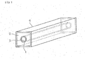
- Fig. 1 is a perspective view that schematically illustrates an embodiment of a semiconductor ceramic capacitor obtained using a grain boundary-insulated semiconductor ceramic of the present invention.
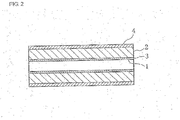
- Fig. 2 is a longitudinal cross-sectional view of Fig. 1 .
- the semiconductor ceramic capacitor includes a component base 2 which has a shape of a substantially rectangular tube and in which a through-hole 1 is formed.
- An inner peripheral electrode 3 is formed on the inner peripheral surface of the component base 2, and an outer peripheral electrode 4 is formed on the outer peripheral surface of the component base 2.
- this semiconductor ceramic capacitor is sandwiched and fixed between a pair of inductance elements such as ferrite beads, and widely used as a noise filter.
- the component base 2 is specifically composed of a grain boundary-insulated semiconductor ceramic.
- This grain boundary-insulated semiconductor ceramic is made up of an aggregate containing semiconductor crystal grains and a grain boundary insulating layer formed around the crystal grains.
- the crystal grains form an electrostatic capacity with the grain boundary insulating layer therebetween,
- the grain boundary-insulated semiconductor ceramic contains a SrTiO 3 -based material as a main component and a diffusing agent as an accessory component.
- semiconductor crystal grains are formed by a firing treatment in a reducing atmosphere, and a metal oxide is thermally diffused from the surfaces of the crystal grains by heat treatment performed after the firing treatment so that crystal grain boundaries are oxidized and insulated. Thus, a grain boundary insulating layer is formed.
- the diffusing agent contains a grain boundary insulating agent that contributes to insulate crystal grain boundaries and a glass component that functions as a thermal diffusion promoting agent.
- a non-Pb material free of Pb is used as the grain boundary insulating agent. Since Pb causes environmental pollution, Pb is eliminated from this grain boundary insulating agent in order to reduce the environmental burden.
- the grain boundary insulating agent is not particularly limited as long as the grain boundary insulating agent is composed of a non-Pb material and forms a desired grain boundary insulating layer by thermal diffusion. However, from the standpoint of obtaining electrical properties equal to or better than those obtained in the case where a Pb-based material is used, a metal oxide containing at least Bi and Cu is preferably used as the grain boundary insulating agent.
- the glass component contains, as a main component, a SiO 2 -X 2 O-MO-TiO 2 -based glass material that does not contain B or Pb.
- X represents an alkali metal, and typical examples of the alkali metal include Li, Na, and K. Among these alkali metals X, Li is preferably used.
- M represents at least one selected from Ba, Sr, and Ca.
- the glass component is incorporated so that the content of the glass component is about 3 to 15 parts by weight relative to 100 parts by weight of the grain boundary insulating agent.
- the content of the glass component is less than about 3 parts by weight relative to 100 parts by weight of the grain boundary insulating agent, electrical properties such as the electrostatic capacity, the insulation resistance, and the breakdown voltage may degrade.
- the content of the glass component exceeds about 15 parts by weight relative to 100 parts by weight of the grain boundary insulating agent, although a satisfactory insulation resistance and breakdown voltage are obtained, the electrostatic capacity may decrease, and component base 2 may adhere to each other during the heat treatment.
- the glass component in an amount of about 3 to 15 parts by weight relative to 100 parts by weight of the grain boundary insulating agent.
- the grain boundary insulating agent is composed of a non-Pb material free of Pb, such as a Bi-Cu-based material
- the glass component contains, as a main component, a SiO 2 -X 2 O-MO-TiO 2 -based glass material that does not contain B or Pb, and the content of the glass component is about 3 to 15 parts by weight relative to 100 parts by weight of the grain boundary insulating agent. Therefore, even though Pb is not contained, it is possible to obtain a grain boundary-insulated semiconductor ceramic having electrical properties equal to or better than those obtained in the case where a Pb-based diffusing agent is used without causing a decrease in the insulation resistance or the breakdown voltage.
- the present invention is particularly effective in a semiconductor ceramic capacitor having a substantially tubular shape.
- the semiconductor ceramic capacitor has a substantially thin-plate shape such as a substantially disc shape
- a metal oxide on the surfaces of crystal grains can easily thermally diffuse to form a desired a grain boundary insulating layer.
- the component base 2 may have a large thickness between the inner peripheral surface and the outer peripheral surface thereof, that is, a large wall thickness of about 100 ⁇ m or more, for example.
- a large wall thickness of about 100 ⁇ m or more, for example.
- the component base 2 has a large wall thickness and is free of Pb, which is excellent in terms of diffusibility, it has been hitherto difficult to form a satisfactory grain boundary insulating layer.
- the component base 2 has a large wall thickness
- a metal oxide on the surfaces of crystal grains can be easily thermally diffused, and a semiconductor ceramic capacitor having desired electrical properties can be obtained without causing environmental pollution.
- the semiconductor ceramic is not particularly limited as long as the semiconductor ceramic contains SrTiO 3 as a main component.
- some of the Sr atoms may be replaced with Ba and/or Ca atoms.
- a rare-earth element such as Y, La, or Sm in order to facilitate the formation of a semiconductor during the firing treatment.
- the molar ratio of the Sr site and the Ti site is 1.000 in terms of stoichiometric composition.
- various additives as required in order to obtain desired electrical properties according to the use of the semiconductor ceramic.
- the electrode materials of the inner peripheral electrode 3 and the outer peripheral electrode 4 are also not particularly limited.
- a Ni-Sn alloy or a Ni-Cu alloy can be used.
- Each of the electrodes may be formed so as to have a two-layer structure by a plating method using these metal materials.
- a Sr compound and a Ti compound as required, a Ca compound, a Ba compound, a rare-earth element compound, and the like are prepared. Predetermined amounts of these ceramic raw materials are weighed. The ceramic raw materials are then sufficiently wet-mixed with a ball mill, and the resulting mixture is dried by evaporation. Subsequently, the mixture is calcined at a temperature of about 1,100°C to 1,300°C for about two hours to obtain a calcined product.
- an organic binder, a plasticizer, a dispersant, and water are added to the calcined product, and the resulting mixture is kneaded to prepare a slurry.
- this slurry is charged in a shaping die having a predetermined shape, formed so as to have a substantially tubular shape using an extruder or the like, and dried in a dryer. Subsequently, the dried tube is cut to have a substantially rectangular tube shape. Thus, a formed body is obtained. The formed body is fired at a temperature of about 400°C to 1,100°C for about four hours to remove the organic binder.
- a firing treatment is performed in a reducing atmosphere of about 90% to 97% of N 2 and about 3% to 10% of H 2 at a temperature of about 1,400°C to 1,500°C for about three hours to obtain a sintered body having a substantially rectangular tube shape.
- a grain boundary insulating agent composed of a non-Pb material free of Pb, for example, a material containing Bi 2 O 3 and CuO is prepared.
- a SiO 2 -X 2 O-MO-TiO 2 -based glass material that does not contain B or Pb is prepared as a glass component.
- the grain boundary insulating agent and the glass component are mixed so that the content of the glass component is about 3 to 15 parts by weight relative to 100 parts by weight of the grain boundary insulating agent to prepare a diffusing agent.
- the diffusing agent is charged in a rotary heat-treatment furnace together with the sintered body.
- Heat treatment is performed in air at a temperature of about 1,100°C to 1,200°C for about two hours while mixing and stirring the sintered body and the diffusing agent so as to insulate crystal grain boundaries of the sintered body.
- a component base 2 composed of a grain boundary-insulated semiconductor ceramic is prepared.
- a ratio of the diffusing agent to the sintered body is not particularly limited. However, for example, the diffusing agent is mixed so that the amount of diffusing agent is about 0.8 to 1.5 parts by weight relative to 100 parts by weight of the sintered body.
- At least one plating film is formed on each of the inner peripheral surface and the outer peripheral surface of the component base 2 by electroless plating and/or electrolytic plating, thereby forming an inner peripheral electrode 3 and an outer peripheral electrode 4.
- a semiconductor ceramic capacitor is prepared.
- the method for producing a semiconductor ceramic capacitor includes the steps of preparing a sintered by mixing ceramic raw materials including a Sr compound and a Ti compound and firing the resulting mixture in a reducing atmosphere, weighing a grain boundary insulating agent composed of a non-Pb material free of Pb and a glass component composed of a SiO 2 -X 2 O-MO-TiO 2 -based glass material that does not contain B or Pb, and preparing a component base 2 by performing heat treatment in an air atmosphere while mixing and stirring the sintered body with the grain boundary insulating agent and the glass component.
- the diffusing agent can be uniformly or substantially uniformly distributed in the component base 2.
- crystal grain boundaries can be uniformly oxidized, and a desired grain boundary insulating layer can be obtained.
- the semiconductor ceramic capacitor thus obtained has good electrical properties such as the electrostatic capacity, the insulation resistance, and the breakdown voltage, and is excellent in terms of practical use.
- the present invention is not limited to the above embodiment.
- a semiconductor ceramic capacitor having a substantially rectangular tube shape has been described.
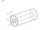
- the present invention can also be applied to a semiconductor ceramic capacitor having a substantially circular tube shape as illustrated in Fig. 3 .
- this semiconductor ceramic capacitor includes a component base 5 having a shape of a substantially circular tube in which a through-hole 6 is formed.
- This component base 5 is composed of the above-described semiconductor ceramic.
- An inner peripheral electrode 7 is formed on the inner peripheral surface of the component base 5, and an outer peripheral electrode 8 is formed on the outer peripheral surface of the component base 5.
- the component base 5 of this semiconductor ceramic capacitor is also composed of the semiconductor ceramic capacitor of the present invention. Accordingly, a semiconductor ceramic capacitor that has good electrical properties and that is suitable for practical use can be obtained, though the diffusing agent does not contain Pb.
- a semiconductor ceramic capacitor having a substantially tubular shape and a large wall thickness has been described.
- the shape of the semiconductor ceramic capacitor is not limited to a substantially tubular shape.
- the present invention can also be effectively applied to a semiconductor ceramic capacitor having other shapes, in particular, having a large thickness.
- grain boundary insulating agents A to D contain Bi 2 O 3 and CuO and do not contain Pb 3 O 4 . Accordingly, grain boundary insulating agents A to D are grain boundary insulating agents within the range of the present invention.
- grain boundary insulating agent E contains 47.5% by weight of Pb 3 O 4 . Accordingly, grain boundary insulating agent E is a grain boundary insulating agent out of the range of the present invention.
- glass raw materials SiO 2 , Li 2 O 3 , M 2 CO 3 (where M represents Sr, Ba, or Ca), TiO 2 , B 2 O 3 , Al 2 O 3 , ZnO, and Bi 2 O 3 were prepared. These glass raw materials were mixed and prepared so as to have the component compositions shown in Table 2. Thus, glass components a to h were prepared.
- glass components a to d are each composed of a SiO 2 -Li 2 O-MO-TiO 2 -based glass material, and do not contain B 2 O 3 or a Pb component. Accordingly, glass components a to d are glass components within the range of the present invention.
- glass components e to h do not contain TiO 2 and contain B 2 O 3 and other components. Accordingly, glass components e to h are glass components out of the range of the present invention.
- Ceramic raw materials SrCO 3 , CaCO 3 , TiO 2 , and Y 2 O 3 were prepared. These ceramic raw materials were weighed so as to have a composition of (Sr 0.795 Ca 0 200 Y 0 005 )TiO 3 . Next, these ceramic raw materials were wet-mixed with a ball mill for 16 hours, and the resulting mixture was dried by evaporation. The mixture was then calcined at a temperature of 1,150°C for two hours to obtain a calcined product, Next, an organic binder, a plasticizer, a dispersant, and water are added to the calcined product, and the resulting mixture was kneaded to prepare a slurry.
- This slurry was charged in a shaping die having a predetermined shape, formed so as to have a tubular shape using an extruder, and dried in a dryer. Subsequently, the dried tube was cut to have a rectangular tube shape. Thus, a formed body was obtained.
- the formed body was fired at a temperature of 400°C to 1,100°C for four hours to remove the organic binder. Next, a firing treatment was performed in a reducing atmosphere of 95% of N 2 and 5% of H 2 at a temperature of 1,400°C to 1,450°C for three hours to obtain a sintered body having a rectangular tube shape.
- the sintered body had a side length of 1.7 mm, an inner diameter of 1.0 mm, and a length of 40 mm.
- diffusing agents were prepared by mixing 0 to 30 parts by weight of one of glass components a to h having the compositions shown in Table 2 with 100 parts by weight of one of grain boundary insulating agents A to E having the compositions shown in Table 1.
- Each of the diffusing agents was weighed so that the amount of diffusing agent was 0.8 to 1.5 parts by weight relative to 100 parts by weight of the sintered body having the rectangular tube shape.
- the diffusing agent was placed in an alumina sagger having a cylindrical shape together with 1,000 sintered bodies.
- the sagger was charged in a rotary heat-treatment furnace and rotated in the heat-treatment furnace.
- heat treatment was performed in air at a temperature of 1,100°C to 1,150°C for two hours while mixing and stirring the sintered bodies and the diffusing agent in the sagger, thereby insulating crystal grain boundaries of the sintered bodies.
- Component bases composed of a grain boundary-insulated semiconductor ceramic were obtained.
- an electrostatic capacity and a dielectric loss of each of the samples of sample Nos. 1 to 43 were measured by applying a voltage of 1 Vrms at a frequency of 1 KHz using a precision LCR meter (4284A manufactured by Agilent Technologies).
- Table 3 shows the composition and the content of the diffusing agents of sample Nos. 1 to 43, and measurement results of the samples of sample Nos. 1 to 43. Note that, of the values of the electrostatic capacity shown in Table 3 is a value converted to an electrostatic capacity per unit length. Table 3 Sample No.
- sample No. 28 Although no glass component was contained, each of the electrical properties was satisfactory. However, grain boundary insulating agent E, which contained a Pb component, was used in sample No. 28.
- sample Nos. 29 to 31 Although grain boundary insulating agent C was used, no glass component was contained in the diffusing agent. Therefore, the electrostatic capacity, the insulation resistance, and the breakdown voltage of sample Nos. 29 to 31 were inferior to those of sample No. 28.
- sample Nos. 34 to 43 glass components e to h, which contained boron (B), were used. As a result, the insulation resistance was decreased to 5,400 M ⁇ or less, and the breakdown voltage was also decreased to 640 V or less. In particular, in sample Nos. 35 to 43, the electrostatic capacity was also decreased to 2,000 pF/mm or less.
- sample Nos. 1 to 27 one of grain boundary insulating agents A to D of the present invention was used, and 3 to 15 parts by weight of one of glass components a to d of the present invention was incorporated relative to 100 parts by weight of the grain boundary insulating agent. Accordingly, the electrostatic capacity of each of these samples was 2,000 pF/mm or more and the breakdown voltage thereof was 890 V or more. Thus, properties substantially the same as or higher than those of sample No. 28, which contained a Pb component, were obtained. The insulation resistance of each of these samples was 8,200 M ⁇ or more. Thus, insulation resistances significantly higher than that of sample No. 28, which contained a Pb component, were obtained.
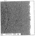
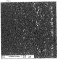
- Fig. 4 is a SEM image of sample No. 11, and Fig. 5 shows the distribution state of Bi of sample No. 11.
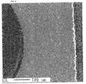
- Fig. 6 is a SEM image of sample No. 38, and Fig. 7 shows the distribution state of Bi of sample No. 38.
- the circular arc portion on the left side shows the inner peripheral surface of the sample, and the substantially linear portion on the right side shows the outer peripheral surface of the sample.
- the SEM images of Figs. 4 and 6 positionally correspond to the distribution states of Bi observed as white spots in Figs. 5 and 7 , respectively.
- Example 1 Slurries were prepared as in Example 1. Next, each of these slurries was charged in a shaping die having a predetermined shape, formed so as to have a tubular shape using an extruder, and dried in a dryer. Subsequently, the dried tube was cut to have a circular tube shape. Thus, a formed body was obtained. Thereafter, a sintered body having a circular tube shape was obtained by the same method and procedure as in Example 1. The sintered body had an outer diameter of 3.0 mm, an inner diameter of 1.6 mm, and a length of 2.5 mm.
- diffusing agents were prepared by mixing 0 to 15 parts by weight of one of glass components a to d with 100 parts by weight of one of grain boundary insulating agents A to E.
- Each of the diffusing agents was weighed so that the amount of diffusing agent was 1.0 part by weight relative to 100 parts by weight of the sintered body having the circular tube shape.
- the diffusing agent was placed in an alumina sagger having a cylindrical shape together with 1,000 sintered bodies.
- the sagger was charged in a rotary heat-treatment furnace and rotated in the heat-treatment furnace.
- heat treatment was performed in air at a temperature of 1,100°C to 1,150°C for two hours white mixing and stirring the sintered bodies and the diffusing agent in the sagger, thereby insulating crystal grain boundaries of the sintered bodies.
- Component bases composed of a grain boundary-insulated semiconductor ceramic were obtained.
- Electrodes were then formed on the inner peripheral surface and the outer peripheral surface of each of the component bases by the same method and procedure as in Example 1 to prepare samples of sample Nos. 51 to 65.
- Table 4 shows the composition and the content of the diffusing agents of sample Nos. 51 to 65, and measurement results of the samples of sample Nos. 51 to 65.
- Table 4 Sample No. Diffusing agent Electrical properties Content relative to 100 parts by weight of main component (parts by weight) Grain boundary insulating agent Glass component Electrostatic capacity (nF) Dielectric loss (%) Insulation resistance (M ⁇ ) Breakdown voltage (V) Composition Composition Content relative to 100 parts by weight of grain boundary insulating agent (parts by weight) 51 1.0 A c 5 5.1 1.2 38,000 1,800 52 1.0 A c 8 5.1 1.3 41,000 1,900 53 1.0 B b 5 5.1 0.9 42,000 2,000 54 1.0 B b 8 5.0 0.8 45,000 2,100 55 1.0 C a 3 5.1 0.8 40,000 1,800 56 1.0 C b 5 5.1 0.8 42,000 2,000 57 1.0 C c 5 5.1 0.7 45,000 2,100 58 1.0 C d 5 5.1 0.8 42,000 1,900 59 1.0 C c 3
- sample No. 64 Although no glass component was contained, each of the electrical properties was satisfactory. However, grain boundary insulating agent E, which contained a Pb component, was used in sample No. 64.
- sample No. 65 Although grain boundary insulating agent C was used, no glass component was contained in the diffusing agent. Therefore, the electrostatic capacity, the insulation resistance, and the breakdown voltage of sample No. 65 were inferior to those of sample No. 64.
- sample Nos. 51 to 63 one of grain boundary insulating agents A to D of the present invention was used, and 3 to 15 parts by weight of one of glass components a to d of the present invention was incorporated relative to 100 parts by weight of the grain boundary insulating agent. Accordingly, the electrostatic capacity of each of these samples was 5.0 to 5.1 nF and the breakdown voltage thereof was 1,800 to 2,200 V. Thus, properties substantially the same as or higher than those of sample No. 64, which contained a Pb component, were obtained. The insulation resistance of each of these samples was 38,000 to 50,000 M ⁇ . Thus, insulation resistances significantly higher than that of sample No. 64 were obtained.
Landscapes
- Engineering & Computer Science (AREA)
- Chemical & Material Sciences (AREA)
- Ceramic Engineering (AREA)
- Power Engineering (AREA)
- Manufacturing & Machinery (AREA)
- Materials Engineering (AREA)
- Organic Chemistry (AREA)
- Inorganic Chemistry (AREA)
- Microelectronics & Electronic Packaging (AREA)
- General Chemical & Material Sciences (AREA)
- Geochemistry & Mineralogy (AREA)
- Chemical Kinetics & Catalysis (AREA)
- Life Sciences & Earth Sciences (AREA)
- Dispersion Chemistry (AREA)
- Structural Engineering (AREA)
- Ceramic Capacitors (AREA)
- Inorganic Insulating Materials (AREA)
- Compositions Of Oxide Ceramics (AREA)
Abstract
Description
- The invention relates to a grain boundary-insulated semiconductor ceramic, a semiconductor ceramic capacitor, and a method for producing a semiconductor ceramic capacitor. More specifically, the present invention relates to a grain boundary-insulated semiconductor ceramic containing SrTiO3 as a main component and a diffusing agent that contains a grain boundary insulating agent and a glass component, a semiconductor ceramic capacitor including the grain boundary-insulated semiconductor ceramic, and a method for producing the semiconductor ceramic capacitor.
- Grain boundary-insulated semiconductor ceramic capacitors are capacitors in which the apparent dielectric constant is increased by forming semiconductor crystal grains and insulating crystal grain boundaries, and are widely known as capacitors having small sizes and large capacitances.
- For example, Japanese Unexamined Patent Application Publication No.
3-285870 - In
JP 3-285870 - Japanese Unexamined Patent Application Publication No.
2-111006 - In
JP 2-111006 - Recently, the consciousness of environmental issues has been increasing worldwide. In particular, in the European Union (EU), regulation of the use of lead (Pb), which causes environmental pollution, has been prepared by, for example, the Restriction of Hazardous Substances (RoHS) that prescribes the restriction of the use of certain hazardous substances in electrical and electronic equipment and the End of Life Vehicles Directive (ELV) that prescribes the environmental regulation of end-of-life vehicles. Accordingly, development of materials alternative to Pb-based materials has been urgently required.
- However, in
JP 3-285870 JP 3-285870 - In
JP 2-111006 JP 3-285870 JP2-111006 - We have therefore appreciated that it would be desirable to provide a grain boundary-insulated semiconductor ceramic in which good electrical properties can be obtained without using a Pb-based material as a diffusing agent, a semiconductor ceramic capacitor including the grain boundary-insulated semiconductor ceramic, and a method for producing the semiconductor ceramic capacitor.
- A grain boundary-insulated semiconductor ceramic according to a preferred embodiment of the present invention includes a SrTiO3-based compound as a main component, and a diffusing agent containing a grain boundary insulating agent and a glass component, wherein the grain boundary insulating agent is composed of a non-lead material free of lead, the glass component mainly contains a SiO2-X2O-MO-TiO2-based glass material that does not contain boron or lead (where X represents an alkali metal, and M represents at least one selected from barium, strontium, and calcium), and the content of the glass component is 3 to 15 parts by weight relative to 100 parts by weight of the grain boundary insulating agent.
- The grain boundary insulating agent preferably contains at least bismuth and copper.
- The content of the grain boundary insulating agent is preferably 0.8 to 1.5 parts by weight relative to 100 parts by weight of the main component,
- Furthermore, the alkali metal X in the glass component is preferably lithium.
- A semiconductor ceramic capacitor according to a preferred embodiment of the present invention includes a component base composed of any of the above grain boundary-insulated semiconductor ceramics.
- The component base preferably has a tubular shape, and an electrode is preferably provided on each of an inner peripheral surface and an outer peripheral surface of the component base.
- A method for producing a semiconductor ceramic capacitor according to a preferred embodiment of the present invention includes the steps of preparing a sintered body by mixing a plurality of ceramic raw materials including at least a strontium compound and a titanium compound and firing the resulting mixture in a reducing atmosphere, weighing a grain boundary insulating agent composed of a non-lead material free of lead and a glass component composed of a SiO2-X2O-MO-TiO2-based glass material that does not contain boron or lead (where X represents an alkali metal, and M represents at least one selected from barium, strontium, and calcium), and preparing a component base by performing heat treatment in an air atmosphere while mixing and stirring the sintered body with the grain boundary insulating agent and the glass component.
- In the method, the sintered body is preferably prepared so as to have a tubular shape, and the method preferably further includes a step of forming an electrode on each of an inner peripheral surface and an outer peripheral surface of the component base by a plating process.
- Furthermore, in the method, the grain boundary insulating agent and the glass component are preferably weighed so that the amount of the glass component is 3 to 15 parts by weight relative to 100 parts by weight of the grain boundary insulating agent.
- According the grain boundary-insulated semiconductor ceramic according to a preferred embodiment of the present invention, the grain boundary insulating agent is composed of a non-Pb material free of Pb, such as a Bi-Cu-based material, and the glass component contains, as a main component, a SiO2-X2O-MO-TiO2-based glass material that does not contain B or Pb (where X represents an alkali metal such as Li, and M represents at least one selected from Ba, Sr, and Ca), and the content of the glass component is 3 to 15 parts by weight relative to 100 parts by weight of the grain boundary insulating agent. Accordingly, even though Pb is not contained, it is possible to obtain a grain boundary-insulated semiconductor ceramic having electrical properties equal to or better than those in the case where a Pb-based diffusing agent is used without causing a decrease in the insulation resistance or the breakdown voltage.
- According to the semiconductor ceramic capacitor according to a preferred embodiment of the present invention, a component base is composed of the above-described grain boundary-insulated semiconductor ceramic. Accordingly, even in the case where a non-Pb material is used as a semiconductor ceramic, a semiconductor ceramic capacitor having good electrical properties can be obtained.
- Furthermore, the component base is formed so as to have a tubular shape, and an electrode is formed on each of the inner peripheral surface and the outer peripheral surface of the component base, and thus the diffusing agent is uniformly or substantially uniformly distributed over the entire component base. Therefore, even in the case where the component base has a large wall thickness, it is possible to obtain a semiconductor ceramic capacitor that has good electrical properties such as the electrostatic capacity, the insulation resistance, and the breakdown voltage and that is excellent in terms of practical use.
- The method for producing a semiconductor ceramic capacitor according to a preferred embodiment of the present invention includes the steps of preparing a sintered body by mixing a plurality of ceramic raw materials including at least a strontium compound and a titanium compound and firing the resulting mixture in a reducing atmosphere, weighing a grain boundary insulating agent composed of a non-lead material free of lead and a glass component composed of a SiO2-X2O-MO-TiO2-based glass material that does not contain boron or lead (where X represents an alkali metal, and M represents at least one selected from barium, strontium, and calcium), and preparing a component base by performing heat treatment in an air atmosphere while mixing and stirring the sintered body with the grain boundary insulating agent and the glass component. Accordingly, the diffusing agent containing the grain boundary insulating agent and the glass component has a diffusing power substantially the same as that of a lead-based diffusing agent. Therefore, even when a sintered body has a tubular shape having a large wall thickness, the diffusing agent can be uniformly or substantially uniformly distributed in the component base. Thus, grain boundaries can be uniformly oxidized, and a desired grain boundary insulating layer can be formed. The semiconductor ceramic capacitor thus obtained has good electrical properties such as the electrostatic capacity, the insulation resistance, and the breakdown voltage, and is excellent in terms of practical use.
- Features, elements, characteristics and advantages of the present invention will become more apparent from the following detailed description of preferred embodiments of the present invention with reference to the attached drawings.
-
Fig. 1 is a perspective view that schematically illustrates an embodiment (first embodiment) of a semiconductor ceramic capacitor obtained using a grain boundary-insulated semiconductor ceramic of the present invention; -
Fig. 2 is a longitudinal cross-sectional view ofFig. 1 ; -
Fig. 3 is a perspective view that schematically illustrates a second embodiment of a semiconductor ceramic capacitor; -
Fig. 4 is a scanning electron microscope (SEM) image of sample No. 11 of Example 1; -
Fig. 5 is a photograph showing the distribution state of bismuth (Bi) of sample No. 11 of Example 1; -
Fig. 6 is a STEM image of sample No. 38 of Example 1; and -
Fig. 7 is a photograph showing the distribution state of Bi of sample No. 38 of Example 1. - The inventor of the present invention has conducted intensive studies in order to achieve the above object. As a result, it was found that, by using a non-Pb material free of Pb, such as a Bi-Cu-based material, as a grain boundary insulating agent and using a SiO2-X2O-MO-TiO2-based glass material that does not contain B or Pb (where X represents an alkali metal and M represents at least one selected from Ba, Sr, and Ca) as a glass component, a grain boundary-insulated semiconductor ceramic having good electrical properties can be obtained without decreasing the insulation resistance or the breakdown voltage, even though a diffusing agent is composed of a non-Pb material.
- Embodiments of the present invention will now be described in detail.
-
Fig. 1 is a perspective view that schematically illustrates an embodiment of a semiconductor ceramic capacitor obtained using a grain boundary-insulated semiconductor ceramic of the present invention.Fig. 2 is a longitudinal cross-sectional view ofFig. 1 . - The semiconductor ceramic capacitor includes a
component base 2 which has a shape of a substantially rectangular tube and in which a through-hole 1 is formed. An innerperipheral electrode 3 is formed on the inner peripheral surface of thecomponent base 2, and an outerperipheral electrode 4 is formed on the outer peripheral surface of thecomponent base 2. - For example, this semiconductor ceramic capacitor is sandwiched and fixed between a pair of inductance elements such as ferrite beads, and widely used as a noise filter.
- The
component base 2 is specifically composed of a grain boundary-insulated semiconductor ceramic. This grain boundary-insulated semiconductor ceramic is made up of an aggregate containing semiconductor crystal grains and a grain boundary insulating layer formed around the crystal grains. The crystal grains form an electrostatic capacity with the grain boundary insulating layer therebetween, - The grain boundary-insulated semiconductor ceramic contains a SrTiO3-based material as a main component and a diffusing agent as an accessory component. In the grain boundary-insulated semiconductor ceramic, semiconductor crystal grains are formed by a firing treatment in a reducing atmosphere, and a metal oxide is thermally diffused from the surfaces of the crystal grains by heat treatment performed after the firing treatment so that crystal grain boundaries are oxidized and insulated. Thus, a grain boundary insulating layer is formed.
- The diffusing agent contains a grain boundary insulating agent that contributes to insulate crystal grain boundaries and a glass component that functions as a thermal diffusion promoting agent.
- A non-Pb material free of Pb is used as the grain boundary insulating agent. Since Pb causes environmental pollution, Pb is eliminated from this grain boundary insulating agent in order to reduce the environmental burden.
- The grain boundary insulating agent is not particularly limited as long as the grain boundary insulating agent is composed of a non-Pb material and forms a desired grain boundary insulating layer by thermal diffusion. However, from the standpoint of obtaining electrical properties equal to or better than those obtained in the case where a Pb-based material is used, a metal oxide containing at least Bi and Cu is preferably used as the grain boundary insulating agent.
- The glass component contains, as a main component, a SiO2-X2O-MO-TiO2-based glass material that does not contain B or Pb. In the above formula, X represents an alkali metal, and typical examples of the alkali metal include Li, Na, and K. Among these alkali metals X, Li is preferably used. In the above formula, M represents at least one selected from Ba, Sr, and Ca.
- As in the case of the grain boundary insulating agent, since Pb causes environmental pollution, Pb is eliminated from this glass component in order to reduce the environmental burden. The reason why B is eliminated from the glass component is as follows: In the case of borosilicate glass containing B as a glass component, although the diffusing power can be improved to a certain degree, the insulation resistance and the breakdown voltage tend to decrease. Consequently, electrical properties may decrease as compared with the case where a Pb-based diffusing agent is used.
- The glass component is incorporated so that the content of the glass component is about 3 to 15 parts by weight relative to 100 parts by weight of the grain boundary insulating agent. When the content of the glass component is less than about 3 parts by weight relative to 100 parts by weight of the grain boundary insulating agent, electrical properties such as the electrostatic capacity, the insulation resistance, and the breakdown voltage may degrade. On the other hand, when the content of the glass component exceeds about 15 parts by weight relative to 100 parts by weight of the grain boundary insulating agent, although a satisfactory insulation resistance and breakdown voltage are obtained, the electrostatic capacity may decrease, and
component base 2 may adhere to each other during the heat treatment. - Accordingly, in order to ensure desired electrical properties, it is necessary to incorporate the glass component in an amount of about 3 to 15 parts by weight relative to 100 parts by weight of the grain boundary insulating agent.
- As described above, in this embodiment, the grain boundary insulating agent is composed of a non-Pb material free of Pb, such as a Bi-Cu-based material, the glass component contains, as a main component, a SiO2-X2O-MO-TiO2-based glass material that does not contain B or Pb, and the content of the glass component is about 3 to 15 parts by weight relative to 100 parts by weight of the grain boundary insulating agent. Therefore, even though Pb is not contained, it is possible to obtain a grain boundary-insulated semiconductor ceramic having electrical properties equal to or better than those obtained in the case where a Pb-based diffusing agent is used without causing a decrease in the insulation resistance or the breakdown voltage.
- The present invention is particularly effective in a semiconductor ceramic capacitor having a substantially tubular shape.
- Specifically, in the case where the semiconductor ceramic capacitor has a substantially thin-plate shape such as a substantially disc shape, a metal oxide on the surfaces of crystal grains can easily thermally diffuse to form a desired a grain boundary insulating layer.
- In the case where the
component base 2 is formed so as to have a substantially tubular shape such as a substantially rectangular tube, as illustrated inFigs. 1 and2 , thecomponent base 2 may have a large thickness between the inner peripheral surface and the outer peripheral surface thereof, that is, a large wall thickness of about 100 µm or more, for example. In the case where thecomponent base 2 has a large wall thickness and is free of Pb, which is excellent in terms of diffusibility, it has been hitherto difficult to form a satisfactory grain boundary insulating layer. - However, according to the present invention, even when the
component base 2 has a large wall thickness, a metal oxide on the surfaces of crystal grains can be easily thermally diffused, and a semiconductor ceramic capacitor having desired electrical properties can be obtained without causing environmental pollution. - The semiconductor ceramic is not particularly limited as long as the semiconductor ceramic contains SrTiO3 as a main component. For example, some of the Sr atoms may be replaced with Ba and/or Ca atoms. It is also preferable to incorporate a rare-earth element such as Y, La, or Sm in order to facilitate the formation of a semiconductor during the firing treatment. The molar ratio of the Sr site and the Ti site is 1.000 in terms of stoichiometric composition. However, it is also preferable to mix a Sr compound and a Ti compound as required so that the semiconductor ceramic has a Sr-site-rich composition or a Ti-site-rich composition. Furthermore, it is also preferable to incorporate various additives as required in order to obtain desired electrical properties according to the use of the semiconductor ceramic.
- The electrode materials of the inner
peripheral electrode 3 and the outerperipheral electrode 4 are also not particularly limited. For example, a Ni-Sn alloy or a Ni-Cu alloy can be used. Each of the electrodes may be formed so as to have a two-layer structure by a plating method using these metal materials. - Next, a method for producing the semiconductor ceramic capacitor will be described in detail.
- As ceramic raw materials, a Sr compound and a Ti compound, as required, a Ca compound, a Ba compound, a rare-earth element compound, and the like are prepared. Predetermined amounts of these ceramic raw materials are weighed. The ceramic raw materials are then sufficiently wet-mixed with a ball mill, and the resulting mixture is dried by evaporation. Subsequently, the mixture is calcined at a temperature of about 1,100°C to 1,300°C for about two hours to obtain a calcined product.
- Next, an organic binder, a plasticizer, a dispersant, and water are added to the calcined product, and the resulting mixture is kneaded to prepare a slurry. Next, this slurry is charged in a shaping die having a predetermined shape, formed so as to have a substantially tubular shape using an extruder or the like, and dried in a dryer. Subsequently, the dried tube is cut to have a substantially rectangular tube shape. Thus, a formed body is obtained. The formed body is fired at a temperature of about 400°C to 1,100°C for about four hours to remove the organic binder. Next, a firing treatment is performed in a reducing atmosphere of about 90% to 97% of N2 and about 3% to 10% of H2 at a temperature of about 1,400°C to 1,500°C for about three hours to obtain a sintered body having a substantially rectangular tube shape.
- Next, a grain boundary insulating agent composed of a non-Pb material free of Pb, for example, a material containing Bi2O3 and CuO is prepared. is Furthermore, a SiO2-X2O-MO-TiO2-based glass material that does not contain B or Pb is prepared as a glass component.
- The grain boundary insulating agent and the glass component are mixed so that the content of the glass component is about 3 to 15 parts by weight relative to 100 parts by weight of the grain boundary insulating agent to prepare a diffusing agent.
- Next, the diffusing agent is charged in a rotary heat-treatment furnace together with the sintered body. Heat treatment is performed in air at a temperature of about 1,100°C to 1,200°C for about two hours while mixing and stirring the sintered body and the diffusing agent so as to insulate crystal grain boundaries of the sintered body. Thus, a
component base 2 composed of a grain boundary-insulated semiconductor ceramic is prepared. A ratio of the diffusing agent to the sintered body is not particularly limited. However, for example, the diffusing agent is mixed so that the amount of diffusing agent is about 0.8 to 1.5 parts by weight relative to 100 parts by weight of the sintered body. - Next, at least one plating film is formed on each of the inner peripheral surface and the outer peripheral surface of the
component base 2 by electroless plating and/or electrolytic plating, thereby forming an innerperipheral electrode 3 and an outerperipheral electrode 4. Thus, a semiconductor ceramic capacitor is prepared. - As described above, according to the present embodiment, the method for producing a semiconductor ceramic capacitor includes the steps of preparing a sintered by mixing ceramic raw materials including a Sr compound and a Ti compound and firing the resulting mixture in a reducing atmosphere, weighing a grain boundary insulating agent composed of a non-Pb material free of Pb and a glass component composed of a SiO2-X2O-MO-TiO2-based glass material that does not contain B or Pb, and preparing a
component base 2 by performing heat treatment in an air atmosphere while mixing and stirring the sintered body with the grain boundary insulating agent and the glass component. Accordingly, even when the sintered body has a substantially tubular shape having a large wall thickness, the diffusing agent can be uniformly or substantially uniformly distributed in thecomponent base 2. Thus, crystal grain boundaries can be uniformly oxidized, and a desired grain boundary insulating layer can be obtained. The semiconductor ceramic capacitor thus obtained has good electrical properties such as the electrostatic capacity, the insulation resistance, and the breakdown voltage, and is excellent in terms of practical use. - The present invention is not limited to the above embodiment. In the above embodiment, a semiconductor ceramic capacitor having a substantially rectangular tube shape has been described. However, for example, the present invention can also be applied to a semiconductor ceramic capacitor having a substantially circular tube shape as illustrated in
Fig. 3 . - Specifically, this semiconductor ceramic capacitor includes a component base 5 having a shape of a substantially circular tube in which a through-
hole 6 is formed. This component base 5 is composed of the above-described semiconductor ceramic. An inner peripheral electrode 7 is formed on the inner peripheral surface of the component base 5, and an outer peripheral electrode 8 is formed on the outer peripheral surface of the component base 5. - The component base 5 of this semiconductor ceramic capacitor is also composed of the semiconductor ceramic capacitor of the present invention. Accordingly, a semiconductor ceramic capacitor that has good electrical properties and that is suitable for practical use can be obtained, though the diffusing agent does not contain Pb.
- In the above embodiments, a semiconductor ceramic capacitor having a substantially tubular shape and a large wall thickness has been described. However, the shape of the semiconductor ceramic capacitor is not limited to a substantially tubular shape. The present invention can also be effectively applied to a semiconductor ceramic capacitor having other shapes, in particular, having a large thickness.
- Next, Examples of the present invention will be specifically described.
- As insulating raw materials, BiO3, CuO, and Pb3O4 were prepared. These insulating raw materials were mixed and prepared so as to have the component compositions shown in Table 1. Thus, grain boundary insulating agents A to E were prepared.
Table 1 Type of grain boundary insulating agent Component composition (wt%) Bi2O3 CuO Pb3O4 A 85 15 - B 90 10 - C 95 5 - D 98 2 - E* 47.5 5 47.5 * Out of the range of the present invention - As is apparent from Table 1, grain boundary insulating agents A to D contain Bi2O3 and CuO and do not contain Pb3O4. Accordingly, grain boundary insulating agents A to D are grain boundary insulating agents within the range of the present invention.
- In contrast, grain boundary insulating agent E contains 47.5% by weight of Pb3O4. Accordingly, grain boundary insulating agent E is a grain boundary insulating agent out of the range of the present invention.
- Next, as glass raw materials, SiO2, Li2O3, M2CO3 (where M represents Sr, Ba, or Ca), TiO2, B2O3, Al2O3, ZnO, and Bi2O3 were prepared. These glass raw materials were mixed and prepared so as to have the component compositions shown in Table 2. Thus, glass components a to h were prepared.
Table 2 Type of glass component Component composition (mol%) SiO2 Li2O MO TiO2 B2O3 Al2O3 ZnO Bi2O3 M Content (mol%) a 50 15 Sr 27 8 - - - - b 46 24 Ba/Sr 10/10 10 - - - - c 48 30 Ba/Sr/Ca 8/6/5 3 - - - - d 40 36 Sr/Ca 8/10 6 - - - - e* 30 8 Ba/ Ca 6/36 - 20 - - - f* 43 - Ca 43 - 8 6 - g* 35 10 Ca 13 - 24 - 9 9 h* 12 - Ba/Ca 10/20 - 30 - 25 3 - As is apparent from Table 2, glass components a to d are each composed of a SiO2-Li2O-MO-TiO2-based glass material, and do not contain B2O3 or a Pb component. Accordingly, glass components a to d are glass components within the range of the present invention.
- In contrast, glass components e to h do not contain TiO2 and contain B2O3 and other components. Accordingly, glass components e to h are glass components out of the range of the present invention.
- As ceramic raw materials, SrCO3, CaCO3, TiO2, and Y2O3 were prepared. These ceramic raw materials were weighed so as to have a composition of (Sr0.795Ca0 200Y0 005)TiO3. Next, these ceramic raw materials were wet-mixed with a ball mill for 16 hours, and the resulting mixture was dried by evaporation. The mixture was then calcined at a temperature of 1,150°C for two hours to obtain a calcined product, Next, an organic binder, a plasticizer, a dispersant, and water are added to the calcined product, and the resulting mixture was kneaded to prepare a slurry. This slurry was charged in a shaping die having a predetermined shape, formed so as to have a tubular shape using an extruder, and dried in a dryer. Subsequently, the dried tube was cut to have a rectangular tube shape. Thus, a formed body was obtained. The formed body was fired at a temperature of 400°C to 1,100°C for four hours to remove the organic binder. Next, a firing treatment was performed in a reducing atmosphere of 95% of N2 and 5% of H2 at a temperature of 1,400°C to 1,450°C for three hours to obtain a sintered body having a rectangular tube shape. The sintered body had a side length of 1.7 mm, an inner diameter of 1.0 mm, and a length of 40 mm.
- Next, diffusing agents were prepared by mixing 0 to 30 parts by weight of one of glass components a to h having the compositions shown in Table 2 with 100 parts by weight of one of grain boundary insulating agents A to E having the compositions shown in Table 1.
- Each of the diffusing agents was weighed so that the amount of diffusing agent was 0.8 to 1.5 parts by weight relative to 100 parts by weight of the sintered body having the rectangular tube shape. The diffusing agent was placed in an alumina sagger having a cylindrical shape together with 1,000 sintered bodies. The sagger was charged in a rotary heat-treatment furnace and rotated in the heat-treatment furnace. Thus, heat treatment was performed in air at a temperature of 1,100°C to 1,150°C for two hours while mixing and stirring the sintered bodies and the diffusing agent in the sagger, thereby insulating crystal grain boundaries of the sintered bodies. Component bases composed of a grain boundary-insulated semiconductor ceramic were obtained.
- Subsequently, a nickel film was formed on each of the inner peripheral surface and the outer peripheral of each of the component bases by electroless nickel plating. A tin film was further formed on the surface of the nickel film by electrolytic tin plating to form electrodes each having a two-layer structure. Thus, semiconductor ceramic capacitors of sample Nos. 1 to 43 were prepared.
- Next, an electrostatic capacity and a dielectric loss of each of the samples of sample Nos. 1 to 43 were measured by applying a voltage of 1 Vrms at a frequency of 1 KHz using a precision LCR meter (4284A manufactured by Agilent Technologies).
- An insulation resistance and a breakdown voltage of each of the samples of sample Nos. 1 to 43 were measured by applying a voltage of 250 V using a digital ultrahigh resistance/micro current meter (R8340A manufactured by Advantest Corporation).
- Table 3 shows the composition and the content of the diffusing agents of sample Nos. 1 to 43, and measurement results of the samples of sample Nos. 1 to 43. Note that, of the values of the electrostatic capacity shown in Table 3 is a value converted to an electrostatic capacity per unit length.
Table 3 Sample No. Diffusing agent Electrical properties Content relative to 100 parts by weight of main component (parts by weight) Grain boundary insulating agent Glass component Electrostatic capacity (pF/mm) Dielectric loss (%) Insulation resistance (MΩ) Breakdown voltage (V) Composition Composition Content relative to 100 parts by weight of grain boundary insulating agent (parts by weight) 1 0.8 C b 3 2,060 0.2 8,200 890 2 0.8 C b 5 2,010 0.3 9,100 900 3 0.8 C b 10 2,040 0.3 9,600 920 4 0.8 C b 15 2,040 0.3 10,000 930 5 0.8 C c 5 2,050 0.3 11,000 920 6 1.0 A a 5 2,040 0.5 8,200 900 7 1.0 A d 5 2,020 0.6 8,400 910 8 1.0 B b 5 2,050 0.3 9,300 920 9 1.0 B c 5 2,050 0.3 9,800 940 10 1.0 C c 3 2,040 0.2 8,600 900 11 1.0 C a 5 2,060 0.3 10,000 950 12 1.0 C b 5 2,050 0.3 13,000 980 13 1.0 C c 5 2,060 0.3 14,000 1,080 14 1.0 C d 5 2,040 0.2 13,000 1,000 15 1.0 C c 10 2,040 0.3 15,000 1,150 16 1.0 C c 15 2,000 0.3 14,000 1,000 17 1.0 D a 5 2,020 0.3 10,000 910 18 1.0 D d 5 2,050 0.2 12,000 970 19 1.2 B b 5 2,000 0.6 10,000 930 20 1.2 B c 5 2,000 0.6 9,400 900 21 1.2 C b 3 2,030 0.3 8,800 890 22 1.2 C b 5 2,010 0.3 9,200 950 23 1.5 C b 3 2,030 0.3 8,900 900 24 1.5 C b 5 2,020 0.4 11,000 960 25 1.5 C b 10 2,020 0.4 12,000 1,020 26 1.5 C b 15 2,000 0.4 12,000 980 27 1.5 C c 5 2,000 0.3 14,000 1,000 28* 1.2 E - 0 2,050 0.3 7,000 880 29* 1.0 C - 0 1,970 0.3 1,400 460 30* 1.2 C - 0 1,980 0.3 3,000 540 31* 1.5 C - 0 1,970 0.3 3,100 550 32* 1.0 C b 20 1,940 0.4 15,000 1,120 33* 1.0 C b 30 1,910 0.4 14,000 1,100 34* 1.0 C e 3 2,010 0.4 5,000 620 35* 1.0 C f 3 1,970 0.3 5,400 640 36* 1.0 C g 3 1,970 0.3 4,500 600 37* 1.0 C h 3 1,980 0.3 4,800 620 38* 1.0 C e 5 1,990 0.3 3,500 550 39* 1.0 C f 5 1,940 0.3 3,900 580 40* 1.0 C g 5 1,920 0.3 2,600 510 41* 1.0 C h 5 1,940 0.4 3,000 560 42* 1.0 C f 10 1,910 0.4 1,800 510 43* 1.0 C g 10 1,910 0.3 1,200 400 * Out of the range of the present invention - In sample No. 28, although no glass component was contained, each of the electrical properties was satisfactory. However, grain boundary insulating agent E, which contained a Pb component, was used in sample No. 28.
- In sample Nos. 29 to 31, although grain boundary insulating agent C was used, no glass component was contained in the diffusing agent. Therefore, the electrostatic capacity, the insulation resistance, and the breakdown voltage of sample Nos. 29 to 31 were inferior to those of sample No. 28.
- In sample Nos. 32 and 33, the content of the glass component was large, i.e., 20 to 30 by weight relative to 100 by weight of the grain boundary insulating agent, Therefore, the electrostatic capacities of these samples were decreased to 2,000 pF/mm or less.
- In sample Nos. 34 to 43, glass components e to h, which contained boron (B), were used. As a result, the insulation resistance was decreased to 5,400 MΩ or less, and the breakdown voltage was also decreased to 640 V or less. In particular, in sample Nos. 35 to 43, the electrostatic capacity was also decreased to 2,000 pF/mm or less.
- In contrast, in sample Nos. 1 to 27, one of grain boundary insulating agents A to D of the present invention was used, and 3 to 15 parts by weight of one of glass components a to d of the present invention was incorporated relative to 100 parts by weight of the grain boundary insulating agent. Accordingly, the electrostatic capacity of each of these samples was 2,000 pF/mm or more and the breakdown voltage thereof was 890 V or more. Thus, properties substantially the same as or higher than those of sample No. 28, which contained a Pb component, were obtained. The insulation resistance of each of these samples was 8,200 MΩ or more. Thus, insulation resistances significantly higher than that of sample No. 28, which contained a Pb component, were obtained.
- Next, cross-sectional images of sample Nos. 11 and 38 were taken with a scanning electron microscope (hereinafter referred to as "SEM"), and the distribution state of bismuth (Bi) on the cross section was observed by wavelength dispersive X-ray spectroscopy (WDX).
-
Fig. 4 is a SEM image of sample No. 11, andFig. 5 shows the distribution state of Bi of sample No. 11.Fig. 6 is a SEM image of sample No. 38, andFig. 7 shows the distribution state of Bi of sample No. 38. InFigs. 4 and6 , the circular arc portion on the left side shows the inner peripheral surface of the sample, and the substantially linear portion on the right side shows the outer peripheral surface of the sample. The SEM images ofFigs. 4 and6 positionally correspond to the distribution states of Bi observed as white spots inFigs. 5 and7 , respectively. - As is apparent from
Figs. 6 and7 , in sample No. 38, which was out of the range of the present invention, bismuth diffused from the outer surface did not sufficiently diffuse in the component base up to the inner peripheral surface. - In contrast, as is apparent from
Figs. 4 and5 , it was confirmed that, in sample No. 11, which was within the range of the present invention, bismuth diffused from the outer surface substantially uniformly diffused in the component base up to the inner peripheral surface. - Slurries were prepared as in Example 1. Next, each of these slurries was charged in a shaping die having a predetermined shape, formed so as to have a tubular shape using an extruder, and dried in a dryer. Subsequently, the dried tube was cut to have a circular tube shape. Thus, a formed body was obtained. Thereafter, a sintered body having a circular tube shape was obtained by the same method and procedure as in Example 1. The sintered body had an outer diameter of 3.0 mm, an inner diameter of 1.6 mm, and a length of 2.5 mm.
- Next, diffusing agents were prepared by mixing 0 to 15 parts by weight of one of glass components a to d with 100 parts by weight of one of grain boundary insulating agents A to E.
- Each of the diffusing agents was weighed so that the amount of diffusing agent was 1.0 part by weight relative to 100 parts by weight of the sintered body having the circular tube shape. The diffusing agent was placed in an alumina sagger having a cylindrical shape together with 1,000 sintered bodies. The sagger was charged in a rotary heat-treatment furnace and rotated in the heat-treatment furnace. Thus, heat treatment was performed in air at a temperature of 1,100°C to 1,150°C for two hours white mixing and stirring the sintered bodies and the diffusing agent in the sagger, thereby insulating crystal grain boundaries of the sintered bodies. Component bases composed of a grain boundary-insulated semiconductor ceramic were obtained.
- Electrodes were then formed on the inner peripheral surface and the outer peripheral surface of each of the component bases by the same method and procedure as in Example 1 to prepare samples of sample Nos. 51 to 65.
- Subsequently, the electrostatic capacity, the dielectric loss, the insulation resistance, and the breakdown voltage of each of the samples of sample Nos. 51 to 65 were measured by the same method and procedure as in Example 1.
- Table 4 shows the composition and the content of the diffusing agents of sample Nos. 51 to 65, and measurement results of the samples of sample Nos. 51 to 65.
Table 4 Sample No. Diffusing agent Electrical properties Content relative to 100 parts by weight of main component (parts by weight) Grain boundary insulating agent Glass component Electrostatic capacity (nF) Dielectric loss (%) Insulation resistance (MΩ) Breakdown voltage (V) Composition Composition Content relative to 100 parts by weight of grain boundary insulating agent (parts by weight) 51 1.0 A c 5 5.1 1.2 38,000 1,800 52 1.0 A c 8 5.1 1.3 41,000 1,900 53 1.0 B b 5 5.1 0.9 42,000 2,000 54 1.0 B b 8 5.0 0.8 45,000 2,100 55 1.0 C a 3 5.1 0.8 40,000 1,800 56 1.0 C b 5 5.1 0.8 42,000 2,000 57 1.0 C c 5 5.1 0.7 45,000 2,100 58 1.0 C d 5 5.1 0.8 42,000 1,900 59 1.0 C c 3 5.1 0.8 41,000 1,800 60 1.0 C c 8 5.1 0.7 50,000 2,200 61 1.0 C c 15 5.0 0.8 46,000 2,000 62 1.0 D c 3 5.1 0.8 40,000 1,900 63 1.0 D c 5 5.1 0.9 42,000 2,000 64* 1.0 E - 0 5.1 0.8 33,000 1,600 65* 1.0 C - 0 4.6 0.7 21,000 1,000 * Out of the range of the present invention - In sample No. 64, although no glass component was contained, each of the electrical properties was satisfactory. However, grain boundary insulating agent E, which contained a Pb component, was used in sample No. 64.
- In sample No. 65, although grain boundary insulating agent C was used, no glass component was contained in the diffusing agent. Therefore, the electrostatic capacity, the insulation resistance, and the breakdown voltage of sample No. 65 were inferior to those of sample No. 64.
- In contrast, in sample Nos. 51 to 63, one of grain boundary insulating agents A to D of the present invention was used, and 3 to 15 parts by weight of one of glass components a to d of the present invention was incorporated relative to 100 parts by weight of the grain boundary insulating agent. Accordingly, the electrostatic capacity of each of these samples was 5.0 to 5.1 nF and the breakdown voltage thereof was 1,800 to 2,200 V. Thus, properties substantially the same as or higher than those of sample No. 64, which contained a Pb component, were obtained. The insulation resistance of each of these samples was 38,000 to 50,000 MΩ. Thus, insulation resistances significantly higher than that of sample No. 64 were obtained.
- As described above, it is possible to realize a grain boundary-insulated semiconductor ceramic in which good electrical properties can be obtained without using a Pb-based material as a diffusing agent, a semiconductor ceramic capacitor including the grain boundary-insulated semiconductor ceramic, and a method for producing the semiconductor ceramic capacitor.
- While preferred embodiments of the invention have been described above, it is to be understood that variations and modifications will be apparent to those skilled in the art without departing from the scope and spirit of the invention. The scope of the invention, therefore, is to be determined solely by the following claims.
Claims (9)
- A grain boundary-insulated semiconductor ceramic comprising:a SrTiO3-based compound as a main component; anda diffusing agent containing a grain boundary insulating agent and a glass component,wherein the grain boundary insulating agent is composed of a non-lead material free of lead,the glass component mainly contains a SiO2-X2O-MO-TiO2-based glass material that does not contain boron or lead (where X represents an alkali metal, and M represents at least one selected from barium, strontium, and calcium), andthe content of the glass component is 3 to 15 parts by weight relative to 100 parts by weight of the grain boundary insulating agent.
- The grain boundary-insulated semiconductor ceramic according to Claim 1, wherein the grain boundary insulating agent contains at least bismuth and copper.
- The grain boundary-insulated semiconductor ceramic according to Claim 1 or 2, wherein the content of the grain boundary insulating agent is 0.8 to 1.5 parts by weight relative to 100 parts by weight of the main component.
- The grain boundary-insulated semiconductor ceramic according to any one of Claims 1 to 3, wherein the alkali metal X in the glass component is lithium.
- A semiconductor ceramic capacitor comprising a component base composed of the grain boundary-insulated semiconductor ceramic according to any one of Claims 1 to 4.
- The semiconductor ceramic capacitor according to Claim 5,
wherein the component base has a tubular shape, and
an electrode is provided on each of an inner peripheral surface and an outer peripheral surface of the component base. - A method for producing a semiconductor ceramic capacitor, comprising the steps of:preparing a sintered body by mixing a plurality of ceramic raw materials including at least a strontium compound and a titanium compound and firing the resulting mixture in a reducing atmosphere;weighing a grain boundary insulating agent composed of a non-lead material free of lead and a glass component composed of a SiO2-X2O-MO-TiO2-based glass material that does not contain boron or lead (where X represents an alkali metal, and M represents at least one selected from barium, strontium, and calcium); andpreparing a component base by performing heat treatment in an air atmosphere while mixing and stirring the sintered body with the grain boundary insulating agent and the glass component.
- The method according to Claim 7,
wherein the sintered body is prepared so as to have a tubular shape, and
the method further comprises a step of forming an electrode on each of an inner peripheral surface and an outer peripheral surface of the component base by a plating process. - The method according to Claim 7 or 8, wherein the grain boundary insulating agent and the glass component are weighed so that the amount of the glass component is 3 to 15 parts by weight relative to 100 parts by weight of the grain boundary insulating agent.
Applications Claiming Priority (1)
| Application Number | Priority Date | Filing Date | Title |
|---|---|---|---|
| JP2011038259A JP5483028B2 (en) | 2011-02-24 | 2011-02-24 | Grain boundary insulation type semiconductor ceramic, semiconductor ceramic capacitor, and method of manufacturing semiconductor ceramic capacitor |
Publications (3)
| Publication Number | Publication Date |
|---|---|
| EP2492933A2 true EP2492933A2 (en) | 2012-08-29 |
| EP2492933A3 EP2492933A3 (en) | 2013-12-11 |
| EP2492933B1 EP2492933B1 (en) | 2018-03-28 |
Family
ID=45656322
Family Applications (1)
| Application Number | Title | Priority Date | Filing Date |
|---|---|---|---|
| EP12156385.2A Active EP2492933B1 (en) | 2011-02-24 | 2012-02-21 | Grain Boundary-Insulated Semiconductor Ceramic, Semiconductor Ceramic Capacitor, and Method for Producing Semiconductor Ceramic Capacitor |
Country Status (4)
| Country | Link |
|---|---|
| US (1) | US8476179B2 (en) |
| EP (1) | EP2492933B1 (en) |
| JP (1) | JP5483028B2 (en) |
| CN (1) | CN102649642B (en) |
Families Citing this family (9)
| Publication number | Priority date | Publication date | Assignee | Title |
|---|---|---|---|---|
| CN103508732B (en) * | 2013-10-08 | 2015-02-04 | 江苏大学 | Low temperature coefficient crystal boundary layer ceramic capacitor medium and preparation method thereof |
| CN103792447A (en) * | 2014-01-20 | 2014-05-14 | 常州嘉恩电子科技有限公司 | Ultrahigh-voltage ceramic filter |
| JP6278173B2 (en) * | 2016-01-12 | 2018-02-14 | 株式会社村田製作所 | Laminate and electronic parts |
| EP3351521B1 (en) * | 2017-01-19 | 2021-10-06 | Samsung Electronics Co., Ltd. | Dielectric composites, and multi-layered capacitors and electronic devices comprising thereof |
| KR102392041B1 (en) | 2017-03-10 | 2022-04-27 | 삼성전자주식회사 | Dielectric material, metod of manufacturing thereof, and dielectric devices and electronic devices including the same |
| KR102363288B1 (en) | 2017-03-10 | 2022-02-14 | 삼성전자주식회사 | Dielectric material, metod of manufacturing thereof, and dielectric devices and electronic devices including the same |
| KR102325821B1 (en) | 2017-03-31 | 2021-11-11 | 삼성전자주식회사 | Two-dimensional perovskite material, dielectric material and multi-layered capacitor including the same |
| US12414307B2 (en) * | 2022-03-14 | 2025-09-09 | SanDisk Technologies, Inc. | Cross-point magnetoresistive memory array including self-aligned dielectric spacers and method of making thereof |
| KR20230151658A (en) * | 2022-04-26 | 2023-11-02 | 삼성전기주식회사 | Capacitor component |
Citations (2)
| Publication number | Priority date | Publication date | Assignee | Title |
|---|---|---|---|---|
| JPH02111006A (en) | 1988-10-20 | 1990-04-24 | Murata Mfg Co Ltd | Manufacture of grain-boundary insulated semiconductor porcelain capacitor |
| JPH03285870A (en) | 1990-03-30 | 1991-12-17 | Taiyo Yuden Co Ltd | Grain boundary insulation type semiconductor porcelain composition and production thereof |
Family Cites Families (17)
| Publication number | Priority date | Publication date | Assignee | Title |
|---|---|---|---|---|
| CA1095704A (en) * | 1976-01-20 | 1981-02-17 | Gen Itakura | Semiconductive ceramics |
| JPS5821312A (en) * | 1981-07-29 | 1983-02-08 | 太陽誘電株式会社 | Semiconductor porcelain condenser element and method of producing same |
| US4889837A (en) * | 1986-09-02 | 1989-12-26 | Tdk Corporation | Semiconductive ceramic composition |
| JPS63285920A (en) * | 1987-05-18 | 1988-11-22 | Matsushita Electric Ind Co Ltd | Manufacture of grain boundary insulation type semiconductor ceramic capacitor |
| JPH01179307A (en) * | 1987-12-30 | 1989-07-17 | Taiyo Yuden Co Ltd | Grain-boundary insulated semiconductor porcelain capacitor and its manufacture |
| US5075818A (en) * | 1989-02-16 | 1991-12-24 | Matsushita Electric Industrial Co., Ltd. | Semiconductor-type laminated ceramic capacitor with a grain boundary-insulated structure and a method for producing the same |
| JPH06271354A (en) * | 1993-03-19 | 1994-09-27 | Murata Mfg Co Ltd | Intergranular insulation type semiconductor porcelain composition |
| KR970003341B1 (en) * | 1993-11-16 | 1997-03-17 | 국방과학연구소 | Method of manufacturing strontium titanate based grain insulation capacitor |
| US5378667A (en) * | 1993-12-10 | 1995-01-03 | Korea Institute Of Science And Technology | Intercrystalline semiconductive ceramic capacitor |
| CN1056130C (en) * | 1994-05-06 | 2000-09-06 | 清华大学 | Method for making strontium titanate base grain-boundary layer capacitor material |
| JP3316720B2 (en) * | 1995-01-12 | 2002-08-19 | 株式会社村田製作所 | Multilayer ceramic capacitors |
| JPH08298223A (en) * | 1995-04-27 | 1996-11-12 | Matsushita Electric Ind Co Ltd | Semiconductor ceramic composition and cylindrical semiconductor capacitor |
| JPH1092684A (en) * | 1996-09-11 | 1998-04-10 | Mitsubishi Materials Corp | Grain boundary insulated semiconductor ceramic capacitor and method of manufacturing the same |
| DE10043882B4 (en) * | 1999-09-07 | 2009-11-05 | Murata Mfg. Co., Ltd., Nagaokakyo-shi | Dielectric ceramic composition and monolithic ceramic component |
| JP2002020166A (en) * | 2000-06-30 | 2002-01-23 | Taiyo Yuden Co Ltd | Dielectric porcelain composition and porcelaneous capacitor |
| CN100532323C (en) * | 2004-03-05 | 2009-08-26 | 宇部兴产株式会社 | Dielectric particle agglomerate, low-temperature sinterable dielectric ceramic composition using the same, and low-temperature-sintered dielectric ceramic produced using the same |
| JP4165893B2 (en) * | 2005-12-28 | 2008-10-15 | 株式会社村田製作所 | Semiconductor ceramic, multilayer semiconductor ceramic capacitor, and method of manufacturing semiconductor ceramic |
-
2011
- 2011-02-24 JP JP2011038259A patent/JP5483028B2/en active Active
-
2012
- 2012-01-26 US US13/358,732 patent/US8476179B2/en active Active
- 2012-02-10 CN CN201210034635.4A patent/CN102649642B/en active Active
- 2012-02-21 EP EP12156385.2A patent/EP2492933B1/en active Active
Patent Citations (2)
| Publication number | Priority date | Publication date | Assignee | Title |
|---|---|---|---|---|
| JPH02111006A (en) | 1988-10-20 | 1990-04-24 | Murata Mfg Co Ltd | Manufacture of grain-boundary insulated semiconductor porcelain capacitor |
| JPH03285870A (en) | 1990-03-30 | 1991-12-17 | Taiyo Yuden Co Ltd | Grain boundary insulation type semiconductor porcelain composition and production thereof |
Also Published As
| Publication number | Publication date |
|---|---|
| JP2012171852A (en) | 2012-09-10 |
| CN102649642B (en) | 2014-04-02 |
| EP2492933B1 (en) | 2018-03-28 |
| US8476179B2 (en) | 2013-07-02 |
| CN102649642A (en) | 2012-08-29 |
| JP5483028B2 (en) | 2014-05-07 |
| EP2492933A3 (en) | 2013-12-11 |
| US20120217615A1 (en) | 2012-08-30 |
Similar Documents
| Publication | Publication Date | Title |
|---|---|---|
| EP2492933B1 (en) | Grain Boundary-Insulated Semiconductor Ceramic, Semiconductor Ceramic Capacitor, and Method for Producing Semiconductor Ceramic Capacitor | |
| CN1118444C (en) | Dielectric ceramic composition and stacked ceramic capacitor | |
| CN1201339C (en) | Dielectric ceramic and its producing and estimating method, and monolithic ceramic electronic element | |
| KR100903355B1 (en) | Multilayer Ceramic Capacitor | |
| EP1972605A1 (en) | Dielectric ceramic composition and electronic device | |
| EP1867615A2 (en) | Dielectric ceramic composition, electronic device and the production method | |
| KR20050052403A (en) | Dielectric ceramic composition and method of production and electronic device of the same | |
| CN1350312A (en) | Insulating ceramic and its preparation method, and multi-layer ceramic capacitor | |
| EP0779257A1 (en) | Dielectric porcelain, process for production thereof, and electronic parts produced therefrom | |
| US20110245066A1 (en) | Dielectric ceramic, method for producing dielectric ceramic, and method for producing powder for producing dielectric ceramic | |
| EP1792881A1 (en) | Dielectric ceramic composition, electronic device, and multilayer ceramic capacitor | |
| EP1786005B1 (en) | Dielectric ceramic composition, electronic device, and multilayer ceramic capacitor | |
| EP1792880B1 (en) | Dielectric ceramic composition, electronic device and multilayer ceramic capacitor | |
| JP2003040671A (en) | Dielectric porcelain, multilayer electronic component, and method of manufacturing multilayer electronic component | |
| KR100814674B1 (en) | Dielectric porcelain composition and method for production thereof | |
| KR20050106439A (en) | Dielectric porcelain composition and electronic part | |
| KR101021361B1 (en) | Method for producing dielectric ceramic composition | |
| JP6708950B2 (en) | Dielectric composition | |
| US20040194870A1 (en) | Ceramic capacitor and method for the manufacture thereof | |
| JP4775583B2 (en) | Dielectric particle aggregate, low-temperature sintered dielectric ceramic composition using the same, and low-temperature sintered dielectric ceramic manufactured using the same | |
| KR20080061303A (en) | Dielectric ceramic composition and manufacturing method of multilayer ceramic capacitor and dielectric ceramic composition | |
| WO2015119113A1 (en) | Layered body, layered device, and methods for producing same | |
| KR100916048B1 (en) | Dielectric ceramic material, manufacturing method thereof and ceramic capacitor | |
| EP1864957A1 (en) | Dielectric porcelain composition and high frequency device using the same | |
| JP6539589B2 (en) | Dielectric ceramic composition, dielectric device and method for manufacturing them |
Legal Events
| Date | Code | Title | Description |
|---|---|---|---|
| PUAI | Public reference made under article 153(3) epc to a published international application that has entered the european phase |
Free format text: ORIGINAL CODE: 0009012 |
|
| AK | Designated contracting states |
Kind code of ref document: A2 Designated state(s): AL AT BE BG CH CY CZ DE DK EE ES FI FR GB GR HR HU IE IS IT LI LT LU LV MC MK MT NL NO PL PT RO RS SE SI SK SM TR |
|
| AX | Request for extension of the european patent |
Extension state: BA ME |
|
| PUAL | Search report despatched |
Free format text: ORIGINAL CODE: 0009013 |
|
| AK | Designated contracting states |
Kind code of ref document: A3 Designated state(s): AL AT BE BG CH CY CZ DE DK EE ES FI FR GB GR HR HU IE IS IT LI LT LU LV MC MK MT NL NO PL PT RO RS SE SI SK SM TR |
|
| AX | Request for extension of the european patent |
Extension state: BA ME |
|
| RIC1 | Information provided on ipc code assigned before grant |
Ipc: H01G 4/12 20060101AFI20131104BHEP Ipc: C04B 35/46 20060101ALI20131104BHEP |
|
| 17P | Request for examination filed |
Effective date: 20140128 |
|
| RBV | Designated contracting states (corrected) |
Designated state(s): AL AT BE BG CH CY CZ DE DK EE ES FI FR GB GR HR HU IE IS IT LI LT LU LV MC MK MT NL NO PL PT RO RS SE SI SK SM TR |
|
| GRAP | Despatch of communication of intention to grant a patent |
Free format text: ORIGINAL CODE: EPIDOSNIGR1 |
|
| STAA | Information on the status of an ep patent application or granted ep patent |
Free format text: STATUS: GRANT OF PATENT IS INTENDED |
|
| RIC1 | Information provided on ipc code assigned before grant |
Ipc: C03C 3/087 20060101ALI20170912BHEP Ipc: C04B 35/46 20060101ALI20170912BHEP Ipc: C04B 35/47 20060101ALI20170912BHEP Ipc: H01G 4/12 20060101AFI20170912BHEP Ipc: C03C 14/00 20060101ALI20170912BHEP |
|
| INTG | Intention to grant announced |
Effective date: 20171018 |
|
| RIN1 | Information on inventor provided before grant (corrected) |
Inventor name: TATEKAWA, TSUTOMU |
|
| GRAS | Grant fee paid |
Free format text: ORIGINAL CODE: EPIDOSNIGR3 |
|
| GRAA | (expected) grant |
Free format text: ORIGINAL CODE: 0009210 |
|
| STAA | Information on the status of an ep patent application or granted ep patent |
Free format text: STATUS: THE PATENT HAS BEEN GRANTED |
|
| AK | Designated contracting states |
Kind code of ref document: B1 Designated state(s): AL AT BE BG CH CY CZ DE DK EE ES FI FR GB GR HR HU IE IS IT LI LT LU LV MC MK MT NL NO PL PT RO RS SE SI SK SM TR |
|
| REG | Reference to a national code |
Ref country code: GB Ref legal event code: FG4D |
|
| REG | Reference to a national code |
Ref country code: CH Ref legal event code: EP |
|
| REG | Reference to a national code |
Ref country code: AT Ref legal event code: REF Ref document number: 984106 Country of ref document: AT Kind code of ref document: T Effective date: 20180415 |
|
| REG | Reference to a national code |
Ref country code: IE Ref legal event code: FG4D |
|
| REG | Reference to a national code |
Ref country code: DE Ref legal event code: R096 Ref document number: 602012044399 Country of ref document: DE |
|
| PG25 | Lapsed in a contracting state [announced via postgrant information from national office to epo] |
Ref country code: HR Free format text: LAPSE BECAUSE OF FAILURE TO SUBMIT A TRANSLATION OF THE DESCRIPTION OR TO PAY THE FEE WITHIN THE PRESCRIBED TIME-LIMIT Effective date: 20180328 Ref country code: FI Free format text: LAPSE BECAUSE OF FAILURE TO SUBMIT A TRANSLATION OF THE DESCRIPTION OR TO PAY THE FEE WITHIN THE PRESCRIBED TIME-LIMIT Effective date: 20180328 Ref country code: NO Free format text: LAPSE BECAUSE OF FAILURE TO SUBMIT A TRANSLATION OF THE DESCRIPTION OR TO PAY THE FEE WITHIN THE PRESCRIBED TIME-LIMIT Effective date: 20180628 Ref country code: LT Free format text: LAPSE BECAUSE OF FAILURE TO SUBMIT A TRANSLATION OF THE DESCRIPTION OR TO PAY THE FEE WITHIN THE PRESCRIBED TIME-LIMIT Effective date: 20180328 |
|
| REG | Reference to a national code |
Ref country code: NL Ref legal event code: MP Effective date: 20180328 |
|
| REG | Reference to a national code |
Ref country code: LT Ref legal event code: MG4D |
|
| PG25 | Lapsed in a contracting state [announced via postgrant information from national office to epo] |
Ref country code: RS Free format text: LAPSE BECAUSE OF FAILURE TO SUBMIT A TRANSLATION OF THE DESCRIPTION OR TO PAY THE FEE WITHIN THE PRESCRIBED TIME-LIMIT Effective date: 20180328 Ref country code: LV Free format text: LAPSE BECAUSE OF FAILURE TO SUBMIT A TRANSLATION OF THE DESCRIPTION OR TO PAY THE FEE WITHIN THE PRESCRIBED TIME-LIMIT Effective date: 20180328 Ref country code: SE Free format text: LAPSE BECAUSE OF FAILURE TO SUBMIT A TRANSLATION OF THE DESCRIPTION OR TO PAY THE FEE WITHIN THE PRESCRIBED TIME-LIMIT Effective date: 20180328 Ref country code: GR Free format text: LAPSE BECAUSE OF FAILURE TO SUBMIT A TRANSLATION OF THE DESCRIPTION OR TO PAY THE FEE WITHIN THE PRESCRIBED TIME-LIMIT Effective date: 20180629 Ref country code: BG Free format text: LAPSE BECAUSE OF FAILURE TO SUBMIT A TRANSLATION OF THE DESCRIPTION OR TO PAY THE FEE WITHIN THE PRESCRIBED TIME-LIMIT Effective date: 20180628 |
|
| PG25 | Lapsed in a contracting state [announced via postgrant information from national office to epo] |
Ref country code: RO Free format text: LAPSE BECAUSE OF FAILURE TO SUBMIT A TRANSLATION OF THE DESCRIPTION OR TO PAY THE FEE WITHIN THE PRESCRIBED TIME-LIMIT Effective date: 20180328 Ref country code: AL Free format text: LAPSE BECAUSE OF FAILURE TO SUBMIT A TRANSLATION OF THE DESCRIPTION OR TO PAY THE FEE WITHIN THE PRESCRIBED TIME-LIMIT Effective date: 20180328 Ref country code: EE Free format text: LAPSE BECAUSE OF FAILURE TO SUBMIT A TRANSLATION OF THE DESCRIPTION OR TO PAY THE FEE WITHIN THE PRESCRIBED TIME-LIMIT Effective date: 20180328 Ref country code: PL Free format text: LAPSE BECAUSE OF FAILURE TO SUBMIT A TRANSLATION OF THE DESCRIPTION OR TO PAY THE FEE WITHIN THE PRESCRIBED TIME-LIMIT Effective date: 20180328 Ref country code: NL Free format text: LAPSE BECAUSE OF FAILURE TO SUBMIT A TRANSLATION OF THE DESCRIPTION OR TO PAY THE FEE WITHIN THE PRESCRIBED TIME-LIMIT Effective date: 20180328 Ref country code: ES Free format text: LAPSE BECAUSE OF FAILURE TO SUBMIT A TRANSLATION OF THE DESCRIPTION OR TO PAY THE FEE WITHIN THE PRESCRIBED TIME-LIMIT Effective date: 20180328 |
|
| PG25 | Lapsed in a contracting state [announced via postgrant information from national office to epo] |
Ref country code: SM Free format text: LAPSE BECAUSE OF FAILURE TO SUBMIT A TRANSLATION OF THE DESCRIPTION OR TO PAY THE FEE WITHIN THE PRESCRIBED TIME-LIMIT Effective date: 20180328 Ref country code: SK Free format text: LAPSE BECAUSE OF FAILURE TO SUBMIT A TRANSLATION OF THE DESCRIPTION OR TO PAY THE FEE WITHIN THE PRESCRIBED TIME-LIMIT Effective date: 20180328 Ref country code: CZ Free format text: LAPSE BECAUSE OF FAILURE TO SUBMIT A TRANSLATION OF THE DESCRIPTION OR TO PAY THE FEE WITHIN THE PRESCRIBED TIME-LIMIT Effective date: 20180328 |
|
| REG | Reference to a national code |
Ref country code: AT Ref legal event code: MK05 Ref document number: 984106 Country of ref document: AT Kind code of ref document: T Effective date: 20180328 |
|
| PG25 | Lapsed in a contracting state [announced via postgrant information from national office to epo] |
Ref country code: PT Free format text: LAPSE BECAUSE OF FAILURE TO SUBMIT A TRANSLATION OF THE DESCRIPTION OR TO PAY THE FEE WITHIN THE PRESCRIBED TIME-LIMIT Effective date: 20180730 |
|
| REG | Reference to a national code |
Ref country code: DE Ref legal event code: R097 Ref document number: 602012044399 Country of ref document: DE |
|
| PG25 | Lapsed in a contracting state [announced via postgrant information from national office to epo] |
Ref country code: AT Free format text: LAPSE BECAUSE OF FAILURE TO SUBMIT A TRANSLATION OF THE DESCRIPTION OR TO PAY THE FEE WITHIN THE PRESCRIBED TIME-LIMIT Effective date: 20180328 Ref country code: DK Free format text: LAPSE BECAUSE OF FAILURE TO SUBMIT A TRANSLATION OF THE DESCRIPTION OR TO PAY THE FEE WITHIN THE PRESCRIBED TIME-LIMIT Effective date: 20180328 |
|
| PLBE | No opposition filed within time limit |
Free format text: ORIGINAL CODE: 0009261 |
|
| STAA | Information on the status of an ep patent application or granted ep patent |
Free format text: STATUS: NO OPPOSITION FILED WITHIN TIME LIMIT |
|
| PG25 | Lapsed in a contracting state [announced via postgrant information from national office to epo] |
Ref country code: IT Free format text: LAPSE BECAUSE OF FAILURE TO SUBMIT A TRANSLATION OF THE DESCRIPTION OR TO PAY THE FEE WITHIN THE PRESCRIBED TIME-LIMIT Effective date: 20180328 |
|
| 26N | No opposition filed |
Effective date: 20190103 |
|
| PG25 | Lapsed in a contracting state [announced via postgrant information from national office to epo] |
Ref country code: SI Free format text: LAPSE BECAUSE OF FAILURE TO SUBMIT A TRANSLATION OF THE DESCRIPTION OR TO PAY THE FEE WITHIN THE PRESCRIBED TIME-LIMIT Effective date: 20180328 |
|
| REG | Reference to a national code |
Ref country code: CH Ref legal event code: PL |
|
| GBPC | Gb: european patent ceased through non-payment of renewal fee |
Effective date: 20190221 |
|
| PG25 | Lapsed in a contracting state [announced via postgrant information from national office to epo] |
Ref country code: LU Free format text: LAPSE BECAUSE OF NON-PAYMENT OF DUE FEES Effective date: 20190221 Ref country code: MC Free format text: LAPSE BECAUSE OF FAILURE TO SUBMIT A TRANSLATION OF THE DESCRIPTION OR TO PAY THE FEE WITHIN THE PRESCRIBED TIME-LIMIT Effective date: 20180328 |
|
| REG | Reference to a national code |
Ref country code: BE Ref legal event code: MM Effective date: 20190228 |
|
| REG | Reference to a national code |
Ref country code: IE Ref legal event code: MM4A |
|
| PG25 | Lapsed in a contracting state [announced via postgrant information from national office to epo] |
Ref country code: CH Free format text: LAPSE BECAUSE OF NON-PAYMENT OF DUE FEES Effective date: 20190228 Ref country code: LI Free format text: LAPSE BECAUSE OF NON-PAYMENT OF DUE FEES Effective date: 20190228 |
|
| PG25 | Lapsed in a contracting state [announced via postgrant information from national office to epo] |
Ref country code: IE Free format text: LAPSE BECAUSE OF NON-PAYMENT OF DUE FEES Effective date: 20190221 Ref country code: GB Free format text: LAPSE BECAUSE OF NON-PAYMENT OF DUE FEES Effective date: 20190221 |
|
| PG25 | Lapsed in a contracting state [announced via postgrant information from national office to epo] |
Ref country code: FR Free format text: LAPSE BECAUSE OF NON-PAYMENT OF DUE FEES Effective date: 20190228 Ref country code: BE Free format text: LAPSE BECAUSE OF NON-PAYMENT OF DUE FEES Effective date: 20190228 |
|
| PG25 | Lapsed in a contracting state [announced via postgrant information from national office to epo] |
Ref country code: TR Free format text: LAPSE BECAUSE OF FAILURE TO SUBMIT A TRANSLATION OF THE DESCRIPTION OR TO PAY THE FEE WITHIN THE PRESCRIBED TIME-LIMIT Effective date: 20180328 |
|
| PG25 | Lapsed in a contracting state [announced via postgrant information from national office to epo] |
Ref country code: MT Free format text: LAPSE BECAUSE OF NON-PAYMENT OF DUE FEES Effective date: 20190221 |
|
| PG25 | Lapsed in a contracting state [announced via postgrant information from national office to epo] |
Ref country code: CY Free format text: LAPSE BECAUSE OF FAILURE TO SUBMIT A TRANSLATION OF THE DESCRIPTION OR TO PAY THE FEE WITHIN THE PRESCRIBED TIME-LIMIT Effective date: 20180328 |
|
| PG25 | Lapsed in a contracting state [announced via postgrant information from national office to epo] |
Ref country code: IS Free format text: LAPSE BECAUSE OF FAILURE TO SUBMIT A TRANSLATION OF THE DESCRIPTION OR TO PAY THE FEE WITHIN THE PRESCRIBED TIME-LIMIT Effective date: 20180728 |
|
| PG25 | Lapsed in a contracting state [announced via postgrant information from national office to epo] |
Ref country code: HU Free format text: LAPSE BECAUSE OF FAILURE TO SUBMIT A TRANSLATION OF THE DESCRIPTION OR TO PAY THE FEE WITHIN THE PRESCRIBED TIME-LIMIT; INVALID AB INITIO Effective date: 20120221 |
|
| PG25 | Lapsed in a contracting state [announced via postgrant information from national office to epo] |
Ref country code: MK Free format text: LAPSE BECAUSE OF FAILURE TO SUBMIT A TRANSLATION OF THE DESCRIPTION OR TO PAY THE FEE WITHIN THE PRESCRIBED TIME-LIMIT Effective date: 20180328 |
|
| PGFP | Annual fee paid to national office [announced via postgrant information from national office to epo] |
Ref country code: DE Payment date: 20260218 Year of fee payment: 15 |