EP2492695B1 - Method and system of a sensor interface having dynamic automatic gain control - Google Patents
Method and system of a sensor interface having dynamic automatic gain control Download PDFInfo
- Publication number
- EP2492695B1 EP2492695B1 EP12156301.9A EP12156301A EP2492695B1 EP 2492695 B1 EP2492695 B1 EP 2492695B1 EP 12156301 A EP12156301 A EP 12156301A EP 2492695 B1 EP2492695 B1 EP 2492695B1
- Authority
- EP
- European Patent Office
- Prior art keywords
- voltage signal
- ended
- attenuated single
- attenuated
- alternating differential
- Prior art date
- Legal status (The legal status is an assumption and is not a legal conclusion. Google has not performed a legal analysis and makes no representation as to the accuracy of the status listed.)
- Active
Links
- 238000000034 method Methods 0.000 title claims abstract description 36
- 230000002238 attenuated effect Effects 0.000 claims abstract description 96
- 239000000463 material Substances 0.000 claims description 5
- 230000003750 conditioning effect Effects 0.000 abstract description 4
- 230000015654 memory Effects 0.000 description 18
- 238000010586 diagram Methods 0.000 description 14
- 238000004422 calculation algorithm Methods 0.000 description 12
- 230000006870 function Effects 0.000 description 12
- 238000012544 monitoring process Methods 0.000 description 12
- 238000012545 processing Methods 0.000 description 11
- 238000004590 computer program Methods 0.000 description 7
- 230000008901 benefit Effects 0.000 description 4
- 230000003287 optical effect Effects 0.000 description 4
- 238000013459 approach Methods 0.000 description 3
- 239000003990 capacitor Substances 0.000 description 3
- 238000004519 manufacturing process Methods 0.000 description 3
- 230000002093 peripheral effect Effects 0.000 description 3
- 239000000523 sample Substances 0.000 description 3
- 238000013528 artificial neural network Methods 0.000 description 2
- 230000006399 behavior Effects 0.000 description 2
- 238000004891 communication Methods 0.000 description 2
- 230000006378 damage Effects 0.000 description 2
- 230000003247 decreasing effect Effects 0.000 description 2
- 230000000694 effects Effects 0.000 description 2
- 238000005516 engineering process Methods 0.000 description 2
- 230000004907 flux Effects 0.000 description 2
- 230000036541 health Effects 0.000 description 2
- 230000008569 process Effects 0.000 description 2
- 230000003068 static effect Effects 0.000 description 2
- CWYNVVGOOAEACU-UHFFFAOYSA-N Fe2+ Chemical compound [Fe+2] CWYNVVGOOAEACU-UHFFFAOYSA-N 0.000 description 1
- 230000004075 alteration Effects 0.000 description 1
- 238000013473 artificial intelligence Methods 0.000 description 1
- 238000004364 calculation method Methods 0.000 description 1
- 230000008859 change Effects 0.000 description 1
- 238000006243 chemical reaction Methods 0.000 description 1
- 238000002485 combustion reaction Methods 0.000 description 1
- 238000013461 design Methods 0.000 description 1
- 238000001514 detection method Methods 0.000 description 1
- 230000007613 environmental effect Effects 0.000 description 1
- 230000002068 genetic effect Effects 0.000 description 1
- 230000001939 inductive effect Effects 0.000 description 1
- 238000012886 linear function Methods 0.000 description 1
- 239000004973 liquid crystal related substance Substances 0.000 description 1
- 238000010801 machine learning Methods 0.000 description 1
- 238000005259 measurement Methods 0.000 description 1
- 230000005055 memory storage Effects 0.000 description 1
- 238000012986 modification Methods 0.000 description 1
- 230000004048 modification Effects 0.000 description 1
- 230000006855 networking Effects 0.000 description 1
- 230000008520 organization Effects 0.000 description 1
- 230000000644 propagated effect Effects 0.000 description 1
- 230000004044 response Effects 0.000 description 1
- 230000000007 visual effect Effects 0.000 description 1
Images


Classifications
-
- G—PHYSICS
- G01—MEASURING; TESTING
- G01P—MEASURING LINEAR OR ANGULAR SPEED, ACCELERATION, DECELERATION, OR SHOCK; INDICATING PRESENCE, ABSENCE, OR DIRECTION, OF MOVEMENT
- G01P3/00—Measuring linear or angular speed; Measuring differences of linear or angular speeds
- G01P3/42—Devices characterised by the use of electric or magnetic means
- G01P3/44—Devices characterised by the use of electric or magnetic means for measuring angular speed
- G01P3/46—Devices characterised by the use of electric or magnetic means for measuring angular speed by measuring amplitude of generated current or voltage
-
- G—PHYSICS
- G01—MEASURING; TESTING
- G01P—MEASURING LINEAR OR ANGULAR SPEED, ACCELERATION, DECELERATION, OR SHOCK; INDICATING PRESENCE, ABSENCE, OR DIRECTION, OF MOVEMENT
- G01P3/00—Measuring linear or angular speed; Measuring differences of linear or angular speeds
- G01P3/42—Devices characterised by the use of electric or magnetic means
- G01P3/44—Devices characterised by the use of electric or magnetic means for measuring angular speed
- G01P3/48—Devices characterised by the use of electric or magnetic means for measuring angular speed by measuring frequency of generated current or voltage
- G01P3/481—Devices characterised by the use of electric or magnetic means for measuring angular speed by measuring frequency of generated current or voltage of pulse signals
- G01P3/487—Devices characterised by the use of electric or magnetic means for measuring angular speed by measuring frequency of generated current or voltage of pulse signals delivered by rotating magnets
-
- G—PHYSICS
- G01—MEASURING; TESTING
- G01P—MEASURING LINEAR OR ANGULAR SPEED, ACCELERATION, DECELERATION, OR SHOCK; INDICATING PRESENCE, ABSENCE, OR DIRECTION, OF MOVEMENT
- G01P3/00—Measuring linear or angular speed; Measuring differences of linear or angular speeds
- G01P3/42—Devices characterised by the use of electric or magnetic means
- G01P3/44—Devices characterised by the use of electric or magnetic means for measuring angular speed
- G01P3/48—Devices characterised by the use of electric or magnetic means for measuring angular speed by measuring frequency of generated current or voltage
- G01P3/481—Devices characterised by the use of electric or magnetic means for measuring angular speed by measuring frequency of generated current or voltage of pulse signals
- G01P3/488—Devices characterised by the use of electric or magnetic means for measuring angular speed by measuring frequency of generated current or voltage of pulse signals delivered by variable reluctance detectors
Definitions
- machines such as for example electric motors, electric generators, internal-combustion engines, jet engines, turbines, and the like, and the systems they drive, are actively monitored by various monitoring systems for performance and operational characteristics including for example vibration, heat, noise, electrical characteristics (e.g., current, voltage, resistance, etc.), environmental effects, and the like.
- the monitoring systems that monitor these machines are comprised of one or more transducers that are proximate to and associated with the machine.
- passive magnetic or reluctance sensors may be used by monitoring systems.
- these sensors will be referred to simply as “sensors, "magnetic sensors,” or “passive magnetic sensors,” which is intended to include passive magnetic and reluctance sensors.
- passive magnetic sensors are constructed of a permanent magnet and a coil with signal wires connecting to each side of the coil.
- the magnet creates a field (lines of flux), which extends from the end of the magnetic sensor into the air.
- the object interacts with the magnetic field originating from the magnet encased in the magnetic sensor, thereby inducing a current flow in the coil and in turn creating alternating current (AC) voltage that can be seen on the signal wires acting as the magnetic sensor outputs.
- AC alternating current
- the target enters and then leaves area occupied by the flux lines, this creates a positive voltage peak followed by a negative voltage peak.
- the voltage output can appear to be sinusoidal in nature, but can be distorted depending on the material composition and geometry of the target.
- Gap size refers to the distance between the target and the magnetic sensor's probe tip when the target passes and it influences the output voltage as well. The smaller the gap, the larger the output voltage will be.
- Typical gap settings for magnetic sensors can be around 0,635 to 0,762 mm.
- the relationship between gap size and voltage output is nonlinear in nature. Decreasing the gap can drastically increase output voltage.
- the geometric dimensions of a target can also affect the amplitude and shape of the output voltage.
- Load impedance relative to the internal impedance of the magnetic sensor, dictates the amount of magnetic sensor output voltage that will be seen by that load. Magnetic sensors are generally designed with the lowest practical impedance consistent with providing maximum output.
- the load impedance should be high in relation to the impedance of the magnetic sensor to minimize the voltage drop across the coil and to deliver the maximum output to the load. Generally the load impedance should be at least 10 times that of the internal impedance of the magnetic sensor.
- Magnetic sensors are passive and therefore don't require external power, they are simplistic in design and therefore highly reliable, and they are generally low cost.
- output signal amplitude can fluctuate drastically based on speed. This can make it difficult to analyze startup data characteristics of a machine ramping from, for example, zero to 3600 rpm.
- magnetic sensor output voltage changes drastically (e.g., 10mVp-p to 200Vp-p) with respect to the speed of the passing target. This characteristic can pose a challenge when monitoring the magnetic sensor output of a target passing at a low speed with the same accuracy of the output when the target passes at high speed.
- US-A-5 510 706 concerns a conversion circuit for converting a differential voltage to a single-ended voltage.
- An input circuit receives a differential voltage from a magnetic sensor in response to rotation of a wheel, and a differential amplifier provides the voltage difference as a single-ended voltage output.
- An output circuit converts the single-ended voltage output into a series of voltage pulses.
- EP-A-0 959 358 concerns a variable attenuation circuit for a differential variable reluctance sensor using current mode.
- EP-A-1 361 444 concerns a variable attenuation circuit for a differential variable reluctance sensor with temperature compensation for an initial threshold and passive RC filter.
- Embodiments of the invention described herein provide a magnetic sensor interface capable of adjusting signal conditioning dynamically such that the true positive and negative peaks of the input signal are maintained for a given target across its entire speed range (0-Max rpm), therefore increasing the signal to noise ratio at low speeds and avoiding clipping or distortion at high speeds.
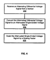
- a method comprises receiving an alternating differential voltage signal from a sensor.
- the differential voltage signal has an amplitude that changes over time.
- the alternating differential voltage signal is converted to an attenuated single-ended voltage signal that can be dynamically scaled.
- the attenuated single-ended voltage signal can be scaled by multiplying the attenuated single-ended voltage signal by a scaling factor.
- the scaling factor is selected relative to a signal-to-noise ratio of the scaled attenuated single-ended voltage signal.
- a system is described.
- the system is comprised of a sensor configured to produce an alternating differential voltage signal that has an Amplitude that changes over time. Further comprising the system is a first circuit that receives the alternating differential voltage signal and converts the alternating differential voltage signal to an attenuated single-ended voltage signal.
- a second circuit dynamically scales the attenuated single-ended voltage signal by multiplying the attenuated single-ended voltage signal by a scaling factor. The scaling factor is selected relative to a signal-to-noise ratio of the scaled attenuated single-ended voltage signal.
- embodiments of the invention described herein provide a magnetic sensor interface capable of adjusting signal conditioning dynamically such that the true positive and negative peaks of the input signal are maintained for a given target across its entire speed range (0-Max rpm), therefore increasing the signal to noise ratio at low speeds and avoiding clipping or distortion at high speeds.
- Magnetic sensor output voltages change drastically (e.g., 10mVp-p to 200Vp-p) with respect to the speed of a passing target. This characteristic poses a challenge when monitoring the sensor output of a target passing at a low speed with the same accuracy of the output when the target passes at high speed.
- Slow speed signals need gain to improve the signal to noise ratio while high speed signals must be attenuated to avoid clipping or distortion due to circuit limits.
- Embodiments described herein provide a way to monitor the performance/behavior of a given target across its entire speed range (0-Max rpm) with a magnetic sensor.
- Embodiments of this invention allow the capture of signal content from low amplitude signals that previously would have been difficult to separate from the noise.
- Embodiments also provide an opportunity for better signal to noise ratio across a wide range of target speeds and their corresponding signal amplitudes because of the dynamic scaling.
- the interface accepts a differential voltage from a magnetic sensor.
- the differential voltage is converted to a single ended voltage signal and attenuated (if necessary) to avoid signal clipping.
- the attenuated single-ended voltage signal is scaled (gained or attenuated) relative to a signal to noise ratio without clipping or altering the signal waveform.
- the attenuated single-ended voltage signal is scaled (gained or attenuated) to improve or maximize the signal to noise of the signal waveform.
- the gain or attenuation is selected by an algorithm within a digital processor or field programmable gate array (FPGA), which monitors the input signal continuously by means of an analog-to-digital converter (ADC).
- ADC provides a digital representation of the analog voltage seen across the magnetic sensor contacts.
- the ADC receives its input from the scaled attenuated single-ended voltage described herein. This provides a feedback loop that allows embodiments of the invention to detect the onset of clipping or signal alteration and adjust the scaling to ensure this does not happen.
- FIG. 1 illustrates an overview block diagram of one embodiment of the present invention.
- the sensor 102 detects a target 104 passing proximate to the sensor 102.
- the sensor 102 can be a passive magnetic or reluctance sensor, as known to one of ordinary skill in the art.
- the target 104 passes by the sensor 102, thus producing a voltage pulse or signal by the sensor 102.
- the sensor 102 moves past the target 104 and produces the voltage signal.
- the voltage signal produced by the sensor 102 is related to several factors including target 104 material, target 104 geometry or shape, gap size between the target 104 and sensor 102, and the speed at which the target 104 passes the sensor 102 (or the sensor 102 passes the target 104).
- the voltage signal is an alternating differential voltage pulse (i.e., not referenced to ground or any other common point).
- the voltage signal can be symmetrical or asymmetrical about a horizontal (zero) axis.
- the amplitude of the alternating voltage signal changes over time as the target 104 approaches, moves beneath and passes by the sensor 102 (or the sensor 102 approaches and moves past the target 104).
- the alternating voltage signal is a sine wave.
- the alternating voltage signal is not a sign wave.
- the sensor 102 is a passive magnetic sensor as available from one of many different manufacturers.
- the sensor 102 can be a passive magnetic sensor or variable reluctance sensor as available from Al-Tek Instruments, Inc.
- the sensor 102 can be an Al-Tel model number 70085-1010 passive magnetic sensor.
- the target 104 can be various devices.
- the target 104 can be the blade of a turbine, such as a steam turbine, a gas turbine, or the like.
- the target 104 can be the blade of a compressor, such as a compressor used in a gas turbine or the like.
- the target 104 can be a gear tooth.
- the alternating differential voltage signal produced by the sensor 102 is received by a circuit 106.
- the circuit 106 receives the alternating differential voltage signal and converts the alternating differential voltage signal to an attenuated single-ended voltage signal (i.e., referenced to ground or another common point).
- the circuit 106 attenuates or gains the alternating differential voltage signal depending upon the peak-to-peak value of the alternating differential voltage signal.
- the circuit 106 attenuates the alternating differential voltage by a fixed amount (i.e., the peak-to-peak value of the alternating differential voltage is constantly decreased by 10 percent, by 15 percent, by 20 percent, etc.).
- the circuit 106 converts the alternating differential voltage signal to the attenuated single-ended voltage signal by attenuating the alternating differential voltage signal by a fixed amount such that the attenuated single-ended voltage signal is less than or equal to a maximum attenuated voltage. In one aspect, the circuit 106 converts the alternating differential voltage signal to an attenuated single-ended voltage signal by multiplying the alternating differential voltage signal by a ratio of the maximum attenuated voltage to the maximum peak-to-peak value of the alternating differential voltage signal.
- the maximum peak-to-peak value of the alternating differential voltage signal can be about 250 volts peak-to-peak and the maximum attenuated voltage of the attenuated single-ended voltage signal can be about 30 volts peak-to-peak.
- the circuit 106 comprises a resistor divider 202 and an operational amplifier having a single-ended output 204 as shown in FIG. 2.
- FIG. 2 is a schematic diagram of an embodiment of a circuit 106 that can be used to convert the alternating differential voltage signal to an attenuated single-ended voltage signal according to one aspect of the present invention.
- converting the alternating differential voltage signal to an attenuated single-ended voltage signal comprises using the resistor divider 202 to divide the alternating differential voltage signal and providing a differential input to the operational amplifier having a single-ended output 204.
- the circuit of FIG. 2 is provided as a non-limiting example and it is to be appreciated that other circuits can be used to perform the same function.
- the attenuated single-ended voltage signal is dynamically scaled by multiplying the attenuated single-ended voltage signal by a scaling factor.
- the scaling factor is selected relative to a signal-to-noise ratio of the scaled attenuated single-ended voltage signal.
- the scaling factor is selected to improve or maximize the signal to noise of the signal waveform.
- the circuit 106 provides the attenuated single-ended voltage signal to a second circuit 108. The second circuit 108 dynamically scales the attenuated single-ended voltage signal.
- a field programmable gate array (FPGA) or digital processor 110 associated with the second circuit 108 automatically sets the scaling factor such that a product of the scaling factor times the attenuated single-ended voltage signal is less than or equal to a maximum input signal voltage.
- the maximum input signal voltage can be about 6.5 volts peak-to-peak.
- the FPGA or digital processor 110 associated with the second circuit 108 automatically sets the scaling factor in accordance with an algorithm.
- the algorithm comprises the FPGA or digital processor 110 receiving a digital input representative of the alternating differential voltage signal produced by the sensor 102 and scaling the attenuated single-ended voltage signal in proportion to that input.
- the digital input comprises the scaled output of the second circuit 108 converted to a digital signal by an analog-to-digital convertor (ADC) 112.
- ADC analog-to-digital convertor
- the digital input to the FPGA or digital processor 110 is below a lower defined value, Value L , then the scaling factor is greater than one and the attenuated single-ended voltage signal is amplified in order to increase its signal to noise ratio.
- the digital input to the FPGA or digital processor 110 is equal to or between a lower defined value, Value L , and an upper defined value, Value U , then the scaling factor is one and the attenuated single-ended voltage signal is neither amplified nor attenuated.
- an output 114 of circuit 108 can be provided to a monitoring system such as a turbine, compressor, or the like blade health monitoring system.
- the output 114 has a value that can be the same or less than the maximum input voltage level.
- operational characteristics and specifications of the monitoring system can determine the value for the maximum input voltage signal.
- operational characteristics and specifications of the ADC 112 can determine the value for the maximum input voltage signal.
- the second circuit 108 dynamically scaling the attenuated single-ended voltage signal using a scaling op-amp circuit 304 that has a digital potentiometer 302 controlled by the FPGA or digital processor 110.
- the FPGA or digital processor 110 provides an input to the digital potentiometer 302 that dynamically scales the attenuated single-ended voltage signal in accordance with the above-described algorithm.
- the FPGA or digital processor 110 scales the attenuated single-ended voltage signal by receiving a digital representation of the attenuated single-ended voltage signal from the ADC 112 and automatically adjusting the digital potentiometer 302 such that the scaling factor times the attenuated single-ended voltage level is less than or equal to the maximum input signal voltage.
- the scaling factor is 1 or greater such as, for example, 1.0. 1.1. 1.2. 2.0, 2.5, 10.0 etc. In another aspect the scaling factor is less than 1 such as for example, 0.95, 0.90, 0.5. 0.33, 0.10. 0.01, etc.
- FIG. 3 is a schematic diagram of an embodiment of a circuit 108 that can be used to dynamically scale the attenuated single-ended voltage signal according to one aspect of the present invention.
- dynamically scaling the attenuated single-ended voltage signal comprises the FPGA or processor 110 automatically adjusting the digital potentiometer 302 in accordance with the above-described algorithm such that an output of a scaling operational amplifier circuit 304 has an improved signal to noise ratio and is not so large as to result in clipping or distortion of the signal.
- the signal to noise ratio of the output is maximized.
- an output of the digital potentiometer 302 is used as an input to the scaling operational amplifier circuit 304 to provide dynamic scaling of the output of the scaling operational amplifier circuit 304.
- digital potentiometer 302 can be further comprised of capacitor C124 having a value of 1 micro-farad.
- the digital potentiometer 302 can be a single-channel, 1024-position digital potentiometer as available from, for example, Analog Devices, Inc.
- the digital potentiometer 302 can be an Analog Devices, Inc. model AD5293 digital potentiometer. While the circuit of FIG. 3 is provided as a non-limiting example, it is to be appreciated that other circuits can be used to perform the same function.
- an alternating differential voltage signal is received from a sensor.
- the sensor is a passive magnetic sensor.
- the sensor is a variable reluctance sensor.
- the alternating differential voltage signal has an amplitude that changes over time. For example, if the sensor were monitoring a stage of blades of a turbine, then the amplitude of the alternating differential voltage signal from the sensor would increase as the machine ramps up from zero revolutions per minute (rpm) to operating speed (e.g., 3600 rpm).
- the alternating differential voltage signal produced by the sensor is related to a target's material composition, a gap between the sensor and the target, and a speed at which the target passes the sensor (or sensor passes the target).
- the target is a turbine blade.
- the alternating differential voltage signal is converted to an attenuated single-ended voltage signal.
- the alternating differential voltage signal has a maximum peak-to-peak value and converting the alternating differential voltage signal to an attenuated single-ended voltage signal comprises the alternating differential voltage signal multiplied by a ratio of a maximum attenuated voltage to the maximum peak-to-peak value.
- the maximum peak-to-peak value of the alternating differential voltage signal can be about 250 volts peak-to-peak and the maximum attenuated voltage of the attenuated single-ended voltage signal can be about 30 volts peak-to-peak.
- converting the alternating differential voltage signal to the attenuated single-ended voltage signal comprises attenuation of the alternating differential voltage signal by a fixed amount such that the attenuated single-ended voltage signal is less than or equal to the maximum attenuated voltage.
- converting the alternating differential voltage signal to an attenuated single-ended voltage signal comprises using a resistor divider to divide the alternating differential voltage signal and providing a differential input to an operational amplifier having a single-ended output.
- the single-ended voltage signal is dynamically scaled by multiplying the attenuated single-ended voltage signal by a scaling factor.
- the scaling factor is selected to maximize a signal-to-noise ratio of the scaled attenuated single-ended voltage signal.
- dynamically scaling the attenuated single-ended voltage signal by multiplying the attenuated single-ended voltage signal by a scaling factor comprises selecting the scaling factor such that a product of the scaling factor times the attenuated single-ended voltage signal is less than or equal to a maximum input signal voltage, as described herein.
- the maximum input signal voltage can be about 6.5 volts peak-to-peak.
- dynamically scaling the attenuated single-ended voltage signal by multiplying the attenuated single-ended voltage level by the scaling factor comprises dynamically scaling the attenuated single-ended voltage signal using a scaling op-amp circuit that has a digital potentiometer controlled by an field programmable gate array (FPGA) or digital processor.
- the FPGA or digital processor dynamically scales the attenuated single-ended voltage signal by receiving a digital representation of the attenuated single-ended voltage signal and adjusts the digital potentiometer such that the scaling factor times the attenuated single-ended voltage level is less than or equal to the maximum input signal voltage.
- the scaling factor is 1 or greater such as, for example, 1.0. 1.1. 1.2. 2.0, 2.5, 10.0 etc. In another aspect the scaling factor is less than 1 such as for example, 0.95, 0.90, 0.5. 0.33, 0.10. 0.01, etc.
- a unit such as the FPGA or processor 110 can be software, hardware, or a combination of software and hardware.
- the units can comprise the digital potentiometer control software 506 as illustrated in FIG. 5 and described below.
- the units can comprise a computer 501 as illustrated in FIG. 5 and described below.
- the processor 503 of the computer 501 can be used to execute the algorithm described above as embodied in computer-executable code and to control the digital potentiometer 302 as described herein.
- FIG. 5 is a block diagram illustrating an exemplary operating environment for performing the disclosed methods.
- This exemplary operating environment is only an example of an operating environment and is not intended to suggest any limitation as to the scope of use or functionality of operating environment architecture. Neither should the operating environment be interpreted as having any dependency or requirement relating to any one or combination of components illustrated in the exemplary operating environment.
- the present methods and systems can be operational with numerous other general purpose or special purpose computing system environments or configurations.
- Examples of well known computing systems, environments, and/or configurations that can be suitable for use with the systems and methods comprise, but are not limited to, embedded processing units, personal computers, server computers, laptop devices, and multiprocessor systems. Additional examples comprise machine monitoring systems, programmable consumer electronics, network PCs, minicomputers, mainframe computers, smart meters, smart-grid components, distributed computing environments that comprise any of the above systems or devices, FPGA's, and the like.
- the processing of the disclosed methods and systems can be performed by software components.
- the disclosed systems and methods can be described in the general context of computer-executable instructions, such as program modules, being executed by one or more computers or other devices.
- program modules comprise computer code, routines, programs, objects, components, data structures, etc. that perform particular tasks or implement particular abstract data types.
- the disclosed methods can also be practiced in grid-based and distributed computing environments where tasks are performed by remote processing devices that are linked through a communications network.
- program modules can be located in both local and remote computer storage media including memory storage devices.
- the components of the computer 501 can comprise, but are not limited to, one or more processors or processing units 503, a system memory 512, and a system bus 513 that couples various system components including the processor 503 to the system memory 512.
- processors or processing units 503 the system can utilize parallel computing.
- the system bus 513 represents one or more of several possible types of bus structures, including a memory bus or memory controller, a peripheral bus, an accelerated graphics port, and a processor or local bus using any of a variety of bus architectures.
- bus architectures can comprise an Industry Standard Architecture (ISA) bus, a Micro Channel Architecture (MCA) bus, an Enhanced ISA (EISA) bus, a Video Electronics Standards Association (VESA) local bus, an Accelerated Graphics Port (AGP) bus, and a Peripheral Component Interconnects (PCI), a PCI-Express bus, a Personal Computer Memory Card Industry Association (PCMCIA), Universal Serial Bus (USB) and the like.
- ISA Industry Standard Architecture
- MCA Micro Channel Architecture
- EISA Enhanced ISA
- VESA Video Electronics Standards Association
- AGP Accelerated Graphics Port
- PCI Peripheral Component Interconnects
- PCI-Express PCI-Express
- PCMCIA Personal Computer Memory Card Industry Association
- USB Universal Serial Bus
- the bus 513, and all buses specified in this description can also be implemented over a wired or wireless network connection and each of the subsystems, including the processor 503, a mass storage device 504, an operating system 505, digital potentiometer control software 306, control algorithm data 307 (e.g., the values for Value L and Value U , gain or attenuation settings, etc.), a network adapter 508, system memory 512, an Input/Output Interface 510, a display adapter 509, a display device 511, and a human machine interface 502, can be contained within one or more remote computing devices or clients 514a,b,c at physically separate locations, connected through buses of this form, in effect implementing a fully distributed system or distributed architecture.
- the computer 501 typically comprises a variety of computer readable media. Exemplary readable media can be any available media that is non-transitory and accessible by the computer 501 and comprises, for example and not meant to be limiting, both volatile and non-volatile media, removable and non-removable media.
- the system memory 512 comprises computer readable media in the form of volatile memory, such as random access memory (RAM), and/or non-volatile memory, such as read only memory (ROM).
- RAM random access memory
- ROM read only memory
- the system memory 512 typically contains data such as control algorithm data 507 and/or program modules such as operating system 505 and digital potentiometer control software 506 that are immediately accessible to and/or are presently operated on by the processing unit 503.
- the computer 501 can also comprise other non-transitory, removable/non-removable, volatile/non-volatile computer storage media.
- FIG. 5 illustrates a mass storage device 504 that can provide non-volatile storage of computer code, computer readable instructions, data structures, program modules, and other data for the computer 501.
- a mass storage device 504 can be a hard disk, a removable magnetic disk, a removable optical disk, magnetic cassettes or other magnetic storage devices, flash memory cards, CD-ROM, digital versatile disks (DVD) or other optical storage, random access memories (RAM), read only memories (ROM), electrically erasable programmable read-only memory (EEPROM), and the like.
- any number of program modules can be stored on the mass storage device 504, including by way of example, an operating system 505 and digital potentiometer control software 506.
- Each of the operating system 505 and correlation software 506 (or some combination thereof) can comprise elements of the programming and the digital potentiometer control software 506.
- Control algorithm data 507 can also be stored on the mass storage device 504.
- Control algorithm data 507 can be stored in any of one or more databases known in the art. Examples of such databases comprise, DB2®, Microsoft® Access, Microsoft® SQL Server, Oracle®, mySQL, PostgreSQL, and the like. The databases can be centralized or distributed across multiple systems.
- the user can enter commands and information into the computer 501 via an input device (not shown).
- input devices comprise, but are not limited to, a keyboard, pointing device (e.g., a "mouse"), a microphone, a joystick, a scanner, tactile input devices such as gloves, and other body coverings, and the like
- a human machine interface 502 that is coupled to the system bus 513, but can be connected by other interface and bus structures, such as a parallel port, game port, an IEEE 1394 Port (also known as a Firewire port), a serial port, or a universal serial bus (USB).
- a display device 511 can also be connected to the system bus 513 via an interface, such as a display adapter 509. It is contemplated that the computer 501 can have more than one display adapter 509 and the computer 501 can have more than one display device 511.
- a display device can be a monitor, an LCD (Liquid Crystal Display), or a projector.
- other output peripheral devices can comprise components such as speakers (not shown) and a printer (not shown), which can be connected to the computer 501 via Input/Output Interface 510. Any step and/or result of the methods can be output in any form to an output device. Such output can be any form of visual representation, including, but not limited to, textual, graphical, animation, audio, tactile, and the like.
- the computer 501 can operate in a networked environment using logical connections to one or more remote computing devices or clients 514a,b,c.
- a remote computing device 514 can be a personal computer, portable computer, a server, a router, a network computer, a smart meter, a vendor or manufacture's computing device, smart grid components, a peer device or other common network node, and so on.
- Logical connections between the computer 501 and a remote computing device or client 514a,b,c can be made via a local area network (LAN) and a general wide area network (WAN).
- LAN local area network
- WAN wide area network
- a network adapter 508 can be implemented in both wired and wireless environments. Such networking environments are conventional and commonplace in offices, enterprise-wide computer networks, intranets, and other networks 515 such as the Internet.
- Computer readable media can comprise “computer storage media” and “communications media.”
- “Computer storage media” comprise volatile and non-volatile, removable and non-removable media implemented in any methods or technology for storage of information such as computer readable instructions, data structures, program modules, or other data.
- Exemplary computer storage media comprises, but is not limited to, RAM, ROM, EEPROM, flash memory or other memory technology, CD-ROM, digital versatile disks (DVD) or other optical storage, magnetic cassettes, magnetic tape, magnetic disk storage or other magnetic storage devices, or any other medium which can be used to store the desired information and which can be accessed by a computer.
- the methods and systems can employ Artificial Intelligence techniques such as machine learning and iterative learning.
- Artificial Intelligence techniques such as machine learning and iterative learning. Examples of such techniques include, but are not limited to, expert systems, case based reasoning, Bayesian networks, behavior based AI, neural networks, fuzzy systems, evolutionary computation (e.g. genetic algorithms), swarm intelligence (e.g. ant algorithms), and hybrid intelligent systems (e.g. Expert inference rules generated through a neural network or production rules from statistical learning).
- an embodiment of the present invention can be used in a turbine blade monitoring system, though other uses are contemplated within the scope of the invention.
- sensors 102 as described herein can be used to detect changes in the time of arrival (TOA) of turbine blades in a stage of a gas turbine. Changes in the TOA can be an indication of blade failure.
- TOA time of arrival
- the basic principle of blade-pass measurement involves establishing a time reference using a once-per-turn (keyphasor) transducer, then, for each blade in a row, measuring the time of arrival (TOA) of the blade as it moves past a blade pass detection transducer. Dynamic and static changes in TOA are analyzed to detect shifts in blade resonance frequencies and/or static lean that may indicate the presence of a crack.
- sensors go through a range of voltages as the machine ramps from zero to full speed (blade tip speeds can exceed the speed of sound at full machine speed)
- the sensor outputs need to be scaled (i.e. amplified or attenuated) during the ramp-up process in order to improve signal to noise ratio at lower voltages and to avoid clipping at distortion at high voltage levels. This allows the sensor outputs to be used to perform TOA calculations in order to monitor turbine blade health. Therefore, embodiments of the systems and methods described herein can be used to meet those requirements.
- embodiments of the present invention may be configured as a system, method, or computer program product. Accordingly, embodiments of the present invention may be comprised of various means including entirely of hardware, entirely of software, or any combination of software and hardware. Furthermore, embodiments of the present invention may take the form of a computer program product on a computer-readable storage medium having computer-readable program instructions (e.g., computer software) embodied in the storage medium. Any suitable non-transitory computer-readable storage medium may be utilized including hard disks, CD-ROMs, optical storage devices, or magnetic storage devices.
- Embodiments of the present invention have been described above with reference to block diagrams and flowchart illustrations of methods, apparatuses (i.e., systems) and computer program products. It will be understood that each block of the block diagrams and flowchart illustrations, and combinations of blocks in the block diagrams and flowchart illustrations, respectively, can be implemented by various means including computer program instructions. These computer program instructions may be loaded onto a general purpose computer, special purpose computer, or other programmable data processing apparatus, such as the one or more processors 503 discussed above with reference to FIG. 5 , to produce a machine, such that the instructions which execute on the computer or other programmable data processing apparatus create a means for implementing the functions specified in the flowchart block or blocks.
- These computer program instructions may also be stored in a non-transitory computer-readable memory that can direct a computer or other programmable data processing apparatus (e.g., one or more processors 503 of FIG. 5 ) to function in a particular manner, such that the instructions stored in the computer-readable memory produce an article of manufacture including computer-readable instructions for implementing the function specified in the flowchart block or blocks.
- the computer program instructions may also be loaded onto a computer or other programmable data processing apparatus to cause a series of operational steps to be performed on the computer or other programmable apparatus to produce a computer-implemented process such that the instructions that execute on the computer or other programmable apparatus provide steps for implementing the functions specified in the flowchart block or blocks.
- blocks of the block diagrams and flowchart illustrations support combinations of means for performing the specified functions, combinations of steps for performing the specified functions and program instruction means for performing the specified functions. It will also be understood that each block of the block diagrams and flowchart illustrations, and combinations of blocks in the block diagrams and flowchart illustrations, can be implemented by special purpose hardware-based computer systems that perform the specified functions or steps, or combinations of special purpose hardware and computer instructions.
Landscapes
- Physics & Mathematics (AREA)
- General Physics & Mathematics (AREA)
- Transmission And Conversion Of Sensor Element Output (AREA)
- Measuring Magnetic Variables (AREA)
- Measurement Of Length, Angles, Or The Like Using Electric Or Magnetic Means (AREA)
Applications Claiming Priority (1)
| Application Number | Priority Date | Filing Date | Title |
|---|---|---|---|
| US13/033,249 US8710825B2 (en) | 2011-02-23 | 2011-02-23 | Method and system of a sensor interface having dynamic automatic gain control |
Publications (2)
| Publication Number | Publication Date |
|---|---|
| EP2492695A1 EP2492695A1 (en) | 2012-08-29 |
| EP2492695B1 true EP2492695B1 (en) | 2013-12-04 |
Family
ID=45656261
Family Applications (1)
| Application Number | Title | Priority Date | Filing Date |
|---|---|---|---|
| EP12156301.9A Active EP2492695B1 (en) | 2011-02-23 | 2012-02-21 | Method and system of a sensor interface having dynamic automatic gain control |
Country Status (7)
| Country | Link |
|---|---|
| US (1) | US8710825B2 (enExample) |
| EP (1) | EP2492695B1 (enExample) |
| JP (1) | JP2012211581A (enExample) |
| CN (1) | CN102739193A (enExample) |
| AU (1) | AU2012200975B2 (enExample) |
| CA (1) | CA2768566C (enExample) |
| IN (1) | IN2012DE00446A (enExample) |
Families Citing this family (7)
| Publication number | Priority date | Publication date | Assignee | Title |
|---|---|---|---|---|
| US9407131B2 (en) * | 2012-04-17 | 2016-08-02 | Bwxt Nuclear Operations Group, Inc. | Positional encoder and control rod position indicator for nuclear reactor using same |
| JP6166904B2 (ja) * | 2013-01-25 | 2017-07-19 | テルモ株式会社 | 血糖計 |
| US8963615B1 (en) | 2013-01-31 | 2015-02-24 | General Electric Company | Automatic bipolar signal switching |
| US9657588B2 (en) | 2013-12-26 | 2017-05-23 | General Electric Company | Methods and systems to monitor health of rotor blades |
| CN108169531B (zh) * | 2017-12-28 | 2023-09-26 | 广东机电职业技术学院 | 一种新型衰减网络电路 |
| FI128771B (en) * | 2019-04-02 | 2020-11-30 | Aito Bv | Piezoelectric user interface arrangement and method for using piezoelectric units in user interface arrangement |
| CN112445260B (zh) * | 2020-11-25 | 2022-09-30 | 上海城建职业学院 | 一种零点漂移自动调节系统和方法 |
Family Cites Families (9)
| Publication number | Priority date | Publication date | Assignee | Title |
|---|---|---|---|---|
| GB1090143A (en) | 1965-04-07 | 1967-11-08 | Hawker Siddeley Dynamics Ltd | Improvements in or relating to electrical control systems for engines |
| CA1258930A (en) * | 1986-12-24 | 1989-08-29 | Reinhard Rosch | Active impedance line feed circuit |
| US5510706A (en) | 1994-02-22 | 1996-04-23 | Delco Electronics Corporation | Differential to single-ended conversion circuit for a magnetic wheel speed sensor |
| US5477142A (en) | 1994-02-22 | 1995-12-19 | Delco Electronics Corporation | Variable reluctance sensor interface using a differential input and digital adaptive control |
| US6040692A (en) | 1998-05-18 | 2000-03-21 | Delco Electronics Corporaiton | Variable attenuation circuit for a differential variable reluctance sensor using current mode |
| US6133728A (en) | 1998-05-18 | 2000-10-17 | Delco Electronics Corporation | Current mode differential to single-ended conversion circuit for a magnetic wheel speed sensor |
| US6674279B2 (en) | 2002-05-09 | 2004-01-06 | Delphi Technologies, Inc. | Variable attenuation circuit for a differential variable reluctance sensor with enhanced initial threshold accuracy |
| US7498886B2 (en) | 2006-01-27 | 2009-03-03 | Via Technologies, Inc. | Clock distribution system and method thereof |
| US8346100B2 (en) | 2009-10-12 | 2013-01-01 | Avago Technologies Fiber Ip (Singapore) Pte. Ltd | Apparatus and method for monitoring received optical power in an optical receiver over a wide range of received power with high accuracy |
-
2011
- 2011-02-23 US US13/033,249 patent/US8710825B2/en active Active
-
2012
- 2012-02-16 CA CA2768566A patent/CA2768566C/en active Active
- 2012-02-16 IN IN446DE2012 patent/IN2012DE00446A/en unknown
- 2012-02-20 AU AU2012200975A patent/AU2012200975B2/en active Active
- 2012-02-20 JP JP2012033479A patent/JP2012211581A/ja active Pending
- 2012-02-21 EP EP12156301.9A patent/EP2492695B1/en active Active
- 2012-02-23 CN CN2012100536306A patent/CN102739193A/zh active Pending
Also Published As
| Publication number | Publication date |
|---|---|
| AU2012200975A1 (en) | 2012-09-06 |
| CN102739193A (zh) | 2012-10-17 |
| CA2768566A1 (en) | 2012-08-23 |
| EP2492695A1 (en) | 2012-08-29 |
| JP2012211581A (ja) | 2012-11-01 |
| US20120212214A1 (en) | 2012-08-23 |
| AU2012200975B2 (en) | 2015-06-18 |
| US8710825B2 (en) | 2014-04-29 |
| CA2768566C (en) | 2018-06-05 |
| IN2012DE00446A (enExample) | 2015-06-05 |
Similar Documents
| Publication | Publication Date | Title |
|---|---|---|
| EP2492695B1 (en) | Method and system of a sensor interface having dynamic automatic gain control | |
| EP2492694B1 (en) | Method and system of a sensor interface having dynamic automatic gain control dependent on speed | |
| US9645046B2 (en) | Fault detection system and associated method | |
| CN112629647A (zh) | 大跨悬索桥涡振事件的实时识别和监测预警方法 | |
| CN103376291A (zh) | 异常检查方法及异常检查装置 | |
| CN107588947B (zh) | 考虑运行工况和信息简化的风电机组传动链状态监测方法 | |
| EP2461222B1 (en) | Method and system for detection of machine operation state for monitoring purposes | |
| GB2455798A (en) | Monitoring a rotating shaft in a gas turbine | |
| US10895873B2 (en) | Machine health monitoring of rotating machinery | |
| EP2073022B1 (en) | Method and apparatus for monitoring the rotational speed of a gas turbine shaft | |
| CN112697438B (zh) | 基于音轮的涡桨发动机桨距-相角-转速测量装置及方法 | |
| JP2015102402A (ja) | タービンブレード振動変位評価方法及び装置 | |
| US11592455B2 (en) | Adaptive voltage threshold for turbine engine | |
| CN109084891A (zh) | 一种基于受力变化的旋转体噪声测试系统及测试方法 | |
| EP4231020A1 (en) | Sensing systems | |
| WO2024258963A1 (en) | Integrated machine speed signal waveform capture | |
| CN106771322A (zh) | 一种磁电式转速传感器信号畸变的处理方法 | |
| CN121521988A (zh) | 一种基于周期性载荷同步的金属结构件裂纹监测方法 | |
| CN121752906A (zh) | 集成式机器速度信号波形捕获 | |
| WO2023132235A1 (ja) | 振動監視装置、過給機、及び振動監視方法 | |
| CN121278565A (zh) | 一种工业机器人减速器健康状态的评估方法 | |
| CN121164729A (zh) | 测功机的防电磁干扰测试方法及相关设备 | |
| JPH03221867A (ja) | 回転検出装置 | |
| Kirana | The Design of Tachometer Contact and Non-Contact Using Microcontroller |
Legal Events
| Date | Code | Title | Description |
|---|---|---|---|
| PUAI | Public reference made under article 153(3) epc to a published international application that has entered the european phase |
Free format text: ORIGINAL CODE: 0009012 |
|
| AK | Designated contracting states |
Kind code of ref document: A1 Designated state(s): AL AT BE BG CH CY CZ DE DK EE ES FI FR GB GR HR HU IE IS IT LI LT LU LV MC MK MT NL NO PL PT RO RS SE SI SK SM TR |
|
| AX | Request for extension of the european patent |
Extension state: BA ME |
|
| 17P | Request for examination filed |
Effective date: 20130228 |
|
| GRAP | Despatch of communication of intention to grant a patent |
Free format text: ORIGINAL CODE: EPIDOSNIGR1 |
|
| RIC1 | Information provided on ipc code assigned before grant |
Ipc: G01P 3/46 20060101AFI20130702BHEP Ipc: G01P 3/488 20060101ALI20130702BHEP Ipc: G01P 3/487 20060101ALI20130702BHEP |
|
| INTG | Intention to grant announced |
Effective date: 20130719 |
|
| GRAS | Grant fee paid |
Free format text: ORIGINAL CODE: EPIDOSNIGR3 |
|
| GRAA | (expected) grant |
Free format text: ORIGINAL CODE: 0009210 |
|
| AK | Designated contracting states |
Kind code of ref document: B1 Designated state(s): AL AT BE BG CH CY CZ DE DK EE ES FI FR GB GR HR HU IE IS IT LI LT LU LV MC MK MT NL NO PL PT RO RS SE SI SK SM TR |
|
| REG | Reference to a national code |
Ref country code: GB Ref legal event code: FG4D |
|
| REG | Reference to a national code |
Ref country code: CH Ref legal event code: EP |
|
| REG | Reference to a national code |
Ref country code: IE Ref legal event code: FG4D Ref country code: AT Ref legal event code: REF Ref document number: 643742 Country of ref document: AT Kind code of ref document: T Effective date: 20140115 |
|
| REG | Reference to a national code |
Ref country code: DE Ref legal event code: R096 Ref document number: 602012000589 Country of ref document: DE Effective date: 20140130 |
|
| REG | Reference to a national code |
Ref country code: NL Ref legal event code: VDEP Effective date: 20131204 |
|
| REG | Reference to a national code |
Ref country code: AT Ref legal event code: MK05 Ref document number: 643742 Country of ref document: AT Kind code of ref document: T Effective date: 20131204 |
|
| PG25 | Lapsed in a contracting state [announced via postgrant information from national office to epo] |
Ref country code: NO Free format text: LAPSE BECAUSE OF FAILURE TO SUBMIT A TRANSLATION OF THE DESCRIPTION OR TO PAY THE FEE WITHIN THE PRESCRIBED TIME-LIMIT Effective date: 20140304 Ref country code: FI Free format text: LAPSE BECAUSE OF FAILURE TO SUBMIT A TRANSLATION OF THE DESCRIPTION OR TO PAY THE FEE WITHIN THE PRESCRIBED TIME-LIMIT Effective date: 20131204 Ref country code: SE Free format text: LAPSE BECAUSE OF FAILURE TO SUBMIT A TRANSLATION OF THE DESCRIPTION OR TO PAY THE FEE WITHIN THE PRESCRIBED TIME-LIMIT Effective date: 20131204 Ref country code: LT Free format text: LAPSE BECAUSE OF FAILURE TO SUBMIT A TRANSLATION OF THE DESCRIPTION OR TO PAY THE FEE WITHIN THE PRESCRIBED TIME-LIMIT Effective date: 20131204 Ref country code: HR Free format text: LAPSE BECAUSE OF FAILURE TO SUBMIT A TRANSLATION OF THE DESCRIPTION OR TO PAY THE FEE WITHIN THE PRESCRIBED TIME-LIMIT Effective date: 20131204 Ref country code: NL Free format text: LAPSE BECAUSE OF FAILURE TO SUBMIT A TRANSLATION OF THE DESCRIPTION OR TO PAY THE FEE WITHIN THE PRESCRIBED TIME-LIMIT Effective date: 20131204 |
|
| REG | Reference to a national code |
Ref country code: LT Ref legal event code: MG4D |
|
| PG25 | Lapsed in a contracting state [announced via postgrant information from national office to epo] |
Ref country code: AT Free format text: LAPSE BECAUSE OF FAILURE TO SUBMIT A TRANSLATION OF THE DESCRIPTION OR TO PAY THE FEE WITHIN THE PRESCRIBED TIME-LIMIT Effective date: 20131204 Ref country code: RS Free format text: LAPSE BECAUSE OF FAILURE TO SUBMIT A TRANSLATION OF THE DESCRIPTION OR TO PAY THE FEE WITHIN THE PRESCRIBED TIME-LIMIT Effective date: 20131204 Ref country code: LV Free format text: LAPSE BECAUSE OF FAILURE TO SUBMIT A TRANSLATION OF THE DESCRIPTION OR TO PAY THE FEE WITHIN THE PRESCRIBED TIME-LIMIT Effective date: 20131204 Ref country code: CY Free format text: LAPSE BECAUSE OF FAILURE TO SUBMIT A TRANSLATION OF THE DESCRIPTION OR TO PAY THE FEE WITHIN THE PRESCRIBED TIME-LIMIT Effective date: 20131204 |
|
| PG25 | Lapsed in a contracting state [announced via postgrant information from national office to epo] |
Ref country code: EE Free format text: LAPSE BECAUSE OF FAILURE TO SUBMIT A TRANSLATION OF THE DESCRIPTION OR TO PAY THE FEE WITHIN THE PRESCRIBED TIME-LIMIT Effective date: 20131204 Ref country code: BE Free format text: LAPSE BECAUSE OF FAILURE TO SUBMIT A TRANSLATION OF THE DESCRIPTION OR TO PAY THE FEE WITHIN THE PRESCRIBED TIME-LIMIT Effective date: 20131204 Ref country code: IS Free format text: LAPSE BECAUSE OF FAILURE TO SUBMIT A TRANSLATION OF THE DESCRIPTION OR TO PAY THE FEE WITHIN THE PRESCRIBED TIME-LIMIT Effective date: 20140404 |
|
| PG25 | Lapsed in a contracting state [announced via postgrant information from national office to epo] |
Ref country code: PT Free format text: LAPSE BECAUSE OF FAILURE TO SUBMIT A TRANSLATION OF THE DESCRIPTION OR TO PAY THE FEE WITHIN THE PRESCRIBED TIME-LIMIT Effective date: 20140404 Ref country code: ES Free format text: LAPSE BECAUSE OF FAILURE TO SUBMIT A TRANSLATION OF THE DESCRIPTION OR TO PAY THE FEE WITHIN THE PRESCRIBED TIME-LIMIT Effective date: 20131204 Ref country code: RO Free format text: LAPSE BECAUSE OF FAILURE TO SUBMIT A TRANSLATION OF THE DESCRIPTION OR TO PAY THE FEE WITHIN THE PRESCRIBED TIME-LIMIT Effective date: 20131204 Ref country code: PL Free format text: LAPSE BECAUSE OF FAILURE TO SUBMIT A TRANSLATION OF THE DESCRIPTION OR TO PAY THE FEE WITHIN THE PRESCRIBED TIME-LIMIT Effective date: 20131204 Ref country code: SK Free format text: LAPSE BECAUSE OF FAILURE TO SUBMIT A TRANSLATION OF THE DESCRIPTION OR TO PAY THE FEE WITHIN THE PRESCRIBED TIME-LIMIT Effective date: 20131204 Ref country code: CZ Free format text: LAPSE BECAUSE OF FAILURE TO SUBMIT A TRANSLATION OF THE DESCRIPTION OR TO PAY THE FEE WITHIN THE PRESCRIBED TIME-LIMIT Effective date: 20131204 |
|
| REG | Reference to a national code |
Ref country code: DE Ref legal event code: R097 Ref document number: 602012000589 Country of ref document: DE |
|
| PG25 | Lapsed in a contracting state [announced via postgrant information from national office to epo] |
Ref country code: MC Free format text: LAPSE BECAUSE OF FAILURE TO SUBMIT A TRANSLATION OF THE DESCRIPTION OR TO PAY THE FEE WITHIN THE PRESCRIBED TIME-LIMIT Effective date: 20131204 Ref country code: LU Free format text: LAPSE BECAUSE OF FAILURE TO SUBMIT A TRANSLATION OF THE DESCRIPTION OR TO PAY THE FEE WITHIN THE PRESCRIBED TIME-LIMIT Effective date: 20140221 |
|
| PLBE | No opposition filed within time limit |
Free format text: ORIGINAL CODE: 0009261 |
|
| STAA | Information on the status of an ep patent application or granted ep patent |
Free format text: STATUS: NO OPPOSITION FILED WITHIN TIME LIMIT |
|
| PG25 | Lapsed in a contracting state [announced via postgrant information from national office to epo] |
Ref country code: DK Free format text: LAPSE BECAUSE OF FAILURE TO SUBMIT A TRANSLATION OF THE DESCRIPTION OR TO PAY THE FEE WITHIN THE PRESCRIBED TIME-LIMIT Effective date: 20131204 |
|
| 26N | No opposition filed |
Effective date: 20140905 |
|
| REG | Reference to a national code |
Ref country code: FR Ref legal event code: ST Effective date: 20141031 |
|
| REG | Reference to a national code |
Ref country code: IE Ref legal event code: MM4A |
|
| REG | Reference to a national code |
Ref country code: DE Ref legal event code: R097 Ref document number: 602012000589 Country of ref document: DE Effective date: 20140905 |
|
| PG25 | Lapsed in a contracting state [announced via postgrant information from national office to epo] |
Ref country code: FR Free format text: LAPSE BECAUSE OF NON-PAYMENT OF DUE FEES Effective date: 20140228 Ref country code: IE Free format text: LAPSE BECAUSE OF NON-PAYMENT OF DUE FEES Effective date: 20140221 |
|
| PG25 | Lapsed in a contracting state [announced via postgrant information from national office to epo] |
Ref country code: SI Free format text: LAPSE BECAUSE OF FAILURE TO SUBMIT A TRANSLATION OF THE DESCRIPTION OR TO PAY THE FEE WITHIN THE PRESCRIBED TIME-LIMIT Effective date: 20131204 |
|
| PG25 | Lapsed in a contracting state [announced via postgrant information from national office to epo] |
Ref country code: IT Free format text: LAPSE BECAUSE OF FAILURE TO SUBMIT A TRANSLATION OF THE DESCRIPTION OR TO PAY THE FEE WITHIN THE PRESCRIBED TIME-LIMIT Effective date: 20131204 |
|
| REG | Reference to a national code |
Ref country code: CH Ref legal event code: PL |
|
| PG25 | Lapsed in a contracting state [announced via postgrant information from national office to epo] |
Ref country code: LI Free format text: LAPSE BECAUSE OF NON-PAYMENT OF DUE FEES Effective date: 20150228 Ref country code: CH Free format text: LAPSE BECAUSE OF NON-PAYMENT OF DUE FEES Effective date: 20150228 |
|
| PG25 | Lapsed in a contracting state [announced via postgrant information from national office to epo] |
Ref country code: MT Free format text: LAPSE BECAUSE OF FAILURE TO SUBMIT A TRANSLATION OF THE DESCRIPTION OR TO PAY THE FEE WITHIN THE PRESCRIBED TIME-LIMIT Effective date: 20131204 |
|
| PG25 | Lapsed in a contracting state [announced via postgrant information from national office to epo] |
Ref country code: SM Free format text: LAPSE BECAUSE OF FAILURE TO SUBMIT A TRANSLATION OF THE DESCRIPTION OR TO PAY THE FEE WITHIN THE PRESCRIBED TIME-LIMIT Effective date: 20131204 |
|
| PG25 | Lapsed in a contracting state [announced via postgrant information from national office to epo] |
Ref country code: BG Free format text: LAPSE BECAUSE OF FAILURE TO SUBMIT A TRANSLATION OF THE DESCRIPTION OR TO PAY THE FEE WITHIN THE PRESCRIBED TIME-LIMIT Effective date: 20131204 Ref country code: GR Free format text: LAPSE BECAUSE OF FAILURE TO SUBMIT A TRANSLATION OF THE DESCRIPTION OR TO PAY THE FEE WITHIN THE PRESCRIBED TIME-LIMIT Effective date: 20140305 |
|
| PG25 | Lapsed in a contracting state [announced via postgrant information from national office to epo] |
Ref country code: TR Free format text: LAPSE BECAUSE OF FAILURE TO SUBMIT A TRANSLATION OF THE DESCRIPTION OR TO PAY THE FEE WITHIN THE PRESCRIBED TIME-LIMIT Effective date: 20131204 Ref country code: HU Free format text: LAPSE BECAUSE OF FAILURE TO SUBMIT A TRANSLATION OF THE DESCRIPTION OR TO PAY THE FEE WITHIN THE PRESCRIBED TIME-LIMIT; INVALID AB INITIO Effective date: 20120221 |
|
| PG25 | Lapsed in a contracting state [announced via postgrant information from national office to epo] |
Ref country code: MK Free format text: LAPSE BECAUSE OF FAILURE TO SUBMIT A TRANSLATION OF THE DESCRIPTION OR TO PAY THE FEE WITHIN THE PRESCRIBED TIME-LIMIT Effective date: 20131204 |
|
| PG25 | Lapsed in a contracting state [announced via postgrant information from national office to epo] |
Ref country code: AL Free format text: LAPSE BECAUSE OF FAILURE TO SUBMIT A TRANSLATION OF THE DESCRIPTION OR TO PAY THE FEE WITHIN THE PRESCRIBED TIME-LIMIT Effective date: 20131204 |
|
| PGFP | Annual fee paid to national office [announced via postgrant information from national office to epo] |
Ref country code: DE Payment date: 20250321 Year of fee payment: 14 |
|
| PGFP | Annual fee paid to national office [announced via postgrant information from national office to epo] |
Ref country code: GB Payment date: 20250325 Year of fee payment: 14 |