EP2491409B1 - Testen kapazitiver öffnungen in umgebungen mit schwachen signalen - Google Patents
Testen kapazitiver öffnungen in umgebungen mit schwachen signalen Download PDFInfo
- Publication number
- EP2491409B1 EP2491409B1 EP10843363.2A EP10843363A EP2491409B1 EP 2491409 B1 EP2491409 B1 EP 2491409B1 EP 10843363 A EP10843363 A EP 10843363A EP 2491409 B1 EP2491409 B1 EP 2491409B1
- Authority
- EP
- European Patent Office
- Prior art keywords
- probe
- component
- probe assembly
- pins
- assembly
- Prior art date
- Legal status (The legal status is an assumption and is not a legal conclusion. Google has not performed a legal analysis and makes no representation as to the accuracy of the status listed.)
- Active
Links
Images


Classifications
-
- G—PHYSICS
- G01—MEASURING; TESTING
- G01R—MEASURING ELECTRIC VARIABLES; MEASURING MAGNETIC VARIABLES
- G01R31/00—Arrangements for testing electric properties; Arrangements for locating electric faults; Arrangements for electrical testing characterised by what is being tested not provided for elsewhere
- G01R31/28—Testing of electronic circuits, e.g. by signal tracer
- G01R31/302—Contactless testing
- G01R31/312—Contactless testing by capacitive methods
-
- G—PHYSICS
- G01—MEASURING; TESTING
- G01R—MEASURING ELECTRIC VARIABLES; MEASURING MAGNETIC VARIABLES
- G01R31/00—Arrangements for testing electric properties; Arrangements for locating electric faults; Arrangements for electrical testing characterised by what is being tested not provided for elsewhere
- G01R31/50—Testing of electric apparatus, lines, cables or components for short-circuits, continuity, leakage current or incorrect line connections
- G01R31/66—Testing of connections, e.g. of plugs or non-disconnectable joints
- G01R31/70—Testing of connections between components and printed circuit boards
Definitions
- the invention relates generally to testing of circuit assemblies, and more particularly to capacitive testing of connections to pins of components of the circuit assembly.
- PCB printed circuit board
- testing is performed at one or more stages to ensure that the finished product functions adequately.
- circuit assemblies are first tested before any components are mounted to them.
- the components may be separately tested before they are attached to the circuit assemblies, usually by soldering. Once the components are attached, a further test may be performed to verify that the components are properly attached.
- Such testing includes "opens” tests and “shorts” tests that indicate defects in attachment of contact points of the components to the circuit assembly. These contact points are generally referred to as "pins,” even though the contact points may take many shapes, including posts, gull wing leads or solder balls.
- capacitive testing One approach to testing the connections to pins is called capacitive testing.
- a capacitive "opens" test a probe that includes a sense plate is pressed against a component with a pin to be tested.
- a test signal is generated at a point on the circuit assembly that should be connected to the pin under test in a properly manufactured circuit assembly. If the pin under test is properly connected to the circuit assembly, the test signal will propagate from the circuit assembly through the pin to conducting structures within the component. Though the probe plate is separated from those conducting structures, the test signal can capacitively couple to the probe plate.
- the signal received at the probe plate is analyzed to determine whether the test signal has been capacitively coupled to the probe plate, indicating that there is a good connection between the assembly and the pin of the component.
- Sockets generally contain a cavity shaped to receive a semiconductor chip or other component.
- the pins of the socket extend into the cavity and provide spring contacts to which the other component can be connected.
- the socket can be soldered to the circuit assembly and the chip can later be inserted.
- the socket is tested without the component inserted, there is little conductive structure in the socket through which a test signal applied to a pin under test can couple to a probe plate. Accordingly, even when a pin under test is properly connected to a circuit assembly, it is difficult to reliably detect a capacitively coupled test signal, increasing the likelihood of errors when testing pins of a socket capacitively.
- the probe has been inserted into the socket to increase the amount of the test signal coupled to the probe plate.
- inserting a probe into the cavity introduces a substantial risk of contacting and damaging the pins.
- US 2005/0242823 describes a test structure that is embedded in a shipping and handling cover for integrated circuit sockets and method for testing integrated circuit sockets and circuit assemblies utilizing the same.
- US 2005/0225315 describes an integrated lid and test device for a socket, such as a land grid array (LGA) socket, that functions as a lid, as a testing device, and/or as a pick and place lid.
- LGA land grid array
- US 2007/0007978 describes a device for enabling testing of electrical paths through a circuit assembly. The device may include a non-contact connector test probe for a testing a connector of the circuit assembly.
- the invention is a method as defined by claim 1, a probe assembly as defined by claim 7 and a system as defined by claim 13.
- the invention provides a method, a probe assembly and a system for capacitively testing electrical connections in a circuit assembly within a low signal environment.
- the system improves capacitive coupling between pins in a component on the circuit assembly and a sense plate of a probe in a test system.
- the probe is partially inserted into the component, but the sense plate is prevented, by a spacer, from contacting the pins in the component, preventing damage to the pins.
- the spacer prevents full insertion of the probe so that the sense plate and the pins are separated by a gap. The depth of insertion and corresponding width of the gap is determined by the design of the spacer.
- the spacer may be configured in any suitable way to limit the insertion of the probe so that the sense plate and the pins are separated by the gap.
- the spacer may be a portion of the probe or may be integrated into the component under test or other part of the circuit assembly containing the component.
- a spacer on the probe may contact any suitable location on the circuit assembly to create a gap small enough to allow adequate capacitive coupling without damage to the pins of the component being tested.
- the spacer is a collar on the probe that contacts a housing of the component.
- the collar may contact a lip portion of the housing surrounding the cavity.
- the collar may alternatively contact the substrate of the circuit assembly.
- the probe contacts both the housing and the substrate of the circuit assembly to limit insertion.
- the spacer is a member of the probe that extends beyond the surface of the sense plate and contacts the component, a riser portion of the component, or a combination of both.
- the probe is constructed for self alignment with the component.
- the probe may be mounted in a probe assembly with an alignment collar or other structure that centers the sense plate over the component as the probe is moved toward the circuit assembly.
- the probe assembly may be compliantly mounted relative to the substrate of the circuit assembly such that final positioning of the sense plate may be controlled by positioning of the component under test.
- Testing of pins in the component is performed with the probe partially inserted into the component.
- the reduced gap between the partially inserted probe plate and the pins improves coupling between the pins and the sense plate.
- the improved coupling increases the signal to noise ratio of the coupled signal, increasing the reliability of the test results.
- capacitive opens testing for some types of circuit components has been limited because of the risk of damaging the components during the testing process which has led to the test probe being separated from the component under test by too great a distance for a test signal to be reliably detected.
- capacitive testing can be made feasible by reducing the risk of damage to components by using spacers to ensure proper alignment of a test probe with a respective component of a circuit assembly to be tested.
- spacers may be configured to ensure that when a probe assembly is moved into the testing position, a gap of predetermined size exists between the probe assembly and the pins of the component.
- the spacers may be configured to assist in the lateral alignment of the probe with the component. Beveled or tapered surfaces are used to guide the probe into the proper testing position.
- the inventor has further recognized that the quality of a signal coupled to a test probe may be improved by using a low capacitance probe for testing.
- the low capacitance effectively increases the amplitude of the response signal coupled to the probe from the component. Increasing the response signal's amplitude improves the signal to noise ratio and the reliability of the test result.
- a low capacitance probe may be achieved by reducing the surface area of a guard plate. The surface area may be reduced by providing holes over the surface of the guard plate. A suitable set of holes reduces the probe's capacitance while still providing protection from noise in the test environment.
- FIG. 1A illustrates a test setup 100 for testing a component 110 of a circuit assembly 120.
- Circuit assembly 120 includes a substrate 130, such as a printed circuit board (PCB), and any number of devices and components such as device 121 and component 110.
- Circuit assembly 120 may be mounted in a fixture of test setup 100 (not shown) during the testing procedure.
- the fixture may include a fixture over-clamp (also not shown) to which probe assembly 150 is connected.
- the fixture over-clamp may be movable to allow circuit assembly 120 to be removed and replaced with the next circuit assembly to be tested.
- the fixture over-clamp has a clam shell design which allows probe assembly 150 to be lowered into an appropriate position for conducting a test and raised to replace the circuit assembly with another circuit assembly to be tested.
- a test system 160 performs a capacitive opens test on a pin 113 on a component 110 by generating a test signal on a signal lead 161 (see also FIG. 1B ).
- the test signal is then coupled to a signal path 123 on circuit assembly 120 that, in a properly manufactured circuit assembly, is coupled to the pin under test.
- Signal path 123 may be any suitable type of electrical trace for propagating signals on circuit assembly 120.
- the test signal may include a time varying signal, which, if the pin under test is properly connected to circuit assembly 120, is coupled to the pin. For example, if the pin under test is pin 113 in component 110, the test signal will be coupled to pin 113 within component 110.
- circuit assembly 120 may be held at a constant voltage by test system 160 during the test or not driven. Though, in embodiments in which a test signal on other signal paths will not interfere with the testing of pin 113, other signal paths may simultaneously be driven with other test signals. Other possible test actions are possible, but for simplicity, not illustrated in FIG. 1 .
- probe assembly 150 is positioned near component 110. The nature of the signal coupled to probe assembly 150 may indicate whether pin under test 113 is properly connected.
- Probe assembly 150 includes a sense plate to which the test signal may be capacitively coupled from pin under test 113.
- the properties, such as the amplitude, of the test signal coupled to probe assembly 150 will depend on the quality of the connection between the signal path 123 and pin under test 113. For example, a large coupled signal may indicate the pin under test is properly connected while a small coupled signal may suggest the signal path and the pin under test have a poor electrical connection. Though, the interpretation of the response signal may depend on the type of test being performed.
- Test system 160 and computer 170 may be configured to analyze the response signal and to assess the quality of the electrical connection between the signal path and the pin under test.
- the response signal may be digitized by a suitable analog-to-digital converter to facilitate analysis.
- Test system 160 may perform signal processing of the response signal before providing the response signal to a computer 170.
- Computer 170 may be configured to perform further analysis of the response signal to make a determination about the electrical connection between signal path 123 and pin under test 113.
- features of the response signal are analyzed by computer 170 to determine whether the connection is "good” or "bad.”
- the particular thresholds and signal features computer 170 uses to make a determination may be identified empirically during a learn phase or in any other suitable way. During the learn phase, measurements are made on a properly assembled circuit assembly such that the characteristics of response signals when there is a good electrical connection between a signal path and a pin under test may be identified.
- test setup 100 is configured to test an electrical connection between signal path 123 and pin under test 113 on component 110. Because the same test process may be used for each of pins 116 on component 110 and each component on circuit assembly 120, testing is described in connection with a single pin on a component for simplicity. However, it should be understood that other pins on the same component and pins associated with other components could be tested in a similar fashion, at different times, or, where signals associated with testing of one component or pin will not interfere with testing of others, at the same time.
- test system 160 is connected to signal path 123 directly by signal lead 161.
- the test system 160 may be configured to control another device, such as device 121, to act as a virtual signal generator that generates test signals onto signal leads.
- Test system 160 may be configured to generate test signals on signal paths in any suitable way. Further description of methods of capacitive testing may be found, for example in "Method and apparatus for testing electrical connections on a printed circuit board" U.S. Provisional Patent Application Ser. No. 61/115,005 and "Fast open circuit detection for open power and ground pins," U.S. Provisional Patent Application Ser. No.
- computer 170 has a processing unit 171 and memory 173, but this configuration is only an example. Though illustrated as separate units, test system 160 and computer 170 may be embodied as a single device or implemented in any other suitable way.
- Processor 171 may be any suitable processing device such as, for example and not limitation, a central processing unit (CPU), digital signal processor (DSP), controller, addressable controller, general or special purpose microprocessor, microcontroller, addressable microprocessor, programmable processor, programmable controller, dedicated processor, dedicated controller, or any other suitable processing device.
- CPU central processing unit
- DSP digital signal processor
- controller addressable controller
- general or special purpose microprocessor microcontroller
- addressable microprocessor programmable processor
- programmable controller programmable controller
- dedicated processor dedicated controller, or any other suitable processing device.
- Memory 173 may be integrated into processor 171 and/or may include "off-chip" memory that may be accessible to processor 171, for example, via a memory bus (not shown). Memory 173 may store software modules that when executed by processor 171 perform a desired function. Memory 173 may be any suitable type of computer-readable storage medium such as, for example and not limitation, RAM, a nanotechnology-based memory, one or more floppy discs, compact discs, optical discs, volatile and non-volatile memory devices, magnetic tapes, flash memories, hard disk drive, circuit configurations in Field Programmable Gate Arrays, or other semiconductor devices, or other tangible computer storage medium.
- Computer 170 may be programmed to control the overall test process. For example, computer 170 may reconfigure test setup 100 to test other pins on circuit assembly 120. If computer 170 determines a test fails, additional tests may be performed to identify the cause of the failure. Computer 170 may output information about the tests to an output device 180, such as a display or printer, or may send information about defects on circuit assembly 120 to other manufacturing equipment for use in subsequent stages of manufacture.
- an output device 180 such as a display or printer
- Computer 170 may include computer executable software modules, each containing computer executable instructions.
- the software modules may be stored in memory 173 and executed by processor 171, though this is just an illustrative embodiment and other storage locations and execution means are possible.
- suitable computer executable modules are used to control test system 160 for testing of circuit assembly 120.
- one or more enhancements may be used to increase the accuracy of capacitive testing.
- a low capacitance probe as described in greater detail below, may be used.
- probe assembly 150 may be configured for insertion into a cavity formed in a chip socket or other similar component. Spacers may be incorporated into one or more of the probe assembly, the component or the circuit assembly substrate to allow a sense plate to be positioned close to pins of the chip socket with a greatly reduced risk of damage.
- Probe assembly 150 may have spacers for properly positioning a sense plate of the probe near compliant members, which are generally referred to as "pins," of component 110. These "pins" are designed to make contact with pads on a semiconductor chip when it is inserted into component 110, but are fragile and easily damaged.
- the spacers may have any suitable shape and may be positioned such that probe assembly contacts a housing of component 110 and/or a surface of the circuit assembly's substrate 130 to prevent the probe assembly from contacting the pins as the probe assembly is brought closer to component 110.
- the spacers may be adjustable such that the gap between the sense plate of probe assembly 150 and the pins may be increased or decreased. For example, screws may be used to fine tune the configuration of the spacers.
- component 110 is a land grid array (LGA) socket.
- LGA socket is one type of component 110 that may be connected to circuit assembly 120 and tested using a low capacitance probe assembly.
- the socket allows a microchip to be seated on a circuit assembly such that the microchip may be mechanically removed.
- a housing 111 provides mechanical support for pins 116 and the microchip.
- Housing 111 may have a side wall that acts as a "lip" that extends above the surface of pins 116. The lip may completely or partially circumscribe pins 116 forming a cavity with pins 116 positioned at the cavity's floor.
- housing 111 may be formed in any suitable way.
- housing 111 may have raised portions within the interior surface of component 110.
- pins 116 of component 110 are intended to be connected to signal paths on circuit assembly 120 ( FIG. 1A ). Any suitable type or combination of types of pins may be used as part of component 110.
- pins 116 may be male, female, hermaphroditic, zero-insertion-force (ZIF), or any other type of interface for forming an electrical connection.
- ZIF zero-insertion-force
- a lever or other mechanical structure (not shown) is provided with component 110 to securely fasten and release the inserted microchip.
- Pins 116 may be shaped for electrical connection to the signal paths on a circuit assembly in any suitable way, for example, by soldering. In the embodiment illustrated, the solder ball attachment is used, though it should be appreciated that this form of attachment is illustrative and other forms of attachment may be used.
- component 110 has a region 114 devoid of pins 116. Such a feature is common in LGA sockets. Region 114 may be a center region of component 110 and may be completely surrounded by pins 116 as shown. Though, component 110 may be populated by pins 116 in any suitable way.
- a spacer to provide a controlled separation between a probe assembly and the pins of a component may be incorporated into the probe, the component and/or the circuit assembly.
- component 110 may include spacers (not shown) for limiting insertion of a probe assembly into a cavity formed within component 110.
- the spacers may be positioned to restrict the probe from further encroaching on the surface of pins 116 when the sense plate of the probe is a predetermined distance from pins 116.
- a component may also be shaped to assist in laterally aligning a probe over of pins 116.
- component 110 is illustrated as an LGA socket in FIG. 1B , it should be appreciated that component 110 may be any suitable type of component that provides pins on the surface of circuit assembly 120.
- Component 110 may be, for example and not limitation, a socket, an LGA socket, a connector, or any other suitable type of component.
- FIG. 1C illustrates in cross-section a view of a portion of test setup 100.
- circuit assembly 120 may be held in place on a fixture 190 by positioning pins 192.
- pins 116 of component 110 are connected to circuit assembly substrate 130 at connection points 115.
- Connection points 115 may be solder joints or any other suitable type of connection for establishing electrical conductivity between pins 116 and the signal paths (not shown) formed on or in substrate 130.
- Connection points 115 may also provide mechanical support for component 110. Though, in some embodiments additional mechanical supports may also be used to further secure housing 111 directly to substrate 130.
- Housing 111 of component 110 may have a lip 112 bounding a cavity within which pins 116 reside. Lip 112 may circumscribe the perimeter of component 110 or may be formed only at certain portions of housing 111.
- FIG. 1C also illustrates a probe assembly 150 according to some embodiments.
- Probe assembly 150 is connected to fixture over-clamp 193.
- probe assembly 150 includes a probe or probe head formed by a sense plate 151 separated by a dielectric 152 from a guard plate 153.
- Sense plate 151 and guard plate 153 may be substantially parallel with one another.
- Sense plate 151 and guard plate 153 may be made of any suitable highly conductive material, such as copper, gold, alloys, other metals or suitably conductive materials. Both sense plate 151 and guard plate 153 may be coupled by wires or other suitable conductors to a test system, such as test system 160 ( FIG. 1A ).
- Guard plate 153 may be grounded to aid in isolating the test environment between sense plate 151 and pins 116 from external electrical signals that could disrupt measurement of a signal coupled between pins 116 and sense plate 151.
- Dielectric 152 is preferably a dielectric having low losses at least in the frequency range used for testing. Suitable dielectrics include, for example and not limitation, polytetrafluoroethylene (PTFE), polycarbonate and polyethylene, though any suitable dielectric may be used.
- PTFE polytetrafluoroethylene
- spacer 155 is provided on probe assembly 150 to allow sense plate 151 of probe assembly 150 to come in close proximity to, but not contact, pins 116.
- spacer 155 is designed to engage lip 112 on the housing 111 of component 110.
- sense plate 151 when spacer 155 is fully engaged with circuit assembly 120, sense plate 151 is precluded from contacting pins 116.
- Sense plate 151 and pins 116 are separated by a gap of a predetermined distance 199.
- Distance 199 of the gap is between 254 micrometers and 2540 micrometers from the plurality of pins 116.
- Distance 199 of the gap may be less than 0.5 mm. In other embodiments, distance 199 of the gap in some embodiments may be less than 1 mm.
- spacer 155 may be configured for any suitable gap width.
- Spacer 155 is embodied as collar spacers in the illustration shown in FIG. 1C , though any suitable type of spacer may be used. Example configurations of spacer 155 according to some embodiments are described with reference to FIGs. 2A-9E , below. Though, those of skill in the art will appreciate that spacer 155 may take any suitable form.
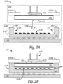
- FIGs. 2A-2B illustrate in cross-section a portion of test setup 100 at different stages of positioning probe assembly 150 using a spacer according to some embodiments.
- the spacer is embodied as collar spacers 155A.
- FIG. 2A illustrates probe assembly 150 and circuit assembly 120 when the fixture over-clamp (not shown) is in a raised position.
- FIG. 2B illustrates probe assembly 150 and circuit assembly 120 when the fixture over-clamp is in a probe assembly 150 and circuit assembly 120 when the fixture over-clamp is in a lowered position. In the lowered position, probe assembly 150 is partially inserted into a cavity formed within component 110.
- the collar spacers 155A contact surfaces 197 of housing 111 when sense plate 151 is distance 199 from pins 116. When probe assembly 150 is in the fully engaged position shown in FIG. 2B , capacitive testing of pins 116 may be performed.
- Collar spacers 155A may be configured to fully engage circuit assembly 120 when sense plate 151 is at any desired distance 199 from pins 116.
- collar spacers 155A are shown flat in the illustrated embodiment, "L" shaped collar spacers may be used to permit sense plate 151 to be positioned closer or further away from pins 116.
- a screw or other suitable adjustment mechanism may be used to adjust distance 199.
- a screw may control the position of collar spacers 155A relative to sense plate 151 in a direction perpendicular to the surface of sense plate 151.
- collar spacers 155A are shown connected to guard plate 153, collar spacers 155A may be integrated into probe assembly 150 in any suitable way. Collar spacers 155A may be positioned along the entire perimeter of probe assembly 150, along select portions of the perimeter, or at any suitable portion of probe assembly 150. For example, collar spacers 155A may be located at a few discrete portions of the perimeter of probe assembly 150 such as at corners, spaced along the perimeter, or on the underside of probe assembly 150. Collar spacers 155A are provided at enough locations to ensure that when probe assembly 150 is fully engaged the probe head is seated in a stable position. For example, spacers may be provided at at least three points around the perimeter of the probe to ensure stability.
- FIGs. 3A-3B illustrate in cross-section a portion of test setup 100 at different stages of positioning probe assembly 150 according to some other embodiments.
- the spacer is embodied as collar spacers 155B which are configured to engage surfaces 196 of substrate 130 instead of or in addition to surfaces 197 of housing 111.
- FIGs. 4A-4B illustrate in cross-sections a portion of test setup 100 at different stages of positioning probe assembly 150 according to some other embodiments.
- the spacer is again embodied as collar spacers 155B, though here collar spacers 155B only contacts surface 196 of substrate 130 when fully engaged. While in this example housing 111 is shown without a lip, housing 111 may have a lip portion even though collar spacers 155B only engages surface 196 of substrate 130.
- FIGs. 2A-4B have illustrated several embodiments of test setup 100 where the spacer is is part of a probe assembly. It should be appreciated that a spacer may engage any suitable combination of portions of component 110 and substrate 130. Different types of spacers may be used in conjunction with test setup 100 in any suitable way. While probe assembly 150 has been depicted as moving straight down in direction 198, it should be appreciated that movement to engage probe assembly 150 with circuit assembly 120 may take any suitable form. For example, probe assembly 150 may be attached to a hinged fixture over-clamp. Thus, probe assembly may move closer to component 110 in an arc or along any suitable path. It should be appreciated that probe assembly 150 need not move in an absolute sense. Rather, relative motion between the probe assembly 150 and component 110 can achieve the desired position of probe assembly 150 and component 110, even if such relative motion is achieved by motion of the circuit assembly relative to probe assembly 150.
- Risers 155C are positioned to extend below the surface of sense plate 151.
- the riser may be positioned along the entire perimeter of probe assembly 150, along select portions of the perimeter such as at the corners, spaced along the perimeter, on the underside of probe assembly 150, or at any suitable portion of probe assembly 150.
- Risers 155C may be positioned to contact any suitable surface.
- the risers are positioned to contact a surface 195 of component 110 devoid of pins 116.
- Surface 195 for example, could be around the perimeter of component 110 or in the center region of an LGA socket, such a region 114 ( FIG. 1B ).
- FIGs. 6A-6B show in cross-section a configuration similar to that shown in FIGs. 5A-5B .
- housing 111 of component 110 does not have a lip.
- FIGs. 7A-7B illustrate in cross-section a portion of test setup 100 where the spacer is configured as part of component 110.
- the spacer is embodied as housing spacers 155D which is formed as part of housing 111 of component 110.
- Housing spacers 155D are configured and arranged to prevent probe assembly 150 from contacting pins 116 when the probe assembly is inserted into the cavity of component 110.
- surfaces 194 contact a surface of probe assembly 150.
- Surface 194 may be positioned to extend above the upper surfaces of pins 116 by an amount that may be on the order of distance 199 ( FIG. 2B ).
- housing spacers 155D are shown along the perimeter of the cavity formed in component 110, housing spacers 155D may be configured as part of housing 111 in any suitable location.
- FIGs. 2A-7B have illustrated embodiments of test setup 100 using a spacer to vertically (e.g. perpendicular to the surface of the circuit assembly) position probe assembly 150 with respect to pins 116 of component 110. Lateral (e.g. parallel to the surface of the circuit assembly) positioning of probe assembly 150 may be controlled to ensure that probe assembly 150 appropriately fits within a cavity of a component housing and that spacers appropriately engage to establish a vertical position. Any suitable technique may be used to laterally position probe assembly 150 relative to a component containing a pin under test.
- lateral alignment may be achieved based on the shape of the spacer either alone or in combination with a compliant mechanism on probe assembly 150 that allows the lateral and/or vertical position of the probe assembly to be controlled by features on the probe assembly, a component and/or other parts of the circuit assembly.
- probe assembly 150 is shown to be mounted to over-clamp 193 through a compliance subassembly 156.
- Compliance subassembly 156 allows for lateral and vertical movement of the probe with respect to fixture over-clamp 193.
- compliance subassembly may additionally permit probe assembly 150 to rotate and/or tilt or move in other dimensions such that positioning of the probe assembly relative to a component under test is determined by alignment features.
- Compliance subassembly 156 in combination with guiding features that guide the probe assembly 150 into a desired position relative to a component to be tested, allows the positioning accuracy of the probe to be lower than the accuracy required to properly position the probe with respect to the pins of a component to be tested.
- compliance subassembly 156 uses springs 163 to allow compliant motion.
- compliance subassembly 156 is shown schematically to include a first member 164 rigidly coupled to over-clamp 193 and a second member 165 rigidly coupled to probe assembly 150.
- First member 164 and second member 165 are shown to be compliantly coupled through springs 163.
- compliant couplings may be used instead of or in addition to springs.
- Such compliant couplings may be formed from stretchable, bendable, or compressible materials, or any suitable complaint mechanism or combination of mechanisms.
- compliance subassembly 156 may include other components, such as fasteners to connect it to over-clamp 193, or members that limit the range of compliant motion of probe assembly 150.
- Compliance subassembly 156 may have different movement properties in the lateral direction than in the vertical direction and those movement properties need not be linear. For example, compliance subassembly 156 may more easily allow lateral movement than vertical movement. By allowing lateral movement with little resistance, compliance subassembly 156 may prevent the head of probe assembly 150 from getting "stuck" before spacers 155E are fully engaged and probe assembly 150 is properly positioned for testing component 110. On the other hand, a firm response to vertical pressure ensures that the spacers are fully engaged and the desired gap of distance 199 has been achieved.
- compliance subassembly 156 may permit vertical movement up to about 10.16 mm. Lateral movement of about 1.27 mm in any lateral direction may also be permitted. In various embodiments, compliance subassembly 156 allows movement in the vertical direction of at least 0.635, 1.27, 2.54, 5.08, 10.16 or 15.24 mm. In various embodiments, compliance subassembly 156 may allow movement in the lateral direction of at least 0.127, 0.254, 0.635, 1.27 or 2.54 mm. In some embodiments, compliance subassembly 156 returns probe assembly 150 to a neutral position when fixture over-clamp 193 is in the raised position.
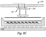
- FIG. 8A also provides an example of a spacer including guiding features that may be used to position a probe assembly. Guiding features may be implemented by appropriately shaping the surfaces contacted between probe assembly 150 and component 110 (and/or circuit assembly 120) when fixture over-clamp 193 is lowered to the test position. These surfaces may be beveled and/or tapered to guide probe assembly 150 to the desired measurement position. Though, surfaces of any suitable shape and position may be used.
- FIGs 8A-8C illustrate positioning of a probe assembly in an embodiment in which the spacer is embodied as beveled spacers 155E.
- Beveled spacers 155E include a beveled surface 188 positioned to engage a surface 187 with a complementary bevel on housing 111 of component 110. Interaction of beveled surfaces 187 and 188 may guide probe assembly 150 into alignment with pins 116 of component 110. As probe assembly 150 is lowered in direction 198, the guiding features, here the beveled surfaces 187 and 188 interact to provide alignment.
- the length of the beveled surfaces of may be selected to ensure that the maximum misalignment between probe assembly 150 and component 110 is accommodated.
- the maximum misalignment may be characteristic of the positioning accuracy of the fixture to which probe assembly 150 and circuit assembly 120 are attached. Misalignment of component 110 on circuit assembly 120 may also be a factor.
- the length of the beveled surface on probe assembly 150 and beveled surface on component 110 should be chosen to ensure the initial contact between the two is at the beveled surfaces.
- the surfaces are beveled with a steepness that ensures the friction between the contacted surfaces of probe assembly 150 and component 110 and the friction in compliance subassembly 156 is overcome. This allows probe assembly 150 to be properly laterally aligned with component 110 without getting stuck.
- a shallow bevel may be possible when there is low friction between the surfaces and within compliance subassembly 156.
- a steeper bevel relaxes the need for low friction, but may require component 110 have greater height.
- the surfaces are beveled at an angle 183 have a value of at least 10 or 30 degrees. Though, in other embodiments, the angle may be at least 20 or 30 degrees. In yet other embodiments, the surfaces will be beveled at an angle of about 45 degrees +/- 5 degrees.
- Compliance subassembly 156 allows probe assembly 150 to shift laterally to be properly aligned with pins 116 of component 110.
- probe assembly 150 may be attached to over-clamp 193 so that it is not initially aligned with its desired position relative to component 110.
- FIG. 8B as probe assembly 150 moves towards component 110, such as may occur when over-clamp 193 is closed to test a circuit assembly, the beveled surfaces will engage and, through a camming action associated with the motion of probe assembly 150 in direction 198, probe assembly 150 will move in direction 189.
- probe assembly 150 and component 110 may be vertically and laterally aligned for test measurements using a spacer and guiding features of any suitable configuration.
- FIGs. 8A-8C illustrated an embodiment of test setup 100 with beveled spacers to facilitate alignment.
- beveled surfaces may be integrated into only one of probe assembly 150 and component 110 or alternatively or additionally into a surface of a circuit assembly. Guiding features may be also tapered surfaces.
- FIGs. 9A-9E illustrate further examples of embodiments with guiding features of different shapes and positions.
- FIGs. 9A-9E do not illustrate a compliant mounting. However, the probe assemblies illustrated in these embodiments may similarly be used with a compliant mounting mechanism.
- FIG. 9A illustrates in cross-section an embodiment where probe assembly 150 includes wing spacers 155F which are beveled "wings" for aligning the probe with a component 110 having a lip portion 112 (see FIG. 3A ).
- Wing spacers 155F may extend beyond lip portion 112 such that each of the beveled wings, as probe assembly 150 moves towards a component under test, will contact a portion of lip 112, even if probe assembly 150 is not vertically aligned with the component.
- the beveled surfaces 186 of wing spacers 155F will slide along the upper portions of lip 112, generating a vertical force that moves probe assembly 150 into proper alignment for a sense plate on the probe assembly to appropriately enter a cavity of the component.
- the beveled wings also act as spacers, preventing the sense plate from contacting pins within the cavity once the probe assembly is partially inserted into the cavity. Because the vertical force will position probe assembly 150 with straight surfaces 185 contacting the upper surfaces of lip portion 112, wing spacers 155F can provide the same spacing as is illustrated in FIG. 2B .
- FIG. 9B illustrates another embodiment where probe assembly 150 includes spacers 155G which include a number of beveled and tapered surfaces that act as guiding features.
- the housing of a component may be adapted to receive probe assembly 150, as shown in FIG. 9B , such that when probe assembly 150 is fully engaged with the component, the probe's sense plate is properly aligned and spaced with respect to the pins in the component.
- FIG. 9C illustrates in cross-section another embodiment of probe assembly and component 110.
- tapered spears 155H in probe assembly 150 and conical holes in housing 111 serve and as guiding features and spacers for vertically and laterally aligning probe assembly 150 with component 110. Similar considerations as were made in choosing the width and slope of a beveled edges may be used in selecting the width and slope of the taper. For example, the slope of the taper should be steep enough to overcome friction between the tapered piece, the surface which it contacts, and the internal friction of the compliance assembly.
- FIG. 9D illustrates in cross-section yet another embodiment where guiding features and spacers are used to achieve lateral alignment and vertical alignment.
- spacers 155J have tapered spears which are used to provide lateral alignment and a collar ensure proper vertical alignment of probe assembly 150.
- FIG. 9E illustrates in cross-section a further example embodiment where holes drilled in substrate 130 are used to align probe assembly 150 with component 110.
- spacers 155K have a spear portion that provides lateral alignment with the holes in substrate 130 and a riser portion that contacts the surface of component 110 holding the sense plate the desired distance from the pins.
- spacers and/or guiding features for achieving lateral and/or vertical positioning of a probe assembly in close proximity to pins of a component may increase the strength of a signal coupled to a sense plate of the probe assembly. Consequently, more accurate testing may be performed.
- Another approach from improving testing accuracy is to provide a low-capacitance probe.
- FIG. 10A illustrates a cross section of a portion of a probe assembly 150.
- probe assembly 150 may further include a probe amplifier 154 electrically connected to sense plate 151.
- Probe amplifier 154 may be of any suitable design configured to amplify the response signal voltage detected on sense plate 151.
- probe amplifier 154 is a differential amplifier with a first terminal electrically connected by a first electrical lead to guard plate 153 and with a second terminal electrically connected by a second electrical lead to sense plate 151.
- probe amplifier 154 may be an operational amplifier. Though any suitable amplifier may be used.
- probe amplifier 154 may be augmented with a filter or designed to filter the response signal. The filter characteristics may be determined, for example, in accordance with the tests being performed or test signals being used.
- Sense plate 151 and guard plate 153 are capacitively coupled to each other through dielectric 152.
- the amplitude of the signal coupled to sense plate 151 from a pin under test may depend on the capacitance between sense plate 151 and guard plate 153. In some embodiments, it may be desirable to reduce the capacitance between sense plate 151 and guard plate 153 to provide a low capacitance probe.
- a low capacitance probe may be provided in any suitable way.
- a low capacitance between the sense and guard plates is achieved by reducing a total surface area of guard plate 153 by introducing holes in its surface.
- the voltage on sense plate 151 of the low capacitance probe is larger before amplification by probe amplifier 154. Accordingly, the response signal measured on a low capacitance probe may have a superior signal to noise ratio, leading to more accurate testing.
- the probe capacitance may also be reduced by increasing the thickness of dielectric 152 and/or using a low- ⁇ dielectric material.
- FIG. 10B-10C show a top view of guard plate 153 and a top view of sense plate 151, respectively.
- Sense plate 151 and guard plate 153 may have any suitable shape, but in the embodiments illustrated are substantially planar structures.
- guard plate 153 has a plurality of holes 157 reducing the overall surface area of guard plate 153 ( FIG. 10B ). Holes 157 may be formed in guard plate 153 in any suitable way and may be sized and positioned to reduce the capacitance between sense plate 151 and guard plate 153. In the example illustrated, circular holes are formed using known printed circuit board manufacturing techniques to remove conductive material from guard plate 153.
- the holes need not be filled with air. Any suitable approach that reduces the amount of conductive material at the surface of the guard plate 153 facing sense plate 151 may be used to form the holes.
- the holes may be formed by removing material, embossing the plate to move conductive material away from the surface, reducing the thickness of conductive material, or reducing the conductance of conductive material. Any of these techniques to create holes may be achieved by removing or changing material once in the form of a plate or by depositing or otherwise selectively depositing or otherwise positioning material over only selected portions of a region.
- guard plate 153 is separated from sense plate 151 by a distance, d, and each of holes 157 has a diameter greater than d.
- the holes may be circles with a diameter that is at least equal to the dielectric thickness 184. In some embodiments, the diameter may be 3 to 4 times the thickness. In yet some other embodiments, the diameter may be about 10 times the thickness. Though, the holes may have other shapes than circles. In some embodiments, whether or not the holes are circular, each hole 157 occupies an area of at least ⁇ ( n d / 2 ) 2 , where n may be, for example, 1, 3, 4, or 10.
- dielectric 152 has a thickness of about 1.27 mm and guard plate 153 has a plurality of circular holes each having a diameter of about 2.54 mm 2 .
- dielectric 152 has a thickness between 0.635 mm and 3.81 mm and the guard plate has holes each with a surface area in the range of 0.316 to 11.4 mm 2 .
- capacitance may be reduced by removing a portion 158 from guard plate 153 when probe assembly 150 is configured to test components having a center portion without pins.
- guard plate 153 may have a removed portion in its center region corresponding to the location in such a socket that is devoid of pins.
- a portion 159 may similarly be removed from sense plate 151 as shown in FIG. 10C . This removed portion may also correspond to a location in an LGA socket which is devoid of pins.
- portions 158 and 159 may each have a surface area of about 64.5, 161, 322 or 483 mm 2 , though, in some embodiments the area may be greater or smaller.
- portions 158 and 159 may each have dimensions of about 14.24 mm ⁇ 20.32 mm.
- FIGs. 11A-11B illustrate some additional embodiments of guard electrode 153 useful in a low capacitance probe.
- guard electrode 153 has holes 157 aligned vertically and horizontally in rows. As shown, the rows maybe parallel with one another and each row may include a plurality of holes 157. Holes 157 have a maximum dimension, D, and have an edge-to-edge spacing between adjacent member of a distance, S.
- D is in the range of 70 mils (1.8 mm) to 130 mils (3.3 mm) and S is in the range of 27 mils (0.7 mm) to 33 mils (0.8 mm).
- D is in the range of 1.27 mm to 2.54 mm and S is in the range of 0.254 to 0.762 mm. In some embodiments, D is in the range of 2.54 to 3.81 mm and S is in the range of 0.726 to 1.27 mm. Although any suitable value of D and S may be used.
- FIG. 11B illustrates another embodiment of guard plate 153.
- holes 157 are aligned in rows which are staggered.
- the center of each of holes 157A, 157B and 157C form 60° angles with respect to the other two centers.
- the rows are staggered such that an angle is created between a hole in a row and a nearest pair of holes in an adjacent row.
- the angle may be between 54° and 66°, or between 58° and 62°, or about 60°.
- sense plate 151 and guard plate 153 are shown having a square shape, it should be appreciated that they may take any suitable shape. In some embodiments, the plates are shaped to conform to a particular component to be tested.
- holes may take any shape and size.
- the holes could be triangles, squares, diamonds, ovals, or any other shape or combination of shapes.
- the holes may be arranged in a hatched pattern.
- holes 157 each have substantially the same size and shape. Though, in other embodiments, holes 157 need not be of the same size or shape. For example, holes may each have an irregular shape and have irregular spacing. Holes 157 may account for any suitable amount of the surface area of guard plate 153, as defined by the perimeter of the plate to reduce the capacitance as compared to a probe without holes 157 to a desired level.
- sense plate 151 and guard plate 153 may each have an area defined by there respective perimeters.
- the areas may be at least or at most 96.7, 322, 645 or 1935 mm 2 .
- the holes may account for at least or at most 10 percent of the total area. Though, in other embodiments, the holes may account for a larger percentage of the total area, such as at least 25, 40 or 50 percent of the total area.
- the capacitance between sense plate 151 and guard plate 153 is less than 100 picofarads (pF). In some embodiments, the capacitance is less than 35 pF. In some embodiments, the capacitance is in the range of 10 to 20 pF.
- test setup 100 methods of testing using test setup 100 and a method of manufacturing probe assembly 150 are briefly discussed with reference to FIGs. 12-14 .
- FIG. 12 is a flow chart of a method 200 of testing pins of a component.
- the probe assembly is coarsely aligned with the circuit assembly.
- the course alignment should be sufficient to ensure the alignment features between the probe assembly and circuit assembly are engaged when brought into contact with one another. Coarsely aligning the probe and circuit assembly may be performed, for example, placing the circuit assembly in a test fixture to which the probe is attached.
- the probe assembly and a component on the circuit assembly are moved together while allowing compliant motion based on the alignment features of the probe and/or circuit assembly.
- the probe and circuit assembly are brought into contact and the alignment features cause compliant motion of the probe providing lateral alignment of the probe with pins in the component of the circuit assembly.
- the probe assembly is partially inserted into the component.
- the component may have a cavity formed therein to which the probe is partially inserted.
- a socket may have a lip portion that surrounds part or all of the pins in the socket.
- the probe assembly is partially inserted into the component when at least a portion of the probe assembly is within the cavity formed in the component.
- the sense plate of the probe assembly may be inserted into the cavity.
- the spacer may be formed in any suitable way, for example, the spacer may be formed as a portion of the probe assembly, a portion of the component, a portion of the circuit assembly, or any suitable combination of the probe assembly, the component and the circuit assembly.
- the spacer may comprise alignment features which work in tandem with the spacer to provider vertical and lateral alignment of the probe assembly with the component. Insertion is fully restricted by the spacer when a sense plate of the probe assembly is a predetermined distance from the pins in the component. Different portions of the spacer may be used to provide vertical and lateral alignment of the probe assembly with the component.
- a signal coupled to the sense plate of the probe assembly is measured.
- the signal may be coupled in response to excitation of one or more pins under test in the component.
- the pins under test may be excited in any suitable way.
- the pin under test may be excited in accordance with capacitive opens testing techniques.
- the response signal is suitably amplified and filtered by the probe assembly.
- the measured signal may be analyzed to determine, for example, if a pin under test is properly connected to the circuit assembly.
- the magnitude of the measured signal may be compared to a threshold determined in a learn phase of testing. The result of comparing the magnitude with the threshold may be indicated through any suitable output device.
- step 206 a determination is made of whether there are any more tests to perform. For example, further tests may be performed to test other pins in the component. If another test is to be performed, method 200 returns to step 205 to conduct the subsequent test. If testing is complete, method 200 ends.
- FIG. 13 shows a flow chart of a method 300 for testing a circuit assembly using a low capacitance probe assembly.
- a test signal is driven on a signal line of the circuit assembly.
- the test signal may be supplied by a test system or by a virtual circuit generator. Any suitable electrical signal may be used as a test signal.
- a response signal coupled to a low capacitance probe having a guard plate with a plurality of holes is sensed.
- the response signal may be coupled to a sense plate of the probe, amplified and digitized by a test system for analysis.
- the holes on the low capacitance probe's guard plate may take any suitable form.
- the holes account for at least 25% of the total surface area of the guard plate as defined by the area within the perimeter of the guard plate.
- the holes account for at least 50% of the surface area.
- the total area of the holes is at least 40% of the surface area of the sense plate as defined by the area within the perimeter of the sense plate.
- the total area of the holes is at least 50% of the surface area of the sense plate as defined by the area within the perimeter of the sense plate.
- the holes may account for any suitable amount of guard plate surface area reduction.
- a test result is indicated based at least in part on the response signal measured at step 303.
- step 307 a determination is made as to whether there are any more tests to conduct. If the determination is yes, method 300 continues to step 301. If the determination is no, method 300 continues to step 309.
- step 309 subsequent steps in the manufacturing process are selected.
- the selection of the subsequent steps may be based, for example on the one or more test results indicated at step 305.
- Methods 200 and 300 may each be used as an intermediary step in a manufacturing process for circuit assemblies.
- the measurement and/or test results collected as a result of performing method 200 and 300 may be used for each circuit assembly to determine which subsequent steps in the manufacturing process are to be performed for that circuit assembly. For example, if all tests performed on the component yielded a positive result a determination may be made that the component has been properly installed on the circuit assembly. If some tests have failed, a decision may be made to conduct subsequent tests, to replace the component, or take another suitable action.
- method 200 is performed using a low capacitance probe assembly.
- FIG. 14 shows a flow chart of a method 400 for manufacturing a probe assembly.
- a sense plate is affixed to a first surface of a dielectric substrate.
- Sense plate may be affixed, for example, by gluing the plate to the dielectric substrate.
- a guard plate having a plurality of holes is formed and at step 405 the guard plate is affixed to a second surface of the dielectric substrate.
- Steps 403 and 405 may be performed in the order shown, in reverse order or performed simultaneously.
- a plate may be glued to the dielectric substrate and then etched or milled with the desired holes.
- the plate is deposited onto the dielectric substrate in a pattern with a plurality of holes.
- holes are formed through a plate which is then affixed to the dielectric substrate.
- the second surface is a surface substantially parallel to the first surface of the dielectric substrate.
- the guard plate has 10, 20, 50, 75, 100, 150 or 200 or more holes. Though, the guard plate may have any suitable number of holes.
- a first electrical lead is connected from the guard plate to a first terminal of an amplifier.
- a second electrical lead is connected from the sense plate to a second terminal of the amplifier.
- the second electrical lead is provided to the amplifier through one of the plurality of holes in the guard plate. More specifically a through hole through the dielectric substrate and the guard plate may be used to feed the second electrical lead from the sense plate to the amplifier.
- the lead is passed through a hole in the guard plate separate from the plurality of holes. The hole the lead is passed through may be a center removed region of the guard plate corresponding to a center region without pins as in some LGA socket connectors.
Landscapes
- Physics & Mathematics (AREA)
- General Physics & Mathematics (AREA)
- Engineering & Computer Science (AREA)
- General Engineering & Computer Science (AREA)
- Measuring Leads Or Probes (AREA)
Claims (16)
- Verfahren zum Prüfen jeder von mehreren verschiedenen Schaltungsanordnungen (120), wobei die Schaltungsanordnungen jeweils eine Komponente (110) mit einem Hohlraum und mehreren Stiften (116), die im Hohlraum angeordnet sind, umfassen und das Verfahren folgende Vorgänge umfasst:Einsetzen (203) einer Erfassungsplatte (151), die in einer Sonde, die ein Teil einer Sondenanordnung ist, enthalten ist, in den Hohlraum der Komponente (110), wodurch die Sondenanordnung in den Hohlraum teilweise eingesetzt wird undwobei der Vorgang des teilweisen Einsetzens der Sondenanordnung in den Hohlraum Folgendes umfasst:Bewegen der Sondenanordnung in einer ersten Richtung (198) zur Komponente (110),Erzeugen einer Kraft in einer zweiten Richtung (189) quer zur ersten Richtung (198) durch in Eingriff bringen mindestens einer abgeschrägten und/oder sich verjüngenden Führungsoberfläche zwischen der Sondenanordnung und der Komponente, wobei die abgeschrägte und/oder sich verjüngende Führungsoberfläche in die Sondenanordnung (150), die Komponente (110) oder eine Oberfläche einer Schaltungsanordnung (120) integriert ist, undAusrichten der Erfassungsplatte (151) im Hohlraum durch Ermöglichen einer Bewegung (150) der Sondenanordnung in der zweiten Querrichtung (189), während die Sondenanordnung sich in der ersten Richtung bewegt, wobei die Querbewegung durch eine Konformitätsbaugruppe (156) ermöglicht wird, die in der Sondenanordnung enthalten ist; undBeschränken (204) eines weiteren Einsetzens der Sondenanordnung (150) in der ersten Richtung mit einem Abstandshalter (155), um die Erfassungsplatte (151) im Bereich von 254 Mikrometern bis 2540 Mikrometern von den mehreren Stiften (116) zu positionieren, während ein Kontakt zwischen der Erfassungsplatte (151) der Sonde und den mehreren Stiften (116) ausgeschlossen wird.
- Verfahren nach Anspruch 1, wobeidie Komponente ein Gehäuse umfasst, das den Hohlraum begrenzt; undder Vorgang des Beschränkens ein Kontaktieren eines Kragenabschnitts der Sonde mit einem Lippenabschnitt des Gehäuses umfasst.
- Verfahren nach Anspruch 1, wobeider Abstandshalter einen Steigleitungsabschnitt der Sonde umfasst undder Vorgang des Beschränkens ein Kontaktieren des Abstandshalters mit einem Gehäuse der Komponente umfasst.
- Verfahren nach Anspruch 1, wobeider Abstandshalter einen Abschnitt eines Gehäuses (111) der Komponente umfasst undder Vorgang des Beschränkens ein Kontaktieren der Sonde mit dem Abschnitt des Gehäuses umfasst.
- Verfahren nach Anspruch 1, das ferner Folgendes umfasst:Erregen eines Prüfsignals auf einer Bahn der Schaltungsanordnung, die an den zu prüfenden Stift der Komponente gekoppelt ist;Messen einer Magnitude des Prüfsignals, das an die Sonde kapazitiv gekoppelt ist; und Angeben eines Prüfergebnisses auf der Grundlage der Magnitude des Prüfsignals, das an die Sonde gekoppelt ist.
- Prozess zum Herstellen einer Schaltungsanordnung, der Folgendes umfasst: Prüfen von Schaltungsanordnungen gemäß dem Verfahren nach Anspruch 5, wobei die Schaltungsanordnungen geprüft werden, nachdem ein erster Abschnitt des Herstellungsprozesses durchgeführt worden ist; und Wählen für jede Schaltungsanordnung, die geprüft wird, von Schritten in einem zweiten Abschnitt des Herstellungsprozesses auf der Grundlage des angegebenen Prüfergebnisses.
- Sondenanordnung zum Prüfen von mehreren Stiften (116), die an einer oberen Oberfläche einer Komponente (110) einer Schaltungsanordnung (120) freigelegt sind, wobei die Komponente (110) die mehreren Stifte (116) und ein Gehäuse (111) umfasst und die Sondenanordnung Folgendes umfasst:eine Erfassungsplatte (151), die aus einem Leitermaterial hergestellt ist;ein Dielektrikum; undeine Schutzplatte (153), die aus einem Leitermaterial hergestellt ist und von der Erfassungsplatte (151) durch das Dielektrikum (152) getrennt ist;dadurch gekennzeichnet, dass die Sondenanordnung ferner Folgendes umfasst:einen Abstandshalter (155), der an der Sondenanordnung angebracht ist, wobei der Abstandshalter bemessen und positioniert ist, um die Erfassungsplatte bei einer Prüfposition zu positionieren, bei der eine Lücke im Bereich von 254 Mikrometern bis 2540 Mikrometern von jedem Stift der mehreren Stifte vorhanden ist, und dennoch einen Kontakt der Erfassungsplatte mit den mehreren Stiften (116) auszuschließen, wenn die Erfassungsplatte in die Prüfposition bewegt wird und parallel zu und getrennt von der oberen Oberfläche angeordnet ist;ein Ausrichtungsmerkmal (186, 187, 188), das eine abgeschrägte und/oder sich verjüngende Führungsoberfläche aufweist, wobei das Ausrichtungsmerkmal bemessen und positioniert ist, mit der Schaltungsanordnung in Eingriff zu gelangen und die Erfassungsplatte in einer Richtung (189) quer zu einer Breite der Lücke auszurichten; undeine Konformitätsbaugruppe (156) zum Ermöglichen einer Querverlagerung der Erfassungsplatte in Bezug auf eine Befestigungsüberklemme (193), wenn das Ausrichtungsmerkmal mit der Schaltungsanordnung in Eingriff ist.
- Sondenanordnung nach Anspruch 7, wobeidie Komponente ein Gehäuse (111) umfasst, das einen Hohlraum aufweist, der darin gebildet ist, wobei der Hohlraum durch einen Abschnitt des Gehäuses um die mehreren Stifte, der einen Lippenabschnitt umfasst, begrenzt ist und die mehreren Stifte sich bei einer Basis des Hohlraums befinden; unddann, wenn die Erfassungsplatte und die mehreren Stifte durch die Lücke getrennt sind, die Sondenanordnung in den Hohlraum teilweise eingesetzt ist.
- Sondenanordnung nach Anspruch 8, wobei der Abstandshalter ein Kragenabschnitt der Sondenanordnung ist, der ausgelegt ist, den Lippenabschnitt zu berühren, wenn die Erfassungsplatte und die mehreren Stifte durch die Lücke getrennt sind.
- Sondenanordnung nach Anspruch 7, wobei der Abstandshalter ausgelegt ist, eine Oberfläche der Schaltungsanordnung zu berühren, wenn die Erfassungsplatte und die mehreren Stifte durch die Lücke getrennt sind.
- Sondenanordnung nach Anspruch 7, die ferner einen Verstärker umfasst, der ausgelegt ist, ein Signal zu verstärken, das an die Erfassungsplatte gekoppelt ist.
- System (100), das Folgendes umfasst:die Schaltungsanordnung (120), die die Komponente (110) mit mehreren Stiften aufweist; unddie Sondenanordnung (150) nach einem der Ansprüche 7 bis 11.
- System nach Anspruch 12, wobeidie mehreren Stifte in einem Hohlraum der Komponente angeordnet sind undder Abstandshalter an der Sondenanordnung angebracht ist und eine Oberfläche (195, 196) der Schaltungsanordnung berührt, wenn die Sondenanordnung in den Hohlraum teilweise eingesetzt ist und die Erfassungsplatte und die mehreren Stifte durch die Lücke getrennt sind.
- System nach Anspruch 12, wobei:
der Abstandshalter einen Abschnitt des Gehäuses bildet, der eine Oberfläche der Sondenanordnung berührt, wenn die Sondenanordnung in die Komponente teilweise eingesetzt ist und die Erfassungsplatte und die mehreren Stifte durch die Lücke getrennt sind. - System nach Anspruch 12, wobei der Abstandshalter das Ausrichtungsmerkmal zum Ausrichten der Sondenanordnung auf die Komponente in einer Querrichtung in Bezug auf eine Richtung der Lücke umfasst.
- Verfahren nach einem der Ansprüche 1 bis 5, Prozess nach Anspruch 6, Sondenanordnung nach einem der Ansprüche 7 bis 11 oder System nach einem der Ansprüche 12-15, wobei die Konformitätsbaugruppe (156) Federn (163) umfasst, um die Querverlagerung oder -bewegung zu ermöglichen.
Applications Claiming Priority (2)
| Application Number | Priority Date | Filing Date | Title |
|---|---|---|---|
| US12/645,418 US8310256B2 (en) | 2009-12-22 | 2009-12-22 | Capacitive opens testing in low signal environments |
| PCT/US2010/003238 WO2011087490A2 (en) | 2009-12-22 | 2010-12-21 | Capacitive opens testing in low signal environments |
Publications (3)
| Publication Number | Publication Date |
|---|---|
| EP2491409A2 EP2491409A2 (de) | 2012-08-29 |
| EP2491409A4 EP2491409A4 (de) | 2017-06-14 |
| EP2491409B1 true EP2491409B1 (de) | 2024-05-01 |
Family
ID=44150136
Family Applications (1)
| Application Number | Title | Priority Date | Filing Date |
|---|---|---|---|
| EP10843363.2A Active EP2491409B1 (de) | 2009-12-22 | 2010-12-21 | Testen kapazitiver öffnungen in umgebungen mit schwachen signalen |
Country Status (6)
| Country | Link |
|---|---|
| US (1) | US8310256B2 (de) |
| EP (1) | EP2491409B1 (de) |
| CN (1) | CN102667505B (de) |
| SG (1) | SG181443A1 (de) |
| TW (1) | TWI486603B (de) |
| WO (1) | WO2011087490A2 (de) |
Families Citing this family (15)
| Publication number | Priority date | Publication date | Assignee | Title |
|---|---|---|---|---|
| US8760185B2 (en) * | 2009-12-22 | 2014-06-24 | Anthony J. Suto | Low capacitance probe for testing circuit assembly |
| TW201249029A (en) * | 2011-05-20 | 2012-12-01 | Hon Hai Prec Ind Co Ltd | Controller IC adapter tool |
| US8933722B2 (en) * | 2011-08-31 | 2015-01-13 | Infineon Technologies Ag | Measuring device and a method for measuring a chip-to-chip-carrier connection |
| US8896320B2 (en) * | 2011-08-31 | 2014-11-25 | Infineon Technologies Ag | Measuring device and a method for measuring a chip-to-chip-carrier connection |
| TW201314233A (zh) * | 2011-09-21 | 2013-04-01 | Hon Hai Prec Ind Co Ltd | 測試卡 |
| TWI500945B (zh) * | 2013-12-17 | 2015-09-21 | Primax Electronics Ltd | 電路板之測試系統 |
| TWI614507B (zh) * | 2015-05-08 | 2018-02-11 | 宰體有限公司 | 測試插座用適配器 |
| US10615230B2 (en) | 2017-11-08 | 2020-04-07 | Teradyne, Inc. | Identifying potentially-defective picture elements in an active-matrix display panel |
| CN108710004A (zh) * | 2018-05-24 | 2018-10-26 | 苏州惠琪特电子科技有限公司 | 一种电子元器件测试装置 |
| JP7206140B2 (ja) * | 2019-03-22 | 2023-01-17 | 株式会社ヨコオ | 検査装置 |
| TWI717803B (zh) * | 2019-08-14 | 2021-02-01 | 日月光半導體製造股份有限公司 | 測試設備及測試方法 |
| TW202115413A (zh) * | 2019-09-30 | 2021-04-16 | 日商愛德萬測試股份有限公司 | 維護裝置、維護方法及記錄有維護程式之記錄媒體 |
| US11340260B2 (en) * | 2019-12-24 | 2022-05-24 | Teradyne, Inc. | Probe card pad geometry in automated test equipment |
| TWI737199B (zh) * | 2020-02-27 | 2021-08-21 | 黃文斌 | 電子元件測試夾具 |
| CN112986687B (zh) * | 2021-04-30 | 2021-09-10 | 成都宏明电子股份有限公司 | 具有表面电极的热敏电阻芯片筛选测试辅助工装 |
Family Cites Families (57)
| Publication number | Priority date | Publication date | Assignee | Title |
|---|---|---|---|---|
| US3975680A (en) * | 1975-06-25 | 1976-08-17 | Honeywell Information Systems, Inc. | Non-contact coupling plate for circuit board tester |
| GB8423310D0 (en) * | 1984-09-14 | 1984-10-17 | Gec Avionics | Electric circuit testing equipment |
| JPS63157076A (ja) | 1986-12-22 | 1988-06-30 | Matsushita Electric Ind Co Ltd | チツプテストポスト |
| US4868506A (en) * | 1988-12-02 | 1989-09-19 | International Business Machines Corporation | Defect detection using intermodulation signals |
| FR2660072B1 (fr) * | 1990-03-21 | 1992-07-24 | Int Market Dev | Appareil de test de circuit imprime. |
| US5254953A (en) * | 1990-12-20 | 1993-10-19 | Hewlett-Packard Company | Identification of pin-open faults by capacitive coupling through the integrated circuit package |
| US5557209A (en) | 1990-12-20 | 1996-09-17 | Hewlett-Packard Company | Identification of pin-open faults by capacitive coupling through the integrated circuit package |
| US5124660A (en) * | 1990-12-20 | 1992-06-23 | Hewlett-Packard Company | Identification of pin-open faults by capacitive coupling through the integrated circuit package |
| US5424633A (en) | 1991-01-22 | 1995-06-13 | Advanced Test Technologies Inc. | Contactless test method and system for testing printed circuit boards |
| CA2049616C (en) * | 1991-01-22 | 2000-04-04 | Jacob Soiferman | Contactless test method and system for testing printed circuit boards |
| US5696451A (en) | 1992-03-10 | 1997-12-09 | Hewlett-Packard Co. | Identification of pin-open faults by capacitive coupling |
| FR2697966B1 (fr) | 1992-11-06 | 1995-01-06 | Thomson Csf | Dispositif pour le test manuel d'une carte de circuit imprimé équipée de composants montés en surface. |
| US5420500A (en) * | 1992-11-25 | 1995-05-30 | Hewlett-Packard Company | Pacitive electrode system for detecting open solder joints in printed circuit assemblies |
| US5486753A (en) | 1993-07-30 | 1996-01-23 | Genrad, Inc. | Simultaneous capacitive open-circuit testing |
| US5530363A (en) | 1994-10-31 | 1996-06-25 | John Gaughan | DC ground fault detecting apparatus with an auto-null circuit and method |
| US5517110A (en) | 1995-04-06 | 1996-05-14 | Yentec Inc. | Contactless test method and system for testing printed circuit boards |
| DE69634376D1 (de) * | 1995-05-12 | 2005-03-31 | St Microelectronics Inc | IC-Packungsfassungssystem mit niedrigem Profil |
| US5747740A (en) | 1996-04-23 | 1998-05-05 | Gordon; William H. | Helical surface-mounted test point |
| US5986446A (en) * | 1997-02-05 | 1999-11-16 | C. Blake Williamson | Multi-meter and probe assembly and method of use |
| US6204680B1 (en) * | 1997-04-15 | 2001-03-20 | Delaware Capital Formation, Inc. | Test socket |
| US6104198A (en) | 1997-05-20 | 2000-08-15 | Zen Licensing Group Llp | Testing the integrity of an electrical connection to a device using an onboard controllable signal source |
| US6249052B1 (en) * | 1998-06-01 | 2001-06-19 | Paul T. Lin | Substrate on chip (SOC) multiple-chip module (MCM) with chip-size-package (CSP) ready configuration |
| US6243655B1 (en) | 1998-08-05 | 2001-06-05 | International Business Machines Corporation | Circuit trace probe and method |
| ATE346838T1 (de) | 1999-05-18 | 2006-12-15 | Sigma Tau Ind Farmaceuti | Verfahren zur herstellung von r-(-)-carnitin aus s-(-)-chlorbernsteinsäure oder aus einem ihrer derivate |
| WO2001090764A1 (en) * | 2000-05-22 | 2001-11-29 | Signus, Inc. | Method and apparatus for in-circuit impedance measurement |
| US6737875B2 (en) * | 2000-05-22 | 2004-05-18 | Damerco, Inc. | Method and apparatus for in-circuit impedance measurement |
| KR20020096094A (ko) * | 2001-06-16 | 2002-12-31 | 삼성전자 주식회사 | 테스터 헤드용 프로브 카드 |
| US7129714B2 (en) | 2002-07-02 | 2006-10-31 | Baxter Larry K | Capacitive measurement system |
| US6744267B2 (en) * | 2002-07-16 | 2004-06-01 | Nptest, Llc | Test system and methodology |
| US7279914B2 (en) * | 2003-01-17 | 2007-10-09 | Jsr Corporation | Circuit board checker and circuit board checking method |
| CN100469218C (zh) * | 2003-01-17 | 2009-03-11 | Jsr株式会社 | 用于电路板的检查设备和用于电路板的检查方法 |
| US7307222B2 (en) | 2003-09-24 | 2007-12-11 | Agilent Technologies, Inc. | Printed circuit board test access point structures and method for making the same |
| US6998849B2 (en) | 2003-09-27 | 2006-02-14 | Agilent Technologies, Inc. | Capacitive sensor measurement method for discrete time sampled system for in-circuit test |
| US6960917B2 (en) * | 2003-11-06 | 2005-11-01 | Agilent Technologies, Inc. | Methods and apparatus for diagnosing defect locations in electrical paths of connectors of circuit assemblies |
| JP2005233858A (ja) | 2004-02-23 | 2005-09-02 | Japan Electronic Materials Corp | プローブカード |
| US7208936B2 (en) * | 2004-04-12 | 2007-04-24 | Intel Corporation | Socket lid and test device |
| US7068039B2 (en) * | 2004-04-28 | 2006-06-27 | Agilent Technologies, Inc. | Test structure embedded in a shipping and handling cover for integrated circuit sockets and method for testing integrated circuit sockets and circuit assemblies utilizing same |
| US7123022B2 (en) * | 2004-04-28 | 2006-10-17 | Agilent Technologies, Inc. | Method and apparatus for non-contact testing and diagnosing electrical paths through connectors on circuit assemblies |
| US7161369B2 (en) | 2004-10-29 | 2007-01-09 | Agilent Technologies, Inc. | Method and apparatus for a wobble fixture probe for probing test access point structures |
| US20060103397A1 (en) | 2004-10-29 | 2006-05-18 | Parker Kenneth P | Method and apparatus for a twisting fixture probe for probing test access point structures |
| US7504589B2 (en) | 2004-10-25 | 2009-03-17 | Agilent Technologies, Inc. | Method and apparatus for manufacturing and probing printed circuit board test access point structures |
| US7190157B2 (en) | 2004-10-25 | 2007-03-13 | Agilent Technologies, Inc. | Method and apparatus for layout independent test point placement on a printed circuit board |
| US7224169B2 (en) | 2004-11-02 | 2007-05-29 | Agilent Technologies, Inc. | Methods and apparatus for non-contact testing and diagnosing of inaccessible shorted connections |
| US7619434B1 (en) * | 2004-12-01 | 2009-11-17 | Cardiac Pacemakers, Inc. | System for multiple layer printed circuit board misregistration testing |
| US20060129955A1 (en) | 2004-12-10 | 2006-06-15 | Jacobsen Chris R | Printed circuit board development cycle using probe location automation and bead probe technology |
| US7187165B2 (en) | 2004-12-10 | 2007-03-06 | Agilent Technologies, Inc. | Method and system for implicitly encoding preferred probing locations in a printed circuit board design for use in tester fixture build |
| US7129730B2 (en) * | 2004-12-15 | 2006-10-31 | Chipmos Technologies (Bermuda) Ltd. | Probe card assembly |
| US7518384B2 (en) | 2005-01-31 | 2009-04-14 | Agilent Technologies, Inc. | Method and apparatus for manufacturing and probing test probe access structures on vias |
| US7325219B2 (en) | 2005-02-16 | 2008-01-29 | Agilent Technologies, Inc. | Method and apparatus for determining probing locations for a printed circuit board |
| US7208957B2 (en) | 2005-03-01 | 2007-04-24 | Agilent Technologies, Inc. | Method for non-contact testing of fixed and inaccessible connections without using a sensor plate |
| US7057395B1 (en) | 2005-03-04 | 2006-06-06 | Agilent Technologies, Inc. | Method for diagnosing open defects on non-contacted nodes of an electronic device from measurements of capacitively coupled nodes |
| US7259576B2 (en) | 2005-03-14 | 2007-08-21 | Agilent Technologies, Inc. | Method and apparatus for a twisting fixture probe for probing test access point structures |
| US7075307B1 (en) | 2005-04-22 | 2006-07-11 | Agilent Technologies, Inc. | Method and apparatus for detecting shorts on inaccessible pins using capacitive measurements |
| CN101501509B (zh) * | 2005-06-10 | 2013-08-14 | 特拉华资本组成公司 | 具有柔性内互连件的电接触探针 |
| US7307427B2 (en) * | 2005-07-23 | 2007-12-11 | Agilent Technologies, Inc. | Method and apparatus for engineering a testability interposer for testing sockets and connectors on printed circuit boards |
| TWI320485B (en) * | 2007-03-08 | 2010-02-11 | Test Research Inc | Open-circuit testing system and method |
| US8211366B2 (en) * | 2009-08-24 | 2012-07-03 | Kee Gold Corp. | Apparatus and methods for testing impurity content in a precious metal |
-
2009
- 2009-12-22 US US12/645,418 patent/US8310256B2/en active Active
-
2010
- 2010-12-15 TW TW099143899A patent/TWI486603B/zh active
- 2010-12-21 WO PCT/US2010/003238 patent/WO2011087490A2/en not_active Ceased
- 2010-12-21 SG SG2012038691A patent/SG181443A1/en unknown
- 2010-12-21 CN CN201080058608.XA patent/CN102667505B/zh active Active
- 2010-12-21 EP EP10843363.2A patent/EP2491409B1/de active Active
Also Published As
| Publication number | Publication date |
|---|---|
| US8310256B2 (en) | 2012-11-13 |
| EP2491409A2 (de) | 2012-08-29 |
| US20110148446A1 (en) | 2011-06-23 |
| SG181443A1 (en) | 2012-07-30 |
| CN102667505B (zh) | 2015-04-01 |
| TWI486603B (zh) | 2015-06-01 |
| WO2011087490A3 (en) | 2011-11-17 |
| WO2011087490A2 (en) | 2011-07-21 |
| CN102667505A (zh) | 2012-09-12 |
| TW201142324A (en) | 2011-12-01 |
| EP2491409A4 (de) | 2017-06-14 |
Similar Documents
| Publication | Publication Date | Title |
|---|---|---|
| EP2491409B1 (de) | Testen kapazitiver öffnungen in umgebungen mit schwachen signalen | |
| US9778314B2 (en) | Capacitive opens testing of low profile components | |
| US10877090B2 (en) | Electrically conductive pins for microcircuit tester | |
| US10302675B2 (en) | Electrically conductive pins microcircuit tester | |
| CN102422726B (zh) | 用于微电路测试器的导电引脚 | |
| US8912811B2 (en) | Test contact system for testing integrated circuits with packages having an array of signal and power contacts | |
| US9007082B2 (en) | Electrically conductive pins for microcircuit tester | |
| US20140103949A1 (en) | Electrically Conductive Kelvin Contacts For Microcircuit Tester | |
| US8760185B2 (en) | Low capacitance probe for testing circuit assembly | |
| US8988090B2 (en) | Electrically conductive kelvin contacts for microcircuit tester | |
| US9606143B1 (en) | Electrically conductive pins for load boards lacking Kelvin capability for microcircuit testing |
Legal Events
| Date | Code | Title | Description |
|---|---|---|---|
| PUAI | Public reference made under article 153(3) epc to a published international application that has entered the european phase |
Free format text: ORIGINAL CODE: 0009012 |
|
| 17P | Request for examination filed |
Effective date: 20120523 |
|
| AK | Designated contracting states |
Kind code of ref document: A2 Designated state(s): AL AT BE BG CH CY CZ DE DK EE ES FI FR GB GR HR HU IE IS IT LI LT LU LV MC MK MT NL NO PL PT RO RS SE SI SK SM TR |
|
| DAX | Request for extension of the european patent (deleted) | ||
| A4 | Supplementary search report drawn up and despatched |
Effective date: 20170516 |
|
| RIC1 | Information provided on ipc code assigned before grant |
Ipc: G01R 31/04 20060101ALI20170510BHEP Ipc: G01R 31/312 20060101AFI20170510BHEP |
|
| STAA | Information on the status of an ep patent application or granted ep patent |
Free format text: STATUS: EXAMINATION IS IN PROGRESS |
|
| 17Q | First examination report despatched |
Effective date: 20200414 |
|
| RIC1 | Information provided on ipc code assigned before grant |
Ipc: G01R 31/312 20060101AFI20240123BHEP |
|
| GRAP | Despatch of communication of intention to grant a patent |
Free format text: ORIGINAL CODE: EPIDOSNIGR1 |
|
| STAA | Information on the status of an ep patent application or granted ep patent |
Free format text: STATUS: GRANT OF PATENT IS INTENDED |
|
| INTG | Intention to grant announced |
Effective date: 20240301 |
|
| GRAS | Grant fee paid |
Free format text: ORIGINAL CODE: EPIDOSNIGR3 |
|
| GRAA | (expected) grant |
Free format text: ORIGINAL CODE: 0009210 |
|
| STAA | Information on the status of an ep patent application or granted ep patent |
Free format text: STATUS: THE PATENT HAS BEEN GRANTED |
|
| AK | Designated contracting states |
Kind code of ref document: B1 Designated state(s): AL AT BE BG CH CY CZ DE DK EE ES FI FR GB GR HR HU IE IS IT LI LT LU LV MC MK MT NL NO PL PT RO RS SE SI SK SM TR |
|
| REG | Reference to a national code |
Ref country code: GB Ref legal event code: FG4D |
|
| P01 | Opt-out of the competence of the unified patent court (upc) registered |
Effective date: 20240404 |
|
| REG | Reference to a national code |
Ref country code: CH Ref legal event code: EP |
|
| REG | Reference to a national code |
Ref country code: DE Ref legal event code: R096 Ref document number: 602010069374 Country of ref document: DE |
|
| REG | Reference to a national code |
Ref country code: IE Ref legal event code: FG4D |
|
| REG | Reference to a national code |
Ref country code: LT Ref legal event code: MG9D |
|
| REG | Reference to a national code |
Ref country code: NL Ref legal event code: MP Effective date: 20240501 |
|
| PG25 | Lapsed in a contracting state [announced via postgrant information from national office to epo] |
Ref country code: IS Free format text: LAPSE BECAUSE OF FAILURE TO SUBMIT A TRANSLATION OF THE DESCRIPTION OR TO PAY THE FEE WITHIN THE PRESCRIBED TIME-LIMIT Effective date: 20240901 |
|
| PG25 | Lapsed in a contracting state [announced via postgrant information from national office to epo] |
Ref country code: BG Free format text: LAPSE BECAUSE OF FAILURE TO SUBMIT A TRANSLATION OF THE DESCRIPTION OR TO PAY THE FEE WITHIN THE PRESCRIBED TIME-LIMIT Effective date: 20240501 |
|
| PG25 | Lapsed in a contracting state [announced via postgrant information from national office to epo] |
Ref country code: FI Free format text: LAPSE BECAUSE OF FAILURE TO SUBMIT A TRANSLATION OF THE DESCRIPTION OR TO PAY THE FEE WITHIN THE PRESCRIBED TIME-LIMIT Effective date: 20240501 Ref country code: HR Free format text: LAPSE BECAUSE OF FAILURE TO SUBMIT A TRANSLATION OF THE DESCRIPTION OR TO PAY THE FEE WITHIN THE PRESCRIBED TIME-LIMIT Effective date: 20240501 |
|
| PG25 | Lapsed in a contracting state [announced via postgrant information from national office to epo] |
Ref country code: GR Free format text: LAPSE BECAUSE OF FAILURE TO SUBMIT A TRANSLATION OF THE DESCRIPTION OR TO PAY THE FEE WITHIN THE PRESCRIBED TIME-LIMIT Effective date: 20240802 |
|
| PG25 | Lapsed in a contracting state [announced via postgrant information from national office to epo] |
Ref country code: PT Free format text: LAPSE BECAUSE OF FAILURE TO SUBMIT A TRANSLATION OF THE DESCRIPTION OR TO PAY THE FEE WITHIN THE PRESCRIBED TIME-LIMIT Effective date: 20240902 |
|
| REG | Reference to a national code |
Ref country code: AT Ref legal event code: MK05 Ref document number: 1683069 Country of ref document: AT Kind code of ref document: T Effective date: 20240501 |
|
| PG25 | Lapsed in a contracting state [announced via postgrant information from national office to epo] |
Ref country code: NL Free format text: LAPSE BECAUSE OF FAILURE TO SUBMIT A TRANSLATION OF THE DESCRIPTION OR TO PAY THE FEE WITHIN THE PRESCRIBED TIME-LIMIT Effective date: 20240501 |
|
| PG25 | Lapsed in a contracting state [announced via postgrant information from national office to epo] |
Ref country code: ES Free format text: LAPSE BECAUSE OF FAILURE TO SUBMIT A TRANSLATION OF THE DESCRIPTION OR TO PAY THE FEE WITHIN THE PRESCRIBED TIME-LIMIT Effective date: 20240501 |
|
| PG25 | Lapsed in a contracting state [announced via postgrant information from national office to epo] |
Ref country code: AT Free format text: LAPSE BECAUSE OF FAILURE TO SUBMIT A TRANSLATION OF THE DESCRIPTION OR TO PAY THE FEE WITHIN THE PRESCRIBED TIME-LIMIT Effective date: 20240501 |
|
| PG25 | Lapsed in a contracting state [announced via postgrant information from national office to epo] |
Ref country code: PL Free format text: LAPSE BECAUSE OF FAILURE TO SUBMIT A TRANSLATION OF THE DESCRIPTION OR TO PAY THE FEE WITHIN THE PRESCRIBED TIME-LIMIT Effective date: 20240501 |
|
| PG25 | Lapsed in a contracting state [announced via postgrant information from national office to epo] |
Ref country code: LV Free format text: LAPSE BECAUSE OF FAILURE TO SUBMIT A TRANSLATION OF THE DESCRIPTION OR TO PAY THE FEE WITHIN THE PRESCRIBED TIME-LIMIT Effective date: 20240501 |
|
| PG25 | Lapsed in a contracting state [announced via postgrant information from national office to epo] |
Ref country code: PT Free format text: LAPSE BECAUSE OF FAILURE TO SUBMIT A TRANSLATION OF THE DESCRIPTION OR TO PAY THE FEE WITHIN THE PRESCRIBED TIME-LIMIT Effective date: 20240902 Ref country code: PL Free format text: LAPSE BECAUSE OF FAILURE TO SUBMIT A TRANSLATION OF THE DESCRIPTION OR TO PAY THE FEE WITHIN THE PRESCRIBED TIME-LIMIT Effective date: 20240501 Ref country code: NO Free format text: LAPSE BECAUSE OF FAILURE TO SUBMIT A TRANSLATION OF THE DESCRIPTION OR TO PAY THE FEE WITHIN THE PRESCRIBED TIME-LIMIT Effective date: 20240801 Ref country code: NL Free format text: LAPSE BECAUSE OF FAILURE TO SUBMIT A TRANSLATION OF THE DESCRIPTION OR TO PAY THE FEE WITHIN THE PRESCRIBED TIME-LIMIT Effective date: 20240501 Ref country code: LV Free format text: LAPSE BECAUSE OF FAILURE TO SUBMIT A TRANSLATION OF THE DESCRIPTION OR TO PAY THE FEE WITHIN THE PRESCRIBED TIME-LIMIT Effective date: 20240501 Ref country code: IS Free format text: LAPSE BECAUSE OF FAILURE TO SUBMIT A TRANSLATION OF THE DESCRIPTION OR TO PAY THE FEE WITHIN THE PRESCRIBED TIME-LIMIT Effective date: 20240901 Ref country code: HR Free format text: LAPSE BECAUSE OF FAILURE TO SUBMIT A TRANSLATION OF THE DESCRIPTION OR TO PAY THE FEE WITHIN THE PRESCRIBED TIME-LIMIT Effective date: 20240501 Ref country code: GR Free format text: LAPSE BECAUSE OF FAILURE TO SUBMIT A TRANSLATION OF THE DESCRIPTION OR TO PAY THE FEE WITHIN THE PRESCRIBED TIME-LIMIT Effective date: 20240802 Ref country code: FI Free format text: LAPSE BECAUSE OF FAILURE TO SUBMIT A TRANSLATION OF THE DESCRIPTION OR TO PAY THE FEE WITHIN THE PRESCRIBED TIME-LIMIT Effective date: 20240501 Ref country code: ES Free format text: LAPSE BECAUSE OF FAILURE TO SUBMIT A TRANSLATION OF THE DESCRIPTION OR TO PAY THE FEE WITHIN THE PRESCRIBED TIME-LIMIT Effective date: 20240501 Ref country code: BG Free format text: LAPSE BECAUSE OF FAILURE TO SUBMIT A TRANSLATION OF THE DESCRIPTION OR TO PAY THE FEE WITHIN THE PRESCRIBED TIME-LIMIT Effective date: 20240501 Ref country code: AT Free format text: LAPSE BECAUSE OF FAILURE TO SUBMIT A TRANSLATION OF THE DESCRIPTION OR TO PAY THE FEE WITHIN THE PRESCRIBED TIME-LIMIT Effective date: 20240501 Ref country code: RS Free format text: LAPSE BECAUSE OF FAILURE TO SUBMIT A TRANSLATION OF THE DESCRIPTION OR TO PAY THE FEE WITHIN THE PRESCRIBED TIME-LIMIT Effective date: 20240801 |
|
| PG25 | Lapsed in a contracting state [announced via postgrant information from national office to epo] |
Ref country code: DK Free format text: LAPSE BECAUSE OF FAILURE TO SUBMIT A TRANSLATION OF THE DESCRIPTION OR TO PAY THE FEE WITHIN THE PRESCRIBED TIME-LIMIT Effective date: 20240501 |
|
| PG25 | Lapsed in a contracting state [announced via postgrant information from national office to epo] |
Ref country code: EE Free format text: LAPSE BECAUSE OF FAILURE TO SUBMIT A TRANSLATION OF THE DESCRIPTION OR TO PAY THE FEE WITHIN THE PRESCRIBED TIME-LIMIT Effective date: 20240501 |
|
| PG25 | Lapsed in a contracting state [announced via postgrant information from national office to epo] |
Ref country code: CZ Free format text: LAPSE BECAUSE OF FAILURE TO SUBMIT A TRANSLATION OF THE DESCRIPTION OR TO PAY THE FEE WITHIN THE PRESCRIBED TIME-LIMIT Effective date: 20240501 |
|
| PG25 | Lapsed in a contracting state [announced via postgrant information from national office to epo] |
Ref country code: RO Free format text: LAPSE BECAUSE OF FAILURE TO SUBMIT A TRANSLATION OF THE DESCRIPTION OR TO PAY THE FEE WITHIN THE PRESCRIBED TIME-LIMIT Effective date: 20240501 Ref country code: SK Free format text: LAPSE BECAUSE OF FAILURE TO SUBMIT A TRANSLATION OF THE DESCRIPTION OR TO PAY THE FEE WITHIN THE PRESCRIBED TIME-LIMIT Effective date: 20240501 |
|
| PG25 | Lapsed in a contracting state [announced via postgrant information from national office to epo] |
Ref country code: SM Free format text: LAPSE BECAUSE OF FAILURE TO SUBMIT A TRANSLATION OF THE DESCRIPTION OR TO PAY THE FEE WITHIN THE PRESCRIBED TIME-LIMIT Effective date: 20240501 |
|
| PG25 | Lapsed in a contracting state [announced via postgrant information from national office to epo] |
Ref country code: SM Free format text: LAPSE BECAUSE OF FAILURE TO SUBMIT A TRANSLATION OF THE DESCRIPTION OR TO PAY THE FEE WITHIN THE PRESCRIBED TIME-LIMIT Effective date: 20240501 Ref country code: SK Free format text: LAPSE BECAUSE OF FAILURE TO SUBMIT A TRANSLATION OF THE DESCRIPTION OR TO PAY THE FEE WITHIN THE PRESCRIBED TIME-LIMIT Effective date: 20240501 Ref country code: RO Free format text: LAPSE BECAUSE OF FAILURE TO SUBMIT A TRANSLATION OF THE DESCRIPTION OR TO PAY THE FEE WITHIN THE PRESCRIBED TIME-LIMIT Effective date: 20240501 Ref country code: EE Free format text: LAPSE BECAUSE OF FAILURE TO SUBMIT A TRANSLATION OF THE DESCRIPTION OR TO PAY THE FEE WITHIN THE PRESCRIBED TIME-LIMIT Effective date: 20240501 Ref country code: DK Free format text: LAPSE BECAUSE OF FAILURE TO SUBMIT A TRANSLATION OF THE DESCRIPTION OR TO PAY THE FEE WITHIN THE PRESCRIBED TIME-LIMIT Effective date: 20240501 Ref country code: CZ Free format text: LAPSE BECAUSE OF FAILURE TO SUBMIT A TRANSLATION OF THE DESCRIPTION OR TO PAY THE FEE WITHIN THE PRESCRIBED TIME-LIMIT Effective date: 20240501 |
|
| REG | Reference to a national code |
Ref country code: DE Ref legal event code: R097 Ref document number: 602010069374 Country of ref document: DE |
|
| PG25 | Lapsed in a contracting state [announced via postgrant information from national office to epo] |
Ref country code: IT Free format text: LAPSE BECAUSE OF FAILURE TO SUBMIT A TRANSLATION OF THE DESCRIPTION OR TO PAY THE FEE WITHIN THE PRESCRIBED TIME-LIMIT Effective date: 20240501 |
|
| PLBE | No opposition filed within time limit |
Free format text: ORIGINAL CODE: 0009261 |
|
| STAA | Information on the status of an ep patent application or granted ep patent |
Free format text: STATUS: NO OPPOSITION FILED WITHIN TIME LIMIT |
|
| 26N | No opposition filed |
Effective date: 20250204 |
|
| PG25 | Lapsed in a contracting state [announced via postgrant information from national office to epo] |
Ref country code: SI Free format text: LAPSE BECAUSE OF FAILURE TO SUBMIT A TRANSLATION OF THE DESCRIPTION OR TO PAY THE FEE WITHIN THE PRESCRIBED TIME-LIMIT Effective date: 20240501 |
|
| PG25 | Lapsed in a contracting state [announced via postgrant information from national office to epo] |
Ref country code: MC Free format text: LAPSE BECAUSE OF FAILURE TO SUBMIT A TRANSLATION OF THE DESCRIPTION OR TO PAY THE FEE WITHIN THE PRESCRIBED TIME-LIMIT Effective date: 20240501 |
|
| REG | Reference to a national code |
Ref country code: CH Ref legal event code: PL |
|
| PG25 | Lapsed in a contracting state [announced via postgrant information from national office to epo] |
Ref country code: LU Free format text: LAPSE BECAUSE OF NON-PAYMENT OF DUE FEES Effective date: 20241221 |
|
| PG25 | Lapsed in a contracting state [announced via postgrant information from national office to epo] |
Ref country code: SE Free format text: LAPSE BECAUSE OF FAILURE TO SUBMIT A TRANSLATION OF THE DESCRIPTION OR TO PAY THE FEE WITHIN THE PRESCRIBED TIME-LIMIT Effective date: 20240501 |
|
| REG | Reference to a national code |
Ref country code: BE Ref legal event code: MM Effective date: 20241231 |
|
| PG25 | Lapsed in a contracting state [announced via postgrant information from national office to epo] |
Ref country code: BE Free format text: LAPSE BECAUSE OF NON-PAYMENT OF DUE FEES Effective date: 20241231 |
|
| PG25 | Lapsed in a contracting state [announced via postgrant information from national office to epo] |
Ref country code: CH Free format text: LAPSE BECAUSE OF NON-PAYMENT OF DUE FEES Effective date: 20241231 |
|
| PG25 | Lapsed in a contracting state [announced via postgrant information from national office to epo] |
Ref country code: IE Free format text: LAPSE BECAUSE OF NON-PAYMENT OF DUE FEES Effective date: 20241221 |
|
| PGFP | Annual fee paid to national office [announced via postgrant information from national office to epo] |
Ref country code: DE Payment date: 20250930 Year of fee payment: 16 |
|
| PGFP | Annual fee paid to national office [announced via postgrant information from national office to epo] |
Ref country code: GB Payment date: 20251001 Year of fee payment: 16 |
|
| PGFP | Annual fee paid to national office [announced via postgrant information from national office to epo] |
Ref country code: FR Payment date: 20251008 Year of fee payment: 16 |