EP2485248B1 - Film forming method using catalytic cvd device - Google Patents
Film forming method using catalytic cvd device Download PDFInfo
- Publication number
- EP2485248B1 EP2485248B1 EP10820725.9A EP10820725A EP2485248B1 EP 2485248 B1 EP2485248 B1 EP 2485248B1 EP 10820725 A EP10820725 A EP 10820725A EP 2485248 B1 EP2485248 B1 EP 2485248B1
- Authority
- EP
- European Patent Office
- Prior art keywords
- catalytic
- temperature
- film
- substrate
- wire
- Prior art date
- Legal status (The legal status is an assumption and is not a legal conclusion. Google has not performed a legal analysis and makes no representation as to the accuracy of the status listed.)
- Active
Links
Images
Classifications
-
- C—CHEMISTRY; METALLURGY
- C23—COATING METALLIC MATERIAL; COATING MATERIAL WITH METALLIC MATERIAL; CHEMICAL SURFACE TREATMENT; DIFFUSION TREATMENT OF METALLIC MATERIAL; COATING BY VACUUM EVAPORATION, BY SPUTTERING, BY ION IMPLANTATION OR BY CHEMICAL VAPOUR DEPOSITION, IN GENERAL; INHIBITING CORROSION OF METALLIC MATERIAL OR INCRUSTATION IN GENERAL
- C23C—COATING METALLIC MATERIAL; COATING MATERIAL WITH METALLIC MATERIAL; SURFACE TREATMENT OF METALLIC MATERIAL BY DIFFUSION INTO THE SURFACE, BY CHEMICAL CONVERSION OR SUBSTITUTION; COATING BY VACUUM EVAPORATION, BY SPUTTERING, BY ION IMPLANTATION OR BY CHEMICAL VAPOUR DEPOSITION, IN GENERAL
- C23C16/00—Chemical coating by decomposition of gaseous compounds, without leaving reaction products of surface material in the coating, i.e. chemical vapour deposition [CVD] processes
- C23C16/44—Chemical coating by decomposition of gaseous compounds, without leaving reaction products of surface material in the coating, i.e. chemical vapour deposition [CVD] processes characterised by the method of coating
- C23C16/448—Chemical coating by decomposition of gaseous compounds, without leaving reaction products of surface material in the coating, i.e. chemical vapour deposition [CVD] processes characterised by the method of coating characterised by the method used for generating reactive gas streams, e.g. by evaporation or sublimation of precursor materials
- C23C16/4488—Chemical coating by decomposition of gaseous compounds, without leaving reaction products of surface material in the coating, i.e. chemical vapour deposition [CVD] processes characterised by the method of coating characterised by the method used for generating reactive gas streams, e.g. by evaporation or sublimation of precursor materials by in situ generation of reactive gas by chemical or electrochemical reaction
-
- C—CHEMISTRY; METALLURGY
- C23—COATING METALLIC MATERIAL; COATING MATERIAL WITH METALLIC MATERIAL; CHEMICAL SURFACE TREATMENT; DIFFUSION TREATMENT OF METALLIC MATERIAL; COATING BY VACUUM EVAPORATION, BY SPUTTERING, BY ION IMPLANTATION OR BY CHEMICAL VAPOUR DEPOSITION, IN GENERAL; INHIBITING CORROSION OF METALLIC MATERIAL OR INCRUSTATION IN GENERAL
- C23C—COATING METALLIC MATERIAL; COATING MATERIAL WITH METALLIC MATERIAL; SURFACE TREATMENT OF METALLIC MATERIAL BY DIFFUSION INTO THE SURFACE, BY CHEMICAL CONVERSION OR SUBSTITUTION; COATING BY VACUUM EVAPORATION, BY SPUTTERING, BY ION IMPLANTATION OR BY CHEMICAL VAPOUR DEPOSITION, IN GENERAL
- C23C16/00—Chemical coating by decomposition of gaseous compounds, without leaving reaction products of surface material in the coating, i.e. chemical vapour deposition [CVD] processes
- C23C16/22—Chemical coating by decomposition of gaseous compounds, without leaving reaction products of surface material in the coating, i.e. chemical vapour deposition [CVD] processes characterised by the deposition of inorganic material, other than metallic material
- C23C16/24—Deposition of silicon only
-
- C—CHEMISTRY; METALLURGY
- C23—COATING METALLIC MATERIAL; COATING MATERIAL WITH METALLIC MATERIAL; CHEMICAL SURFACE TREATMENT; DIFFUSION TREATMENT OF METALLIC MATERIAL; COATING BY VACUUM EVAPORATION, BY SPUTTERING, BY ION IMPLANTATION OR BY CHEMICAL VAPOUR DEPOSITION, IN GENERAL; INHIBITING CORROSION OF METALLIC MATERIAL OR INCRUSTATION IN GENERAL
- C23C—COATING METALLIC MATERIAL; COATING MATERIAL WITH METALLIC MATERIAL; SURFACE TREATMENT OF METALLIC MATERIAL BY DIFFUSION INTO THE SURFACE, BY CHEMICAL CONVERSION OR SUBSTITUTION; COATING BY VACUUM EVAPORATION, BY SPUTTERING, BY ION IMPLANTATION OR BY CHEMICAL VAPOUR DEPOSITION, IN GENERAL
- C23C16/00—Chemical coating by decomposition of gaseous compounds, without leaving reaction products of surface material in the coating, i.e. chemical vapour deposition [CVD] processes
- C23C16/44—Chemical coating by decomposition of gaseous compounds, without leaving reaction products of surface material in the coating, i.e. chemical vapour deposition [CVD] processes characterised by the method of coating
-
- H—ELECTRICITY
- H10—SEMICONDUCTOR DEVICES; ELECTRIC SOLID-STATE DEVICES NOT OTHERWISE PROVIDED FOR
- H10F—INORGANIC SEMICONDUCTOR DEVICES SENSITIVE TO INFRARED RADIATION, LIGHT, ELECTROMAGNETIC RADIATION OF SHORTER WAVELENGTH OR CORPUSCULAR RADIATION
- H10F10/00—Individual photovoltaic cells, e.g. solar cells
-
- H—ELECTRICITY
- H10—SEMICONDUCTOR DEVICES; ELECTRIC SOLID-STATE DEVICES NOT OTHERWISE PROVIDED FOR
- H10P—GENERIC PROCESSES OR APPARATUS FOR THE MANUFACTURE OR TREATMENT OF DEVICES COVERED BY CLASS H10
- H10P14/00—Formation of materials, e.g. in the shape of layers or pillars
- H10P14/20—Formation of materials, e.g. in the shape of layers or pillars of semiconductor materials
- H10P14/24—Formation of materials, e.g. in the shape of layers or pillars of semiconductor materials using chemical vapour deposition [CVD]
-
- H—ELECTRICITY
- H10—SEMICONDUCTOR DEVICES; ELECTRIC SOLID-STATE DEVICES NOT OTHERWISE PROVIDED FOR
- H10P—GENERIC PROCESSES OR APPARATUS FOR THE MANUFACTURE OR TREATMENT OF DEVICES COVERED BY CLASS H10
- H10P14/00—Formation of materials, e.g. in the shape of layers or pillars
- H10P14/20—Formation of materials, e.g. in the shape of layers or pillars of semiconductor materials
- H10P14/29—Formation of materials, e.g. in the shape of layers or pillars of semiconductor materials characterised by the substrates
- H10P14/2901—Materials
- H10P14/2922—Materials being non-crystalline insulating materials, e.g. glass or polymers
-
- H—ELECTRICITY
- H10—SEMICONDUCTOR DEVICES; ELECTRIC SOLID-STATE DEVICES NOT OTHERWISE PROVIDED FOR
- H10P—GENERIC PROCESSES OR APPARATUS FOR THE MANUFACTURE OR TREATMENT OF DEVICES COVERED BY CLASS H10
- H10P14/00—Formation of materials, e.g. in the shape of layers or pillars
- H10P14/20—Formation of materials, e.g. in the shape of layers or pillars of semiconductor materials
- H10P14/34—Deposited materials, e.g. layers
- H10P14/3402—Deposited materials, e.g. layers characterised by the chemical composition
- H10P14/3404—Deposited materials, e.g. layers characterised by the chemical composition being Group IVA materials
- H10P14/3411—Silicon, silicon germanium or germanium
-
- H—ELECTRICITY
- H10—SEMICONDUCTOR DEVICES; ELECTRIC SOLID-STATE DEVICES NOT OTHERWISE PROVIDED FOR
- H10P—GENERIC PROCESSES OR APPARATUS FOR THE MANUFACTURE OR TREATMENT OF DEVICES COVERED BY CLASS H10
- H10P14/00—Formation of materials, e.g. in the shape of layers or pillars
- H10P14/20—Formation of materials, e.g. in the shape of layers or pillars of semiconductor materials
- H10P14/34—Deposited materials, e.g. layers
- H10P14/3451—Structure
- H10P14/3452—Microstructure
- H10P14/3454—Amorphous
-
- Y—GENERAL TAGGING OF NEW TECHNOLOGICAL DEVELOPMENTS; GENERAL TAGGING OF CROSS-SECTIONAL TECHNOLOGIES SPANNING OVER SEVERAL SECTIONS OF THE IPC; TECHNICAL SUBJECTS COVERED BY FORMER USPC CROSS-REFERENCE ART COLLECTIONS [XRACs] AND DIGESTS
- Y02—TECHNOLOGIES OR APPLICATIONS FOR MITIGATION OR ADAPTATION AGAINST CLIMATE CHANGE
- Y02E—REDUCTION OF GREENHOUSE GAS [GHG] EMISSIONS, RELATED TO ENERGY GENERATION, TRANSMISSION OR DISTRIBUTION
- Y02E10/00—Energy generation through renewable energy sources
- Y02E10/50—Photovoltaic [PV] energy
Definitions
- the present invention relates to using catalytic CVD equipment for forming a film on a substrate.
- a CVD technique (a Chemical Vapor Deposition technique) is conventionally known.
- a catalytic CVD technique utilizing Catalytic Chemical Vapor Deposition has been discussed (Patent Document 1, for example).
- a raw material gas to be supplied into a reaction chamber is decomposed by employing a catalytic wire that is made of heated tungsten, molybdenum or the like and then a deposited film is formed on a substrate that is held on a holder.
- the catalytic CVD technique is expected as a method for formation of film, by which a substrate surface or a deposited film surface is less adversely affected, since such plasma discharge in a plasma CVD technique is not utilized.
- US2005/268852 discloses a vacuum film-forming apparatus comprising substrate stages; vacuum chamber-forming containers opposed to the stages; a means for moving the substrate between the stages; and gas-introduction means connected to every container, wherein one of the stage and the container is ascended or descended towards the other to bring the upper face of the stage and the opening of the container into contact with one another so that vacuum chambers can be formed and that a raw gas and/or a reactant gas can be introduced into each space of the chamber through each gas-introduction means to carry out either the adsorption or reaction step for allowing the raw gas to react with the reactant gas.
- Patent Document 1 Japanese Unexamined Patent Application Publication No. 2005-327995
- the present invention has been made to solve the above-described problem, and it is an object of the present invention to provide a method for formation of film which is capable of realizing extended serviceable life of a catalytic wire.
- the method according to the present invention is capable of maintaining a temperature of a catalytic wire at a predetermined temperature which is lower than a temperature when the film is formed, and is higher than room temperature at each of predetermined time intervals before and after the film is formed. Therefore, according to the present invention, shrinkage and expansion of the catalytic wire can be mitigated, thus making it possible to realize extended serviceable life of the catalytic wire.
- the method according to the present invention may optionally be as specified in any one of claims 2 to 4.
- the present inventors made their utmost efforts in study with respect to why the catalytic wire easily breaks. As a result, it was determined that there had been a problem in that power supply to the catalytic wire is stopped after the completion of formation of film and then power supply to the catalytic wire is started again at the time of start of formation of film.
- a temperature of the catalytic wire lowers from a temperature when the film is formed (for example, 1,600 degrees Centigrade to 2,000 degrees Centigrade) to the order of room temperature within several seconds due to a small thermal capacity of the catalytic wire; and therefore, the catalytic wire rapidly shrinks.
- the temperature of the catalytic wire rises from the order of room temperature to the temperature when the film is formed within several seconds; and therefore, the catalytic wire rapidly expands. It was determined that such shrinkage and expansion are repeated every time stop and start of power supply is switched, thereby reducing serviceable life of the catalytic wire.
- the present invention contrives control of power supply to a catalytic wire to thereby realize extended serviceable life of the catalytic wire.
- control of power supply to the catalytic wire focusing on control of power supply to the catalytic wire.
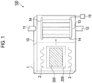
- Fig. 1 is a schematic diagram showing a configuration of a catalytic CVD equipment 100.
- the catalytic CVD equipment 100 has a preparation chamber 1, a reaction chamber 10, and a takeout chamber (not shown).
- a substrate 300 that is held on a substrate tray 200 is moved from the preparation chamber 1 to the reaction chamber 10, making it possible to form a deposited film on the substrate 300.
- the preparation chamber 1, the reaction chamber 10, and the takeout chamber are evacuated at a pressure lower than about 1 x 10 -4 Pa at a time other than when the film is formed in a normal operation state.
- the preparation chamber 1 is a vacuum chamber for housing the substrate tray 200, and is constituted to enable evacuation in a vacuumed state.
- the preparation chamber 1 is provided with a heating mechanism 2 such as a lamp heater or a sheath heater.
- the heating mechanism 2 heats the substrate 300 that is held on the substrate tray 200. In this manner, the moisture that is adsorbed on the substrate tray 200 and the substrate 300 is eliminated.
- the preparation chamber 1 is provided with a take-in device and a takeout device, although not shown.
- the take-in device takes the substrate tray 200 in the preparation chamber 1.
- the takeout device takes out the substrate tray 200 that is ready for preparation in the preparation chamber 1 to the reaction chamber 10.
- the reaction chamber 10 is a vacuum chamber for housing the substrate tray 200.
- the reaction chamber 10 is provided with a gas supply pipe 11, a gas discharge pipe 12, a plurality of catalytic wires 13, a mount portion 14, and a power source 15.
- the gas supply pipe 11 is a flow path for supplying a raw material gas (such as a mixture gas of SiH 4 and H 2 or SiH 4 , for example) into the reaction chamber 10.
- a raw material gas such as a mixture gas of SiH 4 and H 2 or SiH 4 , for example
- the gas discharge pipe 12 is a flow path for discharging a raw material gas from the inside of the reaction chamber 10.
- the catalytic wires 13 are heated to thereby decompose the raw material gas to be supplied into the reaction chamber 10. Both ends of the catalytic wires 13 are mounted to the mounted portion 14, and are disposed perpendicular to a bottom face of the reaction chamber 10.
- the catalytic wires 13 are heated to a temperature at which a raw material gas can be decomposed (hereinafter, referred to as a "decomposition temperature", which is 1,600 degrees Centigrade to 2,000 degrees Centigrade, for example), by means of power supply.
- the raw material gas is decomposed by means of the catalytic wires 13, and decomposed species reaches the substrate 300, whereby a deposited film (such as a semiconductor film or a SiN film, for example) is formed on the substrate 300.
- the catalytic wires 13 can be made of a material such as Ta, Mo, or W-based wires.
- the catalytic wires 13 may have different kinds of layers on surface.
- the wire is a tantalum wire of which a borate layer is formed on surface.
- the catalytic wires 11 with their diameter of 0.3 mm to 2.0 mm, preferably 0.5 mm to 1.0 mm are employed.
- the power source 15 supplies power to the catalytic wires 13 via the mount portion 14.
- the power source 15 there can be employed a constant current/constant voltage power supply that is capable of constant current power supply, constant voltage power supply or both of constant current power supply and constant power control.
- control of the power supply 15 may be either one of constant current control and constant power control, and a temperature of the catalytic wires 13 is controlled by setting a current value or a power value. That is, the current value or power value of the power source 15 is controlled so that a current flows into the catalytic wires 13 to an extent such that the temperature of the catalytic wires 13 is set at a predetermined temperature.
- reaction chamber 10 is provided with a take-in device and a takeout device, although not shown. In this manner, the substrate tray 200 is taken in the reaction chamber 10 or is taken out from the reaction chamber 10.
- the catalytic CVD equipment 100 has a control unit, although not shown.
- the control unit always continuously supplies power to the catalytic wires 13 at the time of continuous operation of the catalytic CVD equipment 100.
- the control unit power-supplies a current at which a temperature of the catalytic wires 13 can be heated to a decomposition temperature of a raw material gas.
- the control unit power-supplies a current at which the temperature of the catalytic wires 13 can be controlled to a temperature which is lower than the temperature of the catalytic wires 13 when the film is formed, and is higher than room temperature. In this way, power is continuously supplied to the catalytic wires 13 when the substrate tray 200 is not housed in the reaction chamber 10 as well. Therefore, the catalytic wires 13 are always powered from the time when the film is formed over the time when no film is formed.
- a temperature of the catalytic wires 13 when no film is formed (hereinafter, referred to as a "standby temperature”) be a temperature which is lower than a temperature of the catalytic wires 13 when the film is formed, and be a temperature which is lower than a decomposition temperature of a raw material gas.
- the catalytic wires 13 can be restrained from being always heated to a high temperature, thus making it possible to lessen expansion of the catalytic wires 13. As a result, extended serviceable life of the catalytic wires 13 can be realized.
- a standby temperature be a temperature which is higher than a temperature when power supply to the catalytic wires 13 has been stopped (the order of room temperature), and be a temperature which is higher than a ductile-brittle transition temperature of the catalytic wires 13.
- the "ductile-brittle transition” used herein denotes a phenomenon in which, in a case where a temperature of the catalytic wires has lowered, a material constituting the catalytic wires becomes significantly vulnerable due to the lowering of the temperature.
- the "ductile-brittle transition temperature” used herein denotes a temperature at which an ductile-brittle transition occurs with the catalytic wires or part of these wires.
- the ductile-brittle transition temperature of tungsten (W) which is well known as a material for the catalytic wires, is 300 degrees Centigrade, and becomes extremely vulnerable if a temperature of less than 300 degrees Centigrade is reached.
- the standby temperature is set at a temperature which is higher than 300 degrees Centigrade that is the ductile-brittle transition temperature, thereby making it possible to realize extended serviceable life of the catalytic wires.
- ductile-brittle transition temperature in a case where the catalytic wires 13 have a laminate structure is not clear, for example, it is experimentally verified that, in catalytic wires employing tantalum having a tantalum borate layer on surface, a standby temperature is set at a temperature exceeding 500 degrees Centigrade to thereby realize extended serviceable life. Therefore, in the case of tantalum having a tantalum borate layer on surface, it is deemed that the ductile-brittle transition temperature is about 500 degrees Centigrade.
- the temperature of the catalytic wires 13 when the film is formed can be appropriately selected as long as it is a temperature at which a raw material gas can be decomposed (i.e., a decomposition temperature), or alternatively, the temperature may be varied.
- the standby temperature can be appropriately selected at a temperature which is lower than the temperature of the catalytic wires 13 when the film is formed, and is higher than room temperature, or alternatively, the temperature can be varied.
- the substrate 300 having a first main face and a second main face that is provided at an opposite side of the first main face is prepared.
- the substrate 300 is made of a material such as glass.
- the substrate 300 is held on the substrate tray 200.
- the substrate tray 200 on which the substrate 300 is held is taken in the preparation chamber 1 that is maintained at an atmospheric pressure.
- the inside of the preparation chamber 1 is evacuated at a predetermined pressure (1 x 10 -4 Pa or less, for example), and by means of the heating mechanism 2, the substrate 300 and the substrate tray 200 are heated to the order of about 150 degrees Centigrade to 200 degrees Centigrade. In this manner, the moisture that is adsorbed to the substrate 300 and the substrate tray 200 is eliminated.
- the substrate tray 200 on which the substrate 300 is held is taken from the preparation chamber 1, and is transferred into the reaction chamber 10.
- the catalytic wires 13 that are disposed in the reaction chamber 10 are preheated at a standby temperature by means of continuous power supply.
- a mixture gas of SiH 4 and H 2 is supplied as a raw material gas from the gas supply pipe 11 into the reaction chamber 10, and the pressure in the reaction chamber 10 is adjusted to a predetermined value (about 0.5 Pa to 10 Pa, for example).
- the catalytic wires 13 are heated up to a decomposition temperature of a raw material gas.
- the raw material gas is decomposed by means of the catalytic wires 13, and decomposed species reaches the top of the first main face of the substrate 300.
- an amorphous Si film is formed on the substrate 300.
- the substrate tray 200 on which the substrate 300 is held is taken out to the takeout chamber and then is exposed in atmosphere.
- the supply of the raw material gas may be stopped after the current has been reduced, or alternatively, the current may be reduced after the supply of the raw material gas has been stopped.
- a substrate tray 200 on which a newly prepared substrate 300 is held is taken from the preparation chamber 1 and then is transferred into the reaction chamber 10.
- the catalytic wires 13 are maintained at a standby temperature by means of continuous power supply.
- the abovementioned raw material gas is supplied from the gas supply pipe 11 into the reaction chamber 10, whereby the pressure in the reaction chamber 10 is adjusted to a predetermined value (about 0.5 Pa to 10 Pa, for example).
- the catalytic wires 13 are heated up to the decomposition temperature of the raw material gas.
- the raw material gas is decomposed by means of the catalytic wires 13, and decomposed species reaches the top of the substrate 300.
- the temperature of the catalytic wires 13 is controlled to a standby temperature which lower than the temperature of the catalytic wires 13 when the film is formed and is higher than room temperature before and after the film is formed on the substrate 300.
- the control unit controls a temperature of the catalytic wires 13 to a standby temperature during predetermined time periods before and after the film is formed.
- the standby time is a predetermined temperature which is lower than the temperature of the catalytic wires 13 when the film is formed, and is higher than room temperature.
- the standby temperature is lower than the temperature of the catalytic wires 13 when the film is formed. Therefore, the catalytic wires 13 are always maintained at a high temperature, whereby the catalytic wires can be restrained from being maintained in its expanded state.
- the catalytic wires 13 are not always set at a decomposition temperature, thus making it possible to restrain the substrate 300 from being overheated. As a result, the quality of film that is formed on the substrate 300 can be restrained from being degraded.
- the standby temperature be a temperature at which a temperature of the substrate 300 can be maintained to be lower than a temperature at which film quality of a film such as an amorphous semiconductor film or a finely crystalline semiconductor film formed on the substrate 300 varies.
- variation of the film quality can be restrained in the case where the film such as the amorphous semiconductor film or the finely crystalline semiconductor film has been formed on the substrate 300 as well.
- the abovementioned catalytic CVD equipment 100 is employed, thus making it possible to lessen replacement frequency of the catalytic wires 13. As a result, manufacturability of films can be improved.
- the present invention is not limitative thereto.
- the present invention is also applicable to a method for forming a semiconductor film other than the amorphous Si film or a film other than a semiconductor film such as a SiN film.
- the present invention is also applicable to a method for manufacturing semiconductor devices such as solar cells which are provided with at least one of a semiconductor film and films other than the semiconductor films.
- the catalytic CVD equipment 100 was arranged to be provided with only one reaction chamber 10, the present invention is not limitative thereto.
- the catalytic CVD equipment 100 may be provided with a plurality of reaction chambers. In this manner, films of a same kind or different kinds can be formed to be superimposed on the substrate 300.
- the standby temperature be a temperature at which the temperature of the substrate 300 can be maintained to be lower than a temperature at which the quality of film that is formed on the substrate 300 varies.
- the standby temperature is controlled to a temperature at which the temperature of the substrate 300 can be maintained at about 300 degrees Centigrade or less, thereby making it possible to restrain variation of film quality due to elimination of hydrogen or the like.
- a tantalum wire whose surface had been borated was disposed as a catalytic wire in a reaction chamber.
- the temperature of the catalytic wire was maintained at a decomposition temperature (1,600 degrees Centigrade to 2,000 degrees Centigrade) from the step of supplying a raw material gas into the reaction chamber up to partway of the step of vacuum-evacuating the raw material gas from the inside of the reaction chamber.
- the temperature of the catalytic wire was maintained at the standby temperature by continuously supplying power to the catalytic wire from partway of the step of vacuum-evacuating the raw material gas.
- Example 10 serviceable life of the catalytic wire could be increased to be twice or more in comparison with that in Comparative Example. A reason why such a result was obtained is that power was continuously supplied to the catalytic wire in Example, and expansion and shrinkage of the catalytic wire could be mitigated.
- a catalytic CVD equipment is useful in the field of manufacturing catalytic CVD equipments, since extended serviceable life of catalytic wires can be realized.
- a method for formation of film and a process for production of solar cell are useful in the field of manufacturing solar cells, since manufacturability can be improved.
Landscapes
- Chemical & Material Sciences (AREA)
- General Chemical & Material Sciences (AREA)
- Mechanical Engineering (AREA)
- Chemical Kinetics & Catalysis (AREA)
- Engineering & Computer Science (AREA)
- Materials Engineering (AREA)
- Metallurgy (AREA)
- Organic Chemistry (AREA)
- Inorganic Chemistry (AREA)
- Electrochemistry (AREA)
- Chemical Vapour Deposition (AREA)
- Electroluminescent Light Sources (AREA)
- Photovoltaic Devices (AREA)
Description
- The present invention relates to using catalytic CVD equipment for forming a film on a substrate.
- As a method for forming a predetermined deposited film on a substrate at the time of manufacturing a variety of semiconductor devices such as solar cells, in general, a CVD technique (a Chemical Vapor Deposition technique) is conventionally known. As one kind of such CVD technique, in recent years, a catalytic CVD technique utilizing Catalytic Chemical Vapor Deposition has been discussed (Patent Document 1, for example).
- In the catalytic CVD technique, a raw material gas to be supplied into a reaction chamber is decomposed by employing a catalytic wire that is made of heated tungsten, molybdenum or the like and then a deposited film is formed on a substrate that is held on a holder. The catalytic CVD technique is expected as a method for formation of film, by which a substrate surface or a deposited film surface is less adversely affected, since such plasma discharge in a plasma CVD technique is not utilized.
-
US2005/268852 discloses a vacuum film-forming apparatus comprising substrate stages; vacuum chamber-forming containers opposed to the stages; a means for moving the substrate between the stages; and gas-introduction means connected to every container, wherein one of the stage and the container is ascended or descended towards the other to bring the upper face of the stage and the opening of the container into contact with one another so that vacuum chambers can be formed and that a raw gas and/or a reactant gas can be introduced into each space of the chamber through each gas-introduction means to carry out either the adsorption or reaction step for allowing the raw gas to react with the reactant gas. - Patent Document 1: Japanese Unexamined Patent Application Publication No.
2005-327995 - However, in the conventional catalytic CVD equipment, a catalytic wire easily breaks, there is a need to frequently replace such a faulty catalytic wire with its replacement wire; and therefore, there has been a problem that manufacturability is degraded.
- Accordingly, the present invention has been made to solve the above-described problem, and it is an object of the present invention to provide a method for formation of film which is capable of realizing extended serviceable life of a catalytic wire.
- According to the present invention there is provided a method of forming a film on a substrate using a catalytic CVD equipment as specified in claim 1.
- The method according to the the present invention is capable of maintaining a temperature of a catalytic wire at a predetermined temperature which is lower than a temperature when the film is formed, and is higher than room temperature at each of predetermined time intervals before and after the film is formed. Therefore, according to the present invention, shrinkage and expansion of the catalytic wire can be mitigated, thus making it possible to realize extended serviceable life of the catalytic wire.
- The method according to the present invention may optionally be as specified in any one of
claims 2 to 4. -
- [
Fig. 1] Fig. 1 is a schematic diagram showing a configuration of acatalytic CVD equipment 100 according to an embodiment. - [
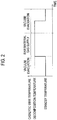
Fig. 2] Fig. 2 is a view for explaining flow of formation of firm according to Example. - Hereinafter, a catalytic CVD equipment will be described with reference to the drawings. It is to be noted that, in the following description of drawings, the same or similar constituent elements are designated by the same or similar reference numerals.
- However, it should be kept in mind that the drawings are schematic, and a rate of each dimension is different from actual one. Therefore, specific dimensions or the like should be determined in consideration of the following description. In addition, it is a matter of course that portions with their different dimensional interrelationships or rates are included in the drawings.
- In the conventional catalytic CVD equipment, a catalytic wire easily breaks, there is a need to frequently replace such a faulty catalytic wire with its replacement wire; and therefore, there has been a problem that manufacturability is degraded.
- Accordingly, the present inventors made their utmost efforts in study with respect to why the catalytic wire easily breaks. As a result, it was determined that there had been a problem in that power supply to the catalytic wire is stopped after the completion of formation of film and then power supply to the catalytic wire is started again at the time of start of formation of film.
- Specifically, when power supply to the catalytic wire has been stopped after the completion of formation of film, a temperature of the catalytic wire lowers from a temperature when the film is formed (for example, 1,600 degrees Centigrade to 2,000 degrees Centigrade) to the order of room temperature within several seconds due to a small thermal capacity of the catalytic wire; and therefore, the catalytic wire rapidly shrinks. In addition, when power supply to the catalytic wire has been started, the temperature of the catalytic wire rises from the order of room temperature to the temperature when the film is formed within several seconds; and therefore, the catalytic wire rapidly expands. It was determined that such shrinkage and expansion are repeated every time stop and start of power supply is switched, thereby reducing serviceable life of the catalytic wire.
- The present invention contrives control of power supply to a catalytic wire to thereby realize extended serviceable life of the catalytic wire. Hereinafter, a description will be furnished, focusing on control of power supply to the catalytic wire.
- Hereinafter, a configuration of a catalytic CVD equipment according to the embodiment will be described with reference to the drawings.
Fig. 1 is a schematic diagram showing a configuration of acatalytic CVD equipment 100. - As shown in
Fig. 1 , thecatalytic CVD equipment 100 has a preparation chamber 1, areaction chamber 10, and a takeout chamber (not shown). Asubstrate 300 that is held on asubstrate tray 200 is moved from the preparation chamber 1 to thereaction chamber 10, making it possible to form a deposited film on thesubstrate 300. - It is to be noted that the preparation chamber 1, the
reaction chamber 10, and the takeout chamber are evacuated at a pressure lower than about 1 x 10⁻⁴ Pa at a time other than when the film is formed in a normal operation state. - The preparation chamber 1 is a vacuum chamber for housing the
substrate tray 200, and is constituted to enable evacuation in a vacuumed state. The preparation chamber 1 is provided with aheating mechanism 2 such as a lamp heater or a sheath heater. - The
heating mechanism 2 heats thesubstrate 300 that is held on thesubstrate tray 200. In this manner, the moisture that is adsorbed on thesubstrate tray 200 and thesubstrate 300 is eliminated. - In addition, the preparation chamber 1 is provided with a take-in device and a takeout device, although not shown. The take-in device takes the
substrate tray 200 in the preparation chamber 1. The takeout device takes out thesubstrate tray 200 that is ready for preparation in the preparation chamber 1 to thereaction chamber 10. - The
reaction chamber 10 is a vacuum chamber for housing thesubstrate tray 200. Thereaction chamber 10 is provided with a gas supply pipe 11, agas discharge pipe 12, a plurality ofcatalytic wires 13, amount portion 14, and apower source 15. - The gas supply pipe 11 is a flow path for supplying a raw material gas (such as a mixture gas of SiH4 and H2 or SiH4, for example) into the
reaction chamber 10. - The
gas discharge pipe 12 is a flow path for discharging a raw material gas from the inside of thereaction chamber 10. - The
catalytic wires 13 are heated to thereby decompose the raw material gas to be supplied into thereaction chamber 10. Both ends of thecatalytic wires 13 are mounted to the mountedportion 14, and are disposed perpendicular to a bottom face of thereaction chamber 10. Thecatalytic wires 13 are heated to a temperature at which a raw material gas can be decomposed (hereinafter, referred to as a "decomposition temperature", which is 1,600 degrees Centigrade to 2,000 degrees Centigrade, for example), by means of power supply. The raw material gas is decomposed by means of thecatalytic wires 13, and decomposed species reaches thesubstrate 300, whereby a deposited film (such as a semiconductor film or a SiN film, for example) is formed on thesubstrate 300. - The
catalytic wires 13 can be made of a material such as Ta, Mo, or W-based wires. In addition, thecatalytic wires 13 may have different kinds of layers on surface. According to the invention claimed in claim 1, the wire is a tantalum wire of which a borate layer is formed on surface. Further, the catalytic wires 11 with their diameter of 0.3 mm to 2.0 mm, preferably 0.5 mm to 1.0 mm are employed. - The
power source 15 supplies power to thecatalytic wires 13 via themount portion 14. As thepower source 15, there can be employed a constant current/constant voltage power supply that is capable of constant current power supply, constant voltage power supply or both of constant current power supply and constant power control. - In the embodiment, control of the
power supply 15 may be either one of constant current control and constant power control, and a temperature of thecatalytic wires 13 is controlled by setting a current value or a power value. That is, the current value or power value of thepower source 15 is controlled so that a current flows into thecatalytic wires 13 to an extent such that the temperature of thecatalytic wires 13 is set at a predetermined temperature. - In addition, the
reaction chamber 10 is provided with a take-in device and a takeout device, although not shown. In this manner, thesubstrate tray 200 is taken in thereaction chamber 10 or is taken out from thereaction chamber 10. - The
catalytic CVD equipment 100 has a control unit, although not shown. - The control unit always continuously supplies power to the
catalytic wires 13 at the time of continuous operation of thecatalytic CVD equipment 100. - Specifically, during a time period during which formation of film is to be performed on the
substrate 300 in the reaction chamber 10 (hereinafter, referred to as "a time period when a film is formed"), the control unit power-supplies a current at which a temperature of thecatalytic wires 13 can be heated to a decomposition temperature of a raw material gas. In addition, during a time period during which formation of film is not performed on thesubstrate 300 in the reaction chamber 10 (hereinafter, referred to as "a time period when no film is formed"), the control unit power-supplies a current at which the temperature of thecatalytic wires 13 can be controlled to a temperature which is lower than the temperature of thecatalytic wires 13 when the film is formed, and is higher than room temperature. In this way, power is continuously supplied to thecatalytic wires 13 when thesubstrate tray 200 is not housed in thereaction chamber 10 as well. Therefore, thecatalytic wires 13 are always powered from the time when the film is formed over the time when no film is formed. - In addition, it is defined in claim 1 that a temperature of the
catalytic wires 13 when no film is formed (hereinafter, referred to as a "standby temperature") be a temperature which is lower than a temperature of thecatalytic wires 13 when the film is formed, and be a temperature which is lower than a decomposition temperature of a raw material gas. In this manner, thecatalytic wires 13 can be restrained from being always heated to a high temperature, thus making it possible to lessen expansion of thecatalytic wires 13. As a result, extended serviceable life of thecatalytic wires 13 can be realized. - Further, it is defined in claim 1 that a standby temperature be a temperature which is higher than a temperature when power supply to the
catalytic wires 13 has been stopped (the order of room temperature), and be a temperature which is higher than a ductile-brittle transition temperature of thecatalytic wires 13. - The "ductile-brittle transition" used herein denotes a phenomenon in which, in a case where a temperature of the catalytic wires has lowered, a material constituting the catalytic wires becomes significantly vulnerable due to the lowering of the temperature. In addition, the "ductile-brittle transition temperature" used herein denotes a temperature at which an ductile-brittle transition occurs with the catalytic wires or part of these wires. For example, the ductile-brittle transition temperature of tungsten (W), which is well known as a material for the catalytic wires, is 300 degrees Centigrade, and becomes extremely vulnerable if a temperature of less than 300 degrees Centigrade is reached. Therefore, in a case where W is employed for the catalytic wires, the standby temperature is set at a temperature which is higher than 300 degrees Centigrade that is the ductile-brittle transition temperature, thereby making it possible to realize extended serviceable life of the catalytic wires.
- Although an ductile-brittle transition temperature in a case where the
catalytic wires 13 have a laminate structure is not clear, for example, it is experimentally verified that, in catalytic wires employing tantalum having a tantalum borate layer on surface, a standby temperature is set at a temperature exceeding 500 degrees Centigrade to thereby realize extended serviceable life. Therefore, in the case of tantalum having a tantalum borate layer on surface, it is deemed that the ductile-brittle transition temperature is about 500 degrees Centigrade. - In addition, the temperature of the
catalytic wires 13 when the film is formed can be appropriately selected as long as it is a temperature at which a raw material gas can be decomposed (i.e., a decomposition temperature), or alternatively, the temperature may be varied. Similarly, the standby temperature can be appropriately selected at a temperature which is lower than the temperature of thecatalytic wires 13 when the film is formed, and is higher than room temperature, or alternatively, the temperature can be varied. - Next, as one example of a method for formation of film employing the
catalytic CVD equipment 100, a method for forming a semiconductor film will be described with reference to the drawings. - First, the
substrate 300 having a first main face and a second main face that is provided at an opposite side of the first main face is prepared. In the embodiment, thesubstrate 300 is made of a material such as glass. - Next, the
substrate 300 is held on thesubstrate tray 200. - Next, the
substrate tray 200 on which thesubstrate 300 is held is taken in the preparation chamber 1 that is maintained at an atmospheric pressure. - Next, by means of evacuation from a evacuation system, the inside of the preparation chamber 1 is evacuated at a predetermined pressure (1 x 10⁻⁴ Pa or less, for example), and by means of the
heating mechanism 2, thesubstrate 300 and thesubstrate tray 200 are heated to the order of about 150 degrees Centigrade to 200 degrees Centigrade. In this manner, the moisture that is adsorbed to thesubstrate 300 and thesubstrate tray 200 is eliminated. - Next, the
substrate tray 200 on which thesubstrate 300 is held is taken from the preparation chamber 1, and is transferred into thereaction chamber 10. At this time, thecatalytic wires 13 that are disposed in thereaction chamber 10 are preheated at a standby temperature by means of continuous power supply. - Next, a mixture gas of SiH4 and H2 is supplied as a raw material gas from the gas supply pipe 11 into the
reaction chamber 10, and the pressure in thereaction chamber 10 is adjusted to a predetermined value (about 0.5 Pa to 10 Pa, for example). - Next, by increasing the current flowing in the
catalytic wires 13, thecatalytic wires 13 are heated up to a decomposition temperature of a raw material gas. In this manner, the raw material gas is decomposed by means of thecatalytic wires 13, and decomposed species reaches the top of the first main face of thesubstrate 300. In this manner, an amorphous Si film is formed on thesubstrate 300. - Next, the current flowing in the
catalytic wires 13 is reduced, and at the same time, supply of the raw material gas is stopped. In this manner, thecatalytic wires 13 are heated up to a standby temperature by means of continuous power supply. - Next, after the pressure in the
reaction chamber 10 has been set at about 1 x 10⁻⁴ or less by means of evacuation from thegas discharge pipe 12, thesubstrate tray 200 on which thesubstrate 300 is held is taken out to the takeout chamber and then is exposed in atmosphere. - While, in the embodiment, the current flowing in the
catalytic wires 13 is reduced, and at the same time, supply of the raw material gas is stopped, the supply of the raw material gas may be stopped after the current has been reduced, or alternatively, the current may be reduced after the supply of the raw material gas has been stopped. - Next, a
substrate tray 200 on which a newlyprepared substrate 300 is held is taken from the preparation chamber 1 and then is transferred into thereaction chamber 10. At this time, thecatalytic wires 13 are maintained at a standby temperature by means of continuous power supply. - Next, the abovementioned raw material gas is supplied from the gas supply pipe 11 into the
reaction chamber 10, whereby the pressure in thereaction chamber 10 is adjusted to a predetermined value (about 0.5 Pa to 10 Pa, for example). - Next, by increasing the current flowing in the
catalytic wire 13, thecatalytic wires 13 are heated up to the decomposition temperature of the raw material gas. In this manner, the raw material gas is decomposed by means of thecatalytic wires 13, and decomposed species reaches the top of thesubstrate 300. - As described above, in a case where formation of film on the
substrate 300 is continuously performed, in the embodiment, the temperature of thecatalytic wires 13 is controlled to a standby temperature which lower than the temperature of thecatalytic wires 13 when the film is formed and is higher than room temperature before and after the film is formed on thesubstrate 300. - In the
catalytic CVD equipment 100 according to the embodiment, the control unit controls a temperature of thecatalytic wires 13 to a standby temperature during predetermined time periods before and after the film is formed. The standby time is a predetermined temperature which is lower than the temperature of thecatalytic wires 13 when the film is formed, and is higher than room temperature. - Therefore, shrinkage and expansion that occur with the
catalytic wires 13 can be mitigated in comparison with a case in which start and stop of power supply by means of thepower source 15 is repeated. Thus, extended serviceable life of thecatalytic wires 13 can be realized. - In addition, the standby temperature is lower than the temperature of the
catalytic wires 13 when the film is formed. Therefore, thecatalytic wires 13 are always maintained at a high temperature, whereby the catalytic wires can be restrained from being maintained in its expanded state. - Further, the
catalytic wires 13 are not always set at a decomposition temperature, thus making it possible to restrain thesubstrate 300 from being overheated. As a result, the quality of film that is formed on thesubstrate 300 can be restrained from being degraded. - Furthermore, it is defined in claim 1 that the standby temperature be higher than the ductile-brittle transition temperature of the
catalytic wires 13. In this case, the fact that the ductile-brittle transition temperature occurs with thecatalytic wires 13 can be restrained, thus making it possible to realize extended serviceable life of thecatalytic wires 13. - Still furthermore, it is preferable that the standby temperature be a temperature at which a temperature of the
substrate 300 can be maintained to be lower than a temperature at which film quality of a film such as an amorphous semiconductor film or a finely crystalline semiconductor film formed on thesubstrate 300 varies. In this case, variation of the film quality can be restrained in the case where the film such as the amorphous semiconductor film or the finely crystalline semiconductor film has been formed on thesubstrate 300 as well. - Yet furthermore, power is continuously supplied to the
catalytic wires 13 at predetermined time intervals before and after the film is formed, whereby thecatalytic wires 13 can be controlled at a predetermined temperature without a need to employ another heating mechanism such as a heater. As a result, reduction of equipment costs can be realized. - Moreover, in the method for formation of film according to the embodiment, the abovementioned
catalytic CVD equipment 100 is employed, thus making it possible to lessen replacement frequency of thecatalytic wires 13. As a result, manufacturability of films can be improved. - In the foregoing embodiment, for example, while a method for forming an amorphous Si film was described as one example of the method for formation of film to which the present invention is applied, the present invention is not limitative thereto. The present invention is also applicable to a method for forming a semiconductor film other than the amorphous Si film or a film other than a semiconductor film such as a SiN film. Further, the present invention is also applicable to a method for manufacturing semiconductor devices such as solar cells which are provided with at least one of a semiconductor film and films other than the semiconductor films.
- In addition, while, in the foregoing embodiment, the
catalytic CVD equipment 100 was arranged to be provided with only onereaction chamber 10, the present invention is not limitative thereto. Thecatalytic CVD equipment 100 may be provided with a plurality of reaction chambers. In this manner, films of a same kind or different kinds can be formed to be superimposed on thesubstrate 300. In a case where a film is further formed on a film that is formed on thesubstrate 300, it is preferable that the standby temperature be a temperature at which the temperature of thesubstrate 300 can be maintained to be lower than a temperature at which the quality of film that is formed on thesubstrate 300 varies. For example, in a case where an amorphous semiconductor film or a finely crystalline semiconductor film has been formed on thesubstrate 300, the standby temperature is controlled to a temperature at which the temperature of thesubstrate 300 can be maintained at about 300 degrees Centigrade or less, thereby making it possible to restrain variation of film quality due to elimination of hydrogen or the like. - First, a tantalum wire whose surface had been borated was disposed as a catalytic wire in a reaction chamber.
- Next, heating and cooling of the catalytic wire were repeatedly performed in accordance with the flowchart shown in
Fig. 2 . - Specifically in the step of vacuum-evacuating the inside of the reaction chamber in advance, a temperature of the catalytic wire was first maintained at a standby temperature (500 degrees Centigrade to 700 degrees Centigrade).
- Next, the temperature of the catalytic wire was maintained at a decomposition temperature (1,600 degrees Centigrade to 2,000 degrees Centigrade) from the step of supplying a raw material gas into the reaction chamber up to partway of the step of vacuum-evacuating the raw material gas from the inside of the reaction chamber.
- Next, the temperature of the catalytic wire was maintained at the standby temperature by continuously supplying power to the catalytic wire from partway of the step of vacuum-evacuating the raw material gas.
- Then, the above steps were repeatedly performed until the catalytic wire had broken.
- In Comparative Example, no power was supplied to the catalytic wire from the step of vacuum-evacuating the inside of the reaction chamber in advance and partway of the step of vacuum-evacuating a raw material gas. Everything else was performed in the same manner as that in Example.
- In Example, serviceable life of the catalytic wire could be increased to be twice or more in comparison with that in Comparative Example. A reason why such a result was obtained is that power was continuously supplied to the catalytic wire in Example, and expansion and shrinkage of the catalytic wire could be mitigated.
- As described above, a catalytic CVD equipment is useful in the field of manufacturing catalytic CVD equipments, since extended serviceable life of catalytic wires can be realized. In addition, a method for formation of film and a process for production of solar cell, are useful in the field of manufacturing solar cells, since manufacturability can be improved.
-
- 1
- Preparation chamber
- 2
- Heating mechanism
- 10
- Reaction chamber
- 11
- Gas supply pipe
- 12
- Gas discharge pipe
- 13
- Catalytic wire
- 14
- Mount portion
- 15
- Power source
- 100
- Catalytic CVD equipment
- 200
- Substrate tray
- 300
- Substrate
Claims (4)
- A method of forming a film on a substrate (300) using a catalytic CVD equipment (100), the catalytic CVD equipment (100) comprising:a reaction chamber (10);a catalytic wire (13) installed in the reaction chamber (10);a power source (15) for supplying power to the catalytic wire (13) to heat the catalytic wire (13); anda control unit for controlling a temperature of the catalytic wire (13) by controlling power-supply from the power source (15) to the catalytic wire (13),wherein the method comprises:supplying a raw material gas to the catalytic wire (13) in the reaction chamber (10);with the control unit, performing a film formation control by controlling the power-supply from the power source (15) to the catalytic wire (13) so that the temperature of the catalytic wire (13) is maintained at a decomposition temperature of the raw material gas, at a time at which formation of the film is to be performed onto the substrate (300) in the reaction chamber (10) by depositing generated decomposed species on the substrate (300), andwith the control unit, continuously before and after the film formation control, performing a no film formation control for controlling the power-supply from the power source (15) to the catalytic wire (13) so that the temperature of the catalytic wire (13) is maintained at a standby temperature which is lower than the decomposition temperature of the raw material gas and higher than a ductile-brittle transition temperature of the catalytic wire (13),characterized in that:the catalytic wire (13) comprises tantalum having a tantalum borate layer on a surface thereof; andthe no film formation control is performed using 500 degrees Centigrade as the ductile-brittle temperature.
- The method according to claim 1, wherein:
the method comprises performing the film formation control and the no film formation control using a value between 1,600 degrees Centigrade and 2,000 degrees Centigrade as the decomposition temperature. - The method according to claim 1 or 2, wherein:
in a case where a second film is formed on a first film formed on a substrate (300) in the reaction chamber (10), the method comprises performing the no film formation control so that the standby temperature is maintained at a temperature lower than a temperature at which the film quality of the first film formed on the substrate (300) varies. - The method according to claim 3, wherein:the first film is an amorphous semiconductor film or a finely crystalline semiconductor film; andwhen forming the second film, the method comprises performing the no film formation control so that a temperature of the substrate (300) is maintained at a temperature lower than 300 degrees Centigrade.
Applications Claiming Priority (2)
| Application Number | Priority Date | Filing Date | Title |
|---|---|---|---|
| JP2009230598A JP5586199B2 (en) | 2009-10-02 | 2009-10-02 | Catalytic CVD apparatus, film forming method, and solar cell manufacturing method |
| PCT/JP2010/067286 WO2011040611A1 (en) | 2009-10-02 | 2010-10-01 | Catalytic cvd device, film forming method and solar cell manufacturing method |
Publications (3)
| Publication Number | Publication Date |
|---|---|
| EP2485248A1 EP2485248A1 (en) | 2012-08-08 |
| EP2485248A4 EP2485248A4 (en) | 2017-01-11 |
| EP2485248B1 true EP2485248B1 (en) | 2020-03-18 |
Family
ID=43826414
Family Applications (1)
| Application Number | Title | Priority Date | Filing Date |
|---|---|---|---|
| EP10820725.9A Active EP2485248B1 (en) | 2009-10-02 | 2010-10-01 | Film forming method using catalytic cvd device |
Country Status (6)
| Country | Link |
|---|---|
| US (1) | US20120190176A1 (en) |
| EP (1) | EP2485248B1 (en) |
| JP (1) | JP5586199B2 (en) |
| KR (1) | KR101603818B1 (en) |
| CN (1) | CN102576668B (en) |
| WO (1) | WO2011040611A1 (en) |
Citations (1)
| Publication number | Priority date | Publication date | Assignee | Title |
|---|---|---|---|---|
| US20050268852A1 (en) * | 2004-05-21 | 2005-12-08 | Masanobu Hatanaka | Vaccum film-forming apparatus |
Family Cites Families (19)
| Publication number | Priority date | Publication date | Assignee | Title |
|---|---|---|---|---|
| US2678870A (en) * | 1950-06-21 | 1954-05-18 | Walter M Weil | Manufacture of refractory metal borides |
| US3024176A (en) * | 1959-08-04 | 1962-03-06 | Gen Electric | Corrosion resistant coating |
| US3650846A (en) * | 1968-11-04 | 1972-03-21 | Gen Electric | Process for reconstituting the grain structure of metal surfaces |
| RU2180771C2 (en) * | 1996-03-12 | 2002-03-20 | Рейкем Корпорейшн | Electric heating system |
| US6468694B1 (en) * | 1997-03-27 | 2002-10-22 | Millennium Cell, Inc. | High energy density boride batteries |
| US20030164225A1 (en) * | 1998-04-20 | 2003-09-04 | Tadashi Sawayama | Processing apparatus, exhaust processing process and plasma processing |
| JP2000183358A (en) * | 1998-07-17 | 2000-06-30 | Sony Corp | Method for manufacturing thin film semiconductor device |
| TWI313059B (en) * | 2000-12-08 | 2009-08-01 | Sony Corporatio | |
| GB2385864A (en) * | 2002-02-28 | 2003-09-03 | Qinetiq Ltd | Production of nanocarbons |
| JP2003303780A (en) * | 2002-04-11 | 2003-10-24 | Ulvac Japan Ltd | Method for controlling catalyst temperature |
| EP1699121B1 (en) * | 2003-12-15 | 2014-04-30 | The Furukawa Electric Co., Ltd. | Semiconductor device manufacturing method |
| TW200533780A (en) * | 2004-03-10 | 2005-10-16 | Ulvac Inc | Self-cleaning catalyst chemical vapor deposition device and cleaning method therefor |
| JP4404674B2 (en) * | 2004-04-07 | 2010-01-27 | 株式会社アルバック | Thin film manufacturing equipment |
| JP4374278B2 (en) | 2004-05-17 | 2009-12-02 | 株式会社アルバック | Catalytic CVD equipment |
| KR100688838B1 (en) * | 2005-05-13 | 2007-03-02 | 삼성에스디아이 주식회사 | Catalytic Chemical Vapor Deposition Apparatus and Catalytic Chemical Vapor Deposition Method |
| JP4818082B2 (en) * | 2006-11-30 | 2011-11-16 | 三洋電機株式会社 | Cat-CVD apparatus and filament exchange method |
| JP4308281B2 (en) * | 2007-04-23 | 2009-08-05 | 三洋電機株式会社 | Photovoltaic element manufacturing method |
| JP2009230598A (en) | 2008-03-25 | 2009-10-08 | Seiko Epson Corp | Image determination device, image determination method, and image determination program |
| RU2486283C2 (en) * | 2008-12-09 | 2013-06-27 | Улвак, Инк. | Apparatus for catalytic chemical vapour deposition |
-
2009
- 2009-10-02 JP JP2009230598A patent/JP5586199B2/en active Active
-
2010
- 2010-10-01 WO PCT/JP2010/067286 patent/WO2011040611A1/en not_active Ceased
- 2010-10-01 EP EP10820725.9A patent/EP2485248B1/en active Active
- 2010-10-01 CN CN201080045522.3A patent/CN102576668B/en active Active
- 2010-10-01 KR KR1020127011214A patent/KR101603818B1/en active Active
-
2012
- 2012-03-30 US US13/436,202 patent/US20120190176A1/en not_active Abandoned
Patent Citations (1)
| Publication number | Priority date | Publication date | Assignee | Title |
|---|---|---|---|---|
| US20050268852A1 (en) * | 2004-05-21 | 2005-12-08 | Masanobu Hatanaka | Vaccum film-forming apparatus |
Also Published As
| Publication number | Publication date |
|---|---|
| JP2011082198A (en) | 2011-04-21 |
| KR20120062924A (en) | 2012-06-14 |
| KR101603818B1 (en) | 2016-03-16 |
| WO2011040611A1 (en) | 2011-04-07 |
| CN102576668B (en) | 2015-07-08 |
| US20120190176A1 (en) | 2012-07-26 |
| EP2485248A1 (en) | 2012-08-08 |
| CN102576668A (en) | 2012-07-11 |
| EP2485248A4 (en) | 2017-01-11 |
| JP5586199B2 (en) | 2014-09-10 |
Similar Documents
| Publication | Publication Date | Title |
|---|---|---|
| KR101976559B1 (en) | Methods for cleaning a surface of a substrate using a hot wire chemical vapor deposition (hwcvd) chamber | |
| KR101132231B1 (en) | Substrate processing apparatus | |
| US20170309490A1 (en) | Method of manufacturing semiconductor device | |
| US20090277386A1 (en) | Catalytic chemical vapor deposition apparatus | |
| EP1258914B1 (en) | Heating element cvd device | |
| JP4601954B2 (en) | Method for manufacturing a coated substrate | |
| JP6336866B2 (en) | Semiconductor device manufacturing method, substrate processing apparatus, and program | |
| US4830891A (en) | Method for selective deposition of metal thin film | |
| US20050115504A1 (en) | Method and apparatus for forming thin films, method for manufacturing solar cell, and solar cell | |
| US7128788B2 (en) | Manufacturing apparatus for buried insulating layer-type semiconductor silicon carbide substrate | |
| TW201122151A (en) | Hot wire chemical vapor deposition (CVD) inline coating tool | |
| US10000850B2 (en) | Deposition method and method of manufacturing a catalyst wire for a catalytic chemical vapor deposition apparatus | |
| US20060216514A1 (en) | Diamond film-forming silicon and its manufacturing method | |
| US20130040414A1 (en) | Method for manufacturing a thin-film solar cell | |
| WO2012117888A1 (en) | Catalytic chemical vapor deposition device, and deposition method and catalyst body surface treatment method using same | |
| WO2012026241A1 (en) | Method for manufacturing semiconductor device, and substrate treatment device | |
| JP2013207057A (en) | Substrate processing apparatus, substrate manufacturing method, and substrate processing apparatus cleaning method | |
| CN1503857A (en) | Method and apparatus for depositing an at least partially crystalline silicon layer on a substrate | |
| EP2485248A1 (en) | Catalytic cvd device, film forming method and solar cell manufacturing method | |
| EP2208806A1 (en) | Heating element CVD system | |
| JP2012134332A (en) | Substrate processing method and substrate processing apparatus | |
| US20030131795A1 (en) | Heating element CVD system and heating element CVD method using the same | |
| JP5357690B2 (en) | Film forming method, solar cell manufacturing method, and catalytic CVD apparatus | |
| JP4217522B2 (en) | Diamond film-forming silicon and manufacturing method thereof | |
| JP2003218046A (en) | Heating element cvd apparatus and heating element cvd method using the same |
Legal Events
| Date | Code | Title | Description |
|---|---|---|---|
| PUAI | Public reference made under article 153(3) epc to a published international application that has entered the european phase |
Free format text: ORIGINAL CODE: 0009012 |
|
| 17P | Request for examination filed |
Effective date: 20120330 |
|
| AK | Designated contracting states |
Kind code of ref document: A1 Designated state(s): AL AT BE BG CH CY CZ DE DK EE ES FI FR GB GR HR HU IE IS IT LI LT LU LV MC MK MT NL NO PL PT RO RS SE SI SK SM TR |
|
| DAX | Request for extension of the european patent (deleted) | ||
| REG | Reference to a national code |
Ref country code: DE Ref legal event code: R079 Ref document number: 602010063574 Country of ref document: DE Free format text: PREVIOUS MAIN CLASS: H01L0021205000 Ipc: C23C0016440000 |
|
| RA4 | Supplementary search report drawn up and despatched (corrected) |
Effective date: 20161209 |
|
| RIC1 | Information provided on ipc code assigned before grant |
Ipc: C23C 16/44 20060101AFI20161205BHEP Ipc: C23C 16/24 20060101ALI20161205BHEP |
|
| STAA | Information on the status of an ep patent application or granted ep patent |
Free format text: STATUS: EXAMINATION IS IN PROGRESS |
|
| 17Q | First examination report despatched |
Effective date: 20180306 |
|
| GRAP | Despatch of communication of intention to grant a patent |
Free format text: ORIGINAL CODE: EPIDOSNIGR1 |
|
| STAA | Information on the status of an ep patent application or granted ep patent |
Free format text: STATUS: GRANT OF PATENT IS INTENDED |
|
| INTG | Intention to grant announced |
Effective date: 20191104 |
|
| GRAS | Grant fee paid |
Free format text: ORIGINAL CODE: EPIDOSNIGR3 |
|
| GRAA | (expected) grant |
Free format text: ORIGINAL CODE: 0009210 |
|
| STAA | Information on the status of an ep patent application or granted ep patent |
Free format text: STATUS: THE PATENT HAS BEEN GRANTED |
|
| AK | Designated contracting states |
Kind code of ref document: B1 Designated state(s): AL AT BE BG CH CY CZ DE DK EE ES FI FR GB GR HR HU IE IS IT LI LT LU LV MC MK MT NL NO PL PT RO RS SE SI SK SM TR |
|
| REG | Reference to a national code |
Ref country code: GB Ref legal event code: FG4D |
|
| REG | Reference to a national code |
Ref country code: DE Ref legal event code: R096 Ref document number: 602010063574 Country of ref document: DE |
|
| REG | Reference to a national code |
Ref country code: AT Ref legal event code: REF Ref document number: 1245994 Country of ref document: AT Kind code of ref document: T Effective date: 20200415 Ref country code: IE Ref legal event code: FG4D |
|
| PG25 | Lapsed in a contracting state [announced via postgrant information from national office to epo] |
Ref country code: NO Free format text: LAPSE BECAUSE OF FAILURE TO SUBMIT A TRANSLATION OF THE DESCRIPTION OR TO PAY THE FEE WITHIN THE PRESCRIBED TIME-LIMIT Effective date: 20200618 Ref country code: FI Free format text: LAPSE BECAUSE OF FAILURE TO SUBMIT A TRANSLATION OF THE DESCRIPTION OR TO PAY THE FEE WITHIN THE PRESCRIBED TIME-LIMIT Effective date: 20200318 Ref country code: RS Free format text: LAPSE BECAUSE OF FAILURE TO SUBMIT A TRANSLATION OF THE DESCRIPTION OR TO PAY THE FEE WITHIN THE PRESCRIBED TIME-LIMIT Effective date: 20200318 |
|
| REG | Reference to a national code |
Ref country code: NL Ref legal event code: MP Effective date: 20200318 |
|
| PG25 | Lapsed in a contracting state [announced via postgrant information from national office to epo] |
Ref country code: BG Free format text: LAPSE BECAUSE OF FAILURE TO SUBMIT A TRANSLATION OF THE DESCRIPTION OR TO PAY THE FEE WITHIN THE PRESCRIBED TIME-LIMIT Effective date: 20200618 Ref country code: GR Free format text: LAPSE BECAUSE OF FAILURE TO SUBMIT A TRANSLATION OF THE DESCRIPTION OR TO PAY THE FEE WITHIN THE PRESCRIBED TIME-LIMIT Effective date: 20200619 Ref country code: HR Free format text: LAPSE BECAUSE OF FAILURE TO SUBMIT A TRANSLATION OF THE DESCRIPTION OR TO PAY THE FEE WITHIN THE PRESCRIBED TIME-LIMIT Effective date: 20200318 Ref country code: LV Free format text: LAPSE BECAUSE OF FAILURE TO SUBMIT A TRANSLATION OF THE DESCRIPTION OR TO PAY THE FEE WITHIN THE PRESCRIBED TIME-LIMIT Effective date: 20200318 Ref country code: SE Free format text: LAPSE BECAUSE OF FAILURE TO SUBMIT A TRANSLATION OF THE DESCRIPTION OR TO PAY THE FEE WITHIN THE PRESCRIBED TIME-LIMIT Effective date: 20200318 |
|
| REG | Reference to a national code |
Ref country code: LT Ref legal event code: MG4D |
|
| PG25 | Lapsed in a contracting state [announced via postgrant information from national office to epo] |
Ref country code: NL Free format text: LAPSE BECAUSE OF FAILURE TO SUBMIT A TRANSLATION OF THE DESCRIPTION OR TO PAY THE FEE WITHIN THE PRESCRIBED TIME-LIMIT Effective date: 20200318 |
|
| PG25 | Lapsed in a contracting state [announced via postgrant information from national office to epo] |
Ref country code: PT Free format text: LAPSE BECAUSE OF FAILURE TO SUBMIT A TRANSLATION OF THE DESCRIPTION OR TO PAY THE FEE WITHIN THE PRESCRIBED TIME-LIMIT Effective date: 20200812 Ref country code: LT Free format text: LAPSE BECAUSE OF FAILURE TO SUBMIT A TRANSLATION OF THE DESCRIPTION OR TO PAY THE FEE WITHIN THE PRESCRIBED TIME-LIMIT Effective date: 20200318 Ref country code: RO Free format text: LAPSE BECAUSE OF FAILURE TO SUBMIT A TRANSLATION OF THE DESCRIPTION OR TO PAY THE FEE WITHIN THE PRESCRIBED TIME-LIMIT Effective date: 20200318 Ref country code: CZ Free format text: LAPSE BECAUSE OF FAILURE TO SUBMIT A TRANSLATION OF THE DESCRIPTION OR TO PAY THE FEE WITHIN THE PRESCRIBED TIME-LIMIT Effective date: 20200318 Ref country code: SK Free format text: LAPSE BECAUSE OF FAILURE TO SUBMIT A TRANSLATION OF THE DESCRIPTION OR TO PAY THE FEE WITHIN THE PRESCRIBED TIME-LIMIT Effective date: 20200318 Ref country code: EE Free format text: LAPSE BECAUSE OF FAILURE TO SUBMIT A TRANSLATION OF THE DESCRIPTION OR TO PAY THE FEE WITHIN THE PRESCRIBED TIME-LIMIT Effective date: 20200318 Ref country code: SM Free format text: LAPSE BECAUSE OF FAILURE TO SUBMIT A TRANSLATION OF THE DESCRIPTION OR TO PAY THE FEE WITHIN THE PRESCRIBED TIME-LIMIT Effective date: 20200318 Ref country code: IS Free format text: LAPSE BECAUSE OF FAILURE TO SUBMIT A TRANSLATION OF THE DESCRIPTION OR TO PAY THE FEE WITHIN THE PRESCRIBED TIME-LIMIT Effective date: 20200718 |
|
| REG | Reference to a national code |
Ref country code: AT Ref legal event code: MK05 Ref document number: 1245994 Country of ref document: AT Kind code of ref document: T Effective date: 20200318 |
|
| REG | Reference to a national code |
Ref country code: DE Ref legal event code: R097 Ref document number: 602010063574 Country of ref document: DE |
|
| PLBE | No opposition filed within time limit |
Free format text: ORIGINAL CODE: 0009261 |
|
| STAA | Information on the status of an ep patent application or granted ep patent |
Free format text: STATUS: NO OPPOSITION FILED WITHIN TIME LIMIT |
|
| PG25 | Lapsed in a contracting state [announced via postgrant information from national office to epo] |
Ref country code: IT Free format text: LAPSE BECAUSE OF FAILURE TO SUBMIT A TRANSLATION OF THE DESCRIPTION OR TO PAY THE FEE WITHIN THE PRESCRIBED TIME-LIMIT Effective date: 20200318 Ref country code: ES Free format text: LAPSE BECAUSE OF FAILURE TO SUBMIT A TRANSLATION OF THE DESCRIPTION OR TO PAY THE FEE WITHIN THE PRESCRIBED TIME-LIMIT Effective date: 20200318 Ref country code: AT Free format text: LAPSE BECAUSE OF FAILURE TO SUBMIT A TRANSLATION OF THE DESCRIPTION OR TO PAY THE FEE WITHIN THE PRESCRIBED TIME-LIMIT Effective date: 20200318 Ref country code: DK Free format text: LAPSE BECAUSE OF FAILURE TO SUBMIT A TRANSLATION OF THE DESCRIPTION OR TO PAY THE FEE WITHIN THE PRESCRIBED TIME-LIMIT Effective date: 20200318 |
|
| 26N | No opposition filed |
Effective date: 20201221 |
|
| PG25 | Lapsed in a contracting state [announced via postgrant information from national office to epo] |
Ref country code: PL Free format text: LAPSE BECAUSE OF FAILURE TO SUBMIT A TRANSLATION OF THE DESCRIPTION OR TO PAY THE FEE WITHIN THE PRESCRIBED TIME-LIMIT Effective date: 20200318 |
|
| PG25 | Lapsed in a contracting state [announced via postgrant information from national office to epo] |
Ref country code: SI Free format text: LAPSE BECAUSE OF FAILURE TO SUBMIT A TRANSLATION OF THE DESCRIPTION OR TO PAY THE FEE WITHIN THE PRESCRIBED TIME-LIMIT Effective date: 20200318 |
|
| REG | Reference to a national code |
Ref country code: CH Ref legal event code: PL |
|
| GBPC | Gb: european patent ceased through non-payment of renewal fee |
Effective date: 20201001 |
|
| PG25 | Lapsed in a contracting state [announced via postgrant information from national office to epo] |
Ref country code: LU Free format text: LAPSE BECAUSE OF NON-PAYMENT OF DUE FEES Effective date: 20201001 Ref country code: MC Free format text: LAPSE BECAUSE OF FAILURE TO SUBMIT A TRANSLATION OF THE DESCRIPTION OR TO PAY THE FEE WITHIN THE PRESCRIBED TIME-LIMIT Effective date: 20200318 |
|
| REG | Reference to a national code |
Ref country code: BE Ref legal event code: MM Effective date: 20201031 |
|
| PG25 | Lapsed in a contracting state [announced via postgrant information from national office to epo] |
Ref country code: LI Free format text: LAPSE BECAUSE OF NON-PAYMENT OF DUE FEES Effective date: 20201031 Ref country code: GB Free format text: LAPSE BECAUSE OF NON-PAYMENT OF DUE FEES Effective date: 20201001 Ref country code: BE Free format text: LAPSE BECAUSE OF NON-PAYMENT OF DUE FEES Effective date: 20201031 Ref country code: CH Free format text: LAPSE BECAUSE OF NON-PAYMENT OF DUE FEES Effective date: 20201031 |
|
| PG25 | Lapsed in a contracting state [announced via postgrant information from national office to epo] |
Ref country code: IE Free format text: LAPSE BECAUSE OF NON-PAYMENT OF DUE FEES Effective date: 20201001 |
|
| PG25 | Lapsed in a contracting state [announced via postgrant information from national office to epo] |
Ref country code: TR Free format text: LAPSE BECAUSE OF FAILURE TO SUBMIT A TRANSLATION OF THE DESCRIPTION OR TO PAY THE FEE WITHIN THE PRESCRIBED TIME-LIMIT Effective date: 20200318 Ref country code: MT Free format text: LAPSE BECAUSE OF FAILURE TO SUBMIT A TRANSLATION OF THE DESCRIPTION OR TO PAY THE FEE WITHIN THE PRESCRIBED TIME-LIMIT Effective date: 20200318 Ref country code: CY Free format text: LAPSE BECAUSE OF FAILURE TO SUBMIT A TRANSLATION OF THE DESCRIPTION OR TO PAY THE FEE WITHIN THE PRESCRIBED TIME-LIMIT Effective date: 20200318 |
|
| PG25 | Lapsed in a contracting state [announced via postgrant information from national office to epo] |
Ref country code: MK Free format text: LAPSE BECAUSE OF FAILURE TO SUBMIT A TRANSLATION OF THE DESCRIPTION OR TO PAY THE FEE WITHIN THE PRESCRIBED TIME-LIMIT Effective date: 20200318 Ref country code: AL Free format text: LAPSE BECAUSE OF FAILURE TO SUBMIT A TRANSLATION OF THE DESCRIPTION OR TO PAY THE FEE WITHIN THE PRESCRIBED TIME-LIMIT Effective date: 20200318 |
|
| REG | Reference to a national code |
Ref country code: DE Ref legal event code: R081 Ref document number: 602010063574 Country of ref document: DE Owner name: ULVAC, INC., CHIGASAKI-SHI, JP Free format text: FORMER OWNERS: SANYO ELECTRIC CO., LTD., OSAKA, JP; ULVAC, INC., CHIGASAKI-SHI, KANAGAWA, JP |
|
| PGFP | Annual fee paid to national office [announced via postgrant information from national office to epo] |
Ref country code: FR Payment date: 20250908 Year of fee payment: 16 |
|
| PGFP | Annual fee paid to national office [announced via postgrant information from national office to epo] |
Ref country code: DE Payment date: 20250902 Year of fee payment: 16 |