EP2482313A1 - Semiconductor device and method of manufacturing the same - Google Patents
Semiconductor device and method of manufacturing the same Download PDFInfo
- Publication number
- EP2482313A1 EP2482313A1 EP20110189873 EP11189873A EP2482313A1 EP 2482313 A1 EP2482313 A1 EP 2482313A1 EP 20110189873 EP20110189873 EP 20110189873 EP 11189873 A EP11189873 A EP 11189873A EP 2482313 A1 EP2482313 A1 EP 2482313A1
- Authority
- EP
- European Patent Office
- Prior art keywords
- region
- element isolation
- isolation film
- gate electrode
- semiconductor substrate
- Prior art date
- Legal status (The legal status is an assumption and is not a legal conclusion. Google has not performed a legal analysis and makes no representation as to the accuracy of the status listed.)
- Ceased
Links
Images









Classifications
-
- H—ELECTRICITY
- H10—SEMICONDUCTOR DEVICES; ELECTRIC SOLID-STATE DEVICES NOT OTHERWISE PROVIDED FOR
- H10D—INORGANIC ELECTRIC SEMICONDUCTOR DEVICES
- H10D89/00—Aspects of integrated devices not covered by groups H10D84/00 - H10D88/00
- H10D89/60—Integrated devices comprising arrangements for electrical or thermal protection, e.g. protection circuits against electrostatic discharge [ESD]
- H10D89/601—Integrated devices comprising arrangements for electrical or thermal protection, e.g. protection circuits against electrostatic discharge [ESD] for devices having insulated gate electrodes, e.g. for IGFETs or IGBTs
- H10D89/711—Integrated devices comprising arrangements for electrical or thermal protection, e.g. protection circuits against electrostatic discharge [ESD] for devices having insulated gate electrodes, e.g. for IGFETs or IGBTs using bipolar transistors as protective elements
- H10D89/713—Integrated devices comprising arrangements for electrical or thermal protection, e.g. protection circuits against electrostatic discharge [ESD] for devices having insulated gate electrodes, e.g. for IGFETs or IGBTs using bipolar transistors as protective elements including a PNP transistor and a NPN transistor, wherein each of said transistors has its base region coupled to the collector region of the other transistor, e.g. silicon controlled rectifier [SCR] devices
-
- H—ELECTRICITY
- H10—SEMICONDUCTOR DEVICES; ELECTRIC SOLID-STATE DEVICES NOT OTHERWISE PROVIDED FOR
- H10D—INORGANIC ELECTRIC SEMICONDUCTOR DEVICES
- H10D89/00—Aspects of integrated devices not covered by groups H10D84/00 - H10D88/00
- H10D89/60—Integrated devices comprising arrangements for electrical or thermal protection, e.g. protection circuits against electrostatic discharge [ESD]
- H10D89/601—Integrated devices comprising arrangements for electrical or thermal protection, e.g. protection circuits against electrostatic discharge [ESD] for devices having insulated gate electrodes, e.g. for IGFETs or IGBTs
- H10D89/811—Integrated devices comprising arrangements for electrical or thermal protection, e.g. protection circuits against electrostatic discharge [ESD] for devices having insulated gate electrodes, e.g. for IGFETs or IGBTs using FETs as protective elements
- H10D89/813—Integrated devices comprising arrangements for electrical or thermal protection, e.g. protection circuits against electrostatic discharge [ESD] for devices having insulated gate electrodes, e.g. for IGFETs or IGBTs using FETs as protective elements specially adapted to provide an electrical current path other than the field-effect induced current path
- H10D89/815—Integrated devices comprising arrangements for electrical or thermal protection, e.g. protection circuits against electrostatic discharge [ESD] for devices having insulated gate electrodes, e.g. for IGFETs or IGBTs using FETs as protective elements specially adapted to provide an electrical current path other than the field-effect induced current path involving a parasitic bipolar transistor triggered by the local electrical biasing of the layer acting as base region of said parasitic bipolar transistor
-
- H—ELECTRICITY
- H10—SEMICONDUCTOR DEVICES; ELECTRIC SOLID-STATE DEVICES NOT OTHERWISE PROVIDED FOR
- H10D—INORGANIC ELECTRIC SEMICONDUCTOR DEVICES
- H10D18/00—Thyristors
- H10D18/01—Manufacture or treatment
- H10D18/031—Manufacture or treatment of lateral or planar thyristors
-
- H—ELECTRICITY
- H10—SEMICONDUCTOR DEVICES; ELECTRIC SOLID-STATE DEVICES NOT OTHERWISE PROVIDED FOR
- H10D—INORGANIC ELECTRIC SEMICONDUCTOR DEVICES
- H10D18/00—Thyristors
- H10D18/251—Lateral thyristors
-
- H—ELECTRICITY
- H10—SEMICONDUCTOR DEVICES; ELECTRIC SOLID-STATE DEVICES NOT OTHERWISE PROVIDED FOR
- H10D—INORGANIC ELECTRIC SEMICONDUCTOR DEVICES
- H10D30/00—Field-effect transistors [FET]
- H10D30/01—Manufacture or treatment
- H10D30/021—Manufacture or treatment of FETs having insulated gates [IGFET]
- H10D30/028—Manufacture or treatment of FETs having insulated gates [IGFET] of double-diffused metal oxide semiconductor [DMOS] FETs
- H10D30/0281—Manufacture or treatment of FETs having insulated gates [IGFET] of double-diffused metal oxide semiconductor [DMOS] FETs of lateral DMOS [LDMOS] FETs
- H10D30/0285—Manufacture or treatment of FETs having insulated gates [IGFET] of double-diffused metal oxide semiconductor [DMOS] FETs of lateral DMOS [LDMOS] FETs using formation of insulating sidewall spacers
-
- H—ELECTRICITY
- H10—SEMICONDUCTOR DEVICES; ELECTRIC SOLID-STATE DEVICES NOT OTHERWISE PROVIDED FOR
- H10D—INORGANIC ELECTRIC SEMICONDUCTOR DEVICES
- H10D30/00—Field-effect transistors [FET]
- H10D30/60—Insulated-gate field-effect transistors [IGFET]
- H10D30/64—Double-diffused metal-oxide semiconductor [DMOS] FETs
- H10D30/65—Lateral DMOS [LDMOS] FETs
-
- H—ELECTRICITY
- H10—SEMICONDUCTOR DEVICES; ELECTRIC SOLID-STATE DEVICES NOT OTHERWISE PROVIDED FOR
- H10D—INORGANIC ELECTRIC SEMICONDUCTOR DEVICES
- H10D62/00—Semiconductor bodies, or regions thereof, of devices having potential barriers
- H10D62/10—Shapes, relative sizes or dispositions of the regions of the semiconductor bodies; Shapes of the semiconductor bodies
- H10D62/113—Isolations within a component, i.e. internal isolations
- H10D62/115—Dielectric isolations, e.g. air gaps
-
- H—ELECTRICITY
- H10—SEMICONDUCTOR DEVICES; ELECTRIC SOLID-STATE DEVICES NOT OTHERWISE PROVIDED FOR
- H10D—INORGANIC ELECTRIC SEMICONDUCTOR DEVICES
- H10D62/00—Semiconductor bodies, or regions thereof, of devices having potential barriers
- H10D62/10—Shapes, relative sizes or dispositions of the regions of the semiconductor bodies; Shapes of the semiconductor bodies
- H10D62/113—Isolations within a component, i.e. internal isolations
- H10D62/115—Dielectric isolations, e.g. air gaps
- H10D62/116—Dielectric isolations, e.g. air gaps adjoining the input or output regions of field-effect devices, e.g. adjoining source or drain regions
-
- H—ELECTRICITY
- H10—SEMICONDUCTOR DEVICES; ELECTRIC SOLID-STATE DEVICES NOT OTHERWISE PROVIDED FOR
- H10D—INORGANIC ELECTRIC SEMICONDUCTOR DEVICES
- H10D62/00—Semiconductor bodies, or regions thereof, of devices having potential barriers
- H10D62/10—Shapes, relative sizes or dispositions of the regions of the semiconductor bodies; Shapes of the semiconductor bodies
- H10D62/124—Shapes, relative sizes or dispositions of the regions of semiconductor bodies or of junctions between the regions
- H10D62/126—Top-view geometrical layouts of the regions or the junctions
- H10D62/127—Top-view geometrical layouts of the regions or the junctions of cellular field-effect devices, e.g. multicellular DMOS transistors or IGBTs
-
- H—ELECTRICITY
- H10—SEMICONDUCTOR DEVICES; ELECTRIC SOLID-STATE DEVICES NOT OTHERWISE PROVIDED FOR
- H10D—INORGANIC ELECTRIC SEMICONDUCTOR DEVICES
- H10D62/00—Semiconductor bodies, or regions thereof, of devices having potential barriers
- H10D62/80—Semiconductor bodies, or regions thereof, of devices having potential barriers characterised by the materials
- H10D62/83—Semiconductor bodies, or regions thereof, of devices having potential barriers characterised by the materials being Group IV materials, e.g. B-doped Si or undoped Ge
-
- H—ELECTRICITY
- H10—SEMICONDUCTOR DEVICES; ELECTRIC SOLID-STATE DEVICES NOT OTHERWISE PROVIDED FOR
- H10D—INORGANIC ELECTRIC SEMICONDUCTOR DEVICES
- H10D64/00—Electrodes of devices having potential barriers
- H10D64/111—Field plates
-
- H—ELECTRICITY
- H10—SEMICONDUCTOR DEVICES; ELECTRIC SOLID-STATE DEVICES NOT OTHERWISE PROVIDED FOR
- H10D—INORGANIC ELECTRIC SEMICONDUCTOR DEVICES
- H10D64/00—Electrodes of devices having potential barriers
- H10D64/20—Electrodes characterised by their shapes, relative sizes or dispositions
- H10D64/27—Electrodes not carrying the current to be rectified, amplified, oscillated or switched, e.g. gates
- H10D64/311—Gate electrodes for field-effect devices
- H10D64/411—Gate electrodes for field-effect devices for FETs
- H10D64/511—Gate electrodes for field-effect devices for FETs for IGFETs
- H10D64/517—Gate electrodes for field-effect devices for FETs for IGFETs characterised by the conducting layers
- H10D64/519—Gate electrodes for field-effect devices for FETs for IGFETs characterised by the conducting layers characterised by their top-view geometrical layouts
-
- H—ELECTRICITY
- H10—SEMICONDUCTOR DEVICES; ELECTRIC SOLID-STATE DEVICES NOT OTHERWISE PROVIDED FOR
- H10D—INORGANIC ELECTRIC SEMICONDUCTOR DEVICES
- H10D64/00—Electrodes of devices having potential barriers
- H10D64/60—Electrodes characterised by their materials
- H10D64/62—Electrodes ohmically coupled to a semiconductor
-
- H—ELECTRICITY
- H10—SEMICONDUCTOR DEVICES; ELECTRIC SOLID-STATE DEVICES NOT OTHERWISE PROVIDED FOR
- H10D—INORGANIC ELECTRIC SEMICONDUCTOR DEVICES
- H10D64/00—Electrodes of devices having potential barriers
- H10D64/60—Electrodes characterised by their materials
- H10D64/66—Electrodes having a conductor capacitively coupled to a semiconductor by an insulator, e.g. MIS electrodes
- H10D64/661—Electrodes having a conductor capacitively coupled to a semiconductor by an insulator, e.g. MIS electrodes the conductor comprising a layer of silicon contacting the insulator, e.g. polysilicon having vertical doping variation
- H10D64/662—Electrodes having a conductor capacitively coupled to a semiconductor by an insulator, e.g. MIS electrodes the conductor comprising a layer of silicon contacting the insulator, e.g. polysilicon having vertical doping variation the conductor further comprising additional layers, e.g. multiple silicon layers having different crystal structures
- H10D64/663—Electrodes having a conductor capacitively coupled to a semiconductor by an insulator, e.g. MIS electrodes the conductor comprising a layer of silicon contacting the insulator, e.g. polysilicon having vertical doping variation the conductor further comprising additional layers, e.g. multiple silicon layers having different crystal structures the additional layers comprising a silicide layer contacting the layer of silicon, e.g. polycide gates
-
- H—ELECTRICITY
- H10—SEMICONDUCTOR DEVICES; ELECTRIC SOLID-STATE DEVICES NOT OTHERWISE PROVIDED FOR
- H10D—INORGANIC ELECTRIC SEMICONDUCTOR DEVICES
- H10D8/00—Diodes
- H10D8/01—Manufacture or treatment
- H10D8/041—Manufacture or treatment of multilayer diodes
-
- H—ELECTRICITY
- H10—SEMICONDUCTOR DEVICES; ELECTRIC SOLID-STATE DEVICES NOT OTHERWISE PROVIDED FOR
- H10D—INORGANIC ELECTRIC SEMICONDUCTOR DEVICES
- H10D8/00—Diodes
- H10D8/80—PNPN diodes, e.g. Shockley diodes or break-over diodes
Definitions
- the embodiments discussed herein relate to a semiconductor device including a laterally diffused metal oxide semiconductor (LDMOS) transistor and an electrostatic discharge (ESD) protection element, and a method of manufacturing the semiconductor device.
- LDMOS laterally diffused metal oxide semiconductor
- ESD electrostatic discharge
- LDMOS transistors are advantageous in that the LDMOS transistors can be fabricated at lower costs than the compound semiconductor elements.
- the LDMOS transistors are also advantageous in that the breakdown voltage thereof can be enhanced relatively easily.
- Semiconductor devices (integrated circuits) each internally including an LDMOS transistor are widely used in mobile phones, wireless LAN equipment, in-vehicle electronic devices, and the like.
- Embodiments of the present invention provide a semiconductor device, and a method of manufacturing the same, the semiconductor device including an LDMOS transistor and an ESD protection element, being producible in simple manufacturing processes and enabling higher integration while ensuring a desired characteristic.
- a semiconductor device including a LDMOS (Laterally Diffused MOS) transistor and an ESD (Electrostatic Discharge) protection element.
- the LDMOS transistor includes: a first gate electrode formed on the semiconductor substrate with an insulating film interposed therebetween; a first body region formed by implanting impurities of a first conductivity type into the semiconductor substrate and disposed at one edge side of the first gate electrode; a first source region of a second conductivity type disposed in an upper portion of the first body region; a first element isolation film formed in an upper portion of the semiconductor substrate and disposed to overlap the first gate electrode; a first drain region formed inside the semiconductor substrate, including impurities of the second conductivity type, and disposed at a position in contact with an edge portion of the first element isolation film and away from the first gate electrode; and a first drift region formed inside the semiconductor substrate, including impurities of the second conductivity type, and being in contact with the first body region and the first drain region.
- the ESD protection element includes: a second gate electrode formed on the semiconductor substrate with an insulating film interposed therebetween; a second body region formed inside the semiconductor substrate, including impurities of the first conductivity type, and disposed at one edge side of the second gate electrode; a second source region of the second conductivity type disposed in an upper portion of the second body region; a second element isolation film formed in an upper portion of the semiconductor substrate and disposed to overlap the second gate electrode; an anode region formed inside the semiconductor substrate, including impurities of the first conductivity type, and disposed at a position in contact with an edge portion of the second element isolation film and away from the second gate electrode; a third element isolation film formed in an upper portion of the semiconductor substrate and disposed adjacent to the anode region; a second drain region formed inside the semiconductor substrate, including impurities of the second conductivity type, and being in contact with the third element isolation film; and a second drift region formed inside the semiconductor substrate, including impurities of the second conductivity type, and being in contact with the second body region, the
- the LDMOS transistor and the ESD protection element may be formed simultaneously, which avoid an increase in the number of manufacturing processes.
- the semiconductor device obtains a desirable characteristic while suppressing an enlargement of an element region.
- higher integration of semiconductor devices may be achieved.
- Fig. 1 is a cross sectional view of a semiconductor device of a first embodiment
- Fig. 2 is a layout of the semiconductor device.
- a first conductivity type is p-type and a second conductivity type is n-type.
- the first conductivity type may be n-type and the second conductivity type may be p-type.
- an element isolation film 11a is formed in a predetermined region of a p-type (first conductivity type) silicon semiconductor substrate 10 and defines an LDMOS transistor formation region (referred to as an LDMOS formation region in the drawings: the same shall apply below) and an ESD protection element formation region.
- An LDMOS transistor is formed in the LDMOS transistor formation region and a thyristor-type ESD protection element is formed in the ESD protection element formation region.
- the LDMOS transistor formation region is surrounded by the element isolation film 11a.
- This LDMOS transistor formation region is provided with a drift region 14a formed by introducing n-type (second conductivity type) impurities into the semiconductor substrate 10.
- an element isolation film 11b traversing the LDMOS transistor formation region is formed in a predetermined region in an upper portion of the semiconductor substrate 10.
- a gate insulating film 17 is formed on the semiconductor substrate 10 to run along almost the center of the LDMOS transistor formation region. A portion (a right side portion in Fig. 1 ) of the gate insulating film 17 is arranged on the element isolation film 11b. A gate electrode 18a traversing the LDMOS transistor formation region and side walls 21 arranged at both sides of the gate electrode 18a in a width direction are formed on the gate insulating film 17. In addition, a silicide film 25b is formed on an upper surface of the gate electrode 18a.
- a body region 16a formed by introducing p-type impurities is arranged at one side of the gate electrode 18a in the width direction (the left side in Figs. 1 and 2 ).
- a source region 19a formed by introducing n-type impurities is arranged in an upper portion of the body region 16a.
- An n-type high concentration impurity region 23a into which n-type impurities are introduced at a higher concentration than in the source region 19a is provide in an upper portion of the source region 19a.
- a p-type high concentration impurity region 22a into which p-type impurities are introduced at a higher concentration than in the body region 16a is provided in an upper portion of the body region 16a between the n-type high concentration impurity region 23a and the element isolation film 11a.
- a silicide film 25a is formed on surfaces of the n-type high concentration impurity region 23a and the p-type high concentration impurity region 22a.
- the n-type high concentration impurity region 23a and the p-type high concentration impurity region 22a are electrically connected to each other through the silicide film 25a.
- the n-type high concentration impurity region 23a and the p-type high concentration impurity region 22a are in contact with each other, but an element isolation film may be formed between these impurity regions 23a, 22a.
- an element isolation film may be formed between these impurity regions 23a, 22a. The same shall apply in other embodiments.
- a drain region 20a formed by introducing n-type impurities is arranged between the element isolation film 11b and the element isolation film 11a on the opposite side in the width direction (the right side in Fig. 1 ).
- An n-type high concentration impurity region 23b into which n-type impurities are introduced at a higher concentration than in the drain region 20a is provided in an upper portion of the drain region 20a and a silicide film 25c is formed on a surface of the n-type high concentration impurity region 23b.
- An interlayer insulating film 27 is formed on top of the semiconductor substrate 10 in the LDMOS transistor formation region, and the gate electrode 18a is covered with the interlayer insulating film 27.
- the silicide films 25a, 25b, 25c are electrically connected to interconnections 28 on the interlayer insulating film 27 through conductive plugs 26a, 26b, 26c, respectively.
- the ESD protection element formation region is also surrounded by the element isolation film 11a.
- the ESD protection element formation region is also provided with a drift region 14b formed by introducing n-type impurities into the semiconductor substrate 10.
- element isolation films 11c, 11d traversing the ESD protection element formation region are formed in predetermined regions in an upper portion of the semiconductor substrate 10.
- the element isolation films 11c, 11d are arranged in parallel with each other.
- a gate insulating film 17 is formed on the semiconductor substrate 10 to traverse the ESD protection element formation region.
- a portion (a right side portion in Fig. 1 ) of the gate insulating film 17 is arranged on the element isolation film 11c.
- a gate electrode 18b traversing the ESD protection element formation region and side walls 21 arranged at both sides of the gate electrode 18b in the width direction are formed on the gate insulating film 17.
- a silicide film 25e is formed on an upper surface of the gate electrode 18b.
- a body region 16b formed by introducing p-type impurities is arranged at one side of the gate electrode 18b in the width direction (the left side in Figs. 1 and 2 ).
- a source region 19b formed by introducing n-type impurities is arranged in an upper portion of the body region 16b.
- An n-type high concentration impurity region 23c into which n-type impurities are introduced at a higher concentration than in the source region 19b is provide in an upper portion of the source region 19b.
- a p-type high concentration impurity region 22b into which p-type impurities are introduced at a higher concentration than in the body region 16b is provided in an upper portion of the body region 16b between the n-type high concentration impurity region 23c and the element isolation film 11a.
- a silicide film 25d is formed on surfaces of the n-type high concentration impurity region 23c and the p-type high concentration impurity region 22b.
- the n-type high concentration impurity region 23c and the p-type high concentration impurity region 22b are electrically connected to each other through the silicide film 25d.
- the n-type high concentration impurity region 23c and the p-type high concentration impurity region 22b are in contact with each other, but an element isolation film may be formed between these impurity regions 23c, 22b.
- an element isolation film may be formed between these impurity regions 23c, 22b. The same shall apply in other embodiments.
- an anode region 22c formed by introducing p-type impurities is formed between the element isolation film 11c and the element isolation film 11d.
- a silicide film 25f is formed on a surface of the anode region 22c.
- a drain region 20b formed by introducing n-type impurities is arranged between the element isolation film 11d and the element isolation film 11a on the opposite side (the right side in Fig. 1 ).
- An n-type high concentration impurity region 23d into which n-type impurities are introduced at a higher concentration than in the drain region 20b is provided in an upper portion of the drain region 20b and a silicide film 25g is formed on a surface of the n-type high concentration impurity region 23d.
- the interlayer insulating film 27 is also formed on top of the semiconductor substrate 10 in the ESD protection element formation region, and the gate electrode 18b is covered with the interlayer insulating film 27.
- the silicide films 25d, 25e, 25f, 25g are electrically connected to interconnections 28 on the interlayer insulating film 27 through conductive plugs 26d, 26e, 26f, 26g, respectively.
- A1 denotes the length of a portion where the element isolation film 11b overlaps the gate electrode 18a above the element isolation film 11b
- B1 denotes a distance between an edge portion of the gate electrode 18a and the drain region 20a (that is, a distance in a direction parallel to the substrate surface).
- A2 denotes a length of a portion where the element isolation film 11c overlaps the gate electrode 18b above the element isolation film 11c
- B2 denotes a distance between an edge portion of the gate electrode 18b and the anode region 22c (that is, a distance in the direction parallel to the substrate surface).
- the ESD protection element with the foregoing structure will be described in more detail.
- the source region 19b, the body region 16b and the gate electrode 18b in the ESD protection element are connected to a single terminal T1.
- the anode region 22c and the drain region 20b are connected to a single terminal T2.
- the terminal T1 is connected to a low potential terminal of an internal circuit (the circuit including the LDMOS transistor), and the terminal T2 is connected to a high potential terminal of the internal circuit, for example.
- Fig. 4 is a diagram explaining an operation of the ESD protection element with a voltage on the horizontal axis and an electric current on the vertical axis.
- an operation voltage in the internal circuit of the semiconductor device (a highest voltage applied between the terminals T1 and T2 in a normal operation) is denoted by V DD
- an operation start voltage of the ESD protection element is denoted by Vt1
- a voltage to break down the internal circuit (hereinafter, referred to as a breakdown voltage)
- V DDMAX a voltage to break down the internal circuit
- the ESD protection element is in an off state when the voltage applied to the internal circuit is lower than the operation start voltage Vt1.
- the ESD protection element When a higher voltage is applied between the terminals T1, T2 due to static electricity or the like, the ESD protection element is turned into an on state and an electric current flows into the ESD protection element. At this time, the electric current flowing through the ESD protection element causes a change in the voltage between the terminals T1, T2.
- V DDMAX breakdown voltage
- the punch-through is a phenomenon in which the depletion layer between the body region 16b and the drift region 14b and the depletion layer between the drift region 14b and the anode region 22c are connected to each other to cause a large electric current to flow.
- One possible method to prevent a punch-through is to make the impurity concentration of the drift region 14b in the ESD protection element formation region higher than the impurity concentration of the drift region 14a in the LDMOS transistor formation region. In this case, however, since a junction breakdown voltage between the body region 16b and the drift region 14b is lowered, the operation start voltage Vt1 of the ESD protection element may become lower than the operation voltage V DD of the LDMOS transistor even though the punch-through is prevented. In addition, there also arises another problem of an increase in the number of manufacturing processes.
- Another possible method to prevent a punch-through is to increase the distance between the body region 16b and the anode region 22c.
- a simple increase in the distance between the body region 16b and the anode region 22c may raise the junction breakdown voltage between the body region 16b and the drift region 14b and thereby make the operation start voltage Vt1 of the ESD protection element higher than the breakdown voltage V DDMAX of the internal circuit.
- this method impedes achievement of higher integration of the semiconductor device.
- the junction breakdown voltage between the body region and the drift region largely depends on the length (overlap length) of the portion where the element isolation film overlaps the gate electrode.
- Fig. 5 is a diagram exemplifying a relationship between a breakdown voltage and the overlap length of the gate electrode and the element isolation film, with the breakdown voltage on the vertical axis and the overlap length on the horizontal axis.
- the junction breakdown voltage between body region 16a or 16b and drift region 14a or 14b depends on the overlap length of the gate electrode 18a or 18b and the element isolation film 11b or 11c. This is because a voltage applied to the gate electrode 18a or 18b largely influences the expansion of the depletion layer in the drift region 14a or 14b.
- the junction breakdown voltage between the drift region 14b and the body region 16b in the ESD protection element becomes higher than the junction breakdown voltage between the drift region 14a and the body region 16a in the LDMOS transistor.
- the operation start voltage Vt1 of the ESD protection element may become higher than the breakdown voltage V DDMAX of the internal circuit, in some cases.
- the junction breakdown voltage between the body region 16b and the drift region 14b in the ESD protection element is made equal to or slightly smaller than the junction breakdown voltage between the body region 16a and the drift region 14a in the LDMOS transistor.
- the distance between the edge portion of the gate electrode 18b and the anode region 22c is increased to prevent the occurrence of a punch-through.
- the increase in the distance between the edge portion of the gate electrode 18b and the anode region 22c may raise the junction breakdown voltage between the body region 16b and the drift region 14b in the ESD protection element in some cases depending on manufacturing conditions. This influence, however, is smaller than in the case where the overlap length of the gate electrode and the element isolation film is changed.
- the distance between the edge portion of the gate electrode 18b and the anode region 22c is increased. This increase more suppresses an enlargement of the ESD protection element formation region than in the case where the distance between the body region and the anode region is simply increased. In this way, the semiconductor device obtains a desirable characteristic while achieving higher integration.
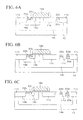
- Fig. 6A is a cross sectional view of the LDMOS transistors of the semiconductor devices in the embodiment and the comparative example
- Fig. 6B is a cross sectional view of the ESD protection element of the semiconductor device in the embodiment
- Fig. 6C is a cross sectional view of the ESD protection element of the semiconductor device in the comparative example.
- the same portions as those in Fig. 1 are indicated by the same reference numerals.
- illustrations of the silicide film, the interlayer insulating film and the like are omitted.
- the ESD protection element of the semiconductor device in the embodiment is simply referred to as the ESD protection element in the embodiment
- the ESD protection element of the semiconductor device in the comparative example is simply referred to as the ESD protection element in the comparative example.
- the ESD protection elements of the semiconductor devices in the embodiment and the comparative example are the same in shape and size.
- the anode region 22c is in contact with the element isolation films 11c, 11d.
- the anode region 22d is away from the element isolation film 11c because the element isolation film 11c has a smaller width.
- the ESD protection element in the embodiment and the ESD protection element in the comparative example are the same in the other portions.
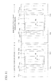
- Fig. 7 is a diagram illustrating simulation results of breakdown voltage characteristics of the ESD protection element in the embodiment and the ESD protection element in the comparative example, with the distance between the gate electrode and the anode region on the horizontal axis and with the breakdown voltage on the vertical axis.
- the overlap length of the gate electrode 18b and the element isolation film 11c is 0.75 ⁇ m in both the ESD protection elements in the embodiment and the comparative example.
- Fig. 7 also illustrates the breakdown voltage characteristic of the LDMOS transistor. In the case of the LDMOS transistor, the horizontal axis indicates the distance between the gate electrode and the drain region.
- the ESD protection element in the embodiment is prevented from causing a punch-through if the distance between the gate electrode 18b and the anode region 22c is set to about 1.0 ⁇ m or longer.
- the ESD protection element in the comparative example causes a punch-through when the distance between the gate electrode 18b and the anode region 22d is about 1.0 ⁇ m, and may need to be configured with the distance between the gate electrode 18b and the anode region 22d set to about 1.5 ⁇ m or longer to prevent a punch-through.
- the anode region 22d is away from the element isolation film 11c and therefore the depletion layer between the drift region 14b and the anode region 22d is more likely to expand toward the body region 16b than in the ESD protection element in the embodiment.
- the operation start voltage Vt1 is determined by the overlap length of the gate electrode 18b and the element isolation film 11c irrespective of the distance between the gate electrode 18b and the anode region 22c.
- Fig. 8 is a circuit diagram illustrating an example of an electronic circuit including the semiconductor device in the present embodiment.
- An output circuit 30 includes a p-type LDMOS transistor 31a and an n-type LDMOS transistor 31b.
- the source, gate and body of the p-type LDMOS transistor 31a are connected to a high potential power supply terminal 33, whereas the source, gate and body of the n-type LDMOS transistor 31b are connected to a low potential power supply terminal 35.
- Both the drain of the p-type LDMOS transistor 31a and the drain of the n-type LDMOS transistor 31b are connected to an output terminal 34.
- a first ESD protection element 32a and a second ESD protection element 32b are arranged in a preceding stage of the output circuit 30 (on the terminal 33, 35 side).
- the first ESD protection element 32a is connected between the high potential power supply terminal 33 and the output terminal 34
- the second ESD protection element 32b is connected between the output terminal 34 and the low potential power supply terminal 35.
- a node N1 represents the silicide film 25f on the anode region 22c (see Fig. 1 ), and a node N2 represents the silicide film 25g on the drain region 20b.
- a node N3 represents the drift region 14b, and a node N4 represents the body region 16b.
- Nodes N5, N6 represent the silicide film 25d on the p-type high concentration impurity region 22b and the n-type high concentration impurity region 23c, respectively.
- a transistor Q1 is formed of the anode region 22c, the drift region 14b and the body region 16b, and a transistor Q2 is formed of the drift region 14b, the body region 16b and the source region 19b. Moreover, a resistor R1 is formed of the drift region 14b, and a resistor R2 is formed of the body region 16b.
- the transistors Q1, Q2 are in the off state while a normal voltage (the operation voltage of the internal circuit) is applied between the high potential power supply terminal 33 and the output terminal 34, or between the output terminal 34 and the low potential power supply terminal 35. At this time, the normal voltage is supplied to the internal circuit (the output circuit 30 and the subsequent circuits).
- a normal voltage the operation voltage of the internal circuit
- the transistors Q1, Q2 When a high voltage is applied between the high potential power supply terminal 33 and the output terminal 34, or between the output terminal 34 and the low potential power supply terminal 35 due to, for example, static electricity or the like, the transistors Q1, Q2 are turned on and the electric currents flow into the ESD protection elements 31a, 31b. This lowers the voltage applied to the internal circuit and avoids a breakdown of the internal circuit.
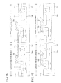
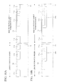
- Figs. 9A to 9I are cross sectional views illustrating a method of manufacturing the semiconductor device of the first embodiment in the order of manufacturing processes. With reference to these drawings, the method of manufacturing the semiconductor device of the first embodiment will be described.
- the p-type silicon semiconductor substrate 10 is prepared as illustrated in Fig. 9A .
- the element isolation film 11a defining the LDMOS transistor formation region and the ESD protection element formation region is formed in the semiconductor substrate 10 by use of a known shallow trench isolation (STI) method.
- the element isolation film 11b is formed in the LDMOS transistor formation region and the element isolation films 11c, 11d are formed in the ESD protection element formation region.
- trenches with a depth of 350 nm are formed in a predetermined pattern in the semiconductor substrate 10 by using a photolithography method and etching method. Then, an insulating substance such as a silicon oxide or a silicon nitride is filled into the trenches to form the element isolation film 11a and the element isolation films 11b, 11c, 11d.
- an insulating substance such as a silicon oxide or a silicon nitride is filled into the trenches to form the element isolation film 11a and the element isolation films 11b, 11c, 11d.
- the distance between the element isolation film 11b and the element isolation film 11a on one side is 2.8 ⁇ m
- the distance between the element isolation film 11b and the element isolation film 11a on the other side is 1.62 ⁇ m
- the width of the element isolation film 11b is 1.5 ⁇ m.
- the distance between the element isolation film 11c and the element isolation film 11a on one side is 2.8 ⁇ m
- the distance between the element isolation film 11c and the element isolation film 11d is 1.62 ⁇ m
- the distance between the element isolation film 11d and the element isolation film 11a on the other side is 1.62 ⁇ m
- the width of the element isolation film 11c is 3 ⁇ m
- the width of the element isolation film 11d is 0.24 ⁇ m.
- the surface of the semiconductor substrate 10 is thermally oxidized to form an oxide film 13 with a thickness of, for example, 10 nm.
- a process performed to obtain a structure in Fig. 9B will be explained.
- a photoresist is applied onto the oxide film 13 to form a photoresist film (not illustrated).
- exposure and development processes are performed on the photoresist film to provide the photoresist film with opening portions at lcoations corresponding to the LDMOS transistor formation region and the ESD protection element formation region.
- n-type impurity ions are implanted into the semiconductor substrate 10 through the opening portions.
- first ion implantation conditions are an implantation energy of 2.0 MeV and a dose of 2.5 ⁇ 10 12 cm -2
- second ion implantation conditions are an implantation energy of 500 keV and a dose of 1.5 ⁇ 10 12 cm -2 .
- the ion implantation into the semiconductor substrate 10 may be completed by performing two or more times of ion implantations as described above, or one time of ion implantation.
- the n-type drift region 14a is formed in the LDMOS transistor formation region, and the n-type drift region 14b is formed in the ESD protection element formation region. Then, the photoresist film is removed.
- a process performed to obtain a structure in Fig. 9C will be described.
- a photoresist is applied onto the oxide film 13 to form a photoresist film 15.
- the photoresist film 15 is processed by the exposure and development processes and thus is provided with opening portions at predetermined regions.
- p-type impurity ions are implanted into the semiconductor substrate 10 (drift regions 14a, 14b) through the opening portions.
- the p-type body region 16a is formed in the LDMOS transistor formation region and the p-type body region 16b is formed in the ESD protection element formation region.
- first ion implantation conditions are an implantation energy of 420 keV and a dose of 1 ⁇ 10 13 cm -2
- second ion implantation conditions are an implantation energy of 150 keV and a dose of 5 ⁇ 10 12 cm -2
- third ion implantation conditions are an implantation energy of 15 keV and a dose of 1 ⁇ 10 13 cm -2 .
- the dose into each of the body regions 16a, 16b has an influence on a threshold voltage of the transistor.
- the ion implantation to form the body regions 16a, 16b may be completed by performing two or more times of ion implantations as described above, or one time of ion implantation.
- the body region 16a in the LDMOS transistor formation region is in contact with the element isolation film 11a, but is away from the element isolation film 11b.
- the body region 16b in the ESD protection element formation region is also in contact with the element isolation film 11a, but is away from the element isolation film 11c.
- the photoresist film 15 used to form the body regions 16a, 16b is removed.
- a heat treatment at a temperature of 1000°C, for example, is performed to activate the impurities.
- the insulating film 13 damaged by the ion implantations and the like is removed.
- the surface of the semiconductor substrate 10 is again thermally oxidized to form the gate insulating film 17.
- the gate insulating film 17 has a thickness of 16 nm.
- a polysilicon film with a thickness of, for example, 180 nm is formed on the gate insulating film 17. Then, the polysilicon film is patterned by use of the photolithography method and etching method, and thereby the gate electrode 18a is formed in the LDMOS transistor formation region, and the gate electrode 18b is formed in the ESD protection element formation region.
- the gate electrode 18a is formed such that one end portion thereof in the width direction overlaps the body region 16a and the other end portion thereof overlaps the element isolation film 11b when the gate electrode 18a is viewed from above.
- the gate electrode 18b is formed such that one end portion thereof overlaps the body region 16b and the other end portion thereof overlaps the element isolation film 11c when the gate electrode 18b is viewed from above.
- the overlap length of the gate electrode 18b and the element isolation film 11c is set equal to the overlap length of the gate electrode 18a and the element isolation film 11b.
- the overlap length of the gate electrode 18b and the element isolation film 11c may be set slightly shorter than the overlap length of the gate electrode 18a and the element isolation film 11b.
- a process performed to obtain a structure in Fig. 9E will be explained.
- a photoresist film (not illustrated) provided with opening portions in a predetermined pattern is formed on top of the semiconductor substrate 10.
- n-type impurity ions are implanted into the semiconductor substrate 10 through the opening portions of the photoresist film to form the source regions 19a, 19b and the drain regions 20a, 20b.
- the ion implantation is performed by using P (phosphorus) as the n-type impurity under conditions of, for example, an implantation energy of 35 keV and a dose of 3.7 ⁇ 10 13 cm -2 .
- the source region 19a is formed in the upper portion of the body region 16a at a position adjacent to the gate electrode 18a and away from the element isolation film 11a when viewed from above.
- the source region 19b is formed in the upper portion of the body region 16b at a position adjacent to the gate electrode 18b and away from the element isolation film 11a when viewed from above.
- drain region 20a is formed between the element isolation film 11b and the element isolation film 11a and the drain region 20b is formed between the element isolation film 11d and the element isolation film 11a.
- an insulating film with a thickness of 100 nm made of a silicon oxide, a silicon nitride or the like is formed on the entire upper side of the semiconductor substrate 10 by use of the CVD method, for example. Thereafter, the insulating film is processed by anisotropic etching and thereby is left as the side walls 21 on both sides of each of the gate electrodes 18a, 18b. After that, a portion of the gate insulating film 17 not covered with the gate electrodes 18a, 18b and the side walls 21 is removed by etching.
- a process performed to obtain a structure in Fig. 9G will be explained.
- a photoresist film (not illustrated) provided with opening portions in a predetermined pattern is formed on top of the semiconductor substrate 10.
- p-type impurities are implanted into the semiconductor substrate 10 through the opening portions of the photoresist film to form the p-type high concentration impurity regions 22a, 22b and the anode region 22c.
- the ion implantation here is performed by using B (boron) as the p-type impurity under conditions of an implantation energy of 5 keV and a dose of 2 ⁇ 10 15 cm -2 .
- the p-type high concentration impurity region 22a is formed in a surface portion of the body region 16a between the source region 19a and the element isolation film 11a in the LDMOS transistor formation region.
- the p-type high concentration impurity region 22b is formed in a surface portion of the body region 16b between the source region 19b and the element isolation film 11a in the ESD protection element formation region, and the anode region 22c is formed between the element isolation film 11c and the element isolation film 11d.
- n-type impurities are implanted into the surface of the semiconductor substrate 10 through the opening portions to form the n-type high concentration impurity regions 23a, 23b, 23c, 23d.
- the ion implantation herein is performed by using P (phosphorus) as the n-type impurities under conditions of an implantation energy of 15 keV and a dose of 2 ⁇ 10 15 cm -2 .
- the n-type high concentration impurity region 23a is formed in a surface portion of the source region 19a between the p-type high concentration impurity region 22a and one of the side walls 21, and the n-type high concentration impurity region 23b is formed in a surface portion of the drain region 20a.
- the n-type high concentration impurity region 23c is formed in a surface portion of the source region 19b between the p-type high concentration impurity region 22b and one of the side walls 21, and the n-type high concentration impurity region 23d is formed in a surface portion of the drain region 20b.
- a process performed to obtain a structure in Fig. 9I will be explained.
- the photoresist film used to form the n-type high concentration impurity regions 23a, 23b, 23c, 23d is removed.
- a heat treatment at a temperature of 1000°C, for example, is performed to activate the impurities.
- a metal film made of Co (cobalt) or the like is formed on the entire upper side of the semiconductor substrate 10 and is processed by a heat treatment. With this heat treatment, the silicon in the surface of the semiconductor substrate 10 and the surface of the gate electrodes 18a, 18b react with metal elements in the metal film to form a siliside. Then, the metal film left unreacted is removed.
- Co cobalt
- the silicide film 25a is formed on the surfaces of the p-type high concentration impurity region 22a and the n-type high concentration impurity region 23a and the silicide film 25b is formed on the upper surface of the gate electrode 18a. Moreover, the silicide film 25c is formed on the surface of the n-type high concentration impurity region 23b.
- the silicide film 25d is formed on the surfaces of the p-type high concentration impurity region 22b and the n-type high concentration impurity region 23c, and the silicide film 25e is formed on the upper surface of the gate electrode 18b.
- the silicide film 25f is formed on the surface of the anode region 22c and the silicide film 25g is formed on the surface of the n-type high concentration impurity region 23d.
- an insulating substance such for example as a silicon oxide or a silicon nitride is deposited on the entire upper side of the semiconductor substrate 10 by using the CVD method or the like, and thereby the interlayer insulating film 27 is formed.
- the interlayer insulating film 27 may be formed of a single insulating film or a stack of two or more insulating films. Thereafter, the surface of the interlayer insulating film 27 is polished and flattened by the CMP method.
- contact halls are formed to extend from the surface of the interlayer insulating film 27 down to the silicide films 25a, 25b, 25c, 25d, 25e, 25f, 25g, respectively.
- a conductive material such as W (tungsten) is filled into these contact halls to form conductive plugs 26a, 26b, 26c, 26d, 26e, 26f, 26g.
- a conductive film is formed of aluminum or the like on the entire upper side of the semiconductor substrate 10, and thereafter the conductive film is patterned by use of the photolithography method and the etching method. In this way, the first layer of the interconnection 28 is formed in a predetermined pattern.
- the interlayer insulating film formation process, the conductive plug formation process, and the interconnection layer formation process are repeatedly performed to form a multi-layer interconnection structure.
- a protection film is formed on the multi-layer interconnection structure.
- the protection film on a lead electrode is etched by use of the photolithography method and the etching method. In this way, the semiconductor device including the LDMOS transistor and the ESD protection element according to the present embodiment is completed.
- the present embodiment involves a small number of manufacturing processes because the LDMOS transistor and the ESD protection element are formed at the same time. Thus, the present embodiment produces an effect of reduction in product costs.
- Figs. 10A to 10D are cross sectional views illustrating a method of manufacturing the semiconductor device of a second embodiment in the order of manufacturing processes.
- Fig. 11 is a top view of a semiconductor device according to the second embodiment.
- a p-type silicon semiconductor substrate 10 is prepared as illustrated in Fig. 10A .
- an element isolation film 11a is formed in the semiconductor substrate 10 to define an LDMOS transistor formation region and an ESD protection element formation region in the same method as in the first embodiment.
- an element isolation film 11b is formed in the LDMOS transistor formation region and element isolation films 11c, 11d are formed in the ESD protection element formation region.
- the surface of the semiconductor substrate 10 is thermally oxidized to form an oxide film 13.
- a process performed to obtain a structure in Fig. 10B will be explained.
- a photoresist film (not illustrated) is formed on the oxide film 13.
- the photoresist film is processed by exposure and development processes, and thereby is provided with opening portions at predetermined regions. Thereafter, n-type impurity ions are implanted into the semiconductor substrate 10 through the opening portions.
- the ion implantation herein is performed by using P (phosphorus) as the n-type impurities under conditions of an implantation energy of 300 keV to 2.0 MeV, and a dose of 10 12 cm -2 to 3 ⁇ 10 13 cm -2 .
- This ion implantation may be completed by performing one time of ion implantation or two or more times of ion implantations.
- drift region 34a is formed in the LDMOS transistor formation region and a drift region 34b is formed in the ESD protection element formation region.
- the drift region 34a in the LDMOS transistor formation region surrounds the element isolation film 11b, and is away from the element isolation film 11a on one side (the left side in Fig. 10B ) but is in contact with the element isolation film 11a on the other side (the right side in Fig. 10B ).
- the drift region 34b in the ESD protection element formation region surrounds the element isolation films 11c, 11d, and is away from the element isolation film 11a on one side (the left side in Fig. 10B ) but is in contact with the element isolation film 11a on the other side (the right side in Fig. 10B ).
- a process performed to obtain a structure in Fig. 10C will be explained.
- a photoresist film (not illustrated) is formed on the oxide film 13 and the photoresist film is processed by exposure and development processes, and thereby is provided with opening portions at predetermined regions.
- p-type impurity ions are implanted into the semiconductor substrate 10 through the opening portions.
- a p-type body region 16a is formed in the LDMOS transistor formation region
- a p-type body region 16b is formed in the ESD protection element formation region.
- the ions are implanted into the semiconductor substrate 10 under conditions of an implantation energy of 150 keV to 500 keV and a dose of 10 12 cm -2 to 3 ⁇ 10 13 cm -2 .
- This ion implantation may be completed by performing one time of ion implantation or two or more times of ion implantations.
- the body region 16a is formed between the drift region 34a and the element isolation film 11a on one side (the left side in Fig. 10C ) in the LDMOS transistor formation region.
- the body region 16b is formed between the drift region 34b and the element isolation film 11a on one side (the left side in Fig. 10C ) in the ESD protection element formation region.
- a process performed to obtain a structure in Fig. 10D will be explained.
- the photoresist film used to form the body regions 16a, 16b is removed.
- a heat treatment at a temperature of 1000°C, for example, is performed to activate the impurities.
- the heat treatment is performed again to thermally oxidize the surface of the substrate 10 to form a gate insulating film 17.
- gate electrodes 18a, 18b made of a polysilicon, for example, are formed on the gate insulating film 17.
- the gate electrode 18a is formed such that one end portion thereof in the width direction overlaps the body region 16a and the other end portion thereof overlaps the element isolation film 11b when the gate electrode 18a is viewed from above.
- the gate electrode 18b is formed such that one end portion thereof in the width direction overlaps the body region 16b and the other end portion thereof overlaps the element isolation film 11c when the gate electrode 18b is viewed from above.
- the distance (B2 in Fig. 11 ) between the edge portion of the gate electrode 18b and the edge portion of the element isolation film 11c on the other side is larger than the distance (B1 in Fig. 11 ) between the edge portion of the gate electrode 18a and the edge portion of the element isolation film 11b on the other side (B1 ⁇ B2).
- a photoresist film is formed on top of the semiconductor substrate 10, and is processed by exposure and development processes thereby to be provided with opening portions at predetermined regions. Thereafter, n-type impurity ions are implanted into the semiconductor substrate 10 through the opening portions to form source regions 19a, 19b and drain regions 20a, 20b.
- the source region 19a is formed in an upper portion of the body region 16a at a position adjacent to the gate electrode 18a and away from the element isolation film 11a when viewed from above.
- the source region 19b is formed in an upper portion of the body region 16b at a position adjacent to the gate electrode 18b and away from the element isolation film 11a when viewed from above.
- drain region 20a is formed between the element isolation film 11b and the element isolation film 11a
- drain region 20b is formed between the element isolation film 11d and the element isolation film 11a.
- an insulating film is formed on the enter upper side of the semiconductor substrate 10.
- the insulating film is processed by anisotropic etching to form side walls 21 on both sides of each of the gate electrodes 18a, 18b. Thereafter, a portion of the gate insulating film 17 not covered with the gate electrodes 18a, 18b and the side walls 21 is removed by etching.
- a photoresist film is formed on top of the semiconductor substrate 10 and is processed by exposure and development processes to be provided with opening portions at predetermined regions. After that, p-type impurities are implanted into the semiconductor substrate 10 through the opening portions to form p-type high concentration impurity regions 22a, 22b and an anode region 22c.
- the p-type high concentration impurity region 22a is formed in a surface portion of the body region 16a between the source region 19a and the element isolation film 11a in the LDMOS transistor formation region.
- the p-type high concentration impurity region 22b is formed in a surface portion of the body region 16b between the source region 19b and the element isolation film 11a in the ESD protection element formation region.
- the anode region 22c is formed between the element isolation film 11c and the element isolation film 11d.
- the photoresist film used to form the p-type high concentration impurity regions 22a, 22b and the anode region 22c is removed.
- a photoresist film is formed on top of the semiconductor substrate 10, and is processed by exposure and development processes to be provided with opening portions at predetermined regions. Thereafter, n-type impurities are implanted into the semiconductor substrate 10 through the opening portions to form n-type high concentration impurity regions 23a, 23b, 23c, 23d.
- the n-type high concentration impurity region 23a is formed in a surface portion of the source region 19a between the p-type high concentration impurity region 22a and one of the side walls 21, and the n-type high concentration impurity region 23b is formed in a surface portion of the drain region 20a.
- the n-type high concentration impurity region 23c is formed in a surface portion of the source region 19b between the p-type high concentration impurity region 22b and one of the side walls 21.
- the n-type high concentration impurity region 23d is formed in a surface portion of the drain region 20b.
- the photoresist film used to form the n-type high concentration impurity regions 23a, 23b, 23c, 23d is removed and then a heat treatment at a temperature of 1000°C, for example, is performed to activate the impurities.
- a heat treatment at a temperature of 1000°C, for example is performed to activate the impurities.
- the distance B2 between the edge portion of the gate electrode 18b and the anode region 22c in the ESD protection element is set larger than the distance B1 between the edge portion of the gate electrode 18a and the drain region 20a in the LDMOS transistor (B1 ⁇ B2).
- these settings may enable the ESD protection element to prevent the internal circuit from being broken down due to static electricity or the like, and also allow the semiconductor device to achieve a higher integration.
- the LDMOS transistor and the ESD protection element are formed at the same time, which produces effects of avoiding an increase in the number of manufacturing processes and thereby reducing the manufacturing costs.
- Figs. 12A to 12D are cross sectional views illustrating a method of manufacturing a semiconductor device of a third embodiment in the order of manufacturing processes.
- Fig. 13 is a top view of the semiconductor device of the third embodiment.
- a p-type silicon semiconductor substrate 10 is prepared as illustrated in Fig. 12A .
- an element isolation film 11a is formed in the semiconductor substrate 10 to define an LDMOS transistor formation region and an ESD protection element formation region.
- an element isolation film 11b is formed in the LDMOS transistor formation region and element isolation films 11c, 11d are formed in the ESD protection element formation region.
- the surface of the semiconductor substrate 10 is thermally oxidized to form an oxide film 13.
- a process performed to obtain a structure in Fig. 12B will be explained.
- a photoresist film (not illustrated) is formed on the oxide film 13.
- the photoresist film is processed by exposure and development processes to be provided with opening portions at predetermined regions.
- p-type impurity ions are implanted into the semiconductor substrate 10 through the opening portions.
- the ion implantation is performed by using B (boron) as the p-type impurity under conditions of an implantation energy of 150 keV to 1.0 MeV and a dose of 10 12 cm -2 to 3 ⁇ 10 13 cm -2 .
- This ion implantation may be completed by performing one time of ion implantation or two or more times of ion implantations.
- a p-type body region 46a is formed in the LDMOS transistor formation region and a p-type body region 46b is formed in the ESD protection element formation region.
- a process performed to obtain a structure in Fig. 12C will be explained.
- a photoresist film is formed on the oxide film 13, and then is processed by exposure and development processes to be provided with opening portions at predetermined regions.
- n-type impurity ions are implanted into the body regions 46a, 46b through the opening portions to form an n-type drift region 44a in the LDMOS transistor formation region and an n-type drift region 44b in the ESD protection element formation region.
- the drift region 44a in the LDMOS transistor formation region surrounds the element isolation film 11b, and is away from the element isolation film 11a on one side (the left side in Fig. 12C ) but is in contact with the element isolation film 11a on the other side (the right side in Fig. 12C ).
- the drift region 44b in the ESD protection element formation region surrounds the element isolation films 11c, 11d, and is away from the element isolation film 11a on one side (the left side in Fig. 12C ) but is in contact with the element isolation film 11a on the other side (the right side in Fig. 12C ).
- the photoresist film used to form the drift regions 44a, 44b is removed. Then, as is the case with the first embodiment, a heat treatment at a temperature of 1000°C, for example, is performed to activate the impurities. Then, the insulating film 13 is removed, and the heat treatment is performed again to thermally oxidize the surface of the substrate 10, and thereby to form a gate insulating film 17.
- gate electrodes 18a, 18b made of a polysilicon, for example, are formed on the gate insulating film 17.
- the gate electrode 18a is formed such that one end portion thereof in the width direction overlaps the body region 46a and the other end portion thereof overlaps the element isolation film 11b when the gate electrode 18a is viewed from above.
- the gate electrode 18b is formed such that one end portion thereof in the width direction overlaps the body region 46b and the other end portion thereof overlaps the element isolation film 11c when the gate electrode 18b is viewed from above.
- the distance (B2 in Fig. 13 ) between the edge portion of the gate electrode 18b and the edge portion of the element isolation film 11c on the other side is larger than the distance (B1 in Fig. 13 ) between the edge portion of the gate electrode 18a and the edge portion of the element isolation film 11b on the other side (B1 ⁇ B2).
- a photoresist film is formed on top of the semiconductor substrate 10 and is processed by exposure and development processes to be provided with opening portions at predetermined regions. Thereafter, n-type impurity ions are implanted into the semiconductor substrate 10 through the opening portions to form source regions 19a, 19b and drain regions 20a, 20b.
- the source region 19a is formed in an upper portion of the body region 46a at a position adjacent to the gate electrode 18a and away from the element isolation film 11a when viewed from above.
- the source region 19b is formed in an upper portion of the body region 46b at a position adjacent to the gate electrode 18b and away from the element isolation film 11a when viewed from above.
- drain region 20a is formed between the element isolation film 11b and the element isolation film 11a
- drain region 20b is formed between the element isolation film 11d and the element isolation film 11a.
- an insulating film is formed on the enter upper side of the semiconductor substrate 10.
- the insulating film is processed by anisotropic etching to form side walls 21 on both sides of each of the gate electrodes 18a, 18b. Thereafter, a portion of the gate insulating film 17 not covered with the gate electrodes 18a, 18b and the side walls 21 is removed by etching.
- a photoresist film is formed on top of the semiconductor substrate 10 and is processed by exposure and development processes to be provided with opening portions at predetermined regions. After that, p-type impurities are implanted into the semiconductor substrate 10 through the opening portions to form p-type high concentration impurity regions 22a, 22b and an anode region 22c.
- the p-type high concentration impurity region 22a is formed in a surface portion of the body region 46a between the source region 19a and the element isolation film 11a in the LDMOS transistor formation region.
- the p-type high concentration impurity region 22b is formed in a surface portion of the body region 46b between the source region 19b and the element isolation film 11a in the ESD protection element formation region.
- the anode region 22c is formed between the element isolation film 11c and the element isolation film 11d.
- a photoresist film is formed on top of the semiconductor substrate 10 and is processed by exposure and development processes to be provided with opening portions at predetermined regions. Then, n-type impurities are implanted into the semiconductor substrate 10 through the opening portions to form n-type high concentration impurity regions 23a, 23b, 23c, 23d.
- the n-type high concentration impurity region 23a is formed in a surface portion of the source region 19a between the p-type high concentration impurity region 22a and one of the side walls 21, and the n-type high concentration impurity region 23b is formed in a surface portion of the drain region 20a.
- the n-type high concentration impurity region 23c is formed in a surface portion of the source region 19b between the p-type high concentration impurity region 22b and one of the side walls 21.
- the n-type high concentration impurity region 23d is formed in a surface portion of the drain region 20b.
- the photoresist film used to form the n-type high concentration impurity regions 23a, 23b, 23c, 23d is removed and then a heat treatment at a temperature of 1000°C, for example, is performed to activate the impurities.
- a heat treatment at a temperature of 1000°C, for example is performed to activate the impurities.
- the distance B2 between the edge portion of the gate electrode 18b and the anode region 22c in the ESD protection element is set larger than the distance B1 between the edge portion of the gate electrode 18a and the drain region 20a in the LDMOS transistor (B1 ⁇ B2).
- these settings may enable the ESD protection element to prevent the internal circuit from being broken down due to static electricity or the like, and also allow the semiconductor device to achieve a higher integration.
- the LDMOS transistor and the ESD protection element are formed at the same time, which produces effects of avoiding an increase in the number of manufacturing processes and thereby reducing the manufacturing costs.
- Fig. 14 is a cross sectional view illustrating a semiconductor device according to a fourth embodiment.
- Fig. 15 is a top view of the semiconductor device of the fourth embodiment.
- the same reference numerals are attached to the same portions as those in Figs. 1 and 2 , and the detailed description thereof is omitted.
- the illustrations of the silicide film, the interlayer insulating film and the like are omitted in Figs. 14 and 15 .
- an element isolation film 11a is formed as in the case of the first embodiment, and thereby an LDMOS transistor formation region and an ESD protection element formation region are defined by the element isolation film 11a.
- an element isolation film 11b is formed in the LDMOS transistor formation region and element isolation films 11c, 11d are formed in the ESD protection element formation region.
- an n-type drift region 14a, a p-type body region 16a, an n-type source region 19a, an n-type drain region 20a, a p-type high concentration impurity region 22a, and n-type high concentration impurity regions 23a, 23b are formed in the LDMOS transistor formation region.
- an n-type drift region 14b, a p-type body region 16b, an n-type source region 19b, a p-type anode region 22c, an n-type drain region 20b, a p-type high concentration impurity region 22b, and n-type high concentration impurity regions 23c, 23d are formed in the ESD protection element formation region.
- a gate electrode 58a in a rectangular ring shape is formed on the semiconductor substrate 10 with the gate insulating film 17 interposed in between.
- the p-type high concentration impurity region 22a and the n-type high concentration impurity region 23a are disposed inside the gate electrode 58a in the ring shape.
- a gate electrode 58b in a rectangular ring shape is formed on the semiconductor substrate 10 with the gate insulating film 17 interposed in between.
- the p-type high concentration impurity region 22b and the n-type high concentration impurity region 23c are disposed inside the gate electrode 58b in the ring shape.
- the distance (B2 in Fig. 15 ) between the edge portion of the gate electrode 58b and the edge portion of the element isolation film 11c on the other side is set larger than the distance (B1 in Fig. 15 ) between the edge portion of the gate electrode 18a and the edge portion of the element isolation film 11b on the other side (B1 ⁇ B2).
- these settings may enable the ESD protection element to prevent the internal circuit from being broken down due to static electricity or the like, and also allow the semiconductor device to achieve a higher integration.
- the LDMOS transistor and the ESD protection element are formed at the same time, which produces effects of avoiding an increase in the number of manufacturing processes and thereby reducing the manufacturing costs.
- the gate electrodes 58a, 58b are formed in the ring shapes. Due to the bias of the gate electrodes 58a, 58b, the depletion layers expand in the drift regions 14a, 14b with relatively higher concentration. This produces an advantageous effect of obtaining the desired characteristic (junction breakdown voltage) of the semiconductor device.
Landscapes
- Semiconductor Integrated Circuits (AREA)
- Insulated Gate Type Field-Effect Transistor (AREA)
- Metal-Oxide And Bipolar Metal-Oxide Semiconductor Integrated Circuits (AREA)
Abstract
A gate electrode, an element isolation film and a drain region in an LDMOS transistor formation region and a gate electrode, an element isolation film and an anode region in an ESD protection element formation region are formed to satisfy relationships of A1 = A2 and B1 < B2 where the LDMOS transistor formation region has an overlap length A1 of the gate electrode and the element isolation film and a distance B1 between the gate electrode and the drain region, and the ESD protection element formation region has an overlap length A2 of the gate electrode and the element isolation film and a distance B2 between the gate electrode and the anode region.
Description
- The embodiments discussed herein relate to a semiconductor device including a laterally diffused metal oxide semiconductor (LDMOS) transistor and an electrostatic discharge (ESD) protection element, and a method of manufacturing the semiconductor device.
- Heretofore, compound semiconductor elements have been mainly used to process signals at high frequency band (microwave band). In recent years, however, laterally diffused metal oxide semiconductor (LDMOS) transistors formed in semiconductor substrates have been used instead of these compound semiconductor elements. The LDMOS transistors are advantageous in that the LDMOS transistors can be fabricated at lower costs than the compound semiconductor elements. In addition, the LDMOS transistors are also advantageous in that the breakdown voltage thereof can be enhanced relatively easily. Semiconductor devices (integrated circuits) each internally including an LDMOS transistor are widely used in mobile phones, wireless LAN equipment, in-vehicle electronic devices, and the like.
- In addition, there are many semiconductor devices each including an electrostatic discharge (ESD) protection element in a chip to prevent an electrostatic breakdown of the device. There are also developed thyristor-type ESD protection elements achieving high discharge performance with almost the same structure as LDMOS transistors.
- Patent Document 1:
US patent No. 5903032 - Patent Document 2:
US patent No.6144070 - Patent Document 3: Japanese Laid-open Patent Application Publication No.
2001-320047 - Patent Document 4: Japanese Laid-open Patent Application Publication No.
2002-94063 - Embodiments of the present invention provide a semiconductor device, and a method of manufacturing the same, the semiconductor device including an LDMOS transistor and an ESD protection element, being producible in simple manufacturing processes and enabling higher integration while ensuring a desired characteristic.
- According to an aspect of an embodiment of the present invention, there is provided a semiconductor device including a LDMOS (Laterally Diffused MOS) transistor and an ESD (Electrostatic Discharge) protection element. The LDMOS transistor includes: a first gate electrode formed on the semiconductor substrate with an insulating film interposed therebetween; a first body region formed by implanting impurities of a first conductivity type into the semiconductor substrate and disposed at one edge side of the first gate electrode; a first source region of a second conductivity type disposed in an upper portion of the first body region; a first element isolation film formed in an upper portion of the semiconductor substrate and disposed to overlap the first gate electrode; a first drain region formed inside the semiconductor substrate, including impurities of the second conductivity type, and disposed at a position in contact with an edge portion of the first element isolation film and away from the first gate electrode; and a first drift region formed inside the semiconductor substrate, including impurities of the second conductivity type, and being in contact with the first body region and the first drain region. Meanwhile, the ESD protection element includes: a second gate electrode formed on the semiconductor substrate with an insulating film interposed therebetween; a second body region formed inside the semiconductor substrate, including impurities of the first conductivity type, and disposed at one edge side of the second gate electrode; a second source region of the second conductivity type disposed in an upper portion of the second body region; a second element isolation film formed in an upper portion of the semiconductor substrate and disposed to overlap the second gate electrode; an anode region formed inside the semiconductor substrate, including impurities of the first conductivity type, and disposed at a position in contact with an edge portion of the second element isolation film and away from the second gate electrode; a third element isolation film formed in an upper portion of the semiconductor substrate and disposed adjacent to the anode region; a second drain region formed inside the semiconductor substrate, including impurities of the second conductivity type, and being in contact with the third element isolation film; and a second drift region formed inside the semiconductor substrate, including impurities of the second conductivity type, and being in contact with the second body region, the anode region and the second drain region. The semiconductor device has relationships of A1 = A2 and B1 < B2 where A1 denotes an overlap length of the first gate electrode and the first element isolation film; A2 denotes an overlap length of the second gate electrode and the second element isolation film; B1 denotes a distance between the first gate electrode and the first drain region; and B2 denotes a distance between the second gate electrode and the anode region.
- According to the semiconductor device of the above aspect, the LDMOS transistor and the ESD protection element may be formed simultaneously, which avoid an increase in the number of manufacturing processes. In addition, the semiconductor device obtains a desirable characteristic while suppressing an enlargement of an element region. Thus, higher integration of semiconductor devices may be achieved.
- The invention will now be described, by way of examples only, with reference to the following drawings in which:
-
Fig. 1 is a cross sectional view of a semiconductor device of a first embodiment; -
Fig. 2 is a layout of the semiconductor device of the first embodiment; -
Fig. 3 is a view explaining relationships between an overlap length A1 of an element isolation film and a gate electrode above the element isolation film and a distance B1 between an edge portion of the gate electrode and a drain region in an LDMOS transistor formation region; and an overlap length A2 of an element isolation film and a gate electrode above the element isolation film and a distance B2 between an edge portion of the gate electrode and an anode region in an ESD protection element formation region; -
Fig. 4 is a diagram explaining an operation of an ESD protection element; -
Fig. 5 is a diagram exemplifying a relationship between a breakdown voltage and the overlap length of the gate electrode and the element isolation film; -
Fig. 6A is a cross sectional view of a semiconductor device according to the embodiment and a comparative example,Fig. 6B is a cross sectional view of the ESD protection element in the semiconductor device of the embodiment, andFig. 6C is a cross sectional view of an ESD protection element in the semiconductor device of the comparative example; -
Fig. 7 is a diagram illustrating simulation results of breakdown voltage characteristics of the ESD protection element in the embodiment and of the ESD protection element in the comparative example; -
Fig. 8 is a circuit diagram illustrating an example of an electronic circuit including the semiconductor device in the embodiment; -
Figs. 9A to 9I are cross sectional views illustrating a method of manufacturing the semiconductor device of the first embodiment; -
Figs. 10A to 10D are cross sectional views illustrating a method of manufacturing a semiconductor device of a second embodiment; -
Fig. 11 is a top view of the semiconductor device of the second embodiment; -
Figs. 12A to 12D are cross sectional views illustrating a method of manufacturing a semiconductor device of a third embodiment; -
Fig. 13 is a top view of the semiconductor device of the third embodiment; -
Fig. 14 is a cross sectional view of a semiconductor device according to a fourth embodiment; and -
Fig. 15 is a top view of the semiconductor device of the fourth embodiment. - Hereinafter, embodiments will be described by referring to the accompanying drawings.
-
Fig. 1 is a cross sectional view of a semiconductor device of a first embodiment, andFig. 2 is a layout of the semiconductor device. In the following description, a first conductivity type is p-type and a second conductivity type is n-type. However, the first conductivity type may be n-type and the second conductivity type may be p-type. - As illustrated in
Figs. 1 and2 , anelement isolation film 11a is formed in a predetermined region of a p-type (first conductivity type)silicon semiconductor substrate 10 and defines an LDMOS transistor formation region (referred to as an LDMOS formation region in the drawings: the same shall apply below) and an ESD protection element formation region. An LDMOS transistor is formed in the LDMOS transistor formation region and a thyristor-type ESD protection element is formed in the ESD protection element formation region. - To begin with, a structure of the LDMOS transistor is described. The LDMOS transistor formation region is surrounded by the
element isolation film 11a. This LDMOS transistor formation region is provided with adrift region 14a formed by introducing n-type (second conductivity type) impurities into thesemiconductor substrate 10. In addition, anelement isolation film 11b traversing the LDMOS transistor formation region is formed in a predetermined region in an upper portion of thesemiconductor substrate 10. - A
gate insulating film 17 is formed on thesemiconductor substrate 10 to run along almost the center of the LDMOS transistor formation region. A portion (a right side portion inFig. 1 ) of thegate insulating film 17 is arranged on theelement isolation film 11b. Agate electrode 18a traversing the LDMOS transistor formation region andside walls 21 arranged at both sides of thegate electrode 18a in a width direction are formed on thegate insulating film 17. In addition, asilicide film 25b is formed on an upper surface of thegate electrode 18a. - A
body region 16a formed by introducing p-type impurities is arranged at one side of thegate electrode 18a in the width direction (the left side inFigs. 1 and2 ). Asource region 19a formed by introducing n-type impurities is arranged in an upper portion of thebody region 16a. - An n-type high
concentration impurity region 23a into which n-type impurities are introduced at a higher concentration than in thesource region 19a is provide in an upper portion of thesource region 19a. A p-type highconcentration impurity region 22a into which p-type impurities are introduced at a higher concentration than in thebody region 16a is provided in an upper portion of thebody region 16a between the n-type highconcentration impurity region 23a and theelement isolation film 11a. - A
silicide film 25a is formed on surfaces of the n-type highconcentration impurity region 23a and the p-type highconcentration impurity region 22a. The n-type highconcentration impurity region 23a and the p-type highconcentration impurity region 22a are electrically connected to each other through thesilicide film 25a. - In this embodiment, the n-type high
concentration impurity region 23a and the p-type highconcentration impurity region 22a are in contact with each other, but an element isolation film may be formed between theseimpurity regions - In the LDMOS transistor formation region, a
drain region 20a formed by introducing n-type impurities is arranged between theelement isolation film 11b and theelement isolation film 11a on the opposite side in the width direction (the right side inFig. 1 ). An n-type highconcentration impurity region 23b into which n-type impurities are introduced at a higher concentration than in thedrain region 20a is provided in an upper portion of thedrain region 20a and asilicide film 25c is formed on a surface of the n-type highconcentration impurity region 23b. - An interlayer insulating
film 27 is formed on top of thesemiconductor substrate 10 in the LDMOS transistor formation region, and thegate electrode 18a is covered with theinterlayer insulating film 27. Thesilicide films interlayer insulating film 27 throughconductive plugs - Next, a structure of the ESD protection element is described. The ESD protection element formation region is also surrounded by the
element isolation film 11a. The ESD protection element formation region is also provided with adrift region 14b formed by introducing n-type impurities into thesemiconductor substrate 10. In addition,element isolation films semiconductor substrate 10. Theelement isolation films - A
gate insulating film 17 is formed on thesemiconductor substrate 10 to traverse the ESD protection element formation region. A portion (a right side portion inFig. 1 ) of thegate insulating film 17 is arranged on theelement isolation film 11c. Agate electrode 18b traversing the ESD protection element formation region andside walls 21 arranged at both sides of thegate electrode 18b in the width direction are formed on thegate insulating film 17. In addition, asilicide film 25e is formed on an upper surface of thegate electrode 18b. - A
body region 16b formed by introducing p-type impurities is arranged at one side of thegate electrode 18b in the width direction (the left side inFigs. 1 and2 ). Asource region 19b formed by introducing n-type impurities is arranged in an upper portion of thebody region 16b. - An n-type high
concentration impurity region 23c into which n-type impurities are introduced at a higher concentration than in thesource region 19b is provide in an upper portion of thesource region 19b. A p-type highconcentration impurity region 22b into which p-type impurities are introduced at a higher concentration than in thebody region 16b is provided in an upper portion of thebody region 16b between the n-type highconcentration impurity region 23c and theelement isolation film 11a. - A
silicide film 25d is formed on surfaces of the n-type highconcentration impurity region 23c and the p-type highconcentration impurity region 22b. The n-type highconcentration impurity region 23c and the p-type highconcentration impurity region 22b are electrically connected to each other through thesilicide film 25d. - In this embodiment, the n-type high
concentration impurity region 23c and the p-type highconcentration impurity region 22b are in contact with each other, but an element isolation film may be formed between theseimpurity regions - In the ESD protection element formation region, an
anode region 22c formed by introducing p-type impurities is formed between theelement isolation film 11c and theelement isolation film 11d. Asilicide film 25f is formed on a surface of theanode region 22c. - In the ESD protection element formation region, a
drain region 20b formed by introducing n-type impurities is arranged between theelement isolation film 11d and theelement isolation film 11a on the opposite side (the right side inFig. 1 ). An n-type highconcentration impurity region 23d into which n-type impurities are introduced at a higher concentration than in thedrain region 20b is provided in an upper portion of thedrain region 20b and asilicide film 25g is formed on a surface of the n-type highconcentration impurity region 23d. - The
interlayer insulating film 27 is also formed on top of thesemiconductor substrate 10 in the ESD protection element formation region, and thegate electrode 18b is covered with theinterlayer insulating film 27. Thesilicide films interlayer insulating film 27 throughconductive plugs - Here, as illustrated in
Figs. 2 and3 , in the LDMOS transistor formation region, A1 denotes the length of a portion where theelement isolation film 11b overlaps thegate electrode 18a above theelement isolation film 11b, and B1 denotes a distance between an edge portion of thegate electrode 18a and thedrain region 20a (that is, a distance in a direction parallel to the substrate surface). In addition, in the ESD protection element formation region, A2 denotes a length of a portion where theelement isolation film 11c overlaps thegate electrode 18b above theelement isolation film 11c, and B2 denotes a distance between an edge portion of thegate electrode 18b and theanode region 22c (that is, a distance in the direction parallel to the substrate surface). In this case, the semiconductor device of the present embodiment has relationships of A1 = A2 and B1 < B2. - Hereinafter, the ESD protection element with the foregoing structure will be described in more detail. For instance, as illustrated in
Fig. 3 , thesource region 19b, thebody region 16b and thegate electrode 18b in the ESD protection element are connected to a single terminal T1. In addition, theanode region 22c and thedrain region 20b are connected to a single terminal T2. The terminal T1 is connected to a low potential terminal of an internal circuit (the circuit including the LDMOS transistor), and the terminal T2 is connected to a high potential terminal of the internal circuit, for example. -
Fig. 4 is a diagram explaining an operation of the ESD protection element with a voltage on the horizontal axis and an electric current on the vertical axis. Here, an operation voltage in the internal circuit of the semiconductor device (a highest voltage applied between the terminals T1 and T2 in a normal operation) is denoted by VDD, an operation start voltage of the ESD protection element is denoted by Vt1, and a voltage to break down the internal circuit (hereinafter, referred to as a breakdown voltage) is denoted by VDDMAX. It is important that the operation start voltage Vt1 of the ESD protection element is higher than the operation voltage VDD of the internal circuit and is lower than the breakdown voltage VDDMAX. - The ESD protection element is in an off state when the voltage applied to the internal circuit is lower than the operation start voltage Vt1. When a higher voltage is applied between the terminals T1, T2 due to static electricity or the like, the ESD protection element is turned into an on state and an electric current flows into the ESD protection element. At this time, the electric current flowing through the ESD protection element causes a change in the voltage between the terminals T1, T2. Here, what is important is that even the peak voltage between the terminals T1, T2 does not exceed the breakdown voltage VDDMAX.
- When the voltage is applied between the terminals T1, T2, a depletion layer expands between the
body region 16b and thedrift region 14b and a depletion layer expands between thedrift region 14b and theanode region 22c. Consequently, a punch-through more likely occurs. The punch-through is a phenomenon in which the depletion layer between thebody region 16b and thedrift region 14b and the depletion layer between thedrift region 14b and theanode region 22c are connected to each other to cause a large electric current to flow. - One possible method to prevent a punch-through is to make the impurity concentration of the
drift region 14b in the ESD protection element formation region higher than the impurity concentration of thedrift region 14a in the LDMOS transistor formation region. In this case, however, since a junction breakdown voltage between thebody region 16b and thedrift region 14b is lowered, the operation start voltage Vt1 of the ESD protection element may become lower than the operation voltage VDD of the LDMOS transistor even though the punch-through is prevented. In addition, there also arises another problem of an increase in the number of manufacturing processes. - Another possible method to prevent a punch-through is to increase the distance between the
body region 16b and theanode region 22c. A simple increase in the distance between thebody region 16b and theanode region 22c, however, may raise the junction breakdown voltage between thebody region 16b and thedrift region 14b and thereby make the operation start voltage Vt1 of the ESD protection element higher than the breakdown voltage VDDMAX of the internal circuit. Moreover, this method impedes achievement of higher integration of the semiconductor device. - In the LDMOS transistor, the junction breakdown voltage between the body region and the drift region largely depends on the length (overlap length) of the portion where the element isolation film overlaps the gate electrode.
-
Fig. 5 is a diagram exemplifying a relationship between a breakdown voltage and the overlap length of the gate electrode and the element isolation film, with the breakdown voltage on the vertical axis and the overlap length on the horizontal axis. - As is apparent from
Fig. 5 , the junction breakdown voltage betweenbody region region gate electrode element isolation film gate electrode drift region - When the overlap length A2 is made longer than the overlap length A1 (A1<A2), the junction breakdown voltage between the
drift region 14b and thebody region 16b in the ESD protection element becomes higher than the junction breakdown voltage between thedrift region 14a and thebody region 16a in the LDMOS transistor. As a result, the operation start voltage Vt1 of the ESD protection element may become higher than the breakdown voltage VDDMAX of the internal circuit, in some cases. - To prevent this, in the present embodiment, the overlap length A2 of the
gate electrode 18b and theelement isolation film 11c in the ESD protection element is set equal to or slightly shorter than the overlap length A1 of thegate electrode 18a and theelement isolation film 11b in the LDMOS transistor (A1 = A2). With this setting, the junction breakdown voltage between thebody region 16b and thedrift region 14b in the ESD protection element is made equal to or slightly smaller than the junction breakdown voltage between thebody region 16a and thedrift region 14a in the LDMOS transistor. - In the present embodiment, the distance between the edge portion of the
gate electrode 18b and theanode region 22c is increased to prevent the occurrence of a punch-through. The increase in the distance between the edge portion of thegate electrode 18b and theanode region 22c may raise the junction breakdown voltage between thebody region 16b and thedrift region 14b in the ESD protection element in some cases depending on manufacturing conditions. This influence, however, is smaller than in the case where the overlap length of the gate electrode and the element isolation film is changed. - As described above, the distance between the edge portion of the
gate electrode 18b and theanode region 22c is increased. This increase more suppresses an enlargement of the ESD protection element formation region than in the case where the distance between the body region and the anode region is simply increased. In this way, the semiconductor device obtains a desirable characteristic while achieving higher integration. - Hereinafter, the characteristic of the ESD protection element of the semiconductor device according to the embodiment will be explained in comparison with a comparative example.
-
Fig. 6A is a cross sectional view of the LDMOS transistors of the semiconductor devices in the embodiment and the comparative example,Fig. 6B is a cross sectional view of the ESD protection element of the semiconductor device in the embodiment, andFig. 6C is a cross sectional view of the ESD protection element of the semiconductor device in the comparative example. InFigs 6A to 6C , the same portions as those inFig. 1 are indicated by the same reference numerals. In addition, inFigs 6A to 6C , illustrations of the silicide film, the interlayer insulating film and the like are omitted. Hereinafter, the ESD protection element of the semiconductor device in the embodiment is simply referred to as the ESD protection element in the embodiment, and the ESD protection element of the semiconductor device in the comparative example is simply referred to as the ESD protection element in the comparative example. - The ESD protection elements of the semiconductor devices in the embodiment and the comparative example are the same in shape and size. In the ESD protection element in the embodiment (see
Fig. 6B ), theanode region 22c is in contact with theelement isolation films Fig. 6C ), theanode region 22d is away from theelement isolation film 11c because theelement isolation film 11c has a smaller width. The ESD protection element in the embodiment and the ESD protection element in the comparative example are the same in the other portions. -
Fig. 7 is a diagram illustrating simulation results of breakdown voltage characteristics of the ESD protection element in the embodiment and the ESD protection element in the comparative example, with the distance between the gate electrode and the anode region on the horizontal axis and with the breakdown voltage on the vertical axis. Here, the overlap length of thegate electrode 18b and theelement isolation film 11c is 0.75 µm in both the ESD protection elements in the embodiment and the comparative example.Fig. 7 also illustrates the breakdown voltage characteristic of the LDMOS transistor. In the case of the LDMOS transistor, the horizontal axis indicates the distance between the gate electrode and the drain region. - As is apparent from
Fig. 7 , the ESD protection element in the embodiment is prevented from causing a punch-through if the distance between thegate electrode 18b and theanode region 22c is set to about 1.0 µm or longer. In contrast, the ESD protection element in the comparative example causes a punch-through when the distance between thegate electrode 18b and theanode region 22d is about 1.0 µm, and may need to be configured with the distance between thegate electrode 18b and theanode region 22d set to about 1.5 µm or longer to prevent a punch-through. - This is because, in the ESD protection element in the comparative example, the
anode region 22d is away from theelement isolation film 11c and therefore the depletion layer between thedrift region 14b and theanode region 22d is more likely to expand toward thebody region 16b than in the ESD protection element in the embodiment. - As is clear in
Fig. 7 , the ESD protection element in the embodiment has an almost constant operation start voltage Vt1 (=BVsd) even when the distance between thegate electrode 18b and theanode region 22c is changed. In other words, the operation start voltage Vt1 is determined by the overlap length of thegate electrode 18b and theelement isolation film 11c irrespective of the distance between thegate electrode 18b and theanode region 22c. -
Fig. 8 is a circuit diagram illustrating an example of an electronic circuit including the semiconductor device in the present embodiment. - An
output circuit 30 includes a p-type LDMOS transistor 31a and an n-type LDMOS transistor 31b. The source, gate and body of the p-type LDMOS transistor 31a are connected to a high potentialpower supply terminal 33, whereas the source, gate and body of the n-type LDMOS transistor 31b are connected to a low potentialpower supply terminal 35. Both the drain of the p-type LDMOS transistor 31a and the drain of the n-type LDMOS transistor 31b are connected to anoutput terminal 34. - A first
ESD protection element 32a and a secondESD protection element 32b are arranged in a preceding stage of the output circuit 30 (on the terminal 33, 35 side). The firstESD protection element 32a is connected between the high potentialpower supply terminal 33 and theoutput terminal 34, and the secondESD protection element 32b is connected between theoutput terminal 34 and the low potentialpower supply terminal 35. - In
Fig. 8 , in the firstESD protection element 32a, a node N1 represents thesilicide film 25f on theanode region 22c (seeFig. 1 ), and a node N2 represents thesilicide film 25g on thedrain region 20b. In addition, a node N3 represents thedrift region 14b, and a node N4 represents thebody region 16b. Nodes N5, N6 represent thesilicide film 25d on the p-type highconcentration impurity region 22b and the n-type highconcentration impurity region 23c, respectively. - A transistor Q1 is formed of the
anode region 22c, thedrift region 14b and thebody region 16b, and a transistor Q2 is formed of thedrift region 14b, thebody region 16b and thesource region 19b. Moreover, a resistor R1 is formed of thedrift region 14b, and a resistor R2 is formed of thebody region 16b. - In the circuit in
Fig. 8 , the transistors Q1, Q2 are in the off state while a normal voltage (the operation voltage of the internal circuit) is applied between the high potentialpower supply terminal 33 and theoutput terminal 34, or between theoutput terminal 34 and the low potentialpower supply terminal 35. At this time, the normal voltage is supplied to the internal circuit (theoutput circuit 30 and the subsequent circuits). - When a high voltage is applied between the high potential
power supply terminal 33 and theoutput terminal 34, or between theoutput terminal 34 and the low potentialpower supply terminal 35 due to, for example, static electricity or the like, the transistors Q1, Q2 are turned on and the electric currents flow into theESD protection elements -
Figs. 9A to 9I are cross sectional views illustrating a method of manufacturing the semiconductor device of the first embodiment in the order of manufacturing processes. With reference to these drawings, the method of manufacturing the semiconductor device of the first embodiment will be described. - To begin with, the p-type
silicon semiconductor substrate 10 is prepared as illustrated inFig. 9A . Then, theelement isolation film 11a defining the LDMOS transistor formation region and the ESD protection element formation region is formed in thesemiconductor substrate 10 by use of a known shallow trench isolation (STI) method. Also at this time, theelement isolation film 11b is formed in the LDMOS transistor formation region and theelement isolation films - Specifically, trenches with a depth of 350 nm, for example, are formed in a predetermined pattern in the
semiconductor substrate 10 by using a photolithography method and etching method. Then, an insulating substance such as a silicon oxide or a silicon nitride is filled into the trenches to form theelement isolation film 11a and theelement isolation films - In the present embodiment, in the LDMOS transistor formation region, the distance between the
element isolation film 11b and theelement isolation film 11a on one side (the left side inFig. 9A ) is 2.8 µm, and the distance between theelement isolation film 11b and theelement isolation film 11a on the other side (the right side inFig. 9A ) is 1.62 µm. In addition, the width of theelement isolation film 11b is 1.5 µm. - In addition, in the present embodiment, in the ESD protection element formation region, the distance between the
element isolation film 11c and theelement isolation film 11a on one side (the left side inFig. 9A ) is 2.8 µm, and the distance between theelement isolation film 11c and theelement isolation film 11d is 1.62 µm, and the distance between theelement isolation film 11d and theelement isolation film 11a on the other side (the right side inFig. 9A ) is 1.62 µm. In addition, the width of theelement isolation film 11c is 3 µm, and the width of theelement isolation film 11d is 0.24 µm. - After the
element isolation film 11a and theelement isolation films semiconductor substrate 10 is thermally oxidized to form anoxide film 13 with a thickness of, for example, 10 nm. - Next, a process performed to obtain a structure in
Fig. 9B will be explained. After theoxide film 13 is formed in the above process, a photoresist is applied onto theoxide film 13 to form a photoresist film (not illustrated). Then, exposure and development processes are performed on the photoresist film to provide the photoresist film with opening portions at lcoations corresponding to the LDMOS transistor formation region and the ESD protection element formation region. Thereafter, n-type impurity ions are implanted into thesemiconductor substrate 10 through the opening portions. - In the above process, P (phosphorus) ions as n-type impurities are implanted twice into the
semiconductor substrate 10. For instance, first ion implantation conditions are an implantation energy of 2.0 MeV and a dose of 2.5×1012 cm-2, and second ion implantation conditions are an implantation energy of 500 keV and a dose of 1.5×1012 cm-2. Incidentally, the ion implantation into thesemiconductor substrate 10 may be completed by performing two or more times of ion implantations as described above, or one time of ion implantation. - In this way, the n-
type drift region 14a is formed in the LDMOS transistor formation region, and the n-type drift region 14b is formed in the ESD protection element formation region. Then, the photoresist film is removed. - Hereinbelow, a process performed to obtain a structure in
Fig. 9C will be described. After the formation of thedrift regions oxide film 13 to form aphotoresist film 15. Then, thephotoresist film 15 is processed by the exposure and development processes and thus is provided with opening portions at predetermined regions. After that, p-type impurity ions are implanted into the semiconductor substrate 10 (driftregions type body region 16a is formed in the LDMOS transistor formation region and the p-type body region 16b is formed in the ESD protection element formation region. - In the above process, three times of ion implantations are performed by using B (boron) as p-type impurities. For instance, first ion implantation conditions are an implantation energy of 420 keV and a dose of 1×1013 cm-2, second ion implantation conditions are an implantation energy of 150 keV and a dose of 5×1012 cm-2, and third ion implantation conditions are an implantation energy of 15 keV and a dose of 1×1013 cm-2.
- The dose into each of the
body regions body regions - The
body region 16a in the LDMOS transistor formation region is in contact with theelement isolation film 11a, but is away from theelement isolation film 11b. Thebody region 16b in the ESD protection element formation region is also in contact with theelement isolation film 11a, but is away from theelement isolation film 11c. - Next, a process performed to obtain a structure in
Fig. 9D will be described. After the formation of thebody regions photoresist film 15 used to form thebody regions film 13 damaged by the ion implantations and the like is removed. Thereafter, the surface of thesemiconductor substrate 10 is again thermally oxidized to form thegate insulating film 17. In the present embodiment, thegate insulating film 17 has a thickness of 16 nm. - Next, with use of a CVD method, a polysilicon film with a thickness of, for example, 180 nm is formed on the
gate insulating film 17. Then, the polysilicon film is patterned by use of the photolithography method and etching method, and thereby thegate electrode 18a is formed in the LDMOS transistor formation region, and thegate electrode 18b is formed in the ESD protection element formation region. - In this process, the
gate electrode 18a is formed such that one end portion thereof in the width direction overlaps thebody region 16a and the other end portion thereof overlaps theelement isolation film 11b when thegate electrode 18a is viewed from above. In addition, thegate electrode 18b is formed such that one end portion thereof overlaps thebody region 16b and the other end portion thereof overlaps theelement isolation film 11c when thegate electrode 18b is viewed from above. - Here, the overlap length of the
gate electrode 18b and theelement isolation film 11c is set equal to the overlap length of thegate electrode 18a and theelement isolation film 11b. The overlap length of thegate electrode 18b and theelement isolation film 11c may be set slightly shorter than the overlap length of thegate electrode 18a and theelement isolation film 11b. - Hereinafter, a process performed to obtain a structure in
Fig. 9E will be explained. After the formation of thegate electrodes semiconductor substrate 10. Then, n-type impurity ions are implanted into thesemiconductor substrate 10 through the opening portions of the photoresist film to form thesource regions drain regions - The
source region 19a is formed in the upper portion of thebody region 16a at a position adjacent to thegate electrode 18a and away from theelement isolation film 11a when viewed from above. Similarly, thesource region 19b is formed in the upper portion of thebody region 16b at a position adjacent to thegate electrode 18b and away from theelement isolation film 11a when viewed from above. - In addition, the
drain region 20a is formed between theelement isolation film 11b and theelement isolation film 11a and thedrain region 20b is formed between theelement isolation film 11d and theelement isolation film 11a. - Next, a process performed to obtain a structure in
Fig. 9F will be explained. After the formation of thesource regions drain regions source regions drain regions - Then, an insulating film with a thickness of 100 nm made of a silicon oxide, a silicon nitride or the like is formed on the entire upper side of the
semiconductor substrate 10 by use of the CVD method, for example. Thereafter, the insulating film is processed by anisotropic etching and thereby is left as theside walls 21 on both sides of each of thegate electrodes gate insulating film 17 not covered with thegate electrodes side walls 21 is removed by etching. - Subsequently, a process performed to obtain a structure in
Fig. 9G will be explained. After the etching of thegate insulating film 17 in the above process, a photoresist film (not illustrated) provided with opening portions in a predetermined pattern is formed on top of thesemiconductor substrate 10. After that, p-type impurities are implanted into thesemiconductor substrate 10 through the opening portions of the photoresist film to form the p-type highconcentration impurity regions anode region 22c. - The ion implantation here is performed by using B (boron) as the p-type impurity under conditions of an implantation energy of 5 keV and a dose of 2×1015cm-2. The p-type high
concentration impurity region 22a is formed in a surface portion of thebody region 16a between thesource region 19a and theelement isolation film 11a in the LDMOS transistor formation region. In addition, the p-type highconcentration impurity region 22b is formed in a surface portion of thebody region 16b between thesource region 19b and theelement isolation film 11a in the ESD protection element formation region, and theanode region 22c is formed between theelement isolation film 11c and theelement isolation film 11d. - Next, a process performed to obtain a structure in
Fig. 9H will be explained. After the formation of the p-type highconcentration impurity regions anode region 22c in the above process, the photoresist film used to form the p-type highconcentration impurity regions anode region 22c is removed. - Then, after a photoresist film covering the entire upper side of the
semiconductor substrate 10 is formed, exposure and development processes are performed on the photoresist film to provide opening portions in the photoresist film. Thereafter, n-type impurities are implanted into the surface of thesemiconductor substrate 10 through the opening portions to form the n-type highconcentration impurity regions - The ion implantation herein is performed by using P (phosphorus) as the n-type impurities under conditions of an implantation energy of 15 keV and a dose of 2×1015 cm-2. The n-type high
concentration impurity region 23a is formed in a surface portion of thesource region 19a between the p-type highconcentration impurity region 22a and one of theside walls 21, and the n-type highconcentration impurity region 23b is formed in a surface portion of thedrain region 20a. In addition, the n-type highconcentration impurity region 23c is formed in a surface portion of thesource region 19b between the p-type highconcentration impurity region 22b and one of theside walls 21, and the n-type highconcentration impurity region 23d is formed in a surface portion of thedrain region 20b. - Next, a process performed to obtain a structure in
Fig. 9I will be explained. After the formation of the n-type highconcentration impurity regions concentration impurity regions - Thereafter, a metal film made of Co (cobalt) or the like is formed on the entire upper side of the
semiconductor substrate 10 and is processed by a heat treatment. With this heat treatment, the silicon in the surface of thesemiconductor substrate 10 and the surface of thegate electrodes - In this way, in the LDMOS transistor formation region, the
silicide film 25a is formed on the surfaces of the p-type highconcentration impurity region 22a and the n-type highconcentration impurity region 23a and thesilicide film 25b is formed on the upper surface of thegate electrode 18a. Moreover, thesilicide film 25c is formed on the surface of the n-type highconcentration impurity region 23b. - Meanwhile, in the ESD protection element formation region, the
silicide film 25d is formed on the surfaces of the p-type highconcentration impurity region 22b and the n-type highconcentration impurity region 23c, and thesilicide film 25e is formed on the upper surface of thegate electrode 18b. In addition, thesilicide film 25f is formed on the surface of theanode region 22c and thesilicide film 25g is formed on the surface of the n-type highconcentration impurity region 23d. - Then, an insulating substance such for example as a silicon oxide or a silicon nitride is deposited on the entire upper side of the
semiconductor substrate 10 by using the CVD method or the like, and thereby theinterlayer insulating film 27 is formed. Theinterlayer insulating film 27 may be formed of a single insulating film or a stack of two or more insulating films. Thereafter, the surface of theinterlayer insulating film 27 is polished and flattened by the CMP method. - After that, by use of the photolithography method and the etching method, contact halls are formed to extend from the surface of the
interlayer insulating film 27 down to thesilicide films conductive plugs - Then, a conductive film is formed of aluminum or the like on the entire upper side of the
semiconductor substrate 10, and thereafter the conductive film is patterned by use of the photolithography method and the etching method. In this way, the first layer of theinterconnection 28 is formed in a predetermined pattern. - Subsequently, the interlayer insulating film formation process, the conductive plug formation process, and the interconnection layer formation process are repeatedly performed to form a multi-layer interconnection structure. Then, a protection film is formed on the multi-layer interconnection structure. Thereafter, the protection film on a lead electrode is etched by use of the photolithography method and the etching method. In this way, the semiconductor device including the LDMOS transistor and the ESD protection element according to the present embodiment is completed.
- The present embodiment involves a small number of manufacturing processes because the LDMOS transistor and the ESD protection element are formed at the same time. Thus, the present embodiment produces an effect of reduction in product costs.
-
Figs. 10A to 10D are cross sectional views illustrating a method of manufacturing the semiconductor device of a second embodiment in the order of manufacturing processes.Fig. 11 is a top view of a semiconductor device according to the second embodiment. - To begin with, a p-type
silicon semiconductor substrate 10 is prepared as illustrated inFig. 10A . Then, anelement isolation film 11a is formed in thesemiconductor substrate 10 to define an LDMOS transistor formation region and an ESD protection element formation region in the same method as in the first embodiment. In addition, at the same time, anelement isolation film 11b is formed in the LDMOS transistor formation region andelement isolation films semiconductor substrate 10 is thermally oxidized to form anoxide film 13. - Next, a process performed to obtain a structure in
Fig. 10B will be explained. After theoxide film 13 is formed in the above process, a photoresist film (not illustrated) is formed on theoxide film 13. Then, the photoresist film is processed by exposure and development processes, and thereby is provided with opening portions at predetermined regions. Thereafter, n-type impurity ions are implanted into thesemiconductor substrate 10 through the opening portions. - The ion implantation herein is performed by using P (phosphorus) as the n-type impurities under conditions of an implantation energy of 300 keV to 2.0 MeV, and a dose of 1012 cm-2 to 3×1013 cm-2. This ion implantation may be completed by performing one time of ion implantation or two or more times of ion implantations.
- Then, the photoresist film is removed. In this way, a
drift region 34a is formed in the LDMOS transistor formation region and adrift region 34b is formed in the ESD protection element formation region. - As illustrated in
Fig. 10B , thedrift region 34a in the LDMOS transistor formation region surrounds theelement isolation film 11b, and is away from theelement isolation film 11a on one side (the left side inFig. 10B ) but is in contact with theelement isolation film 11a on the other side (the right side inFig. 10B ). - In addition, as illustrated in
Fig. 10B , thedrift region 34b in the ESD protection element formation region surrounds theelement isolation films element isolation film 11a on one side (the left side inFig. 10B ) but is in contact with theelement isolation film 11a on the other side (the right side inFig. 10B ). - Next, a process performed to obtain a structure in
Fig. 10C will be explained. After the formation of thedrift regions oxide film 13 and the photoresist film is processed by exposure and development processes, and thereby is provided with opening portions at predetermined regions. Thereafter, p-type impurity ions are implanted into thesemiconductor substrate 10 through the opening portions. Thereby, a p-type body region 16a is formed in the LDMOS transistor formation region, and a p-type body region 16b is formed in the ESD protection element formation region. - Here, by using B (boron) as the p-type impurity, the ions are implanted into the
semiconductor substrate 10 under conditions of an implantation energy of 150 keV to 500 keV and a dose of 1012cm-2 to 3×1013cm-2. This ion implantation may be completed by performing one time of ion implantation or two or more times of ion implantations. - In the present embodiment, the
body region 16a is formed between thedrift region 34a and theelement isolation film 11a on one side (the left side inFig. 10C ) in the LDMOS transistor formation region. Thebody region 16b is formed between thedrift region 34b and theelement isolation film 11a on one side (the left side inFig. 10C ) in the ESD protection element formation region. - Subsequently, a process performed to obtain a structure in
Fig. 10D will be explained. After the formation of thebody regions body regions film 13 is removed, the heat treatment is performed again to thermally oxidize the surface of thesubstrate 10 to form agate insulating film 17. - After that,
gate electrodes gate insulating film 17. In this case, thegate electrode 18a is formed such that one end portion thereof in the width direction overlaps thebody region 16a and the other end portion thereof overlaps theelement isolation film 11b when thegate electrode 18a is viewed from above. Meanwhile, thegate electrode 18b is formed such that one end portion thereof in the width direction overlaps thebody region 16b and the other end portion thereof overlaps theelement isolation film 11c when thegate electrode 18b is viewed from above. - Also in the present embodiment, it is important that the overlap length (A2 in
Fig. 11 ) of thegate electrode 18b and theelement isolation film 11c is equal to or slightly shorter than the overlap length (A1 inFig. 11 ) of thegate electrode 18a and theelement isolation film 11b (A1 = A2). In addition, it is also important that the distance (B2 inFig. 11 ) between the edge portion of thegate electrode 18b and the edge portion of theelement isolation film 11c on the other side is larger than the distance (B1 inFig. 11 ) between the edge portion of thegate electrode 18a and the edge portion of theelement isolation film 11b on the other side (B1 < B2). - Then, a photoresist film is formed on top of the
semiconductor substrate 10, and is processed by exposure and development processes thereby to be provided with opening portions at predetermined regions. Thereafter, n-type impurity ions are implanted into thesemiconductor substrate 10 through the opening portions to formsource regions drain regions - The
source region 19a is formed in an upper portion of thebody region 16a at a position adjacent to thegate electrode 18a and away from theelement isolation film 11a when viewed from above. Similarly, thesource region 19b is formed in an upper portion of thebody region 16b at a position adjacent to thegate electrode 18b and away from theelement isolation film 11a when viewed from above. - Meanwhile, the
drain region 20a is formed between theelement isolation film 11b and theelement isolation film 11a, and thedrain region 20b is formed between theelement isolation film 11d and theelement isolation film 11a. - After the photoresist film used to form the
source regions drain regions semiconductor substrate 10. The insulating film is processed by anisotropic etching to formside walls 21 on both sides of each of thegate electrodes gate insulating film 17 not covered with thegate electrodes side walls 21 is removed by etching. - Subsequently, a photoresist film is formed on top of the
semiconductor substrate 10 and is processed by exposure and development processes to be provided with opening portions at predetermined regions. After that, p-type impurities are implanted into thesemiconductor substrate 10 through the opening portions to form p-type highconcentration impurity regions anode region 22c. - In this case, the p-type high
concentration impurity region 22a is formed in a surface portion of thebody region 16a between thesource region 19a and theelement isolation film 11a in the LDMOS transistor formation region. Meanwhile, the p-type highconcentration impurity region 22b is formed in a surface portion of thebody region 16b between thesource region 19b and theelement isolation film 11a in the ESD protection element formation region. Theanode region 22c is formed between theelement isolation film 11c and theelement isolation film 11d. - After the formation of the p-type high
concentration impurity regions anode region 22c, the photoresist film used to form the p-type highconcentration impurity regions anode region 22c is removed. - Then, a photoresist film is formed on top of the
semiconductor substrate 10, and is processed by exposure and development processes to be provided with opening portions at predetermined regions. Thereafter, n-type impurities are implanted into thesemiconductor substrate 10 through the opening portions to form n-type highconcentration impurity regions - In this case, the n-type high
concentration impurity region 23a is formed in a surface portion of thesource region 19a between the p-type highconcentration impurity region 22a and one of theside walls 21, and the n-type highconcentration impurity region 23b is formed in a surface portion of thedrain region 20a. Meanwhile, the n-type highconcentration impurity region 23c is formed in a surface portion of thesource region 19b between the p-type highconcentration impurity region 22b and one of theside walls 21. The n-type highconcentration impurity region 23d is formed in a surface portion of thedrain region 20b. - After the formation of the n-type high
concentration impurity regions concentration impurity regions - Also in the present embodiment, the overlap length A2 of the
gate electrode 18b and theelement isolation film 11c in the ESD protection element is set equal to or slightly shorter than the overlap length A1 of thegate electrode 18a and theelement isolation film 11b in the LDMOS transistor (A1 = A2). In addition, the distance B2 between the edge portion of thegate electrode 18b and theanode region 22c in the ESD protection element is set larger than the distance B1 between the edge portion of thegate electrode 18a and thedrain region 20a in the LDMOS transistor (B1 < B2). - As is the case with the first embodiment, these settings may enable the ESD protection element to prevent the internal circuit from being broken down due to static electricity or the like, and also allow the semiconductor device to achieve a higher integration. In addition, in the semiconductor device of the present embodiment, the LDMOS transistor and the ESD protection element are formed at the same time, which produces effects of avoiding an increase in the number of manufacturing processes and thereby reducing the manufacturing costs.
-
Figs. 12A to 12D are cross sectional views illustrating a method of manufacturing a semiconductor device of a third embodiment in the order of manufacturing processes.Fig. 13 is a top view of the semiconductor device of the third embodiment. - To begin with, a p-type
silicon semiconductor substrate 10 is prepared as illustrated inFig. 12A . Then, as is the case with the first embodiment, anelement isolation film 11a is formed in thesemiconductor substrate 10 to define an LDMOS transistor formation region and an ESD protection element formation region. Also in this process, anelement isolation film 11b is formed in the LDMOS transistor formation region andelement isolation films semiconductor substrate 10 is thermally oxidized to form anoxide film 13. - Next, a process performed to obtain a structure in
Fig. 12B will be explained. After the formation of theoxide film 13 in the above process, a photoresist film (not illustrated) is formed on theoxide film 13. Then, the photoresist film is processed by exposure and development processes to be provided with opening portions at predetermined regions. After that, p-type impurity ions are implanted into thesemiconductor substrate 10 through the opening portions. - In this process, the ion implantation is performed by using B (boron) as the p-type impurity under conditions of an implantation energy of 150 keV to 1.0 MeV and a dose of 1012cm-2 to 3×1013cm-2. This ion implantation may be completed by performing one time of ion implantation or two or more times of ion implantations.
- Thereafter, the photoresist film is removed. In this way, a p-
type body region 46a is formed in the LDMOS transistor formation region and a p-type body region 46b is formed in the ESD protection element formation region. - Next, a process performed to obtain a structure in
Fig. 12C will be explained. After the formation of thebody regions oxide film 13, and then is processed by exposure and development processes to be provided with opening portions at predetermined regions. Thereafter, n-type impurity ions are implanted into thebody regions type drift region 44a in the LDMOS transistor formation region and an n-type drift region 44b in the ESD protection element formation region. - As illustrated in
Fig. 12C , thedrift region 44a in the LDMOS transistor formation region surrounds theelement isolation film 11b, and is away from theelement isolation film 11a on one side (the left side inFig. 12C ) but is in contact with theelement isolation film 11a on the other side (the right side inFig. 12C ). In addition, as illustrated inFig. 12C , thedrift region 44b in the ESD protection element formation region surrounds theelement isolation films element isolation film 11a on one side (the left side inFig. 12C ) but is in contact with theelement isolation film 11a on the other side (the right side inFig. 12C ). - Next, a process performed to obtain a structure in
Fig. 12D will be explained. After the formation of thedrift regions drift regions film 13 is removed, and the heat treatment is performed again to thermally oxidize the surface of thesubstrate 10, and thereby to form agate insulating film 17. - Subsequently,
gate electrodes gate insulating film 17. In this case, thegate electrode 18a is formed such that one end portion thereof in the width direction overlaps thebody region 46a and the other end portion thereof overlaps theelement isolation film 11b when thegate electrode 18a is viewed from above. Meanwhile, thegate electrode 18b is formed such that one end portion thereof in the width direction overlaps thebody region 46b and the other end portion thereof overlaps theelement isolation film 11c when thegate electrode 18b is viewed from above. - Also in the present embodiment, it is important that the overlap length (A2 in
Fig. 13 ) of thegate electrode 18b and theelement isolation film 11c is equal to or slightly shorter than the overlap length (A1 inFig. 13 ) of thegate electrode 18a and theelement isolation film 11b (A1 = A2). In addition, it is also important that the distance (B2 inFig. 13 ) between the edge portion of thegate electrode 18b and the edge portion of theelement isolation film 11c on the other side is larger than the distance (B1 inFig. 13 ) between the edge portion of thegate electrode 18a and the edge portion of theelement isolation film 11b on the other side (B1 < B2). - Then, a photoresist film is formed on top of the
semiconductor substrate 10 and is processed by exposure and development processes to be provided with opening portions at predetermined regions. Thereafter, n-type impurity ions are implanted into thesemiconductor substrate 10 through the opening portions to formsource regions drain regions - The
source region 19a is formed in an upper portion of thebody region 46a at a position adjacent to thegate electrode 18a and away from theelement isolation film 11a when viewed from above. Similarly, thesource region 19b is formed in an upper portion of thebody region 46b at a position adjacent to thegate electrode 18b and away from theelement isolation film 11a when viewed from above. - Meanwhile, the
drain region 20a is formed between theelement isolation film 11b and theelement isolation film 11a, and thedrain region 20b is formed between theelement isolation film 11d and theelement isolation film 11a. - After the photoresist film used to form the
source regions drain regions semiconductor substrate 10. The insulating film is processed by anisotropic etching to formside walls 21 on both sides of each of thegate electrodes gate insulating film 17 not covered with thegate electrodes side walls 21 is removed by etching. - Subsequently, a photoresist film is formed on top of the
semiconductor substrate 10 and is processed by exposure and development processes to be provided with opening portions at predetermined regions. After that, p-type impurities are implanted into thesemiconductor substrate 10 through the opening portions to form p-type highconcentration impurity regions anode region 22c. - In this case, the p-type high
concentration impurity region 22a is formed in a surface portion of thebody region 46a between thesource region 19a and theelement isolation film 11a in the LDMOS transistor formation region. Meanwhile, the p-type highconcentration impurity region 22b is formed in a surface portion of thebody region 46b between thesource region 19b and theelement isolation film 11a in the ESD protection element formation region. Theanode region 22c is formed between theelement isolation film 11c and theelement isolation film 11d. - Then, a photoresist film is formed on top of the
semiconductor substrate 10 and is processed by exposure and development processes to be provided with opening portions at predetermined regions. Then, n-type impurities are implanted into thesemiconductor substrate 10 through the opening portions to form n-type highconcentration impurity regions - In this case, the n-type high
concentration impurity region 23a is formed in a surface portion of thesource region 19a between the p-type highconcentration impurity region 22a and one of theside walls 21, and the n-type highconcentration impurity region 23b is formed in a surface portion of thedrain region 20a. Meanwhile, the n-type highconcentration impurity region 23c is formed in a surface portion of thesource region 19b between the p-type highconcentration impurity region 22b and one of theside walls 21. The n-type highconcentration impurity region 23d is formed in a surface portion of thedrain region 20b. - After the formation of the n-type high
concentration impurity regions concentration impurity regions - Also in the present embodiment, the overlap length A2 of the
gate electrode 18b and theelement isolation film 11c in the ESD protection element is set equal to or slightly shorter than the overlap length A1 of thegate electrode 18a and theelement isolation film 11b in the LDMOS transistor (A1 = A2). In addition, the distance B2 between the edge portion of thegate electrode 18b and theanode region 22c in the ESD protection element is set larger than the distance B1 between the edge portion of thegate electrode 18a and thedrain region 20a in the LDMOS transistor (B1 < B2). - As is the case with the first embodiment, these settings may enable the ESD protection element to prevent the internal circuit from being broken down due to static electricity or the like, and also allow the semiconductor device to achieve a higher integration. In addition, in the semiconductor device of the present embodiment, the LDMOS transistor and the ESD protection element are formed at the same time, which produces effects of avoiding an increase in the number of manufacturing processes and thereby reducing the manufacturing costs.
-
Fig. 14 is a cross sectional view illustrating a semiconductor device according to a fourth embodiment.Fig. 15 is a top view of the semiconductor device of the fourth embodiment. InFigs. 14 and15 , the same reference numerals are attached to the same portions as those inFigs. 1 and2 , and the detailed description thereof is omitted. Incidentally, the illustrations of the silicide film, the interlayer insulating film and the like are omitted inFigs. 14 and15 . - In a
semiconductor substrate 10, anelement isolation film 11a is formed as in the case of the first embodiment, and thereby an LDMOS transistor formation region and an ESD protection element formation region are defined by theelement isolation film 11a. In addition, anelement isolation film 11b is formed in the LDMOS transistor formation region andelement isolation films - Moreover, an n-
type drift region 14a, a p-type body region 16a, an n-type source region 19a, an n-type drain region 20a, a p-type highconcentration impurity region 22a, and n-type highconcentration impurity regions type drift region 14b, a p-type body region 16b, an n-type source region 19b, a p-type anode region 22c, an n-type drain region 20b, a p-type highconcentration impurity region 22b, and n-type highconcentration impurity regions - In the LDMOS transistor formation region, a
gate electrode 58a in a rectangular ring shape is formed on thesemiconductor substrate 10 with thegate insulating film 17 interposed in between. As illustrated inFig. 15 , the p-type highconcentration impurity region 22a and the n-type highconcentration impurity region 23a are disposed inside thegate electrode 58a in the ring shape. - Similarly, in the ESD protection element formation region, a
gate electrode 58b in a rectangular ring shape is formed on thesemiconductor substrate 10 with thegate insulating film 17 interposed in between. As illustrated inFig. 15 , the p-type highconcentration impurity region 22b and the n-type highconcentration impurity region 23c are disposed inside thegate electrode 58b in the ring shape. - Also in the present embodiment, the overlap length (A2 in
Fig. 15 ) of thegate electrode 58b and theelement isolation film 11c is set equal to or slightly shorter than the overlap length (A1 inFig. 15 ) of thegate electrode 58a and theelement isolation film 11b (A1 = A2). In addition, the distance (B2 inFig. 15 ) between the edge portion of thegate electrode 58b and the edge portion of theelement isolation film 11c on the other side is set larger than the distance (B1 inFig. 15 ) between the edge portion of thegate electrode 18a and the edge portion of theelement isolation film 11b on the other side (B1 < B2). - As is the case with the first embodiment, these settings may enable the ESD protection element to prevent the internal circuit from being broken down due to static electricity or the like, and also allow the semiconductor device to achieve a higher integration. In addition, in the semiconductor device of the present embodiment, the LDMOS transistor and the ESD protection element are formed at the same time, which produces effects of avoiding an increase in the number of manufacturing processes and thereby reducing the manufacturing costs.
- Moreover, in the present embodiment, the
gate electrodes gate electrodes drift regions - All examples and conditional language recited herein are intended for pedagogical purposes to aid the reader in understanding the invention and the concepts contributed by the inventor to furthering the art, and are to be construed as being without limitation to such specifically recited examples and conditions, nor does the organization of such examples in the specification relate to a showing of the superiority and inferiority of the invention. Although the embodiments of the present invention have been described in detail, it should be understood that the various changes, substitutions, and alterations could be made hereto without departing from the scope of the invention.
Claims (10)
- A semiconductor device comprising:a laterally diffused metal oxide semiconductor (LDMOS) transistor; andan electrostatic discharge (ESD) protection element, whereinthe LDMOS transistor comprises:a first gate electrode formed on the semiconductor substrate with an insulating film interposed therebetween;a first body region formed by implanting impurities of a first conductivity type into the semiconductor substrate and disposed at one edge side of the first gate electrode;a first source region of a second conductivity type disposed in an upper portion of the first body region;a first element isolation film formed in an upper portion of the semiconductor substrate and disposed to overlap the first gate electrode;a first drain region formed inside the semiconductor substrate, including impurities of the second conductivity type, and disposed at a position in contact with an edge portion of the first element isolation film and away from the first gate electrode; anda first drift region formed inside the semiconductor substrate, including impurities of the second conductivity type, and being in contact with the first body region and the first drain region, andthe ESD protection element comprises:a second gate electrode formed on the semiconductor substrate with an insulating film interposed therebetween;a second body region formed inside the semiconductor substrate, including impurities of the first conductivity type, and disposed at one edge side of the second gate electrode;a second source region of the second conductivity type disposed in an upper portion of the second body region;a second element isolation film formed in an upper portion of the semiconductor substrate and disposed to overlap the second gate electrode;an anode region formed inside the semiconductor substrate, including impurities of the first conductivity type, and disposed at a position in contact with an edge portion of the second element isolation film and away from the second gate electrode;a third element isolation film formed in an upper portion of the semiconductor substrate and disposed adjacent to the anode region;a second drain region formed inside the semiconductor substrate, including impurities of the second conductivity type, and being in contact with the third element isolation film; anda second drift region formed inside the semiconductor substrate, including impurities of the second conductivity type, and being in contact with the second body region, the anode region and the second drain region, whereinthe semiconductor device has relationships of A1 = A2 and B1 < B2 where A1 denotes an overlap length of the first gate electrode and the first element isolation film; A2 denotes an overlap length of the second gate electrode and the second element isolation film; B1 denotes a distance between the first gate electrode and the first drain region; and B2 denotes a distance between the second gate electrode and the anode region.
- The semiconductor device according to claim 1, wherein
the first element isolation film, the second element isolation film and the third element isolation film are oxide films formed by using a shallow trench isolation (STI) method. - The semiconductor device according to claim 1 or 2, wherein
the first body region is surrounded by the first drift region, and
the second body region is surrounded by the second drift region. - The semiconductor device according to claim 1 or 2, wherein
the first body region and the first drift region do not overlap each other in a vertical direction, and
the second body region and the second drift region do not overlap each other in the vertical direction. - The semiconductor device according to claim 1 or 2, wherein the first drift region is surrounded by the first body region, and
the second drift region is surrounded by the second body region. - The semiconductor device according to claim 1 or 2, wherein
the first gate electrode and the second gate electrode are each formed in a ring shape. - A method of manufacturing a semiconductor device, the method comprising:defining a laterally diffused metal oxide semiconductor (LDMOS) transistor formation region and an electrostatic discharge (ESD) protection element formation region in a semiconductor substrate of a first conductivity type, and forming a first element isolation film in the LDMOS transistor formation region and forming a second element isolation film and a third element isolation film away from each other in the ESD protection element formation region;forming a first drift region by implanting impurities of a second conductivity type into the semiconductor substrate in the LIMOS transistor formation region, and forming a second drift region by implanting impurities of the second conductivity type into the semiconductor substrate in the ESD protection element formation region;forming a first body region at a position away from the first element isolation film by implanting impurities of the first conductivity type into the semiconductor substrate in the LDMOS transistor formation region, and forming a second body region at a position away from the second element isolation film and the third element isolation film by implanting impurities of the first conductivity type into the semiconductor substrate in the ESD protection element formation region;forming a first gate insulating film on the semiconductor substrate in the LDMOS transistor formation region, and forming a second gate insulating film on the semiconductor substrate in the ESD protection element formation region;forming a first gate electrode on the first gate insulating film at a position overlapping the first body region and the first element isolation film, and forming a second gate electrode on the second gate insulating film at a position overlapping the second body region and the second element isolation film;forming a first source region and a first drain region by implanting impurities of the second conductivity type into an upper portion of the first body region in the LDMOS transistor formation region and a portion between the first element isolation film and an edge portion of the LDMOS transistor formation region, and forming a second source region and a second drain region by implanting impurities of the second conductivity type into an upper portion of the second body region in the ESD protection element formation region and a portion between the third element isolation film and an edge portion of the ESD protection element formation region; andforming an anode region by implanting impurities of the first conductivity type into a portion of the ESD protection element formation region between the second element isolation film and the third element isolation film, whereinthe first gate electrode, the first element isolation film, the first drain region, the second gate electrode, the second element isolation film and the anode region are formed to satisfy relationships of A1 = A2 and B1 < B2 where A1 denotes an overlap length of the first gate electrode and the first element isolation film; A2 denotes an overlap length of the second gate electrode and the second element isolation film; B1 denotes a distance between the first gate electrode and the first drain region; and B2 denotes a distance between the second gate electrode and the anode region.
- The method of manufacturing a semiconductor device according to claim 7, wherein
the first body region is formed by implanting impurities into an upper portion of the first drift region, and
the second body region is formed by implanting impurities into an upper portion of the second drift region. - The method of manufacturing a semiconductor device according to claim 7, wherein
the first body region is formed adjacent to the first drift region, and
the second body region is formed adjacent to the second drift region. - The method of manufacturing a semiconductor device according to claim 7, wherein
after the first body region and the second body region are formed, the first drift region and the second drift region are formed by implanting impurities into in an upper portion of the first body region and an upper portion of the second body region.
Applications Claiming Priority (1)
| Application Number | Priority Date | Filing Date | Title |
|---|---|---|---|
| JP2011017611A JP5703790B2 (en) | 2011-01-31 | 2011-01-31 | Semiconductor device and manufacturing method thereof |
Publications (1)
| Publication Number | Publication Date |
|---|---|
| EP2482313A1 true EP2482313A1 (en) | 2012-08-01 |
Family
ID=45044384
Family Applications (1)
| Application Number | Title | Priority Date | Filing Date |
|---|---|---|---|
| EP20110189873 Ceased EP2482313A1 (en) | 2011-01-31 | 2011-11-21 | Semiconductor device and method of manufacturing the same |
Country Status (4)
| Country | Link |
|---|---|
| US (1) | US8530931B2 (en) |
| EP (1) | EP2482313A1 (en) |
| JP (1) | JP5703790B2 (en) |
| CN (1) | CN102623489B (en) |
Cited By (1)
| Publication number | Priority date | Publication date | Assignee | Title |
|---|---|---|---|---|
| CN116072671A (en) * | 2023-01-30 | 2023-05-05 | 华虹半导体(无锡)有限公司 | Electrostatic Protection Semiconductor Device Based on LDMOS |
Families Citing this family (24)
| Publication number | Priority date | Publication date | Assignee | Title |
|---|---|---|---|---|
| US9041003B2 (en) * | 2011-10-11 | 2015-05-26 | Massachusetts Institute Of Technology | Semiconductor devices having a recessed electrode structure |
| US8853784B2 (en) * | 2012-01-19 | 2014-10-07 | Globalfoundries Singapore Pte. Ltd. | ESD protection circuit |
| JP5904905B2 (en) * | 2012-08-23 | 2016-04-20 | 株式会社東芝 | Semiconductor device |
| JP6221284B2 (en) * | 2013-03-19 | 2017-11-01 | 富士通セミコンダクター株式会社 | Semiconductor device and manufacturing method of semiconductor device |
| JP6123516B2 (en) * | 2013-06-28 | 2017-05-10 | 株式会社ソシオネクスト | Semiconductor device |
| JP2015032767A (en) * | 2013-08-06 | 2015-02-16 | 株式会社日立製作所 | Semiconductor device |
| CN104637934B (en) * | 2013-11-08 | 2017-08-08 | 上海华虹宏力半导体制造有限公司 | ESD protective device |
| JP6130857B2 (en) * | 2013-11-27 | 2017-05-17 | ルネサスエレクトロニクス株式会社 | Semiconductor device |
| US20150200295A1 (en) * | 2014-01-10 | 2015-07-16 | Cypress Semiconductor Corporation | Drain Extended MOS Transistors With Split Channel |
| US9287257B2 (en) * | 2014-05-30 | 2016-03-15 | Taiwan Semiconductor Manufacturing Company, Ltd. | Power gating for three dimensional integrated circuits (3DIC) |
| CN106328648A (en) * | 2015-07-03 | 2017-01-11 | 台湾类比科技股份有限公司 | Integrated circuit and output buffer with self electrostatic protection |
| CN107369711A (en) * | 2016-05-13 | 2017-11-21 | 北大方正集团有限公司 | A kind of metal-oxide semiconductor (MOS) MOS device and preparation method thereof |
| CN107611121B (en) * | 2016-07-11 | 2020-12-29 | 联华电子股份有限公司 | Semiconductor structures for electrostatic discharge protection |
| US10510888B2 (en) | 2016-11-29 | 2019-12-17 | Taiwan Semiconductor Manufacturing Co., Ltd. | Semiconductor device and manufacturing method thereof |
| JP6448704B2 (en) * | 2017-04-13 | 2019-01-09 | ルネサスエレクトロニクス株式会社 | Semiconductor device |
| CN108281420B (en) * | 2018-01-25 | 2021-06-08 | 上海华虹宏力半导体制造有限公司 | ESD device structure |
| CN110277384B (en) * | 2018-03-13 | 2020-10-23 | 无锡华润上华科技有限公司 | Anti-static metal oxide semiconductor field effect transistor structure |
| CN111326579B (en) * | 2018-12-13 | 2021-06-25 | 中芯集成电路(宁波)有限公司 | gate driver IC |
| US10998439B2 (en) | 2018-12-13 | 2021-05-04 | Ningbo Semiconductor International Corporation | Gate driver integrated circuit |
| US11302687B2 (en) * | 2019-10-30 | 2022-04-12 | Globalfoundries Singapore Pte. Ltd. | Semiconductor device and method of forming the same |
| CN113851534A (en) * | 2020-06-28 | 2021-12-28 | 世界先进积体电路股份有限公司 | semiconductor device |
| CN115376920B (en) * | 2021-05-17 | 2026-03-27 | 中芯国际集成电路制造(上海)有限公司 | LDMOS Structure and Its Formation Method |
| US20230343828A1 (en) * | 2022-04-25 | 2023-10-26 | Texas Instruments Incorporated | Ldmos transistor with deep well implant through gate structure |
| US20240379845A1 (en) * | 2023-05-11 | 2024-11-14 | Taiwan Semiconductor Manufacturing Company, Ltd. | Transistor structure and methods of formation |
Citations (5)
| Publication number | Priority date | Publication date | Assignee | Title |
|---|---|---|---|---|
| US5903032A (en) | 1994-05-13 | 1999-05-11 | Texas Instruments Incorporated | Power device integration for built-in ESD robustness |
| US6144070A (en) | 1997-08-29 | 2000-11-07 | Texas Instruments Incorporated | High breakdown-voltage transistor with electrostatic discharge protection |
| JP2001320047A (en) | 2000-03-03 | 2001-11-16 | Toshiba Corp | Semiconductor device |
| JP2002094063A (en) | 2000-09-11 | 2002-03-29 | Toshiba Corp | Semiconductor device |
| US20060186467A1 (en) * | 2005-02-21 | 2006-08-24 | Texas Instruments Incorporated | System and method for making a LDMOS device with electrostatic discharge protection |
Family Cites Families (22)
| Publication number | Priority date | Publication date | Assignee | Title |
|---|---|---|---|---|
| US5225702A (en) * | 1991-12-05 | 1993-07-06 | Texas Instruments Incorporated | Silicon controlled rectifier structure for electrostatic discharge protection |
| JPH0846055A (en) * | 1994-08-01 | 1996-02-16 | Sony Corp | Manufacturing method of semiconductor integrated circuit |
| US5907462A (en) * | 1994-09-07 | 1999-05-25 | Texas Instruments Incorporated | Gate coupled SCR for ESD protection circuits |
| US6548874B1 (en) * | 1999-10-27 | 2003-04-15 | Texas Instruments Incorporated | Higher voltage transistors for sub micron CMOS processes |
| JP4322414B2 (en) * | 2000-09-19 | 2009-09-02 | 株式会社ルネサステクノロジ | Semiconductor device |
| TWI283476B (en) * | 2003-11-12 | 2007-07-01 | Vanguard Int Semiconduct Corp | Electrostatic discharge protection device for high voltage integrated circuit |
| JP4487556B2 (en) * | 2003-12-17 | 2010-06-23 | 富士電機システムズ株式会社 | Semiconductor device |
| TWI263311B (en) * | 2003-12-22 | 2006-10-01 | Vanguard Int Semiconduct Corp | High-voltage device structure having high endurance capability of ESD |
| JP2006054247A (en) * | 2004-08-10 | 2006-02-23 | Fuji Electric Device Technology Co Ltd | Semiconductor device |
| JP3897801B2 (en) * | 2005-08-31 | 2007-03-28 | シャープ株式会社 | Horizontal double-diffused field effect transistor and integrated circuit having the same |
| US20080023767A1 (en) * | 2006-07-27 | 2008-01-31 | Voldman Steven H | High voltage electrostatic discharge protection devices and electrostatic discharge protection circuits |
| JP5431663B2 (en) * | 2006-09-15 | 2014-03-05 | セミコンダクター・コンポーネンツ・インダストリーズ・リミテッド・ライアビリティ・カンパニー | Semiconductor device and manufacturing method thereof |
| JP2008218948A (en) * | 2007-03-08 | 2008-09-18 | Oki Electric Ind Co Ltd | Semiconductor device and manufacturing method therefor |
| US7838940B2 (en) * | 2007-12-04 | 2010-11-23 | Infineon Technologies Ag | Drain-extended field effect transistor |
| KR20090072013A (en) * | 2007-12-28 | 2009-07-02 | 주식회사 동부하이텍 | Horizontal Dimos Transistor |
| US7910951B2 (en) * | 2008-06-18 | 2011-03-22 | National Semiconductor Corporation | Low side zener reference voltage extended drain SCR clamps |
| JP5386916B2 (en) * | 2008-09-30 | 2014-01-15 | ソニー株式会社 | Transistor-type protection device, semiconductor integrated circuit, and manufacturing method thereof |
| US8344416B2 (en) * | 2009-05-15 | 2013-01-01 | Taiwan Semiconductor Manufacturing Company, Ltd. | Integrated circuits using guard rings for ESD, systems, and methods for forming the integrated circuits |
| US8044457B2 (en) * | 2009-06-29 | 2011-10-25 | Analog Devices, Inc. | Transient over-voltage clamp |
| US8222698B2 (en) * | 2009-06-29 | 2012-07-17 | Analog Devices, Inc. | Bond pad with integrated transient over-voltage protection |
| JP5585404B2 (en) * | 2010-11-11 | 2014-09-10 | 富士通セミコンダクター株式会社 | Semiconductor device |
| KR101710599B1 (en) * | 2011-01-12 | 2017-02-27 | 삼성전자 주식회사 | Semiconductor device and fabricating method thereof |
-
2011
- 2011-01-31 JP JP2011017611A patent/JP5703790B2/en not_active Expired - Fee Related
- 2011-11-21 EP EP20110189873 patent/EP2482313A1/en not_active Ceased
- 2011-11-21 US US13/301,698 patent/US8530931B2/en not_active Expired - Fee Related
- 2011-11-29 CN CN201110387820.7A patent/CN102623489B/en not_active Expired - Fee Related
Patent Citations (5)
| Publication number | Priority date | Publication date | Assignee | Title |
|---|---|---|---|---|
| US5903032A (en) | 1994-05-13 | 1999-05-11 | Texas Instruments Incorporated | Power device integration for built-in ESD robustness |
| US6144070A (en) | 1997-08-29 | 2000-11-07 | Texas Instruments Incorporated | High breakdown-voltage transistor with electrostatic discharge protection |
| JP2001320047A (en) | 2000-03-03 | 2001-11-16 | Toshiba Corp | Semiconductor device |
| JP2002094063A (en) | 2000-09-11 | 2002-03-29 | Toshiba Corp | Semiconductor device |
| US20060186467A1 (en) * | 2005-02-21 | 2006-08-24 | Texas Instruments Incorporated | System and method for making a LDMOS device with electrostatic discharge protection |
Non-Patent Citations (5)
| Title |
|---|
| GRIFFONI A ET AL: "Charged device model (CDM) ESD challenges for laterally diffused nMOS (nLDMOS) silicon controlled rectifier (SCR) devices for high-voltage applications in standard low-voltage CMOS technology", ELECTRON DEVICES MEETING (IEDM), 2010 IEEE INTERNATIONAL, IEEE, 6 December 2010 (2010-12-06), pages 35.5.1 - 35.5.4, XP031885096, ISBN: 978-1-4424-7418-5, DOI: 10.1109/IEDM.2010.5703483 * |
| PENDHARKAR S ET AL: "SCR-LDMOS - A NOVEL LDMOS DEVICE WITH ESD ROBUSTNESS", 12TH. INTERNATIONAL SYMPOSIUM ON POWER SEMICONDUCTOR DEVICES AND IC S. ISPSD 2000. PROCEEDINGS. TOULOUSE, FRANCE, MAY 22 - 25, 2000; [INTERNATIONAL SYMPOSIUM ON POWER SEMICONDUCTOR DEVICES & IC'S], NEW YORK, NY : IEEE, US, 22 May 2000 (2000-05-22), pages 341 - 344, XP000987883, ISBN: 978-0-7803-6269-7, DOI: 10.1109/ISPSD.2000.856839 * |
| PENG ZHANG ET AL: "Analysis of LDMOS-SCR ESD protection device for 60V SOI BCD technology", ELECTRON DEVICES AND SOLID-STATE CIRCUITS (EDSSC), 2010 IEEE INTERNATIONAL CONFERENCE OF, IEEE, 15 December 2010 (2010-12-15), pages 1 - 4, XP031978997, ISBN: 978-1-4244-9997-7, DOI: 10.1109/EDSSC.2010.5713671 * |
| PENG ZHANG ET AL: "Study of LDMOS-SCR: A high voltage ESD protection device", SOLID-STATE AND INTEGRATED CIRCUIT TECHNOLOGY (ICSICT), 2010 10TH IEEE INTERNATIONAL CONFERENCE ON, IEEE, PISCATAWAY, NJ, USA, 1 November 2010 (2010-11-01), pages 1722 - 1724, XP031834959, ISBN: 978-1-4244-5797-7 * |
| WALKER A J ET AL: "Novel Robust High Voltage ESD Clamps for LDMOS Protection", PHYSICS SYMPOSIUM, 2007. PROCEEDINGS. 45TH ANNUAL. IEEE INTERNATIONAL, IEEE, PI, 1 April 2007 (2007-04-01), pages 596 - 597, XP031175150, ISBN: 978-1-4244-0918-1, DOI: 10.1109/RELPHY.2007.369968 * |
Cited By (1)
| Publication number | Priority date | Publication date | Assignee | Title |
|---|---|---|---|---|
| CN116072671A (en) * | 2023-01-30 | 2023-05-05 | 华虹半导体(无锡)有限公司 | Electrostatic Protection Semiconductor Device Based on LDMOS |
Also Published As
| Publication number | Publication date |
|---|---|
| US20120193711A1 (en) | 2012-08-02 |
| CN102623489A (en) | 2012-08-01 |
| JP5703790B2 (en) | 2015-04-22 |
| JP2012160510A (en) | 2012-08-23 |
| CN102623489B (en) | 2014-11-26 |
| US8530931B2 (en) | 2013-09-10 |
Similar Documents
| Publication | Publication Date | Title |
|---|---|---|
| US8530931B2 (en) | Semiconductor device and method of manufacturing the same | |
| TWI590457B (en) | Semiconductor device and method of manufacturing same | |
| KR102068395B1 (en) | Semiconductor Device Structure having Low Rdson and Manufacturing Method thereof | |
| CN111524961B (en) | High voltage semiconductor device with increased breakdown voltage and method of manufacturing the same | |
| US10319827B2 (en) | High voltage transistor using buried insulating layer as gate dielectric | |
| TW201015702A (en) | Electrostatic discharge projection semiconductor device and method for manufacturing the same | |
| KR101051684B1 (en) | Electrostatic discharge protection device and manufacturing method | |
| JP2013012577A (en) | Semiconductor device | |
| US7485925B2 (en) | High voltage metal oxide semiconductor transistor and fabricating method thereof | |
| TW201916104A (en) | Ldmos finfet structures with multiple gate structures | |
| TWI438886B (en) | Electrostatic discharge protection device, manufacturing method thereof, and integrated circuit | |
| JP5983122B2 (en) | Semiconductor device | |
| US8598659B2 (en) | Single finger gate transistor | |
| KR20040000679A (en) | Method of manufacturing high voltage device | |
| KR100424414B1 (en) | Method for forming high voltage transistor | |
| TWI852746B (en) | Semiconductor device | |
| CN109935636B (en) | Transistor, forming method thereof and memory | |
| JP2025111394A (en) | Integrated circuit device with zener diode with reduced leakage and/or increased breakdown voltage | |
| TWI565073B (en) | Active device and high voltage-semiconductor device with the same | |
| CN120390451A (en) | Semiconductor device and method for manufacturing the same | |
| CN105826322A (en) | Active element and high-voltage semiconductor element using same | |
| JP2007173833A (en) | Asymmetric semiconductor device and manufacturing method thereof |
Legal Events
| Date | Code | Title | Description |
|---|---|---|---|
| PUAI | Public reference made under article 153(3) epc to a published international application that has entered the european phase |
Free format text: ORIGINAL CODE: 0009012 |
|
| AK | Designated contracting states |
Kind code of ref document: A1 Designated state(s): AL AT BE BG CH CY CZ DE DK EE ES FI FR GB GR HR HU IE IS IT LI LT LU LV MC MK MT NL NO PL PT RO RS SE SI SK SM TR |
|
| AX | Request for extension of the european patent |
Extension state: BA ME |
|
| 17P | Request for examination filed |
Effective date: 20130128 |
|
| 17Q | First examination report despatched |
Effective date: 20150319 |
|
| RAP1 | Party data changed (applicant data changed or rights of an application transferred) |
Owner name: FUJITSU SEMICONDUCTOR LIMITED |
|
| 18R | Application refused |
Effective date: 20180313 |