EP2482308A2 - Semiconductor device and manufacturing method thereof - Google Patents
Semiconductor device and manufacturing method thereof Download PDFInfo
- Publication number
- EP2482308A2 EP2482308A2 EP12150166A EP12150166A EP2482308A2 EP 2482308 A2 EP2482308 A2 EP 2482308A2 EP 12150166 A EP12150166 A EP 12150166A EP 12150166 A EP12150166 A EP 12150166A EP 2482308 A2 EP2482308 A2 EP 2482308A2
- Authority
- EP
- European Patent Office
- Prior art keywords
- semiconductor device
- manufacturing
- silicon
- region
- carbide
- Prior art date
- Legal status (The legal status is an assumption and is not a legal conclusion. Google has not performed a legal analysis and makes no representation as to the accuracy of the status listed.)
- Withdrawn
Links
- 239000004065 semiconductor Substances 0.000 title claims abstract description 192
- 238000004519 manufacturing process Methods 0.000 title claims abstract description 155
- HBMJWWWQQXIZIP-UHFFFAOYSA-N silicon carbide Chemical compound [Si+]#[C-] HBMJWWWQQXIZIP-UHFFFAOYSA-N 0.000 claims abstract description 66
- 229910010271 silicon carbide Inorganic materials 0.000 claims abstract description 66
- 239000000758 substrate Substances 0.000 claims abstract description 34
- XUIMIQQOPSSXEZ-UHFFFAOYSA-N Silicon Chemical compound [Si] XUIMIQQOPSSXEZ-UHFFFAOYSA-N 0.000 claims abstract description 16
- 229910052710 silicon Inorganic materials 0.000 claims abstract description 16
- 239000010703 silicon Substances 0.000 claims abstract description 16
- 230000004913 activation Effects 0.000 claims abstract description 12
- OKTJSMMVPCPJKN-UHFFFAOYSA-N Carbon Chemical compound [C] OKTJSMMVPCPJKN-UHFFFAOYSA-N 0.000 claims description 35
- 229910052799 carbon Inorganic materials 0.000 claims description 35
- 238000011282 treatment Methods 0.000 claims description 11
- PNEYBMLMFCGWSK-UHFFFAOYSA-N aluminium oxide Inorganic materials [O-2].[O-2].[O-2].[Al+3].[Al+3] PNEYBMLMFCGWSK-UHFFFAOYSA-N 0.000 claims description 4
- 238000000034 method Methods 0.000 abstract description 14
- 238000000137 annealing Methods 0.000 abstract description 12
- 239000012535 impurity Substances 0.000 abstract description 4
- 239000010410 layer Substances 0.000 description 78
- 230000000737 periodic effect Effects 0.000 description 48
- 229910052751 metal Inorganic materials 0.000 description 35
- 239000002184 metal Substances 0.000 description 35
- 238000010438 heat treatment Methods 0.000 description 25
- 239000011229 interlayer Substances 0.000 description 22
- 108091006146 Channels Proteins 0.000 description 21
- 229910021420 polycrystalline silicon Inorganic materials 0.000 description 20
- 229920005591 polysilicon Polymers 0.000 description 20
- 238000005229 chemical vapour deposition Methods 0.000 description 18
- 150000002500 ions Chemical class 0.000 description 18
- PXHVJJICTQNCMI-UHFFFAOYSA-N Nickel Chemical compound [Ni] PXHVJJICTQNCMI-UHFFFAOYSA-N 0.000 description 16
- VYPSYNLAJGMNEJ-UHFFFAOYSA-N Silicium dioxide Chemical compound O=[Si]=O VYPSYNLAJGMNEJ-UHFFFAOYSA-N 0.000 description 16
- 238000002513 implantation Methods 0.000 description 16
- IJGRMHOSHXDMSA-UHFFFAOYSA-N Atomic nitrogen Chemical compound N#N IJGRMHOSHXDMSA-UHFFFAOYSA-N 0.000 description 14
- 229910052782 aluminium Inorganic materials 0.000 description 13
- XAGFODPZIPBFFR-UHFFFAOYSA-N aluminium Chemical compound [Al] XAGFODPZIPBFFR-UHFFFAOYSA-N 0.000 description 13
- 238000012545 processing Methods 0.000 description 12
- 238000005468 ion implantation Methods 0.000 description 11
- 229910021332 silicide Inorganic materials 0.000 description 10
- FVBUAEGBCNSCDD-UHFFFAOYSA-N silicide(4-) Chemical compound [Si-4] FVBUAEGBCNSCDD-UHFFFAOYSA-N 0.000 description 10
- 229910052814 silicon oxide Inorganic materials 0.000 description 10
- 239000013078 crystal Substances 0.000 description 8
- 229910052759 nickel Inorganic materials 0.000 description 8
- ZOXJGFHDIHLPTG-UHFFFAOYSA-N Boron Chemical compound [B] ZOXJGFHDIHLPTG-UHFFFAOYSA-N 0.000 description 7
- 229910052796 boron Inorganic materials 0.000 description 7
- 238000000151 deposition Methods 0.000 description 7
- 230000008021 deposition Effects 0.000 description 7
- 229910052757 nitrogen Inorganic materials 0.000 description 7
- 238000004544 sputter deposition Methods 0.000 description 7
- 108010075750 P-Type Calcium Channels Proteins 0.000 description 6
- 238000004380 ashing Methods 0.000 description 6
- 239000011261 inert gas Substances 0.000 description 6
- WFKWXMTUELFFGS-UHFFFAOYSA-N tungsten Chemical compound [W] WFKWXMTUELFFGS-UHFFFAOYSA-N 0.000 description 6
- 229910052721 tungsten Inorganic materials 0.000 description 6
- 239000010937 tungsten Substances 0.000 description 6
- 239000000470 constituent Substances 0.000 description 5
- 239000000463 material Substances 0.000 description 5
- BOTDANWDWHJENH-UHFFFAOYSA-N Tetraethyl orthosilicate Chemical compound CCO[Si](OCC)(OCC)OCC BOTDANWDWHJENH-UHFFFAOYSA-N 0.000 description 4
- 238000000231 atomic layer deposition Methods 0.000 description 4
- QVGXLLKOCUKJST-UHFFFAOYSA-N atomic oxygen Chemical compound [O] QVGXLLKOCUKJST-UHFFFAOYSA-N 0.000 description 4
- 238000001459 lithography Methods 0.000 description 4
- 229910052760 oxygen Inorganic materials 0.000 description 4
- 239000001301 oxygen Substances 0.000 description 4
- OAICVXFJPJFONN-UHFFFAOYSA-N Phosphorus Chemical compound [P] OAICVXFJPJFONN-UHFFFAOYSA-N 0.000 description 3
- 229910052581 Si3N4 Inorganic materials 0.000 description 3
- 239000002131 composite material Substances 0.000 description 3
- 238000001312 dry etching Methods 0.000 description 3
- 239000007789 gas Substances 0.000 description 3
- 239000011521 glass Substances 0.000 description 3
- 239000000203 mixture Substances 0.000 description 3
- 229910021421 monocrystalline silicon Inorganic materials 0.000 description 3
- 229910052698 phosphorus Inorganic materials 0.000 description 3
- 239000011574 phosphorus Substances 0.000 description 3
- 239000000377 silicon dioxide Substances 0.000 description 3
- HQVNEWCFYHHQES-UHFFFAOYSA-N silicon nitride Chemical compound N12[Si]34N5[Si]62N3[Si]51N64 HQVNEWCFYHHQES-UHFFFAOYSA-N 0.000 description 3
- KRHYYFGTRYWZRS-UHFFFAOYSA-N Fluorane Chemical compound F KRHYYFGTRYWZRS-UHFFFAOYSA-N 0.000 description 2
- RTAQQCXQSZGOHL-UHFFFAOYSA-N Titanium Chemical compound [Ti] RTAQQCXQSZGOHL-UHFFFAOYSA-N 0.000 description 2
- 239000005380 borophosphosilicate glass Substances 0.000 description 2
- 239000003990 capacitor Substances 0.000 description 2
- 230000015556 catabolic process Effects 0.000 description 2
- 230000000694 effects Effects 0.000 description 2
- 238000005530 etching Methods 0.000 description 2
- 230000005669 field effect Effects 0.000 description 2
- 239000010931 gold Substances 0.000 description 2
- 229910052737 gold Inorganic materials 0.000 description 2
- 230000012447 hatching Effects 0.000 description 2
- 238000002161 passivation Methods 0.000 description 2
- 238000000059 patterning Methods 0.000 description 2
- 238000005268 plasma chemical vapour deposition Methods 0.000 description 2
- 229920001721 polyimide Polymers 0.000 description 2
- 230000001681 protective effect Effects 0.000 description 2
- 239000003870 refractory metal Substances 0.000 description 2
- 239000002356 single layer Substances 0.000 description 2
- 239000010936 titanium Substances 0.000 description 2
- 229910052719 titanium Inorganic materials 0.000 description 2
- 238000001039 wet etching Methods 0.000 description 2
- RYGMFSIKBFXOCR-UHFFFAOYSA-N Copper Chemical compound [Cu] RYGMFSIKBFXOCR-UHFFFAOYSA-N 0.000 description 1
- 239000000654 additive Substances 0.000 description 1
- 230000000996 additive effect Effects 0.000 description 1
- 229940024548 aluminum oxide Drugs 0.000 description 1
- 125000004432 carbon atom Chemical group C* 0.000 description 1
- 239000010949 copper Substances 0.000 description 1
- 229910052802 copper Inorganic materials 0.000 description 1
- 238000005516 engineering process Methods 0.000 description 1
- NBVXSUQYWXRMNV-UHFFFAOYSA-N fluoromethane Chemical compound FC NBVXSUQYWXRMNV-UHFFFAOYSA-N 0.000 description 1
- 229940104869 fluorosilicate Drugs 0.000 description 1
- 229960002050 hydrofluoric acid Drugs 0.000 description 1
- 239000012212 insulator Substances 0.000 description 1
- 229910044991 metal oxide Inorganic materials 0.000 description 1
- 150000004706 metal oxides Chemical class 0.000 description 1
- 238000012986 modification Methods 0.000 description 1
- 230000004048 modification Effects 0.000 description 1
- 230000003647 oxidation Effects 0.000 description 1
- 238000007254 oxidation reaction Methods 0.000 description 1
- TWNQGVIAIRXVLR-UHFFFAOYSA-N oxo(oxoalumanyloxy)alumane Chemical compound O=[Al]O[Al]=O TWNQGVIAIRXVLR-UHFFFAOYSA-N 0.000 description 1
- 238000005498 polishing Methods 0.000 description 1
- 239000005368 silicate glass Substances 0.000 description 1
- 235000012239 silicon dioxide Nutrition 0.000 description 1
- 239000000126 substance Substances 0.000 description 1
- 230000000153 supplemental effect Effects 0.000 description 1
- 239000012808 vapor phase Substances 0.000 description 1
Images


Classifications
-
- H—ELECTRICITY
- H01—ELECTRIC ELEMENTS
- H01L—SEMICONDUCTOR DEVICES NOT COVERED BY CLASS H10
- H01L29/00—Semiconductor devices specially adapted for rectifying, amplifying, oscillating or switching and having potential barriers; Capacitors or resistors having potential barriers, e.g. a PN-junction depletion layer or carrier concentration layer; Details of semiconductor bodies or of electrodes thereof ; Multistep manufacturing processes therefor
- H01L29/66—Types of semiconductor device ; Multistep manufacturing processes therefor
- H01L29/68—Types of semiconductor device ; Multistep manufacturing processes therefor controllable by only the electric current supplied, or only the electric potential applied, to an electrode which does not carry the current to be rectified, amplified or switched
- H01L29/76—Unipolar devices, e.g. field effect transistors
- H01L29/772—Field effect transistors
- H01L29/78—Field effect transistors with field effect produced by an insulated gate
- H01L29/7801—DMOS transistors, i.e. MISFETs with a channel accommodating body or base region adjoining a drain drift region
- H01L29/7802—Vertical DMOS transistors, i.e. VDMOS transistors
-
- H—ELECTRICITY
- H01—ELECTRIC ELEMENTS
- H01L—SEMICONDUCTOR DEVICES NOT COVERED BY CLASS H10
- H01L29/00—Semiconductor devices specially adapted for rectifying, amplifying, oscillating or switching and having potential barriers; Capacitors or resistors having potential barriers, e.g. a PN-junction depletion layer or carrier concentration layer; Details of semiconductor bodies or of electrodes thereof ; Multistep manufacturing processes therefor
- H01L29/66—Types of semiconductor device ; Multistep manufacturing processes therefor
- H01L29/66007—Multistep manufacturing processes
- H01L29/66053—Multistep manufacturing processes of devices having a semiconductor body comprising crystalline silicon carbide
- H01L29/66068—Multistep manufacturing processes of devices having a semiconductor body comprising crystalline silicon carbide the devices being controllable only by the electric current supplied or the electric potential applied, to an electrode which does not carry the current to be rectified, amplified or switched, e.g. three-terminal devices
-
- H—ELECTRICITY
- H01—ELECTRIC ELEMENTS
- H01L—SEMICONDUCTOR DEVICES NOT COVERED BY CLASS H10
- H01L29/00—Semiconductor devices specially adapted for rectifying, amplifying, oscillating or switching and having potential barriers; Capacitors or resistors having potential barriers, e.g. a PN-junction depletion layer or carrier concentration layer; Details of semiconductor bodies or of electrodes thereof ; Multistep manufacturing processes therefor
- H01L29/02—Semiconductor bodies ; Multistep manufacturing processes therefor
- H01L29/04—Semiconductor bodies ; Multistep manufacturing processes therefor characterised by their crystalline structure, e.g. polycrystalline, cubic or particular orientation of crystalline planes
- H01L29/045—Semiconductor bodies ; Multistep manufacturing processes therefor characterised by their crystalline structure, e.g. polycrystalline, cubic or particular orientation of crystalline planes by their particular orientation of crystalline planes
-
- H—ELECTRICITY
- H01—ELECTRIC ELEMENTS
- H01L—SEMICONDUCTOR DEVICES NOT COVERED BY CLASS H10
- H01L29/00—Semiconductor devices specially adapted for rectifying, amplifying, oscillating or switching and having potential barriers; Capacitors or resistors having potential barriers, e.g. a PN-junction depletion layer or carrier concentration layer; Details of semiconductor bodies or of electrodes thereof ; Multistep manufacturing processes therefor
- H01L29/02—Semiconductor bodies ; Multistep manufacturing processes therefor
- H01L29/06—Semiconductor bodies ; Multistep manufacturing processes therefor characterised by their shape; characterised by the shapes, relative sizes, or dispositions of the semiconductor regions ; characterised by the concentration or distribution of impurities within semiconductor regions
- H01L29/0657—Semiconductor bodies ; Multistep manufacturing processes therefor characterised by their shape; characterised by the shapes, relative sizes, or dispositions of the semiconductor regions ; characterised by the concentration or distribution of impurities within semiconductor regions characterised by the shape of the body
-
- H—ELECTRICITY
- H01—ELECTRIC ELEMENTS
- H01L—SEMICONDUCTOR DEVICES NOT COVERED BY CLASS H10
- H01L29/00—Semiconductor devices specially adapted for rectifying, amplifying, oscillating or switching and having potential barriers; Capacitors or resistors having potential barriers, e.g. a PN-junction depletion layer or carrier concentration layer; Details of semiconductor bodies or of electrodes thereof ; Multistep manufacturing processes therefor
- H01L29/02—Semiconductor bodies ; Multistep manufacturing processes therefor
- H01L29/06—Semiconductor bodies ; Multistep manufacturing processes therefor characterised by their shape; characterised by the shapes, relative sizes, or dispositions of the semiconductor regions ; characterised by the concentration or distribution of impurities within semiconductor regions
- H01L29/0684—Semiconductor bodies ; Multistep manufacturing processes therefor characterised by their shape; characterised by the shapes, relative sizes, or dispositions of the semiconductor regions ; characterised by the concentration or distribution of impurities within semiconductor regions characterised by the shape, relative sizes or dispositions of the semiconductor regions or junctions between the regions
- H01L29/0692—Surface layout
- H01L29/0696—Surface layout of cellular field-effect devices, e.g. multicellular DMOS transistors or IGBTs
-
- H—ELECTRICITY
- H01—ELECTRIC ELEMENTS
- H01L—SEMICONDUCTOR DEVICES NOT COVERED BY CLASS H10
- H01L29/00—Semiconductor devices specially adapted for rectifying, amplifying, oscillating or switching and having potential barriers; Capacitors or resistors having potential barriers, e.g. a PN-junction depletion layer or carrier concentration layer; Details of semiconductor bodies or of electrodes thereof ; Multistep manufacturing processes therefor
- H01L29/02—Semiconductor bodies ; Multistep manufacturing processes therefor
- H01L29/12—Semiconductor bodies ; Multistep manufacturing processes therefor characterised by the materials of which they are formed
- H01L29/16—Semiconductor bodies ; Multistep manufacturing processes therefor characterised by the materials of which they are formed including, apart from doping materials or other impurities, only elements of Group IV of the Periodic Table
- H01L29/1608—Silicon carbide
Definitions
- the present invention relates to a technology which is effective when applied to a self-alignment technique in a semiconductor device (or semiconductor integrated circuit device) such as a MOSFET (Metal Oxide Semiconductor Field Effect Transistor) or MISFET (Metal Insulator Semiconductor Field Effect Transistor) and a manufacturing method thereof.
- a semiconductor device or semiconductor integrated circuit device
- MOSFET Metal Oxide Semiconductor Field Effect Transistor
- MISFET Metal Insulator Semiconductor Field Effect Transistor
- Patent Document 1 discloses a technique in which, with regard to a manufacturing method of a SiC-semiconductor-based vertical N-channel MOSFET or MISFET, the width of a resist mask is self-alignedly increased by a heat treatment to form source regions and channel regions (P base regions) by self alignment.
- the publication also discloses a technique in which, after a heat treatment for the source regions and the channel regions, a gate structure is formed.
- Patent Document 2 Japanese Unexamined Patent Publication No. 2008-147576 (Patent Document 2) or US Patent Publication No. 2010-35420 (Patent Document 3) corresponding thereto discloses a technique in which, with regard to a manufacturing method of a SiC-semiconductor-based vertical N-channel MOSFET or MISFET, the width of a tungsten hard mask is reduced to form source regions and channel regions by self alignment.
- the publication also discloses a technique in which, after a heat treatment for the source regions and the channel regions, a gate structure is formed.
- the present invention has been achieved in the light of such a problem.
- a preferred aim of the present invention is to provide a semiconductor device and a manufacturing process thereof which allow frequent use of a self-alignment technique.
- a channel region, a source region, and a gate structure are formed in mutually self-aligned relation.
- a channel region, a source region, and a gate structure are formed in mutually self-aligned relation. This allows precise control of the characteristics of a device to be performed relatively easily.
- a semiconductor chip primarily refers to various stand-alone transistors (active elements) and to a device in which a resistor, a capacitor, a diode, and the like are integrated around such a stand-alone transistor over a semiconductor chip or the like
- examples of a material for the semiconductor chip include a single-crystal SiC substrate, a single-crystal silicon substrate, a composite substrate thereof, and the like.
- a crystal polymorph of SiC 4H-SiC is primarily referred to, but it will be appreciated that another crystal polymorph may also be referred to).
- an “electronic circuit device” when mentioned, it indicates a semiconductor chip, a semiconductor device, a semiconductor integrated circuit device, a resistor, a capacitor, a diode, or the like and an interconnected system thereof.
- Power MISFETs include a vertical MISFET and a lateral MISFET.
- Such vertical MISFETs include a Planar type and a Trench type.
- planar type In the present application, a specific description will be given mainly to the planar type.
- each of the source and gate metal electrodes of a power-type electronic circuit device, semiconductor device, or semiconductor integrated circuit device is normally and mostly formed of one layer which is, e.g., an aluminum-based (or refractory-metal-based, e.g., tungsten-based) wiring layer M1 or two layers which are aluminum-based (or refractory-metal-based, e.g., tungsten-based) wiring layers M1 and M2.
- copper-based wiring layers are used occasionally.
- silicon-nitride-based insulating film As a silicon-based insulating film commonly used in a semiconductor field along with a silicon-oxide-based insulating film, there is a silicon-nitride-based insulating film.
- Materials belonging to this system include SiN, SiCN, SiNH, SiCNH, and the like.
- SiN silicon nitride
- SiCNH silicon-nitride-based insulating film.
- a "gate structure” refers to a structure including a gate insulating film, a gate electrode (a portion actually functioning as a gate, such as a polysilicon gate electrode), and the like. Therefore, an upper-layer metal gate electrode and the like are excluded therefrom.
- hatching or the like may be omitted even in a cross section when hatching or the like results in complicated illustration or when the distinction between a portion to be hatched and a vacant space is distinct.
- a two-dimensionally closed hole may have a background outline thereof omitted when it is obvious from the description or the like that the hole is two-dimensionally closed, and so forth.
- a portion other than a vacant space may be hatched to clearly show that the hatched portion is not a vacant space.
- FIG. 1 is a top view of an example of a target device chip in the manufacturing method of the semiconductor device of the embodiment of the present invention.
- FIG. 2 is an enlarged top view of two periods of a unit periodic region T in the active cell of FIG. 1 .
- FIG. 3 is a device cross-sectional view corresponding to the X-X ⁇ cross section of FIG. 2 . Based on these drawings, a description will be given to an example of a structure of the target device in the manufacturing method of the semiconductor device of the embodiment of the present invention.
- FIG. 1 shows an upper-surface overall view of an example of a target device chip 2 in the manufacturing method of the semiconductor device of the embodiment of the present invention.
- a gate metal electrode 24 including a gate pad
- an active cell region 22 is provided in the vicinity of the outer periphery of a top surface 1a (first main surface) of a semiconductor chip 2.
- the active cell region 22 includes a large number of the unit periodic regions T and the like.
- the upper surface of the active cell region 22 and the periphery thereof are covered with a source metal electrode 18 (including a source pad).
- a ring-like P+ edge termination area 23 is provided so as to surround the active cell region 22. Note that the P+ edge termination area 23 is formed simultaneously with, e.g., P-type channel regions 5 (P well regions, P base regions, or second-conductivity-type regions) described later using FIG. 2 or the like.
- an N+ drain region 3 is provided in the back surface 1b of an N-type substrate 1s (first-conductivity-type substrate) of the semiconductor chip 2 and, over the chip back surface 1b, a back-surface metal electrode film 12 is provided via a back-surface silicide film 11.
- an N- epitaxial layer 1e SiC epitaxial layer or first silicon-carbide-based semiconductor layer forming a drift region is provided in the top surface 1a of the N-type substrate 1s (first-conductivity-type substrate).
- the P-type channel regions 5 are provided in the surface region of the N- epitaxial layer 1e.
- N+ source regions 4 and P+ contact regions 6 are provided.
- gate electrodes 8 or gate electrode polysilicon films
- a first-layer interlayer insulating film 9 is formed so as to cover such gate structures 30.
- contact holes 15 provided in the first-layer interlayer insulating film 9 tungsten plugs 20 are provided via surface silicide films 10.
- first-layer interlayer insulating film 9 Over the upper surface of the first-layer interlayer insulating film 9, source lead-out metal wires 21 and gate lead-out metal wires 19 which are formed of first-layer surface metal films 16 are formed. Further, over the upper surface of the first-layer interlayer insulating film 9, a second-layer interlayer insulating film 14 is formed so as to cover the first-layer surface metal films 16. Over the second-layer interlayer insulating film 14, a source metal electrode 18 (source pad) formed of a second-layer surface metal film 17 coupled to the source lead-out metal wires 21 via through holes is formed.
- source metal electrode 18 source pad
- a wafer temperature in ion implantation is, e.g., about 400 °C (relatively high temperature) when an ion species is nitrogen, but ion implantation is performed at, e.g., an ordinary temperature or a room temperature when an ion species is other than nitrogen.
- ion implantation is performed at, e.g., an ordinary temperature or a room temperature when an ion species is other than nitrogen.
- the temperatures mentioned above are only exemplary, and temperatures (higher temperatures or a cooled state under 15 °C) other than those mentioned above are not to be excluded.
- FIG. 4 is an overall top view of a single-crystal SiC wafer (epitaxial wafer) used in the manufacturing method of the semiconductor device of the embodiment of the present invention.
- FIG. 5 is a device cross-sectional view for illustrating the manufacturing method of the semiconductor device of the embodiment of the present invention, which is a device cross-sectional view of a portion corresponding to the unit periodic region T in the active cell of FIG. 3 in an individual manufacturing step (step of forming a hard mask for introducing channel regions).
- FIG. 6 is a device cross-sectional view for illustrating the manufacturing method of the semiconductor device of the embodiment of the present invention, which is a device cross-sectional view of the portion corresponding to the unit periodic region T in the active cell of FIG.
- FIG. 7 is a device cross-sectional view for illustrating the manufacturing method of the semiconductor device of the embodiment of the present invention, which is a device cross-sectional view of the portion corresponding to the unit periodic region T in the active cell of FIG. 3 in an individual manufacturing step (step of forming sidewalls).
- FIG. 8 is a device cross-sectional view for illustrating the manufacturing method of the semiconductor device of the embodiment of the present invention, which is a device cross-sectional view of the portion corresponding to the unit periodic region T in the active cell of FIG. 3 in an individual manufacturing step (step of introducing N+ source regions).
- FIG. 7 is a device cross-sectional view for illustrating the manufacturing method of the semiconductor device of the embodiment of the present invention, which is a device cross-sectional view of the portion corresponding to the unit periodic region T in the active cell of FIG. 3 in an individual manufacturing step (step of introducing N+ source regions).
- FIG. 9 is a device cross-sectional view for illustrating the manufacturing method of the semiconductor device of the embodiment of the present invention, which is a device cross-sectional view of the portion corresponding to the unit periodic region T in the active cell of FIG. 3 in an individual manufacturing step (step of introducing P+ contact regions).
- FIG. 10 is a device cross-sectional view for illustrating the manufacturing method of the semiconductor device of the embodiment of the present invention, which is a device cross-sectional view of the portion corresponding to the unit periodic region T in the active cell of FIG. 3 in an individual manufacturing step (step of forming a thick carbon film for high-temperature heat treatment).
- FIG. 10 is a device cross-sectional view for illustrating the manufacturing method of the semiconductor device of the embodiment of the present invention, which is a device cross-sectional view of the portion corresponding to the unit periodic region T in the active cell of FIG. 3 in an individual manufacturing step (step of forming a thick carbon film for high-temperature heat treatment).
- FIG. 11 is a device cross-sectional view for illustrating the manufacturing method of the semiconductor device of the embodiment of the present invention, which is a device cross-sectional view of the portion corresponding to the unit periodic region T in the active cell of FIG. 3 in an individual manufacturing step (step of planarizing the thick carbon film for high-temperature heat treatment).
- FIG. 12 is a device cross-sectional view for illustrating the manufacturing method of the semiconductor device of the embodiment of the present invention, which is a device cross-sectional view of the portion corresponding to the unit periodic region T in the active cell of FIG. 3 in an individual manufacturing step (step of forming a thin carbon film for high-temperature heat treatment).
- FIG. 12 is a device cross-sectional view for illustrating the manufacturing method of the semiconductor device of the embodiment of the present invention, which is a device cross-sectional view of the portion corresponding to the unit periodic region T in the active cell of FIG. 3 in an individual manufacturing step (step of forming a thin carbon film for high-temperature heat treatment).
- FIG. 13 is a device cross-sectional view for illustrating the manufacturing method of the semiconductor device of the embodiment of the present invention, which is a device cross-sectional view of the portion corresponding to the unit periodic region T in the active cell of FIG. 3 in an individual manufacturing step (step of removing the thin carbon film for high-temperature heat treatment).
- FIG. 14 is a device cross-sectional view for illustrating the manufacturing method of the semiconductor device of the embodiment of the present invention, which is a device cross-sectional view of the portion corresponding to the unit periodic region T in the active cell of FIG. 3 in an individual manufacturing step (step of forming a gate insulating film and a gate polysilicon film).
- FIG. 14 is a device cross-sectional view for illustrating the manufacturing method of the semiconductor device of the embodiment of the present invention, which is a device cross-sectional view of the portion corresponding to the unit periodic region T in the active cell of FIG. 3 in an individual manufacturing step (step of forming a gate insulating film and a gate polysilicon film
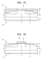
- FIG. 15 is a device cross-sectional view for illustrating the manufacturing method of the semiconductor device of the embodiment of the present invention, which is a device cross-sectional view of the portion corresponding to the unit periodic region T in the active cell of FIG. 3 in an individual manufacturing step (step of planarizing the gate polysilicon film).
- FIG. 16 is a device cross-sectional view for illustrating the manufacturing method of the semiconductor device of the embodiment of the present invention, which is a device cross-sectional view of the portion corresponding to the unit periodic region T in the active cell of FIG. 3 in an individual manufacturing step (step of removing the entire thick carbon film for high-temperature heat treatment).
- FIG. 16 is a device cross-sectional view for illustrating the manufacturing method of the semiconductor device of the embodiment of the present invention, which is a device cross-sectional view of the portion corresponding to the unit periodic region T in the active cell of FIG. 3 in an individual manufacturing step (step of removing the entire thick carbon film for high-temperature heat treatment).
- FIG. 17 is a device cross-sectional view for illustrating the manufacturing method of the semiconductor device of the embodiment of the present invention, which is a device cross-sectional view of the portion corresponding to the unit periodic region T in the active cell of FIG. 3 in an individual manufacturing step (step of forming a first-layer interlayer insulating film and a silicide film).
- FIG. 18 is a device cross-sectional view for illustrating the manufacturing method of the semiconductor device of the embodiment of the present invention, which is a device cross-sectional view of the portion corresponding to the unit periodic region T in the active cell of FIG. 3 in an individual manufacturing step (step of forming a first-layer surface metal film).
- FIG. 18 is a device cross-sectional view for illustrating the manufacturing method of the semiconductor device of the embodiment of the present invention, which is a device cross-sectional view of the portion corresponding to the unit periodic region T in the active cell of FIG. 3 in an individual manufacturing step (step of forming a first-layer surface metal film).
- FIG. 19 is a device cross-sectional view for illustrating the manufacturing method of the semiconductor device of the embodiment of the present invention, which is a device cross-sectional view of the portion corresponding to the unit periodic region T in the active cell of FIG. 3 in an individual manufacturing step (step of forming a second-layer surface metal film). Based on these drawings, a description will be given to a manufacturing process in the manufacturing method of the semiconductor device of the embodiment of the present invention.
- the N-type (first-conductivity-type) single-crystal SiC wafer 1 having a thickness of, e.g., about 700 micrometers (in a preferred range of, e.g., about 500 to 1000 micrometers) is prepared.
- the SiC wafer 1 has a resistivity of, e.g., about 20 m ⁇ cm.
- the SiC wafer 1 (the polytype of which is, e.g., 4H) has a diameter of, e.g., 76 mm (which may also be 100 mm, 150 mm, or a value other than those shown above).
- the crystal plane of the main surface e.g., a (0, 0, 0, 1) plane or a plane equivalent thereto is used.
- the SiC wafer 1 having a main orientation flat 31 and a sub-orientation flat 32 is used herein, though the use thereof is arbitrary.
- the crystal orientation is such that the direction of the main orientation flat 31 is, e.g., a [1, -1, 0, 0] direction, and a direction opposite to that of the sub-orientation flat 32 is, e.g., a [1, 1, -2, 0] direction.
- the N+ heavily doped drain layer 3 is formed.
- Preferred examples of ion implantation conditions include an ion species of, e.g., nitrogen, a dose of, e.g., about 5 x 10 14 /cm 2 , and an implantation energy of, e.g., about 50 KeV.
- activation annealing is performed (e.g., in an inert gas atmosphere at 1650 °C for about 3 minutes).
- the N- epitaxial layer 1e SiC epitaxial layer or first silicon-carbide-based semiconductor layer having a thickness of, e.g., about 5 to 10 micrometers
- a concentration range of an N-type impurity e.g., nitrogen
- examples of a concentration range of an N-type impurity include a range of about 1 x 10 16 /cm 3 to about 2 x 10 16 /cm 3 .
- a hard mask film 33 for introducing channel regions having a thickness of, e.g., about 2000 nm is deposited by, e.g., CVD (Chemical Vapor Deposition) using TEOS (Tetraethoxysilane) or the like.
- CVD Chemical Vapor Deposition
- TEOS Tetraethoxysilane
- a resist film 34 for introducing channel regions is coated and patterned by typical lithography.
- the silicon oxide film 33 is subjected to an anisotropic etching treatment using a fluorocarbon-based etching gas or the like to be patterned.
- the P-type channel regions 5 (P well regions, P base regions, or second-conductivity-type regions) are introduced into the surface region of the N- epitaxial layer 1e by ion implantation. That is, each of the following steps is performed. For instance, as preferred examples of conditions for the ion implantation, the following combinations (1) to (7) can be shown.
- the resist film 34 that is no longer needed is removed by ashing or the like.
- an insulating film 36 for forming dummy sidewalls each having a thickness of, e.g., about 200 nm is deposited by, e.g., CVD using TEOS or the like. Subsequently, by anisotropic dry etching, the insulating film 36 for forming dummy sidewalls is etched back to form dummy side walls 36.
- the N+ source regions 4 are introduced by ion implantation. That is, each of the following steps is performed. For instance, as preferred examples of conditions for the ion implantation, the following combinations (1) to (3) can be shown.
- a resist film 37 for introducing P+ contact regions is coated and patterned by normal lithography.
- the P+ contact regions 6 are introduced by ion implantation. That is, each of the following steps is performed. For instance, as preferred examples of conditions for the ion implantation, the following combinations (1) to (5) can be shown.
- the resist film 37 that is no longer needed is removed by ashing or the like.
- a thick carbon film 38 for high-temperature heat treatment having a thickness of, e.g., about 300 nm is deposited by CVD or the like.
- surface planarization is performed by, e.g., CMP (Chemical Mechanical Polishing) or the like. Thereafter, using a hydrofluoric-acid-based silicon-oxide-film etchant solution or the like, the dummy gate structure including the dummy gate 35 and the dummy sidewalls 36 is removed.
- CMP Chemical Mechanical Polishing
- a thin carbon film 39 for high-temperature heat treatment having a thickness of, e.g., about 100 nm is deposited by CVD or the like.
- activation annealing is performed.
- conditions for the activation annealing include a processing atmosphere of, e.g., an inert gas atmosphere, a processing temperature of, e.g., about 1800 °C, and a processing time of, e.g., about 1 minute.
- a processing atmosphere e.g., an inert gas atmosphere
- a processing temperature e.g., about 1800 °C
- a processing time e.g., about 1 minute.
- the thin carbon film 39 for high-temperature heat treatment is etched back to form a recessed portion 41 for buried gate (opening or opening pattern of the carbon film).
- the silicon oxide film-type gate insulating film 7 having a thickness of, e.g., about 50 nm is formed by, e.g., thermal oxidation or the like.
- a gate electrode polysilicon film 8 (gate electrode) having a thickness of, e.g., about 300 nm is deposited by CVD or the like.
- the gate electrode polysilicon film 8 e.g., a polysilicon film doped with phosphorus is preferred.
- surface planarization is performed by, e.g., CMP or the like.
- the gate electrode polysilicon film 8 is patterned into the gate electrode 8.
- the thick carbon film 38 for high-temperature heat treatment is removed.
- the patterning of the gate electrode polysilicon film 8 into the gate structure 30 (structure including the gate electrode 8, the gate insulating film 7, and the like) is completed.
- the first-layer interlayer insulating film 9 is deposited by CVD or the like. Subsequently, onto substantially the entire top surface 1a of the wafer 1, a resist film for forming contact holes is coated and patterned by normal lithography. Using the patterned resist film for forming contact holes as a mask, the contact holes 15 are formed in the first-layer interlayer insulating film 9 by anisotropic dry etching. Thereafter, the resist film for forming contact holes that is no longer needed is removed.
- a nickel film having a thickness of, e.g., about 50 nm is deposited by, e.g., sputtering deposition.
- a silicidation annealing treatment is performed at, e.g., 1000 °C for about 1 minute.
- unreacted nickel is removed by wet etching.
- a nickel film having a thickness of, e.g., about 50 nm is deposited by, e.g., sputtering deposition.
- a silicidation annealing treatment is performed at, e.g., 1000 °C for about 1 minute.
- the surface silicide films 10 are formed over the top surface 1a of the wafer 1, while the back-surface silicide film 11 is formed on the back surface 1b of the wafer 1.
- the tungsten plugs 20 are buried in the contact holes 15. Subsequently, over the first-layer interlayer insulating film 9, the first-layer surface metal films 16 (aluminum-based wiring films each having a thickness of, e.g., about 3000 nm) serving as the source lead-out metal wires 21 and the gate lead-out metal wire 19 are formed.
- the first-layer surface metal films 16 aluminum-based wiring films each having a thickness of, e.g., about 3000 nm serving as the source lead-out metal wires 21 and the gate lead-out metal wire 19 are formed.
- the second-layer interlayer insulating film 14 is deposited by CVD or the like. In the same manner as described above, the through holes are formed in the second-layer interlayer insulating film 14. Subsequently, over the second-layer interlayer insulating film 14, the second-layer surface metal film 17 (e.g., an aluminum-based wiring film having a thickness of about 3000 nm) coupled to the source lead-out metal wires 21 is formed and patterned to form the source metal electrode 18 (source pad). Thereafter, as necessary, a final passivation film such as, e.g., a polyimide film is deposited over the top surface 1a of the wafer 1 and patterned.
- a final passivation film such as, e.g., a polyimide film is deposited over the top surface 1a of the wafer 1 and patterned.
- the back-surface metal electrode film 12 (including, e.g., titanium/nickel/gold or like layers shown in order of increasing distance from the wafer 1) is formed by, e.g., sputtering. Thereafter, by dicing or the like, the wafer 1 is divided into the individual chips 2.
- This example is a variation of the example of Section 2 at the stage shown in FIGS. 13 to 19 . Accordingly, this example is exactly the same as the example of Section 2 at the stage shown in FIGS. 5 to 12 so that the description thereof will not be repeated.
- FIG. 20 is a device cross-sectional view for illustrating a manufacturing method of a semiconductor device (variation) of the embodiment of the present invention, which is a device cross-sectional view of the portion corresponding to the unit periodic region T in the active cell of FIG. 3 in an individual manufacturing step (step of enlarging the opening in the carbon film for high-temperature heat treatment).
- FIG. 21 is a device cross-sectional view for illustrating the manufacturing method of the semiconductor device (variation) of the embodiment of the present invention, which is a device cross-sectional view of the portion corresponding to the unit periodic region T in the active cell of FIG. 3 in an individual manufacturing step (step of forming the gate insulating film and the gate polysilicon film).
- FIG. 20 is a device cross-sectional view for illustrating a manufacturing method of a semiconductor device (variation) of the embodiment of the present invention, which is a device cross-sectional view of the portion corresponding to the unit periodic region T in the active cell of FIG. 3 in an individual manufacturing step (
- FIG. 22 is a device cross-sectional view for illustrating the manufacturing method of the semiconductor device (variation) of the embodiment of the present invention, which is a device cross-sectional view of the portion corresponding to the unit periodic region T in the active cell of FIG. 3 in an individual manufacturing step (step of planarizing the gate polysilicon film).
- FIG. 23 is a device cross-sectional view for illustrating the manufacturing method of the semiconductor device (variation) of the embodiment of the present invention, which is a device cross-sectional view of the portion corresponding to the unit periodic region T in the active cell of FIG. 3 in an individual manufacturing step (step of removing the entire thick carbon film for high-temperature heat treatment).
- FIG. 23 is a device cross-sectional view for illustrating the manufacturing method of the semiconductor device (variation) of the embodiment of the present invention, which is a device cross-sectional view of the portion corresponding to the unit periodic region T in the active cell of FIG. 3 in an individual manufacturing step (step of removing the entire thick carbon film for high-temperature
- FIG. 24 is a device cross-sectional view for illustrating the manufacturing method of the semiconductor device (variation) of the embodiment of the present invention, which is a device cross-sectional view of the portion corresponding to the unit periodic region T in the active cell of FIG. 3 in an individual manufacturing step (step of forming the first-layer interlayer insulating film and the silicide film).
- FIG. 25 is a device cross-sectional view for illustrating the manufacturing method of the semiconductor device (variation) of the embodiment of the present invention, which is a device cross-sectional view of the portion corresponding to the unit periodic region T in the active cell of FIG. 3 in an individual manufacturing step (step of forming the first-layer surface metal film).
- FIG. 24 is a device cross-sectional view for illustrating the manufacturing method of the semiconductor device (variation) of the embodiment of the present invention, which is a device cross-sectional view of the portion corresponding to the unit periodic region T in the active cell of FIG. 3 in an individual manufacturing step (step of forming the first-layer surface metal
- 26 is a device cross-sectional view for illustrating the manufacturing method of the semiconductor device (variation) of the embodiment of the present invention, which is a device cross-sectional view of the portion corresponding to the unit periodic region T in the active cell of FIG. 3 in an individual manufacturing step (step of forming the second-layer surface metal film). Based on these drawings, a description will be given to a variation of the manufacturing process in the manufacturing method of the semiconductor device of the embodiment of the present invention.
- the thin carbon film 39 for high-temperature heat treatment is etched back to form the recessed portion 41 for buried gate (opening or opening pattern of the carbon film).
- the thin carbon film 39 for high-temperature heat treatment is etched back to expose the top surface of the N-epitaxial layer 1e, but also the thick carbon film 38 for high-temperature heat treatment is caused to recede in a lateral direction (on both sides in the lateral direction) by a distance corresponding to the thickness of the CVD gate insulating film 7 described later.
- the alumina (aluminum-oxide) film-type gate insulating film 7 having a thickness of, e.g., about 50 nm is formed by, e.g., ALD (Atomic Layer Deposition) or the like.
- the gate electrode polysilicon film 8 (gate electrode) having a thickness of, e.g., about 300 nm is deposited by CVD or the like.
- the gate electrode polysilicon film 8 e.g., a polysilicon film doped with phosphorus is preferred.
- surface planarization is performed by, e.g., CMP or the like.
- the gate electrode polysilicon film 8 is patterned into the gate electrode 8.
- the thick carbon film 38 for high-temperature heat treatment is removed.
- the patterning of the gate electrode polysilicon film 8 into the gate structure 30 (structure including the gate electrode 8, the gate insulating film 7, and the like) is completed.
- the first-layer interlayer insulating film 9 is deposited by CVD or the like. Subsequently, onto substantially the entire top surface 1a of the wafer 1, a resist film for forming contact holes is coated and patterned by normal lithography. Using the patterned resist film for forming contact holes as a mask, the contact holes 15 are formed in the first-layer interlayer insulating film 9 by anisotropic dry etching. Thereafter, the resist film for forming contact holes that is no longer needed is removed.
- a nickel film having a thickness of, e.g., about 50 nm is deposited by, e.g., sputtering deposition.
- a silicidation annealing treatment is performed at, e.g., 1000 °C for about 1 minute.
- unreacted nickel is removed by wet etching.
- a nickel film having a thickness of, e.g., about 50 nm is deposited by, e.g., sputtering deposition.
- a silicidation annealing treatment is performed at, e.g., 1000 °C for about 1 minute.
- the surface silicide films 10 are formed over the top surface 1a of the wafer 1, while the back-surface silicide film 11 is formed on the back surface 1b of the wafer 1.
- the tungsten plugs 20 are buried in the contact holes 15. Subsequently, over the first-layer interlayer insulating film 9, the first-layer surface metal films 16 (aluminum-based wiring films each having a thickness of, e.g., about 3000 nm) serving as the source lead-out metal wires 21 and the gate lead-out metal wire 19 are formed.
- the first-layer surface metal films 16 aluminum-based wiring films each having a thickness of, e.g., about 3000 nm serving as the source lead-out metal wires 21 and the gate lead-out metal wire 19 are formed.
- the second-layer interlayer insulating film 14 is deposited by CVD or the like. In the same manner as described above, the through holes are formed in the second-layer interlayer insulating film 14. Subsequently, over the second-layer interlayer insulating film 14, the second-layer surface metal film 17 (e.g., an aluminum-based wiring film having a thickness of about 3000 nm) coupled to the source lead-out metal wires 21 is formed and patterned to form the source metal electrode 18 (source pad). Thereafter, as necessary, a final passivation film such as, e.g., a polyimide film is deposited over the top surface 1a of the wafer 1 and patterned.
- a final passivation film such as, e.g., a polyimide film is deposited over the top surface 1a of the wafer 1 and patterned.
- the back-surface metal electrode film 12 (including, e.g., titanium/nickel/gold or like layers shown in order of increasing distance from the wafer 1) is formed by, e.g., sputtering. Thereafter, by dicing or the like, the wafer 1 is divided into the individual chips 2.
- the edges of the P-type channel regions 5 are self-alignedly defined by the both edges of the dummy gate 35 (hard mask film 33 for introducing channel regions) (primary self alignment processing, i.e., dummy gate alignment processing).
- the edges of the N+ source regions 4 are defined at the both edges of the dummy sidewalls 36 (secondary self alignment processing, i.e., dummy sidewall alignment processing).
- the N+ source regions 4 are introduced in self-aligned relation with the P-type channel regions 5 (P well regions, P base regions, or second-conductivity-type regions).
- the self alignment is performed using the dummy sidewalls (or sidewalls).
- silicon-based insulating films silicon oxide films, silicon nitride films, or the like
- the both edges of the gate structure 30 are defined (ternary self-alignment processing, i.e., carbon film opening pattern alignment processing).
- the gate structure 30 (more specifically, the gate insulating film 7 and the gate electrode 8) is formed in self-aligned relation with the N+ source regions 4.
- self-alignment of the gate electrode 30 is performed using an opening pattern of a protective carbon film (reverse pattern of the protective carbon film) during activation annealing.
- Each of such self-alignment processings has the effect of facilitating high-precision control of device characteristics.
- activation annealing is normally performed at a temperature not less than a softening temperature of a silicon oxide film or the like. Therefore, a method which forms the gate structure 30 after activation annealing, i.e., a gate-last method is effective.
- the example of Section 3 is exactly the same as the example of Section 2 but, in FIG. 20 (corresponding to FIG. 13 in the example of Section 2), a correction corresponding to the thickness of the gate insulating film 7 is made in the gate structure 30 so as to define the both edges of the gate electrode 8.
- the both edges of the gate electrode 8 coincide with those of the gate insulating film 7 while, in the example of Section 3, the edges of the gate electrode 8 and the gate insulating film 7 are each shifted by a distance corresponding to the thickness of the gate insulating film 7 on both sides of the gate electrode 8.
- the gate insulating film 7 is deposited by practicing a foreign method such as CVD or sputtering deposition.
- a foreign method such as CVD or sputtering deposition.
- any film can be deposited independently of the characteristics of the underlie, i.e., SiC. Therefore, it is possible to achieve stable insulating film characteristics and a relatively high channel mobility. That is, when consideration is given to the fact that, in a silicon-carbide-based device, improving the characteristics of a thermal oxide film has become a challenge to be met due to the presence of carbon atoms, as far as such a challenge is concerned, it is more advantageous to use a foreign insulating film than a thermally oxidized gate insulating film.
- the specific description has been given mainly to the N-channel power MISFET, but the present invention is not limited thereto. It will be appreciated that the present invention is also applicable to a P-channel power MISFET. Also, in the foregoing embodiment, the specific description has been given mainly to an active device (such as FET, IGBT, or diode) using a silicon-carbide-based semiconductor substrate (the polytype of which is not limited to 4H, and may also be another) of SiC or the like, but the present invention is not limited thereto. It will be appreciated that the present invention is also applicable to a GaN-based active device. Also, in the foregoing embodiment, the specific description has been given mainly to the planar type, but the present invention is not limited thereto. It will be appreciated that the present invention is also similarly applicable to the trench type.
Landscapes
- Engineering & Computer Science (AREA)
- Microelectronics & Electronic Packaging (AREA)
- Power Engineering (AREA)
- Condensed Matter Physics & Semiconductors (AREA)
- General Physics & Mathematics (AREA)
- Physics & Mathematics (AREA)
- Ceramic Engineering (AREA)
- Computer Hardware Design (AREA)
- Chemical & Material Sciences (AREA)
- Crystallography & Structural Chemistry (AREA)
- Manufacturing & Machinery (AREA)
- Electrodes Of Semiconductors (AREA)
- Insulated Gate Type Field-Effect Transistor (AREA)
- Metal-Oxide And Bipolar Metal-Oxide Semiconductor Integrated Circuits (AREA)
Abstract
Description
- The disclosure of Japanese Patent Application No.
2011-17595 - The present invention relates to a technology which is effective when applied to a self-alignment technique in a semiconductor device (or semiconductor integrated circuit device) such as a MOSFET (Metal Oxide Semiconductor Field Effect Transistor) or MISFET (Metal Insulator Semiconductor Field Effect Transistor) and a manufacturing method thereof.
- Japanese Unexamined Patent Publication No.
2008-108869 - Japanese Unexamined Patent Publication No.
2008-147576 US Patent Publication No. 2010-35420 (Patent Document 3) corresponding thereto discloses a technique in which, with regard to a manufacturing method of a SiC-semiconductor-based vertical N-channel MOSFET or MISFET, the width of a tungsten hard mask is reduced to form source regions and channel regions by self alignment. The publication also discloses a technique in which, after a heat treatment for the source regions and the channel regions, a gate structure is formed. -
- [Patent Document 1]
Japanese Unexamined Patent Publication No.2008-108869 - [Patent Document 2]
Japanese Unexamined Patent Publication No.2008-147576 - [Patent Document 3]
US Patent Publication No. 2010-35420 - In a SiC-based MISFET manufacturing process, after the introduction of an impurity, extremely-high-temperature activation annealing is required. Accordingly, it is difficult to frequently use a self-alignment process as performed in a silicon-based MISFET manufacturing process. This results in the problem that, to control the characteristics of a device, a high-accuracy alignment technique is indispensable.
- The present invention has been achieved in the light of such a problem.
- A preferred aim of the present invention is to provide a semiconductor device and a manufacturing process thereof which allow frequent use of a self-alignment technique.
- The above and other aims and novel features of the present invention will become apparent from a statement in the present specification and the accompanying drawings.
- The following is a brief description of the outline of a representative embodiment of the invention disclosed in the present application.
- That is, according to an aspect of the present invention, in a semiconductor device such as a SiC-based vertical power MISFET using a silicon-carbide-based semiconductor substrate and a manufacturing method thereof, a channel region, a source region, and a gate structure are formed in mutually self-aligned relation.
- The following is a brief description of an effect obtained according to the representative embodiment of the invention disclosed in the present application.
- That is, in a semiconductor device such as a SiC-based vertical power MISFET using a silicon-carbide-based semiconductor substrate and a manufacturing method thereof, a channel region, a source region, and a gate structure are formed in mutually self-aligned relation. This allows precise control of the characteristics of a device to be performed relatively easily.
- In the drawings
-
FIG. 1 is a top view of an example of a target device chip in a manufacturing method of a semiconductor device of an embodiment of the present invention; -
FIG. 2 is an enlarged top view of two periods of a unit periodic region T in the active cell ofFIG. 1 ; -
FIG. 3 is a device cross-sectional view corresponding to the X-X' cross section ofFIG. 2 ; -
FIG. 4 is an overall top view of a single-crystal SiC wafer (epitaxial wafer) used in the manufacturing method of the semiconductor device of the embodiment of the present invention; -
FIG. 5 is a device cross-sectional view for illustrating the manufacturing method of the semiconductor device of the embodiment of the present invention, which is a device cross-sectional view of a portion corresponding to the unit periodic region T in the active cell ofFIG. 3 in an individual manufacturing step (step of forming a hard mask for introducing channel regions); -
FIG. 6 is a device cross-sectional view for illustrating the manufacturing method of the semiconductor device of the embodiment of the present invention, which is a device cross-sectional view of the portion corresponding to the unit periodic region T in the active cell ofFIG. 3 in an individual manufacturing step (step of introducing the channel regions); -
FIG. 7 is a device cross-sectional view for illustrating the manufacturing method of the semiconductor device of the embodiment of the present invention, which is a device cross-sectional view of the portion corresponding to the unit periodic region T in the active cell ofFIG. 3 in an individual manufacturing step (step of forming sidewalls); -
FIG. 8 is a device cross-sectional view for illustrating the manufacturing method of the semiconductor device of the embodiment of the present invention, which is a device cross-sectional view of the portion corresponding to the unit periodic region T in the active cell ofFIG. 3 in an individual manufacturing step (step of introducing N+ source regions); -
FIG. 9 is a device cross-sectional view for illustrating the manufacturing method of the semiconductor device of the embodiment of the present invention, which is a device cross-sectional view of the portion corresponding to the unit periodic region T in the active cell ofFIG. 3 in an individual manufacturing step (step of introducing P+ contact regions); -
FIG. 10 is a device cross-sectional view for illustrating the manufacturing method of the semiconductor device of the embodiment of the present invention, which is a device cross-sectional view of the portion corresponding to the unit periodic region T in the active cell ofFIG. 3 in an individual manufacturing step (step of forming a thick carbon film for high-temperature heat treatment); -
FIG. 11 is a device cross-sectional view for illustrating the manufacturing method of the semiconductor device of the embodiment of the present invention, which is a device cross-sectional view of the portion corresponding to the unit periodic region T in the active cell ofFIG. 3 in an individual manufacturing step (step of planarizing the thick carbon film for high-temperature heat treatment); -
FIG. 12 is a device cross-sectional view for illustrating the manufacturing method of the semiconductor device of the embodiment of the present invention, which is a device cross-sectional view of the portion corresponding to the unit periodic region T in the active cell ofFIG. 3 in an individual manufacturing step (step of forming a thin carbon film for high-temperature heat treatment); -
FIG. 13 is a device cross-sectional view for illustrating the manufacturing method of the semiconductor device of the embodiment of the present invention, which is a device cross-sectional view of the portion corresponding to the unit periodic region T in the active cell ofFIG. 3 in an individual manufacturing step (step of removing the thin carbon film for high-temperature heat treatment); -
FIG. 14 is a device cross-sectional view for illustrating the manufacturing method of the semiconductor device of the embodiment of the present invention, which is a device cross-sectional view of the portion corresponding to the unit periodic region T in the active cell ofFIG. 3 in an individual manufacturing step (step of forming a gate insulating film and a gate polysilicon film); -
FIG. 15 is a device cross-sectional view for illustrating the manufacturing method of the semiconductor device of the embodiment of the present invention, which is a device cross-sectional view of the portion corresponding to the unit periodic region T in the active cell ofFIG. 3 in an individual manufacturing step (step of planarizing the gate polysilicon film); -
FIG. 16 is a device cross-sectional view for illustrating the manufacturing method of the semiconductor device of the embodiment of the present invention, which is a device cross-sectional view of the portion corresponding to the unit periodic region T in the active cell ofFIG. 3 in an individual manufacturing step (step of removing the entire thick carbon film for high-temperature heat treatment); -
FIG. 17 is a device cross-sectional view for illustrating the manufacturing method of the semiconductor device of the embodiment of the present invention, which is a device cross-sectional view of the portion corresponding to the unit periodic region T in the active cell ofFIG. 3 in an individual manufacturing step (step of forming a first-layer interlayer insulating film and a silicide film); -
FIG. 18 is a device cross-sectional view for illustrating the manufacturing method of the semiconductor device of the embodiment of the present invention, which is a device cross-sectional view of the portion corresponding to the unit periodic region T in the active cell ofFIG. 3 in an individual manufacturing step (step of forming a first-layer surface metal film); -
FIG. 19 is a device cross-sectional view for illustrating the manufacturing method of the semiconductor device of the embodiment of the present invention, which is a device cross-sectional view of the portion corresponding to the unit periodic region T in the active cell ofFIG. 3 in an individual manufacturing step (step of forming a second-layer surface metal film); -
FIG. 20 is a device cross-sectional view for illustrating a manufacturing method of a semiconductor device (variation) of the embodiment of the present invention, which is a device cross-sectional view of the portion corresponding to the unit periodic region T in the active cell ofFIG. 3 in an individual manufacturing step (step of enlarging the opening in the carbon film for high-temperature heat treatment); -
FIG. 21 is a device cross-sectional view for illustrating the manufacturing method of the semiconductor device (variation) of the embodiment of the present invention, which is a device cross-sectional view of the portion corresponding to the unit periodic region T in the active cell ofFIG. 3 in an individual manufacturing step (step of forming the gate insulating film and the gate polysilicon film); -
FIG. 22 is a device cross-sectional view for illustrating the manufacturing method of the semiconductor device (variation) of the embodiment of the present invention, which is a device cross-sectional view of the portion corresponding to the unit periodic region T in the active cell ofFIG. 3 in an individual manufacturing step (step of planarizing the gate polysilicon film); -
FIG. 23 is a device cross-sectional view for illustrating the manufacturing method of the semiconductor device (variation) of the embodiment of the present invention, which is a device cross-sectional view of the portion corresponding to the unit periodic region T in the active cell ofFIG. 3 in an individual manufacturing step (step of removing the entire thick carbon film for high-temperature heat treatment); -
FIG. 24 is a device cross-sectional view for illustrating the manufacturing method of the semiconductor device (variation) of the embodiment of the present invention, which is a device cross-sectional view of the portion corresponding to the unit periodic region T in the active cell ofFIG. 3 in an individual manufacturing step (step of forming the first-layer interlayer insulating film and the silicide film); -
FIG. 25 is a device cross-sectional view for illustrating the manufacturing method of the semiconductor device (variation) of the embodiment of the present invention, which is a device cross-sectional view of the portion corresponding to the unit periodic region T in the active cell ofFIG. 3 in an individual manufacturing step (step of forming the first-layer surface metal film); and -
FIG. 26 is a device cross-sectional view for illustrating the manufacturing method of the semiconductor device (variation) of the embodiment of the present invention, which is a device cross-sectional view of the portion corresponding to the unit periodic region T in the active cell ofFIG. 3 in an individual manufacturing step (step of forming the second-layer surface metal film). - First, a description will be given to the outline of a representative embodiment of the invention disclosed in the present application.
- 1. A method of manufacturing a semiconductor device includes the steps of: (a) preparing a semiconductor wafer having, in a first main surface of a silicon-carbide-based semiconductor substrate having a first conductivity type, a first silicon-carbide-based semiconductor layer having the same conductivity type as the first conductivity type and a concentration lower than that of the semiconductor substrate; (b) introducing, into a surface region of the first silicon-carbide-based semiconductor layer closer to the first main surface, a second-conductivity-type region having a second conductivity type opposite to the first conductivity type and serving as a channel region of a vertical power MISFET; (c) introducing a source region of the vertical power MISFET having the same conductivity type as the first conductivity type and a concentration higher than that of the first silicon-carbide-based semiconductor layer in self-aligned relation with the second-conductivity-type region; and (d) forming a gate structure of the vertical power MISFET in self-aligned relation with the source region.
- 2. In the method of manufacturing a semiconductor device according to
article 1, the first silicon-carbide-based semiconductor layer is an epitaxial layer. - 3. The method of manufacturing a semiconductor device according to
article - 4. In the method of manufacturing a semiconductor device according to any one of
articles 1 to 3, self-alignment of the source region with the second-conductivity-type region is performed using sidewalls each formed of a silicon-based insulating film. - 5. In the method of manufacturing a semiconductor device according to any one of
articles 1 to 4, self-alignment of the gate structure with the source region is performed using an opening pattern of a carbon film. - 6. In the method of manufacturing a semiconductor device according to any one of
articles 1 to 5, the semiconductor substrate is of an N-type. - 7. In the method of manufacturing a semiconductor device according to any one of
articles 1 to 6, the first silicon-carbide-based semiconductor layer is of the N-type. - 8. In the method of manufacturing a semiconductor device according to any one of
articles 1 to 7, a gate insulating film forming the gate structure is a thermal oxide film. - 9. In the method of manufacturing a semiconductor device according to any one of
articles 1 to 7, a gate insulating film forming the gate structure is an insulating film deposited by CVD. - 10. In the method of manufacturing a semiconductor device according to
article 9, the CVD is ALD. - 11. In the method of manufacturing a semiconductor device according to
article - 12. The method of manufacturing a semiconductor device according to any one of
articles 9 to 11 further includes the step of: (f) after the step (e) and prior to the step (d), enlarging the opening pattern of the carbon film by a dimension substantially equal to a thickness of the gate insulating film. - 13. In the method of manufacturing a semiconductor device according to any one of
articles 1 to 12, a polytype of the semiconductor substrate is 4H. - 14. In the method of manufacturing a semiconductor device according to any one of
articles 1 to 13, the first main surface of the semiconductor substrate is a (0001) plane or a plane equivalent thereto. - 15. A method of manufacturing a semiconductor device includes the steps of: (a) preparing a semiconductor wafer having, in a first main surface of a silicon-carbide-based semiconductor substrate having a first conductivity type, a first silicon-carbide-based semiconductor layer having the same conductivity type as the first conductivity type and a concentration lower than that of the semiconductor substrate; (b) introducing, into a surface region of the first silicon-carbide-based semiconductor layer closer to the first main surface, a second-conductivity-type region having a second conductivity type opposite to the first conductivity type and serving as a channel region of a vertical power MISFET; (c) introducing a source region of the vertical power MISFET having the same conductivity type as the first conductivity type and a concentration higher than that of the first silicon-carbide-based semiconductor layer in self-aligned relation with the second-conductivity-type region; (d) performing an activation anneal treatment for the second-conductivity-type region and the source region; and (e) after the step (d), forming a gate structure of the vertical power MISFET. In the method of manufacturing a semiconductor device, self-alignment of the source region with the second-conductivity-type region is performed using sidewalls each formed of a silicon-based insulating film.
- 16. In the method of manufacturing a semiconductor device according to
article 15, the first silicon-carbide-based semiconductor layer is an epitaxial layer. - 17. In the method of manufacturing a semiconductor device according to
article - 18. In the method of manufacturing a semiconductor device according to any one of
articles 15 to 17, the first silicon-carbide-based semiconductor layer is of the N-type. - 19. In the method of manufacturing a semiconductor device according to any one of
articles 15 to 18, a gate insulating film forming the gate structure is a thermal oxide film. - 20. In the method of manufacturing a semiconductor device according to any one of
articles 15 to 18, a gate insulating film forming the gate structure is an insulating film deposited by CVD. - 21. In the method of manufacturing a semiconductor device according to
article 20, the CVD is ALD. - 22. In the method of manufacturing a semiconductor
device according article 21, the gate insulating film forming the gate structure has an alumina-based insulating film. - 23. In the method of manufacturing a semiconductor device according to any one of
articles 15 to 22, a polytype of the semiconductor substrate is 4H. - 24. In the method of manufacturing a semiconductor device according to any one of
articles 15 to 23, the first main surface of the semiconductor substrate is a (0001) plane or a plane equivalent thereto. - 25. A semiconductor device includes: a silicon-carbide-based semiconductor substrate having a first main surface having a first conductivity type, the silicon-carbide-based semiconductor substrate including: a first silicon-carbide-based semiconductor layer having the same conductivity type as the first conductivity type and a concentration lower than that of the silicon carbide-based semiconductor substrate; a channel region having a second conductivity type and formed in a surface region of the first silicon-carbide-based semiconductor layer closer to the first main surface; a source region having the first conductivity type and a concentration higher than that of the first silicon-carbide-based semiconductor layer and formed in self-aligned relation with the channel region; and a gate structure formed in self-aligned relation with the source region.
- 26. In the semiconductor device according to article 25, the semiconductor device is a vertical MISFET.
- 27. In the semiconductor device according to article 25 or 26, the first silicon-carbide-based semiconductor layer is an epitaxial layer.
- 28. In the semiconductor device according to any one of articles 25 to 27, self-alignment of the source region with the second-conductivity-type region is performed using sidewalls each formed of a silicon-based insulating film.
- 29. In the semiconductor device according to any one of articles 25 to 28, self-alignment of the gate structure with the source region is performed using an opening pattern of a carbon film.
-
- 1. In the present application, if necessary for the sake of convenience, the description of an embodiment may be such that the embodiment is divided into a plurality of sections in the description thereof. However, they are by no means independent of or distinct from each other unless particularly explicitly described otherwise, and one of the individual sections of a single example is details, variations, and so forth of part or the whole of the others. In principle, a repeated description of like parts will be omitted. Each constituent element in the embodiment is not indispensable unless particularly explicitly described otherwise, unless the constituent element is theoretically limited to a given number, or unless it is obvious from the context that the constituent element is indispensable.
- Also in the present application, when a "semiconductor chip", "semiconductor device", or "semiconductor integrated circuit device" is mentioned, it primarily refers to various stand-alone transistors (active elements) and to a device in which a resistor, a capacitor, a diode, and the like are integrated around such a stand-alone transistor over a semiconductor chip or the like (examples of a material for the semiconductor chip include a single-crystal SiC substrate, a single-crystal silicon substrate, a composite substrate thereof, and the like. As a crystal polymorph of SiC, 4H-SiC is primarily referred to, but it will be appreciated that another crystal polymorph may also be referred to).
- In the present application, when an "electronic circuit device" is mentioned, it indicates a semiconductor chip, a semiconductor device, a semiconductor integrated circuit device, a resistor, a capacitor, a diode, or the like and an interconnected system thereof.
- Here, representative examples of the various transistors that can be shown include a MISFET. By forming a large number of the MISFETs in parallel to allow handling of high power, a power MISFET is obtained. Power MISFETs include a vertical MISFET and a lateral MISFET. In the present application, a specific description will be given mainly to the vertical MISFET. Such vertical MISFETs include a Planar type and a Trench type. In the present application, a specific description will be given mainly to the planar type.
- In these days, each of the source and gate metal electrodes of a power-type electronic circuit device, semiconductor device, or semiconductor integrated circuit device is normally and mostly formed of one layer which is, e.g., an aluminum-based (or refractory-metal-based, e.g., tungsten-based) wiring layer M1 or two layers which are aluminum-based (or refractory-metal-based, e.g., tungsten-based) wiring layers M1 and M2. Note that, as such wiring layers, copper-based wiring layers are used occasionally.
- 2. Likewise, even when such wording as "X comprised of A" is used in association with a material, a composition, or the like in the description of the embodiment or the like, it does not exclude a material, a composition, or the like which contains an element other than A as one of the main constituent elements thereof unless particularly explicitly described otherwise or unless it is obvious from the context that it excludes such a material, composition, or the like. For example, when a component is mentioned, the wording means "X containing A as a main component" or the like. It will be appreciated that, even when, e.g., a "silicon member", "SiC (silicon carbide) member", or the like is mentioned, it is not limited to pure silicon or SiC, and a member containing a multi-element semiconductor containing silicon or SiC as a main component, another additive, or the like is also included. Likewise, it will also be appreciated that, even when a "silicon oxide film", "silicon-oxide-based insulating film", or the like is mentioned, it includes not only a relatively pure Undoped Silicon Dioxide, but also a thermal oxide film of FSG (Fluorosilicate Glass), TEOS-based silicon oxide, SiOC (Silicon Oxicarbide), Carbon-doped Silicon oxide, OSG (Organosilicate glass), PSG (Phosphorus Silicate Glass), BPSG (Borophosphosilicate Glass), or the like, a CVD oxide film, a coated silicon oxide such as SOG (Spin ON Glass) or NCS (Nano-Clustering Silica), a silica-based Low-k insulating film (porous insulating film) obtained by introducing voids into the same member as mentioned above, a composite film with another silicon-based insulating film which contains any of these mentioned above as a main constituent element thereof, and the like.
- As a silicon-based insulating film commonly used in a semiconductor field along with a silicon-oxide-based insulating film, there is a silicon-nitride-based insulating film. Materials belonging to this system include SiN, SiCN, SiNH, SiCNH, and the like. Here, when "silicon nitride" is mentioned, it includes both of SiN and SiNH unless particularly explicitly described otherwise. Likewise, when "SiCN" is mentioned, it includes both of SiCN and SiCNH unless particularly explicitly described otherwise.
- 3. Likewise, it will also be appreciated that, although a preferred example is shown in association with a graphical figure, a position, an attribute, or the like, the graphical figure, position, attribute, or the like is not strictly limited thereto unless particularly explicitly described otherwise or unless it is obvious from the context that the graphical figure, position, attribute, or the like is strictly limited thereto.
- 4. Further, when a specific numerical value or numerical amount is mentioned, it may be a value more or less than the specific numerical value unless particularly explicitly described otherwise, unless the numerical value is theoretically limited to a given number, or unless it is obvious from the context that the numeral value is limited to a given number.
- 5. When a "wafer" is mentioned, it typically refers to a single-crystal silicon carbide wafer, a single-crystal silicon wafer, or the like over which a semiconductor integrated circuit device (the same as a semiconductor device or an electronic device) is formed. However, it will be appreciated that the "wafer" also includes a composite wafer of an insulating substrate and a semiconductor layer or the like, such as an epitaxial wafer or an LCD glass substrate.
- 6. In the present application, when an "ordinary temperature" or "room temperature" is mentioned, it commonly refers to a temperature of, e.g., about 25 °C or a range of, e.g., about 15 °C to about 35 °C.
- In the present application, when the wording "A is formed in self-aligned relation with B" is used, it shows that B is formed substantially in alignment with A without performing a special alignment step for aligning B with A. Also, when the wording "A, B, and C are in mutually self-aligned relation" is used, it shows that one of at least two of A, B, and C are in self-aligned relation with the remaining one, while the other of the two is in self-aligned relation with the remaining one or the one of the two.
- In the present application, a "gate structure" refers to a structure including a gate insulating film, a gate electrode (a portion actually functioning as a gate, such as a polysilicon gate electrode), and the like. Therefore, an upper-layer metal gate electrode and the like are excluded therefrom.
- An embodiment will be described in greater detail. In each of the drawings, the same or like parts are designated by the same or similar marks or reference numerals, and a description thereof will not be repeated in principle.
- In the accompanying drawings, hatching or the like may be omitted even in a cross section when hatching or the like results in complicated illustration or when the distinction between a portion to be hatched and a vacant space is distinct. In relation thereto, even a two-dimensionally closed hole may have a background outline thereof omitted when it is obvious from the description or the like that the hole is two-dimensionally closed, and so forth. On the other hand, even though not shown in a cross section, a portion other than a vacant space may be hatched to clearly show that the hatched portion is not a vacant space.
- Note that, here, to give a specific description, a device having a source/drain breakdown voltage of about 800 to 1000 V is assumed and described.
-
FIG. 1 is a top view of an example of a target device chip in the manufacturing method of the semiconductor device of the embodiment of the present invention.FIG. 2 is an enlarged top view of two periods of a unit periodic region T in the active cell ofFIG. 1 .FIG. 3 is a device cross-sectional view corresponding to the X-Xʹ cross section ofFIG. 2 . Based on these drawings, a description will be given to an example of a structure of the target device in the manufacturing method of the semiconductor device of the embodiment of the present invention. - First,
FIG. 1 shows an upper-surface overall view of an example of atarget device chip 2 in the manufacturing method of the semiconductor device of the embodiment of the present invention. As shown inFIG. 1 , in the vicinity of the outer periphery of atop surface 1a (first main surface) of asemiconductor chip 2, a gate metal electrode 24 (including a gate pad) is provided while, in the middle portion thereof, anactive cell region 22 is provided. Theactive cell region 22 includes a large number of the unit periodic regions T and the like. The upper surface of theactive cell region 22 and the periphery thereof are covered with a source metal electrode 18 (including a source pad). Around theactive cell region 22, a ring-like P+edge termination area 23 is provided so as to surround theactive cell region 22. Note that the P+edge termination area 23 is formed simultaneously with, e.g., P-type channel regions 5 (P well regions, P base regions, or second-conductivity-type regions) described later usingFIG. 2 or the like. - Based on
FIGS. 2 and3 , a detailed structure of each of the unit periodic regions T will be described. As shown inFIG. 2 or3 , in theback surface 1b of an N-type substrate 1s (first-conductivity-type substrate) of thesemiconductor chip 2, anN+ drain region 3 is provided and, over the chip backsurface 1b, a back-surfacemetal electrode film 12 is provided via a back-surface silicide film 11. In thetop surface 1a of the N-type substrate 1s (first-conductivity-type substrate), an N-epitaxial layer 1e (SiC epitaxial layer or first silicon-carbide-based semiconductor layer) forming a drift region is provided. In the surface region of the N-epitaxial layer 1e, the P-type channel regions 5 (P well regions, P base regions, or second-conductivity-type regions) are provided. In the surface regions of the P-type channel regions 5,N+ source regions 4 andP+ contact regions 6 are provided. Over the top surface of the N-epitaxial layer 1e, gate electrodes 8 (or gate electrode polysilicon films) are formed viagate insulating films 7, and a first-layerinterlayer insulating film 9 is formed so as to coversuch gate structures 30. In contact holes 15 provided in the first-layerinterlayer insulating film 9, tungsten plugs 20 are provided viasurface silicide films 10. Over the upper surface of the first-layerinterlayer insulating film 9, source lead-outmetal wires 21 and gate lead-outmetal wires 19 which are formed of first-layersurface metal films 16 are formed. Further, over the upper surface of the first-layerinterlayer insulating film 9, a second-layerinterlayer insulating film 14 is formed so as to cover the first-layersurface metal films 16. Over the second-layerinterlayer insulating film 14, a source metal electrode 18 (source pad) formed of a second-layersurface metal film 17 coupled to the source lead-outmetal wires 21 via through holes is formed. - In the following process, a wafer temperature in ion implantation is, e.g., about 400 °C (relatively high temperature) when an ion species is nitrogen, but ion implantation is performed at, e.g., an ordinary temperature or a room temperature when an ion species is other than nitrogen. Note that the temperatures mentioned above are only exemplary, and temperatures (higher temperatures or a cooled state under 15 °C) other than those mentioned above are not to be excluded.
-
FIG. 4 is an overall top view of a single-crystal SiC wafer (epitaxial wafer) used in the manufacturing method of the semiconductor device of the embodiment of the present invention.FIG. 5 is a device cross-sectional view for illustrating the manufacturing method of the semiconductor device of the embodiment of the present invention, which is a device cross-sectional view of a portion corresponding to the unit periodic region T in the active cell ofFIG. 3 in an individual manufacturing step (step of forming a hard mask for introducing channel regions).FIG. 6 is a device cross-sectional view for illustrating the manufacturing method of the semiconductor device of the embodiment of the present invention, which is a device cross-sectional view of the portion corresponding to the unit periodic region T in the active cell ofFIG. 3 in an individual manufacturing step (step of introducing the channel regions).FIG. 7 is a device cross-sectional view for illustrating the manufacturing method of the semiconductor device of the embodiment of the present invention, which is a device cross-sectional view of the portion corresponding to the unit periodic region T in the active cell ofFIG. 3 in an individual manufacturing step (step of forming sidewalls).FIG. 8 is a device cross-sectional view for illustrating the manufacturing method of the semiconductor device of the embodiment of the present invention, which is a device cross-sectional view of the portion corresponding to the unit periodic region T in the active cell ofFIG. 3 in an individual manufacturing step (step of introducing N+ source regions).FIG. 9 is a device cross-sectional view for illustrating the manufacturing method of the semiconductor device of the embodiment of the present invention, which is a device cross-sectional view of the portion corresponding to the unit periodic region T in the active cell ofFIG. 3 in an individual manufacturing step (step of introducing P+ contact regions).FIG. 10 is a device cross-sectional view for illustrating the manufacturing method of the semiconductor device of the embodiment of the present invention, which is a device cross-sectional view of the portion corresponding to the unit periodic region T in the active cell ofFIG. 3 in an individual manufacturing step (step of forming a thick carbon film for high-temperature heat treatment).FIG. 11 is a device cross-sectional view for illustrating the manufacturing method of the semiconductor device of the embodiment of the present invention, which is a device cross-sectional view of the portion corresponding to the unit periodic region T in the active cell ofFIG. 3 in an individual manufacturing step (step of planarizing the thick carbon film for high-temperature heat treatment).FIG. 12 is a device cross-sectional view for illustrating the manufacturing method of the semiconductor device of the embodiment of the present invention, which is a device cross-sectional view of the portion corresponding to the unit periodic region T in the active cell ofFIG. 3 in an individual manufacturing step (step of forming a thin carbon film for high-temperature heat treatment).FIG. 13 is a device cross-sectional view for illustrating the manufacturing method of the semiconductor device of the embodiment of the present invention, which is a device cross-sectional view of the portion corresponding to the unit periodic region T in the active cell ofFIG. 3 in an individual manufacturing step (step of removing the thin carbon film for high-temperature heat treatment).FIG. 14 is a device cross-sectional view for illustrating the manufacturing method of the semiconductor device of the embodiment of the present invention, which is a device cross-sectional view of the portion corresponding to the unit periodic region T in the active cell ofFIG. 3 in an individual manufacturing step (step of forming a gate insulating film and a gate polysilicon film).FIG. 15 is a device cross-sectional view for illustrating the manufacturing method of the semiconductor device of the embodiment of the present invention, which is a device cross-sectional view of the portion corresponding to the unit periodic region T in the active cell ofFIG. 3 in an individual manufacturing step (step of planarizing the gate polysilicon film).FIG. 16 is a device cross-sectional view for illustrating the manufacturing method of the semiconductor device of the embodiment of the present invention, which is a device cross-sectional view of the portion corresponding to the unit periodic region T in the active cell ofFIG. 3 in an individual manufacturing step (step of removing the entire thick carbon film for high-temperature heat treatment).FIG. 17 is a device cross-sectional view for illustrating the manufacturing method of the semiconductor device of the embodiment of the present invention, which is a device cross-sectional view of the portion corresponding to the unit periodic region T in the active cell ofFIG. 3 in an individual manufacturing step (step of forming a first-layer interlayer insulating film and a silicide film).FIG. 18 is a device cross-sectional view for illustrating the manufacturing method of the semiconductor device of the embodiment of the present invention, which is a device cross-sectional view of the portion corresponding to the unit periodic region T in the active cell ofFIG. 3 in an individual manufacturing step (step of forming a first-layer surface metal film).FIG. 19 is a device cross-sectional view for illustrating the manufacturing method of the semiconductor device of the embodiment of the present invention, which is a device cross-sectional view of the portion corresponding to the unit periodic region T in the active cell ofFIG. 3 in an individual manufacturing step (step of forming a second-layer surface metal film). Based on these drawings, a description will be given to a manufacturing process in the manufacturing method of the semiconductor device of the embodiment of the present invention. - First, as shown in
FIG. 4 , the N-type (first-conductivity-type) single-crystal SiC wafer 1 having a thickness of, e.g., about 700 micrometers (in a preferred range of, e.g., about 500 to 1000 micrometers) is prepared. TheSiC wafer 1 has a resistivity of, e.g., about 20 mΩ·cm. The SiC wafer 1 (the polytype of which is, e.g., 4H) has a diameter of, e.g., 76 mm (which may also be 100 mm, 150 mm, or a value other than those shown above). As the crystal plane of the main surface, e.g., a (0, 0, 0, 1) plane or a plane equivalent thereto is used. Note that theSiC wafer 1 having a main orientation flat 31 and a sub-orientation flat 32 is used herein, though the use thereof is arbitrary. The crystal orientation is such that the direction of the main orientation flat 31 is, e.g., a [1, -1, 0, 0] direction, and a direction opposite to that of the sub-orientation flat 32 is, e.g., a [1, 1, -2, 0] direction. - Next, as shown in
FIG. 5 , by introducing an N-type impurity from theback surface 1b of thewafer 1 by, e.g., ion implantation, the N+ heavily dopeddrain layer 3 is formed. Preferred examples of ion implantation conditions that can be shown include an ion species of, e.g., nitrogen, a dose of, e.g., about 5 x 10¹⁴/cm2, and an implantation energy of, e.g., about 50 KeV. Thereafter, activation annealing is performed (e.g., in an inert gas atmosphere at 1650 °C for about 3 minutes). - Next, in substantially the entire
top surface 1a of thewafer 1, the N-epitaxial layer 1e (SiC epitaxial layer or first silicon-carbide-based semiconductor layer) having a thickness of, e.g., about 5 to 10 micrometers) in accordance with a required breakdown voltage is formed by vapor-phase epitaxial growth. Examples of a concentration range of an N-type impurity (e.g., nitrogen) that can be shown include a range of about 1 x 10¹⁶/cm3 to about 2 x 10¹⁶/cm3. - Next, over substantially the entire
top surface 1a of thewafer 1, ahard mask film 33 for introducing channel regions having a thickness of, e.g., about 2000 nm is deposited by, e.g., CVD (Chemical Vapor Deposition) using TEOS (Tetraethoxysilane) or the like. Subsequently, onto thehard mask 33 for introducing channel regions, a resistfilm 34 for introducing channel regions is coated and patterned by typical lithography. Subsequently, using the patterned resistfilm 34 as a mask, thesilicon oxide film 33 is subjected to an anisotropic etching treatment using a fluorocarbon-based etching gas or the like to be patterned. - Next, as shown in
FIG. 6 , using thehard mask film 33 for introducing channel regions as a mask for ion implantation, the P-type channel regions 5 (P well regions, P base regions, or second-conductivity-type regions) are introduced into the surface region of the N-epitaxial layer 1e by ion implantation. That is, each of the following steps is performed. For instance, as preferred examples of conditions for the ion implantation, the following combinations (1) to (7) can be shown. - (1) an ion species of, e.g., boron, a dose of, e.g., about 1 x 10¹²/cm2, and an implantation energy of, e.g., about 600 KeV
- (2) an ion species of, e.g., boron, a dose of, e.g., about 1 x 10¹²/cm2, and an implantation energy of, e.g., about 500 KeV
- (3) an ion species of, e.g., boron, a dose of, e.g., about 1 x 10¹²/cm2, and an implantation energy of, e.g., about 400 KeV
- (4) an ion species of, e.g., boron, a dose of, e.g., about 1 x 10¹²/cm2, and an implantation energy of, e.g., about 300 KeV
- (5) an ion species of, e.g., boron, a dose of, e.g., about 1 x 10¹²/cm2, and an implantation energy of, e.g., about 200 KeV
- (6) an ion species of, e.g., boron, a dose of, e.g., about 1 x 10¹²/cm2, and an implantation energy of, e.g., about 100 KeV
- (7) an ion species of, e.g., boron, a dose of, e.g., about 1.5 x 10¹²/cm2, and an implantation energy of, e.g., about 50 KeV
- Thereafter, the resist
film 34 that is no longer needed is removed by ashing or the like. - Next, as shown in
FIG. 7 , over substantially the entiretop surface 1a of thewafer 1, an insulatingfilm 36 for forming dummy sidewalls each having a thickness of, e.g., about 200 nm is deposited by, e.g., CVD using TEOS or the like. Subsequently, by anisotropic dry etching, the insulatingfilm 36 for forming dummy sidewalls is etched back to formdummy side walls 36. - Next, as shown in
FIG. 8 , using a dummy gate structure including a dummy gate 35 (hard mask film 33 for introducing channel regions) and the dummy sidewalls 36 as a mask, theN+ source regions 4 are introduced by ion implantation. That is, each of the following steps is performed. For instance, as preferred examples of conditions for the ion implantation, the following combinations (1) to (3) can be shown. - (1) an ion species of, e.g., nitrogen, a dose of, e.g., about 2 x 10¹⁴/cm2, and an implantation energy of, e.g., about 75 KeV
- (2) an ion species of, e.g., nitrogen, a dose of, e.g., about 2 x 10¹⁴/cm2, and an implantation energy of, e.g., about 55 KeV
- (3) an ion species of, e.g., nitrogen, a dose of, e.g., about 2 x 10¹⁴/cm2, and an implantation energy of, e.g., about 25 KeV
- Next, as shown in
FIG. 9 , onto substantially the entiretop surface 1a of thewafer 1, a resistfilm 37 for introducing P+ contact regions is coated and patterned by normal lithography. Using the patterned resistfilm 37 for introducing P+ contact regions as a mask, theP+ contact regions 6 are introduced by ion implantation. That is, each of the following steps is performed. For instance, as preferred examples of conditions for the ion implantation, the following combinations (1) to (5) can be shown. - (1) an ion species of, e.g., aluminum, a dose of, e.g., about 1 x 10¹⁴/cm2, and an implantation energy of, e.g., about 250 KeV
- (2) an ion species of, e.g., aluminum, a dose of, e.g., about 1 x 10¹⁴/cm2, and an implantation energy of, e.g., about 200 KeV
- (3) an ion species of, e.g., aluminum, a dose of, e.g., about 2 x 10¹⁴/cm2, and an implantation energy of, e.g., about 150 KeV
- (4) an ion species of, e.g., aluminum, a dose of, e.g., about 3 x 10¹³/cm2, and an implantation energy of, e.g., about 100 KeV
- (5) an ion species of, e.g., aluminum, a dose of, e.g., about 1 x 10¹³/cm2, and an implantation energy of, e.g., about 50 KeV.
- Thereafter, the resist
film 37 that is no longer needed is removed by ashing or the like. - Next, as shown in
FIG. 10 , over substantially the entiretop surface 1a of thewafer 1, athick carbon film 38 for high-temperature heat treatment having a thickness of, e.g., about 300 nm is deposited by CVD or the like. Preferred examples of conditions for the deposition (plasma CVD) of thecarbon film 38 that can be shown include a gas flow rate of CH4/Ar = about 1000 sccm/about 100 sccm, a processing atmospheric pressure of, e.g., about 1.3 kPa, a high-frequency power of, e.g., about 1 kW, and a low-frequency power of, e.g., about 1 kW. - Next, as shown in
FIG. 11 , surface planarization is performed by, e.g., CMP (Chemical Mechanical Polishing) or the like. Thereafter, using a hydrofluoric-acid-based silicon-oxide-film etchant solution or the like, the dummy gate structure including thedummy gate 35 and the dummy sidewalls 36 is removed. - Next, as shown in
FIG. 12 , over substantially the entiretop surface 1a of thewafer 1, athin carbon film 39 for high-temperature heat treatment having a thickness of, e.g., about 100 nm is deposited by CVD or the like. Preferred examples of conditions for the deposition (plasma CVD) of thecarbon film 39 that can be shown include a gas flow rate of CH4/Ar = about 1000 sccm/about 100 sccm, a processing atmospheric pressure of about 1.3 kPa, a high-frequency power of about 1 kW, and a low-frequency power of about 1 kW. Subsequently, in this state, activation annealing is performed. Preferred examples of conditions for the activation annealing that can be shown include a processing atmosphere of, e.g., an inert gas atmosphere, a processing temperature of, e.g., about 1800 °C, and a processing time of, e.g., about 1 minute. - Next, as shown in
FIG. 13 , by plasma ashing in, e.g., an oxygen atmosphere or the like, thethin carbon film 39 for high-temperature heat treatment is etched back to form a recessedportion 41 for buried gate (opening or opening pattern of the carbon film). - Next, as shown in
FIG. 14 , the silicon oxide film-typegate insulating film 7 having a thickness of, e.g., about 50 nm is formed by, e.g., thermal oxidation or the like. Subsequently, over substantially the entiretop surface 1a of thewafer 1 thereover, a gate electrode polysilicon film 8 (gate electrode) having a thickness of, e.g., about 300 nm is deposited by CVD or the like. As the gateelectrode polysilicon film 8, e.g., a polysilicon film doped with phosphorus is preferred. - Next, as shown in
FIG. 15 , surface planarization is performed by, e.g., CMP or the like. By the planarization, the gateelectrode polysilicon film 8 is patterned into thegate electrode 8. - Next, as shown in
FIG. 16 , by plasma ashing in, e.g., an oxygen atmosphere or the like, thethick carbon film 38 for high-temperature heat treatment is removed. Thus, the patterning of the gateelectrode polysilicon film 8 into the gate structure 30 (structure including thegate electrode 8, thegate insulating film 7, and the like) is completed. - Next, as shown in
FIG. 17 , over substantially the entiretop surface 1a of thewafer 1, the first-layerinterlayer insulating film 9 is deposited by CVD or the like. Subsequently, onto substantially the entiretop surface 1a of thewafer 1, a resist film for forming contact holes is coated and patterned by normal lithography. Using the patterned resist film for forming contact holes as a mask, the contact holes 15 are formed in the first-layerinterlayer insulating film 9 by anisotropic dry etching. Thereafter, the resist film for forming contact holes that is no longer needed is removed. Subsequently, over substantially the entiretop surface 1a of thewafer 1, a nickel film having a thickness of, e.g., about 50 nm is deposited by, e.g., sputtering deposition. Subsequently, in an inert gas atmosphere, a silicidation annealing treatment is performed at, e.g., 1000 °C for about 1 minute. Subsequently, unreacted nickel is removed by wet etching. Then, over substantially theentire back surface 1b of thewafer 1, a nickel film having a thickness of, e.g., about 50 nm is deposited by, e.g., sputtering deposition. Subsequently, in an inert gas atmosphere, a silicidation annealing treatment is performed at, e.g., 1000 °C for about 1 minute. By such treatments, thesurface silicide films 10 are formed over thetop surface 1a of thewafer 1, while the back-surface silicide film 11 is formed on theback surface 1b of thewafer 1. - Next, as shown in
FIG. 18 , the tungsten plugs 20 are buried in the contact holes 15. Subsequently, over the first-layerinterlayer insulating film 9, the first-layer surface metal films 16 (aluminum-based wiring films each having a thickness of, e.g., about 3000 nm) serving as the source lead-outmetal wires 21 and the gate lead-outmetal wire 19 are formed. - Next, as shown in
FIG. 19 , over substantially the entiretop surface 1a of thewafer 1, the second-layerinterlayer insulating film 14 is deposited by CVD or the like. In the same manner as described above, the through holes are formed in the second-layerinterlayer insulating film 14. Subsequently, over the second-layerinterlayer insulating film 14, the second-layer surface metal film 17 (e.g., an aluminum-based wiring film having a thickness of about 3000 nm) coupled to the source lead-outmetal wires 21 is formed and patterned to form the source metal electrode 18 (source pad). Thereafter, as necessary, a final passivation film such as, e.g., a polyimide film is deposited over thetop surface 1a of thewafer 1 and patterned. Subsequently, over substantially theentire back surface 1b of thewafer 1, the back-surface metal electrode film 12 (including, e.g., titanium/nickel/gold or like layers shown in order of increasing distance from the wafer 1) is formed by, e.g., sputtering. Thereafter, by dicing or the like, thewafer 1 is divided into theindividual chips 2. - This example is a variation of the example of
Section 2 at the stage shown inFIGS. 13 to 19 . Accordingly, this example is exactly the same as the example ofSection 2 at the stage shown inFIGS. 5 to 12 so that the description thereof will not be repeated. -
FIG. 20 is a device cross-sectional view for illustrating a manufacturing method of a semiconductor device (variation) of the embodiment of the present invention, which is a device cross-sectional view of the portion corresponding to the unit periodic region T in the active cell ofFIG. 3 in an individual manufacturing step (step of enlarging the opening in the carbon film for high-temperature heat treatment).FIG. 21 is a device cross-sectional view for illustrating the manufacturing method of the semiconductor device (variation) of the embodiment of the present invention, which is a device cross-sectional view of the portion corresponding to the unit periodic region T in the active cell ofFIG. 3 in an individual manufacturing step (step of forming the gate insulating film and the gate polysilicon film).FIG. 22 is a device cross-sectional view for illustrating the manufacturing method of the semiconductor device (variation) of the embodiment of the present invention, which is a device cross-sectional view of the portion corresponding to the unit periodic region T in the active cell ofFIG. 3 in an individual manufacturing step (step of planarizing the gate polysilicon film).FIG. 23 is a device cross-sectional view for illustrating the manufacturing method of the semiconductor device (variation) of the embodiment of the present invention, which is a device cross-sectional view of the portion corresponding to the unit periodic region T in the active cell ofFIG. 3 in an individual manufacturing step (step of removing the entire thick carbon film for high-temperature heat treatment).FIG. 24 is a device cross-sectional view for illustrating the manufacturing method of the semiconductor device (variation) of the embodiment of the present invention, which is a device cross-sectional view of the portion corresponding to the unit periodic region T in the active cell ofFIG. 3 in an individual manufacturing step (step of forming the first-layer interlayer insulating film and the silicide film).FIG. 25 is a device cross-sectional view for illustrating the manufacturing method of the semiconductor device (variation) of the embodiment of the present invention, which is a device cross-sectional view of the portion corresponding to the unit periodic region T in the active cell ofFIG. 3 in an individual manufacturing step (step of forming the first-layer surface metal film).FIG. 26 is a device cross-sectional view for illustrating the manufacturing method of the semiconductor device (variation) of the embodiment of the present invention, which is a device cross-sectional view of the portion corresponding to the unit periodic region T in the active cell ofFIG. 3 in an individual manufacturing step (step of forming the second-layer surface metal film). Based on these drawings, a description will be given to a variation of the manufacturing process in the manufacturing method of the semiconductor device of the embodiment of the present invention. - As shown in
FIG. 20 , by plasma ashing in, e.g., an oxygen atmosphere or the like, thethin carbon film 39 for high-temperature heat treatment is etched back to form the recessedportion 41 for buried gate (opening or opening pattern of the carbon film). At this time, unlike in the case ofFIG. 13 , not only thethin carbon film 39 for high-temperature heat treatment is etched back to expose the top surface of the N-epitaxial layer 1e, but also thethick carbon film 38 for high-temperature heat treatment is caused to recede in a lateral direction (on both sides in the lateral direction) by a distance corresponding to the thickness of the CVDgate insulating film 7 described later. - Next, as shown in
FIG. 21 , over substantially the entiretop surface 1a of thewafer 1, the alumina (aluminum-oxide) film-typegate insulating film 7 having a thickness of, e.g., about 50 nm is formed by, e.g., ALD (Atomic Layer Deposition) or the like. Subsequently, over substantially the entiretop surface 1a of thewafer 1 thereover, the gate electrode polysilicon film 8 (gate electrode) having a thickness of, e.g., about 300 nm is deposited by CVD or the like. As the gateelectrode polysilicon film 8, e.g., a polysilicon film doped with phosphorus is preferred. - Next, as shown in
FIG. 22 , surface planarization is performed by, e.g., CMP or the like. By the planarization, the gateelectrode polysilicon film 8 is patterned into thegate electrode 8. - Next, as shown in
FIG. 23 , by plasma ashing in, e.g., an oxygen atmosphere or the like, thethick carbon film 38 for high-temperature heat treatment is removed. Thus, the patterning of the gateelectrode polysilicon film 8 into the gate structure 30 (structure including thegate electrode 8, thegate insulating film 7, and the like) is completed. - Next, as shown in
FIG. 24 , over substantially the entiretop surface 1a of thewafer 1, the first-layerinterlayer insulating film 9 is deposited by CVD or the like. Subsequently, onto substantially the entiretop surface 1a of thewafer 1, a resist film for forming contact holes is coated and patterned by normal lithography. Using the patterned resist film for forming contact holes as a mask, the contact holes 15 are formed in the first-layerinterlayer insulating film 9 by anisotropic dry etching. Thereafter, the resist film for forming contact holes that is no longer needed is removed. Subsequently, over substantially the entiretop surface 1a of thewafer 1, a nickel film having a thickness of, e.g., about 50 nm is deposited by, e.g., sputtering deposition. Subsequently, in an inert gas atmosphere, a silicidation annealing treatment is performed at, e.g., 1000 °C for about 1 minute. Subsequently, unreacted nickel is removed by wet etching. Then, over substantially theentire back surface 1b of thewafer 1, a nickel film having a thickness of, e.g., about 50 nm is deposited by, e.g., sputtering deposition. Subsequently, in an inert gas atmosphere, a silicidation annealing treatment is performed at, e.g., 1000 °C for about 1 minute. By such treatments, thesurface silicide films 10 are formed over thetop surface 1a of thewafer 1, while the back-surface silicide film 11 is formed on theback surface 1b of thewafer 1. - Next, as shown in
FIG. 25 , the tungsten plugs 20 are buried in the contact holes 15. Subsequently, over the first-layerinterlayer insulating film 9, the first-layer surface metal films 16 (aluminum-based wiring films each having a thickness of, e.g., about 3000 nm) serving as the source lead-outmetal wires 21 and the gate lead-outmetal wire 19 are formed. - Next, as shown in
FIG. 26 , over substantially the entiretop surface 1a of thewafer 1, the second-layerinterlayer insulating film 14 is deposited by CVD or the like. In the same manner as described above, the through holes are formed in the second-layerinterlayer insulating film 14. Subsequently, over the second-layerinterlayer insulating film 14, the second-layer surface metal film 17 (e.g., an aluminum-based wiring film having a thickness of about 3000 nm) coupled to the source lead-outmetal wires 21 is formed and patterned to form the source metal electrode 18 (source pad). Thereafter, as necessary, a final passivation film such as, e.g., a polyimide film is deposited over thetop surface 1a of thewafer 1 and patterned. Subsequently, over substantially theentire back surface 1b of thewafer 1, the back-surface metal electrode film 12 (including, e.g., titanium/nickel/gold or like layers shown in order of increasing distance from the wafer 1) is formed by, e.g., sputtering. Thereafter, by dicing or the like, thewafer 1 is divided into theindividual chips 2. - In the example of
Section 2, inFIG. 6 , the edges of the P-type channel regions 5 (P well regions, P base regions, or second-conductivity-type regions) are self-alignedly defined by the both edges of the dummy gate 35 (hard mask film 33 for introducing channel regions) (primary self alignment processing, i.e., dummy gate alignment processing). - In addition, in
FIG. 8 , the edges of theN+ source regions 4 are defined at the both edges of the dummy sidewalls 36 (secondary self alignment processing, i.e., dummy sidewall alignment processing). Thus, theN+ source regions 4 are introduced in self-aligned relation with the P-type channel regions 5 (P well regions, P base regions, or second-conductivity-type regions). In other words, the self alignment is performed using the dummy sidewalls (or sidewalls). In particular, by forming the dummy sidewalls (or sidewalls) of silicon-based insulating films (silicon oxide films, silicon nitride films, or the like), high-precision self-alignment is easily achieved. - Moreover, by the edges of the
N+ source regions 4, the both edges of thegate structure 30 are defined (ternary self-alignment processing, i.e., carbon film opening pattern alignment processing). Thus, the gate structure 30 (more specifically, thegate insulating film 7 and the gate electrode 8) is formed in self-aligned relation with theN+ source regions 4. In other words, self-alignment of thegate electrode 30 is performed using an opening pattern of a protective carbon film (reverse pattern of the protective carbon film) during activation annealing. - Each of such self-alignment processings has the effect of facilitating high-precision control of device characteristics.
- Note that, in a SiC-based device, activation annealing is normally performed at a temperature not less than a softening temperature of a silicon oxide film or the like. Therefore, a method which forms the
gate structure 30 after activation annealing, i.e., a gate-last method is effective. - With regard to
FIGS. 6 to 8 , the example ofSection 3 is exactly the same as the example ofSection 2 but, inFIG. 20 (corresponding toFIG. 13 in the example of Section 2), a correction corresponding to the thickness of thegate insulating film 7 is made in thegate structure 30 so as to define the both edges of thegate electrode 8. This is because, in the example ofSection 2, the both edges of thegate electrode 8 coincide with those of thegate insulating film 7 while, in the example ofSection 3, the edges of thegate electrode 8 and thegate insulating film 7 are each shifted by a distance corresponding to the thickness of thegate insulating film 7 on both sides of thegate electrode 8. - In this example, the
gate insulating film 7 is deposited by practicing a foreign method such as CVD or sputtering deposition. As a result, unlike in the case of a thermally oxidized silicon film, any film can be deposited independently of the characteristics of the underlie, i.e., SiC. Therefore, it is possible to achieve stable insulating film characteristics and a relatively high channel mobility. That is, when consideration is given to the fact that, in a silicon-carbide-based device, improving the characteristics of a thermal oxide film has become a challenge to be met due to the presence of carbon atoms, as far as such a challenge is concerned, it is more advantageous to use a foreign insulating film than a thermally oxidized gate insulating film. - While the invention achieved by the present inventors has been specifically described heretofore based on the embodiment thereof, the present invention is not limited thereto. It will be appreciated that various changes and modifications can be made in the invention within the scope not departing from the gist thereof.
- For example, in the foregoing embodiment, the specific description has been given mainly to the N-channel power MISFET, but the present invention is not limited thereto. It will be appreciated that the present invention is also applicable to a P-channel power MISFET. Also, in the foregoing embodiment, the specific description has been given mainly to an active device (such as FET, IGBT, or diode) using a silicon-carbide-based semiconductor substrate (the polytype of which is not limited to 4H, and may also be another) of SiC or the like, but the present invention is not limited thereto. It will be appreciated that the present invention is also applicable to a GaN-based active device. Also, in the foregoing embodiment, the specific description has been given mainly to the planar type, but the present invention is not limited thereto. It will be appreciated that the present invention is also similarly applicable to the trench type.
- Also, in the foregoing embodiment, a specific description has been given using the double-layer aluminum-based wiring as an example of the wires and the lead-out wires to the pad or the like, but the present invention is not limited thereto. It will be appreciated that single-layer wiring, multilayer wiring including three or more layers, non-aluminum-based single-layer wiring or multi-layer wiring can also be used appropriately.
Claims (20)
- A method of manufacturing a semiconductor device, comprising the steps of:(a) preparing a semiconductor wafer having, in a first main surface of a silicon-carbide-based semiconductor substrate having a first conductivity type, a first silicon-carbide-based semiconductor layer having the same conductivity type as the first conductivity type and a concentration lower than that of the semiconductor substrate;(b) introducing, into a surface region of the first silicon-carbide-based semiconductor layer closer to the first main surface, a second-conductivity-type region having a second conductivity type opposite to the first conductivity type and serving as a channel region of a vertical power MISFET;(c) introducing a source region of the vertical power MISFET having the same conductivity type as the first conductivity type and a concentration higher than that of the first silicon-carbide-based semiconductor layer in self-aligned relation with the second-conductivity-type region; and(d) forming a gate structure of the vertical power MISFET in self-aligned relation with the source region.
- A method of manufacturing a semiconductor device according to claim 1,
wherein the first silicon-carbide-based semiconductor layer is an epitaxial layer. - A method of manufacturing a semiconductor device according to claim 2, further comprising the step of:(e) after the step (c) and prior to the step (d), performing an activation anneal treatment for the second-conductivity-type region and the source region.
- A method of manufacturing a semiconductor device according to claim 3,
wherein self-alignment of the source region with the second-conductivity-type region is performed using sidewalls each formed of a silicon-based insulating film. - A method of manufacturing a semiconductor device according to claim 4,
wherein self-alignment of the gate structure with the source region is performed using an opening pattern of a carbon film. - A method of manufacturing a semiconductor device according to claim 5,
wherein a gate insulating film forming the gate structure is a thermal oxide film. - A method of manufacturing a semiconductor device according to claim 5,
wherein a gate insulating film forming the gate structure is an insulating film deposited by CVD. - A method of manufacturing a semiconductor device according to claim 7,
wherein the CVD is ALD. - A method of manufacturing a semiconductor device according to claim 8,
wherein the gate insulating film forming the gate structure has an alumina-based insulating film. - A method of manufacturing a semiconductor device according to claim 9, further comprising the step of:(f) after the step (e) and prior to the step (d), enlarging the opening pattern of the carbon film by a dimension substantially equal to a thickness of the gate insulating film.
- A method of manufacturing a semiconductor device according to claim 1,
wherein the first main surface of the semiconductor substrate is a (0001) plane or a plane equivalent thereto. - A method of manufacturing a semiconductor device, comprising the steps of:(a) preparing a semiconductor wafer having, in a first main surface of a silicon-carbide-based semiconductor substrate having a first conductivity type, a first silicon-carbide-based semiconductor layer having the same conductivity type as the first conductivity type and a concentration lower than that of the semiconductor substrate;(b) introducing, into a surface region of the first silicon-carbide-based semiconductor layer closer to the first main surface, a second-conductivity-type region having a second conductivity type opposite to the first conductivity type and serving as a channel region of a vertical power MISFET;(c) introducing a source region of the vertical power MISFET having the same conductivity type as the first conductivity type and a concentration higher than that of the first silicon-carbide-based semiconductor layer in self-aligned relation with the second-conductivity-type region;(d) performing an activation anneal treatment for the second-conductivity-type region and the source region; and(e) after the step (d), forming a gate structure of the vertical power MISFET,
wherein self-alignment of the source region with the second-conductivity-type region is performed using sidewalls each formed of a silicon-based insulating film. - A method of manufacturing a semiconductor device according to claim 12,
wherein the first silicon-carbide-based semiconductor layer is an epitaxial layer. - A method of manufacturing a semiconductor device according to claim 12,
wherein a gate insulating film forming the gate structure is a thermal oxide film. - A method of manufacturing a semiconductor device according to claim 12,
wherein a gate insulating film forming the gate structure is an insulating film deposited by CVD. - A semiconductor device, comprising:a silicon-carbide-based semiconductor substrate having a first main surface having a first conductivity type, the silicon-carbide-based semiconductor substrate including:a first silicon-carbide-based semiconductor layer having the same conductivity type as the first conductivity type and a concentration lower than that of the silicon carbide-based semiconductor substrate;a channel region having a second conductivity type and formed in a surface region of the first silicon-carbide-based semiconductor layer closer to the first main surface;a source region having the first conductivity type and a concentration higher than that of the first silicon-carbide-based semiconductor layer and formed in self-aligned relation with the channel region; anda gate structure formed in self-aligned relation with the source region.
- A semiconductor device according to claim 16,
wherein the semiconductor device is a vertical MISFET. - A semiconductor device according to claim 16,
wherein the first silicon-carbide-based semiconductor layer is an epitaxial layer. - A semiconductor device according to claim 16,
wherein self-alignment of the source region with the second-conductivity-type region is performed using sidewalls each formed of a silicon-based insulating film. - A semiconductor device according to claim 16,
wherein self-alignment of the gate structure with the source region is performed using an opening pattern of a carbon film.
Applications Claiming Priority (1)
| Application Number | Priority Date | Filing Date | Title |
|---|---|---|---|
| JP2011017595A JP5883563B2 (en) | 2011-01-31 | 2011-01-31 | Manufacturing method of semiconductor device |
Publications (2)
| Publication Number | Publication Date |
|---|---|
| EP2482308A2 true EP2482308A2 (en) | 2012-08-01 |
| EP2482308A3 EP2482308A3 (en) | 2015-01-07 |
Family
ID=45495743
Family Applications (1)
| Application Number | Title | Priority Date | Filing Date |
|---|---|---|---|
| EP12150166.2A Withdrawn EP2482308A3 (en) | 2011-01-31 | 2012-01-04 | Semiconductor device and manufacturing method thereof |
Country Status (6)
| Country | Link |
|---|---|
| US (1) | US8569132B2 (en) |
| EP (1) | EP2482308A3 (en) |
| JP (1) | JP5883563B2 (en) |
| KR (1) | KR101928577B1 (en) |
| CN (1) | CN102623318B (en) |
| TW (1) | TWI527157B (en) |
Families Citing this family (13)
| Publication number | Priority date | Publication date | Assignee | Title |
|---|---|---|---|---|
| US9105634B2 (en) * | 2012-06-29 | 2015-08-11 | Taiwan Semiconductor Manufacturing Company, Ltd. | Voids in interconnect structures and methods for forming the same |
| US9029874B2 (en) * | 2012-09-13 | 2015-05-12 | Panasonic Intellectual Property Management Co., Ltd. | Semiconductor device having a first silicon carbide semiconductor layer and a second silicon carbide semiconductor layer |
| US9425153B2 (en) | 2013-04-04 | 2016-08-23 | Monolith Semiconductor Inc. | Semiconductor devices comprising getter layers and methods of making and using the same |
| CN103400860B (en) * | 2013-08-21 | 2017-04-19 | 东南大学 | N type longitudinal silicon carbide MOS (metal oxide semiconductor) tube with high breakdown voltage |
| JP6285668B2 (en) * | 2013-09-03 | 2018-02-28 | 株式会社東芝 | Semiconductor device and manufacturing method thereof |
| CN106133915B (en) | 2014-09-09 | 2020-04-07 | 富士电机株式会社 | Semiconductor device and method for manufacturing semiconductor device |
| US9673096B2 (en) * | 2014-11-14 | 2017-06-06 | Infineon Technologies Ag | Method for processing a semiconductor substrate and a method for processing a semiconductor wafer |
| US9478626B2 (en) | 2014-12-19 | 2016-10-25 | Taiwan Semiconductor Manufacturing Co., Ltd. | Semiconductor device with an interconnect structure and method for forming the same |
| US9768109B2 (en) * | 2015-09-22 | 2017-09-19 | Qualcomm Incorporated | Integrated circuits (ICS) on a glass substrate |
| US11984480B2 (en) * | 2019-06-19 | 2024-05-14 | Sumitomo Electronic Industries, Ltd. | Silicon carbide epitaxial substrate |
| JP7456776B2 (en) * | 2020-01-16 | 2024-03-27 | 日清紡マイクロデバイス株式会社 | Method for manufacturing silicon carbide semiconductor device |
| CN115274442A (en) * | 2021-04-29 | 2022-11-01 | 比亚迪股份有限公司 | SiC MOSFET (Metal-oxide-semiconductor field Effect transistor), preparation method thereof and semiconductor device |
| CN113611608A (en) * | 2021-06-16 | 2021-11-05 | 深圳基本半导体有限公司 | Preparation method of silicon carbide planar gate MOSFET |
Citations (3)
| Publication number | Priority date | Publication date | Assignee | Title |
|---|---|---|---|---|
| JP2008108869A (en) | 2006-10-25 | 2008-05-08 | Mitsubishi Electric Corp | Manufacturing method of semiconductor device |
| JP2008147576A (en) | 2006-12-13 | 2008-06-26 | Sumitomo Electric Ind Ltd | Method of manufacturing semiconductor device |
| JP2011017595A (en) | 2009-07-08 | 2011-01-27 | Wacoh Corp | Force detection device |
Family Cites Families (10)
| Publication number | Priority date | Publication date | Assignee | Title |
|---|---|---|---|---|
| US5510281A (en) * | 1995-03-20 | 1996-04-23 | General Electric Company | Method of fabricating a self-aligned DMOS transistor device using SiC and spacers |
| JP3206727B2 (en) * | 1997-02-20 | 2001-09-10 | 富士電機株式会社 | Silicon carbide vertical MOSFET and method of manufacturing the same |
| US5877041A (en) * | 1997-06-30 | 1999-03-02 | Harris Corporation | Self-aligned power field effect transistor in silicon carbide |
| JP3180895B2 (en) * | 1997-08-18 | 2001-06-25 | 富士電機株式会社 | Method for manufacturing silicon carbide semiconductor device |
| JP4876321B2 (en) * | 2001-03-30 | 2012-02-15 | 株式会社デンソー | Method for manufacturing silicon carbide semiconductor device |
| US7126199B2 (en) * | 2004-09-27 | 2006-10-24 | Intel Corporation | Multilayer metal gate electrode |
| EP1742249A1 (en) * | 2005-07-08 | 2007-01-10 | STMicroelectronics S.r.l. | Power field effect transistor and manufacturing method thereof |
| EP1742271A1 (en) * | 2005-07-08 | 2007-01-10 | STMicroelectronics S.r.l. | Power field effect transistor and manufacturing method thereof |
| JP4492589B2 (en) * | 2006-06-20 | 2010-06-30 | ソニー株式会社 | Manufacturing method of semiconductor device |
| JP4442698B2 (en) * | 2007-07-25 | 2010-03-31 | 三菱電機株式会社 | Method for manufacturing silicon carbide semiconductor device |
-
2011
- 2011-01-31 JP JP2011017595A patent/JP5883563B2/en active Active
-
2012
- 2012-01-04 EP EP12150166.2A patent/EP2482308A3/en not_active Withdrawn
- 2012-01-09 TW TW101100801A patent/TWI527157B/en active
- 2012-01-30 US US13/361,010 patent/US8569132B2/en active Active
- 2012-01-31 KR KR1020120009700A patent/KR101928577B1/en active IP Right Grant
- 2012-01-31 CN CN201210021149.9A patent/CN102623318B/en active Active
Patent Citations (4)
| Publication number | Priority date | Publication date | Assignee | Title |
|---|---|---|---|---|
| JP2008108869A (en) | 2006-10-25 | 2008-05-08 | Mitsubishi Electric Corp | Manufacturing method of semiconductor device |
| JP2008147576A (en) | 2006-12-13 | 2008-06-26 | Sumitomo Electric Ind Ltd | Method of manufacturing semiconductor device |
| US20100035420A1 (en) | 2006-12-13 | 2010-02-11 | Sumitomo Electric Industries, Ltd. | Method of manufacturing semiconductor device |
| JP2011017595A (en) | 2009-07-08 | 2011-01-27 | Wacoh Corp | Force detection device |
Also Published As
| Publication number | Publication date |
|---|---|
| CN102623318B (en) | 2016-03-09 |
| EP2482308A3 (en) | 2015-01-07 |
| US20120193702A1 (en) | 2012-08-02 |
| JP5883563B2 (en) | 2016-03-15 |
| KR101928577B1 (en) | 2018-12-12 |
| TW201244012A (en) | 2012-11-01 |
| TWI527157B (en) | 2016-03-21 |
| JP2012160509A (en) | 2012-08-23 |
| US8569132B2 (en) | 2013-10-29 |
| CN102623318A (en) | 2012-08-01 |
| KR20120088601A (en) | 2012-08-08 |
Similar Documents
| Publication | Publication Date | Title |
|---|---|---|
| US8569132B2 (en) | Semiconductor device and manufacturing method thereof | |
| US9543395B2 (en) | Normally-off power JFET and manufacturing method thereof | |
| US9691908B2 (en) | Vertical-channel type junction SiC power FET and method of manufacturing same | |
| JP6848317B2 (en) | Semiconductor devices and methods for manufacturing semiconductor devices | |
| US8658503B2 (en) | Semiconductor device and method of fabricating the same | |
| WO2016086381A1 (en) | Trench gate power semiconductor field effect transistor | |
| KR20200026736A (en) | Method for forming a semiconductor-on-insulator(soi) substrate | |
| JP7087280B2 (en) | Silicon Carbide Semiconductor Device and Method for Manufacturing Silicon Carbide Semiconductor Device | |
| US7271068B2 (en) | Method of manufacture of semiconductor device | |
| US10636883B2 (en) | Semiconductor device including a gate trench and a source trench | |
| JP6911486B2 (en) | Silicon Carbide Semiconductor Device and Method for Manufacturing Silicon Carbide Semiconductor Device | |
| US8847238B2 (en) | Semiconductor device which can withstand high voltage or high current and method for fabricating the same | |
| US9613809B2 (en) | Method of manufacturing silicon carbide semiconductor device | |
| US9923062B2 (en) | Silicon carbide semiconductor device and method of manufacturing a silicon carbide semiconductor device | |
| US11631764B2 (en) | Manufacturing method of semiconductor device and semiconductor device | |
| JP2007165663A (en) | Semiconductor device and manufacturing method therefor | |
| WO2016151829A1 (en) | Semiconductor device manufacturing method | |
| JP2023024104A (en) | Nitride semiconductor device and compound semiconductor device | |
| JP2015159309A (en) | Power JFET |
Legal Events
| Date | Code | Title | Description |
|---|---|---|---|
| PUAI | Public reference made under article 153(3) epc to a published international application that has entered the european phase |
Free format text: ORIGINAL CODE: 0009012 |
|
| AK | Designated contracting states |
Kind code of ref document: A2 Designated state(s): AL AT BE BG CH CY CZ DE DK EE ES FI FR GB GR HR HU IE IS IT LI LT LU LV MC MK MT NL NO PL PT RO RS SE SI SK SM TR |
|
| AX | Request for extension of the european patent |
Extension state: BA ME |
|
| PUAL | Search report despatched |
Free format text: ORIGINAL CODE: 0009013 |
|
| AK | Designated contracting states |
Kind code of ref document: A3 Designated state(s): AL AT BE BG CH CY CZ DE DK EE ES FI FR GB GR HR HU IE IS IT LI LT LU LV MC MK MT NL NO PL PT RO RS SE SI SK SM TR |
|
| AX | Request for extension of the european patent |
Extension state: BA ME |
|
| RIC1 | Information provided on ipc code assigned before grant |
Ipc: H01L 29/78 20060101ALI20141201BHEP Ipc: H01L 21/336 20060101AFI20141201BHEP Ipc: H01L 29/16 20060101ALI20141201BHEP |
|
| 17P | Request for examination filed |
Effective date: 20150521 |
|
| RBV | Designated contracting states (corrected) |
Designated state(s): AL AT BE BG CH CY CZ DE DK EE ES FI FR GB GR HR HU IE IS IT LI LT LU LV MC MK MT NL NO PL PT RO RS SE SI SK SM TR |
|
| RAP1 | Party data changed (applicant data changed or rights of an application transferred) |
Owner name: RENESAS ELECTRONICS CORPORATION |
|
| 17Q | First examination report despatched |
Effective date: 20190122 |
|
| STAA | Information on the status of an ep patent application or granted ep patent |
Free format text: STATUS: THE APPLICATION HAS BEEN WITHDRAWN |
|
| 18W | Application withdrawn |
Effective date: 20190521 |