EP2477221B1 - Stacked half-bridge package with a common conductive leadframe - Google Patents
Stacked half-bridge package with a common conductive leadframe Download PDFInfo
- Publication number
- EP2477221B1 EP2477221B1 EP11191634.2A EP11191634A EP2477221B1 EP 2477221 B1 EP2477221 B1 EP 2477221B1 EP 11191634 A EP11191634 A EP 11191634A EP 2477221 B1 EP2477221 B1 EP 2477221B1
- Authority
- EP
- European Patent Office
- Prior art keywords
- sync
- control
- transistor
- bridge package
- leadframe
- Prior art date
- Legal status (The legal status is an assumption and is not a legal conclusion. Google has not performed a legal analysis and makes no representation as to the accuracy of the status listed.)
- Active
Links
- 229910052751 metal Inorganic materials 0.000 claims description 5
- 239000002184 metal Substances 0.000 claims description 5
- 230000008878 coupling Effects 0.000 claims description 2
- 238000010168 coupling process Methods 0.000 claims description 2
- 238000005859 coupling reaction Methods 0.000 claims description 2
- 230000001360 synchronised effect Effects 0.000 description 20
- 230000003071 parasitic effect Effects 0.000 description 4
- 239000004065 semiconductor Substances 0.000 description 4
- 238000004806 packaging method and process Methods 0.000 description 3
- 239000000565 sealant Substances 0.000 description 3
- XUIMIQQOPSSXEZ-UHFFFAOYSA-N Silicon Chemical group [Si] XUIMIQQOPSSXEZ-UHFFFAOYSA-N 0.000 description 2
- 230000008901 benefit Effects 0.000 description 2
- 238000005530 etching Methods 0.000 description 2
- 230000005669 field effect Effects 0.000 description 2
- 229910001092 metal group alloy Inorganic materials 0.000 description 2
- 229910052710 silicon Inorganic materials 0.000 description 2
- 239000010703 silicon Substances 0.000 description 2
- 239000000758 substrate Substances 0.000 description 2
- RYGMFSIKBFXOCR-UHFFFAOYSA-N Copper Chemical compound [Cu] RYGMFSIKBFXOCR-UHFFFAOYSA-N 0.000 description 1
- 229910052782 aluminium Inorganic materials 0.000 description 1
- XAGFODPZIPBFFR-UHFFFAOYSA-N aluminium Chemical compound [Al] XAGFODPZIPBFFR-UHFFFAOYSA-N 0.000 description 1
- 239000003990 capacitor Substances 0.000 description 1
- 238000006243 chemical reaction Methods 0.000 description 1
- 150000001875 compounds Chemical class 0.000 description 1
- 239000004020 conductor Substances 0.000 description 1
- 229910052802 copper Inorganic materials 0.000 description 1
- 239000010949 copper Substances 0.000 description 1
- 239000000463 material Substances 0.000 description 1
- 238000005259 measurement Methods 0.000 description 1
- 238000000034 method Methods 0.000 description 1
- 238000000465 moulding Methods 0.000 description 1
Images


Classifications
-
- H—ELECTRICITY
- H01—ELECTRIC ELEMENTS
- H01L—SEMICONDUCTOR DEVICES NOT COVERED BY CLASS H10
- H01L24/00—Arrangements for connecting or disconnecting semiconductor or solid-state bodies; Methods or apparatus related thereto
- H01L24/80—Methods for connecting semiconductor or other solid state bodies using means for bonding being attached to, or being formed on, the surface to be connected
- H01L24/84—Methods for connecting semiconductor or other solid state bodies using means for bonding being attached to, or being formed on, the surface to be connected using a strap connector
-
- H—ELECTRICITY
- H01—ELECTRIC ELEMENTS
- H01L—SEMICONDUCTOR DEVICES NOT COVERED BY CLASS H10
- H01L25/00—Assemblies consisting of a plurality of individual semiconductor or other solid state devices ; Multistep manufacturing processes thereof
- H01L25/50—Multistep manufacturing processes of assemblies consisting of devices, each device being of a type provided for in group H01L27/00 or H01L29/00
-
- H—ELECTRICITY
- H01—ELECTRIC ELEMENTS
- H01L—SEMICONDUCTOR DEVICES NOT COVERED BY CLASS H10
- H01L21/00—Processes or apparatus adapted for the manufacture or treatment of semiconductor or solid state devices or of parts thereof
- H01L21/02—Manufacture or treatment of semiconductor devices or of parts thereof
- H01L21/04—Manufacture or treatment of semiconductor devices or of parts thereof the devices having at least one potential-jump barrier or surface barrier, e.g. PN junction, depletion layer or carrier concentration layer
- H01L21/48—Manufacture or treatment of parts, e.g. containers, prior to assembly of the devices, using processes not provided for in a single one of the subgroups H01L21/06 - H01L21/326
- H01L21/4814—Conductive parts
- H01L21/4846—Leads on or in insulating or insulated substrates, e.g. metallisation
- H01L21/4853—Connection or disconnection of other leads to or from a metallisation, e.g. pins, wires, bumps
-
- H—ELECTRICITY
- H01—ELECTRIC ELEMENTS
- H01L—SEMICONDUCTOR DEVICES NOT COVERED BY CLASS H10
- H01L23/00—Details of semiconductor or other solid state devices
- H01L23/48—Arrangements for conducting electric current to or from the solid state body in operation, e.g. leads, terminal arrangements ; Selection of materials therefor
- H01L23/488—Arrangements for conducting electric current to or from the solid state body in operation, e.g. leads, terminal arrangements ; Selection of materials therefor consisting of soldered or bonded constructions
- H01L23/495—Lead-frames or other flat leads
- H01L23/49517—Additional leads
- H01L23/49524—Additional leads the additional leads being a tape carrier or flat leads
-
- H—ELECTRICITY
- H01—ELECTRIC ELEMENTS
- H01L—SEMICONDUCTOR DEVICES NOT COVERED BY CLASS H10
- H01L23/00—Details of semiconductor or other solid state devices
- H01L23/48—Arrangements for conducting electric current to or from the solid state body in operation, e.g. leads, terminal arrangements ; Selection of materials therefor
- H01L23/488—Arrangements for conducting electric current to or from the solid state body in operation, e.g. leads, terminal arrangements ; Selection of materials therefor consisting of soldered or bonded constructions
- H01L23/495—Lead-frames or other flat leads
- H01L23/49541—Geometry of the lead-frame
- H01L23/49562—Geometry of the lead-frame for devices being provided for in H01L29/00
-
- H—ELECTRICITY
- H01—ELECTRIC ELEMENTS
- H01L—SEMICONDUCTOR DEVICES NOT COVERED BY CLASS H10
- H01L23/00—Details of semiconductor or other solid state devices
- H01L23/48—Arrangements for conducting electric current to or from the solid state body in operation, e.g. leads, terminal arrangements ; Selection of materials therefor
- H01L23/488—Arrangements for conducting electric current to or from the solid state body in operation, e.g. leads, terminal arrangements ; Selection of materials therefor consisting of soldered or bonded constructions
- H01L23/495—Lead-frames or other flat leads
- H01L23/49575—Assemblies of semiconductor devices on lead frames
-
- H—ELECTRICITY
- H01—ELECTRIC ELEMENTS
- H01L—SEMICONDUCTOR DEVICES NOT COVERED BY CLASS H10
- H01L24/00—Arrangements for connecting or disconnecting semiconductor or solid-state bodies; Methods or apparatus related thereto
- H01L24/01—Means for bonding being attached to, or being formed on, the surface to be connected, e.g. chip-to-package, die-attach, "first-level" interconnects; Manufacturing methods related thereto
- H01L24/34—Strap connectors, e.g. copper straps for grounding power devices; Manufacturing methods related thereto
- H01L24/36—Structure, shape, material or disposition of the strap connectors prior to the connecting process
- H01L24/37—Structure, shape, material or disposition of the strap connectors prior to the connecting process of an individual strap connector
-
- H—ELECTRICITY
- H01—ELECTRIC ELEMENTS
- H01L—SEMICONDUCTOR DEVICES NOT COVERED BY CLASS H10
- H01L24/00—Arrangements for connecting or disconnecting semiconductor or solid-state bodies; Methods or apparatus related thereto
- H01L24/01—Means for bonding being attached to, or being formed on, the surface to be connected, e.g. chip-to-package, die-attach, "first-level" interconnects; Manufacturing methods related thereto
- H01L24/34—Strap connectors, e.g. copper straps for grounding power devices; Manufacturing methods related thereto
- H01L24/39—Structure, shape, material or disposition of the strap connectors after the connecting process
- H01L24/40—Structure, shape, material or disposition of the strap connectors after the connecting process of an individual strap connector
-
- H—ELECTRICITY
- H01—ELECTRIC ELEMENTS
- H01L—SEMICONDUCTOR DEVICES NOT COVERED BY CLASS H10
- H01L24/00—Arrangements for connecting or disconnecting semiconductor or solid-state bodies; Methods or apparatus related thereto
- H01L24/01—Means for bonding being attached to, or being formed on, the surface to be connected, e.g. chip-to-package, die-attach, "first-level" interconnects; Manufacturing methods related thereto
- H01L24/34—Strap connectors, e.g. copper straps for grounding power devices; Manufacturing methods related thereto
- H01L24/39—Structure, shape, material or disposition of the strap connectors after the connecting process
- H01L24/41—Structure, shape, material or disposition of the strap connectors after the connecting process of a plurality of strap connectors
-
- H—ELECTRICITY
- H01—ELECTRIC ELEMENTS
- H01L—SEMICONDUCTOR DEVICES NOT COVERED BY CLASS H10
- H01L25/00—Assemblies consisting of a plurality of individual semiconductor or other solid state devices ; Multistep manufacturing processes thereof
- H01L25/03—Assemblies consisting of a plurality of individual semiconductor or other solid state devices ; Multistep manufacturing processes thereof all the devices being of a type provided for in the same subgroup of groups H01L27/00 - H01L33/00, or in a single subclass of H10K, H10N, e.g. assemblies of rectifier diodes
- H01L25/04—Assemblies consisting of a plurality of individual semiconductor or other solid state devices ; Multistep manufacturing processes thereof all the devices being of a type provided for in the same subgroup of groups H01L27/00 - H01L33/00, or in a single subclass of H10K, H10N, e.g. assemblies of rectifier diodes the devices not having separate containers
- H01L25/07—Assemblies consisting of a plurality of individual semiconductor or other solid state devices ; Multistep manufacturing processes thereof all the devices being of a type provided for in the same subgroup of groups H01L27/00 - H01L33/00, or in a single subclass of H10K, H10N, e.g. assemblies of rectifier diodes the devices not having separate containers the devices being of a type provided for in group H01L29/00
- H01L25/071—Assemblies consisting of a plurality of individual semiconductor or other solid state devices ; Multistep manufacturing processes thereof all the devices being of a type provided for in the same subgroup of groups H01L27/00 - H01L33/00, or in a single subclass of H10K, H10N, e.g. assemblies of rectifier diodes the devices not having separate containers the devices being of a type provided for in group H01L29/00 the devices being arranged next and on each other, i.e. mixed assemblies
-
- H—ELECTRICITY
- H01—ELECTRIC ELEMENTS
- H01L—SEMICONDUCTOR DEVICES NOT COVERED BY CLASS H10
- H01L2224/00—Indexing scheme for arrangements for connecting or disconnecting semiconductor or solid-state bodies and methods related thereto as covered by H01L24/00
- H01L2224/01—Means for bonding being attached to, or being formed on, the surface to be connected, e.g. chip-to-package, die-attach, "first-level" interconnects; Manufacturing methods related thereto
- H01L2224/02—Bonding areas; Manufacturing methods related thereto
- H01L2224/04—Structure, shape, material or disposition of the bonding areas prior to the connecting process
- H01L2224/06—Structure, shape, material or disposition of the bonding areas prior to the connecting process of a plurality of bonding areas
- H01L2224/0601—Structure
- H01L2224/0603—Bonding areas having different sizes, e.g. different heights or widths
-
- H—ELECTRICITY
- H01—ELECTRIC ELEMENTS
- H01L—SEMICONDUCTOR DEVICES NOT COVERED BY CLASS H10
- H01L2224/00—Indexing scheme for arrangements for connecting or disconnecting semiconductor or solid-state bodies and methods related thereto as covered by H01L24/00
- H01L2224/01—Means for bonding being attached to, or being formed on, the surface to be connected, e.g. chip-to-package, die-attach, "first-level" interconnects; Manufacturing methods related thereto
- H01L2224/26—Layer connectors, e.g. plate connectors, solder or adhesive layers; Manufacturing methods related thereto
- H01L2224/31—Structure, shape, material or disposition of the layer connectors after the connecting process
- H01L2224/32—Structure, shape, material or disposition of the layer connectors after the connecting process of an individual layer connector
- H01L2224/321—Disposition
- H01L2224/32151—Disposition the layer connector connecting between a semiconductor or solid-state body and an item not being a semiconductor or solid-state body, e.g. chip-to-substrate, chip-to-passive
- H01L2224/32221—Disposition the layer connector connecting between a semiconductor or solid-state body and an item not being a semiconductor or solid-state body, e.g. chip-to-substrate, chip-to-passive the body and the item being stacked
- H01L2224/32245—Disposition the layer connector connecting between a semiconductor or solid-state body and an item not being a semiconductor or solid-state body, e.g. chip-to-substrate, chip-to-passive the body and the item being stacked the item being metallic
-
- H—ELECTRICITY
- H01—ELECTRIC ELEMENTS
- H01L—SEMICONDUCTOR DEVICES NOT COVERED BY CLASS H10
- H01L2224/00—Indexing scheme for arrangements for connecting or disconnecting semiconductor or solid-state bodies and methods related thereto as covered by H01L24/00
- H01L2224/01—Means for bonding being attached to, or being formed on, the surface to be connected, e.g. chip-to-package, die-attach, "first-level" interconnects; Manufacturing methods related thereto
- H01L2224/34—Strap connectors, e.g. copper straps for grounding power devices; Manufacturing methods related thereto
- H01L2224/36—Structure, shape, material or disposition of the strap connectors prior to the connecting process
- H01L2224/37—Structure, shape, material or disposition of the strap connectors prior to the connecting process of an individual strap connector
- H01L2224/37001—Core members of the connector
- H01L2224/37099—Material
- H01L2224/371—Material with a principal constituent of the material being a metal or a metalloid, e.g. boron [B], silicon [Si], germanium [Ge], arsenic [As], antimony [Sb], tellurium [Te] and polonium [Po], and alloys thereof
- H01L2224/37138—Material with a principal constituent of the material being a metal or a metalloid, e.g. boron [B], silicon [Si], germanium [Ge], arsenic [As], antimony [Sb], tellurium [Te] and polonium [Po], and alloys thereof the principal constituent melting at a temperature of greater than or equal to 950°C and less than 1550°C
- H01L2224/37147—Copper [Cu] as principal constituent
-
- H—ELECTRICITY
- H01—ELECTRIC ELEMENTS
- H01L—SEMICONDUCTOR DEVICES NOT COVERED BY CLASS H10
- H01L2224/00—Indexing scheme for arrangements for connecting or disconnecting semiconductor or solid-state bodies and methods related thereto as covered by H01L24/00
- H01L2224/01—Means for bonding being attached to, or being formed on, the surface to be connected, e.g. chip-to-package, die-attach, "first-level" interconnects; Manufacturing methods related thereto
- H01L2224/34—Strap connectors, e.g. copper straps for grounding power devices; Manufacturing methods related thereto
- H01L2224/39—Structure, shape, material or disposition of the strap connectors after the connecting process
- H01L2224/40—Structure, shape, material or disposition of the strap connectors after the connecting process of an individual strap connector
- H01L2224/4005—Shape
- H01L2224/4009—Loop shape
- H01L2224/40095—Kinked
-
- H—ELECTRICITY
- H01—ELECTRIC ELEMENTS
- H01L—SEMICONDUCTOR DEVICES NOT COVERED BY CLASS H10
- H01L2224/00—Indexing scheme for arrangements for connecting or disconnecting semiconductor or solid-state bodies and methods related thereto as covered by H01L24/00
- H01L2224/01—Means for bonding being attached to, or being formed on, the surface to be connected, e.g. chip-to-package, die-attach, "first-level" interconnects; Manufacturing methods related thereto
- H01L2224/34—Strap connectors, e.g. copper straps for grounding power devices; Manufacturing methods related thereto
- H01L2224/39—Structure, shape, material or disposition of the strap connectors after the connecting process
- H01L2224/40—Structure, shape, material or disposition of the strap connectors after the connecting process of an individual strap connector
- H01L2224/401—Disposition
- H01L2224/40151—Connecting between a semiconductor or solid-state body and an item not being a semiconductor or solid-state body, e.g. chip-to-substrate, chip-to-passive
- H01L2224/40221—Connecting between a semiconductor or solid-state body and an item not being a semiconductor or solid-state body, e.g. chip-to-substrate, chip-to-passive the body and the item being stacked
- H01L2224/40245—Connecting between a semiconductor or solid-state body and an item not being a semiconductor or solid-state body, e.g. chip-to-substrate, chip-to-passive the body and the item being stacked the item being metallic
- H01L2224/40247—Connecting the strap to a bond pad of the item
-
- H—ELECTRICITY
- H01—ELECTRIC ELEMENTS
- H01L—SEMICONDUCTOR DEVICES NOT COVERED BY CLASS H10
- H01L2224/00—Indexing scheme for arrangements for connecting or disconnecting semiconductor or solid-state bodies and methods related thereto as covered by H01L24/00
- H01L2224/73—Means for bonding being of different types provided for in two or more of groups H01L2224/10, H01L2224/18, H01L2224/26, H01L2224/34, H01L2224/42, H01L2224/50, H01L2224/63, H01L2224/71
- H01L2224/732—Location after the connecting process
- H01L2224/73251—Location after the connecting process on different surfaces
- H01L2224/73263—Layer and strap connectors
-
- H—ELECTRICITY
- H01—ELECTRIC ELEMENTS
- H01L—SEMICONDUCTOR DEVICES NOT COVERED BY CLASS H10
- H01L2224/00—Indexing scheme for arrangements for connecting or disconnecting semiconductor or solid-state bodies and methods related thereto as covered by H01L24/00
- H01L2224/80—Methods for connecting semiconductor or other solid state bodies using means for bonding being attached to, or being formed on, the surface to be connected
- H01L2224/83—Methods for connecting semiconductor or other solid state bodies using means for bonding being attached to, or being formed on, the surface to be connected using a layer connector
- H01L2224/838—Bonding techniques
- H01L2224/83801—Soldering or alloying
-
- H—ELECTRICITY
- H01—ELECTRIC ELEMENTS
- H01L—SEMICONDUCTOR DEVICES NOT COVERED BY CLASS H10
- H01L2224/00—Indexing scheme for arrangements for connecting or disconnecting semiconductor or solid-state bodies and methods related thereto as covered by H01L24/00
- H01L2224/80—Methods for connecting semiconductor or other solid state bodies using means for bonding being attached to, or being formed on, the surface to be connected
- H01L2224/84—Methods for connecting semiconductor or other solid state bodies using means for bonding being attached to, or being formed on, the surface to be connected using a strap connector
- H01L2224/848—Bonding techniques
- H01L2224/84801—Soldering or alloying
-
- H—ELECTRICITY
- H01—ELECTRIC ELEMENTS
- H01L—SEMICONDUCTOR DEVICES NOT COVERED BY CLASS H10
- H01L23/00—Details of semiconductor or other solid state devices
- H01L23/28—Encapsulations, e.g. encapsulating layers, coatings, e.g. for protection
- H01L23/31—Encapsulations, e.g. encapsulating layers, coatings, e.g. for protection characterised by the arrangement or shape
- H01L23/3107—Encapsulations, e.g. encapsulating layers, coatings, e.g. for protection characterised by the arrangement or shape the device being completely enclosed
-
- H—ELECTRICITY
- H01—ELECTRIC ELEMENTS
- H01L—SEMICONDUCTOR DEVICES NOT COVERED BY CLASS H10
- H01L2924/00—Indexing scheme for arrangements or methods for connecting or disconnecting semiconductor or solid-state bodies as covered by H01L24/00
- H01L2924/10—Details of semiconductor or other solid state devices to be connected
- H01L2924/102—Material of the semiconductor or solid state bodies
- H01L2924/1025—Semiconducting materials
- H01L2924/1026—Compound semiconductors
- H01L2924/1032—III-V
- H01L2924/1033—Gallium nitride [GaN]
-
- H—ELECTRICITY
- H01—ELECTRIC ELEMENTS
- H01L—SEMICONDUCTOR DEVICES NOT COVERED BY CLASS H10
- H01L2924/00—Indexing scheme for arrangements or methods for connecting or disconnecting semiconductor or solid-state bodies as covered by H01L24/00
- H01L2924/10—Details of semiconductor or other solid state devices to be connected
- H01L2924/11—Device type
- H01L2924/13—Discrete devices, e.g. 3 terminal devices
- H01L2924/1304—Transistor
- H01L2924/1306—Field-effect transistor [FET]
- H01L2924/13064—High Electron Mobility Transistor [HEMT, HFET [heterostructure FET], MODFET]
-
- H—ELECTRICITY
- H01—ELECTRIC ELEMENTS
- H01L—SEMICONDUCTOR DEVICES NOT COVERED BY CLASS H10
- H01L2924/00—Indexing scheme for arrangements or methods for connecting or disconnecting semiconductor or solid-state bodies as covered by H01L24/00
- H01L2924/10—Details of semiconductor or other solid state devices to be connected
- H01L2924/11—Device type
- H01L2924/13—Discrete devices, e.g. 3 terminal devices
- H01L2924/1304—Transistor
- H01L2924/1306—Field-effect transistor [FET]
- H01L2924/13091—Metal-Oxide-Semiconductor Field-Effect Transistor [MOSFET]
-
- H—ELECTRICITY
- H01—ELECTRIC ELEMENTS
- H01L—SEMICONDUCTOR DEVICES NOT COVERED BY CLASS H10
- H01L2924/00—Indexing scheme for arrangements or methods for connecting or disconnecting semiconductor or solid-state bodies as covered by H01L24/00
- H01L2924/10—Details of semiconductor or other solid state devices to be connected
- H01L2924/11—Device type
- H01L2924/14—Integrated circuits
-
- H—ELECTRICITY
- H01—ELECTRIC ELEMENTS
- H01L—SEMICONDUCTOR DEVICES NOT COVERED BY CLASS H10
- H01L2924/00—Indexing scheme for arrangements or methods for connecting or disconnecting semiconductor or solid-state bodies as covered by H01L24/00
- H01L2924/15—Details of package parts other than the semiconductor or other solid state devices to be connected
- H01L2924/181—Encapsulation
Definitions
- the present invention relates generally to semiconductor devices. More particularly, the present invention relates to packaging of semiconductor devices.
- power converters such as buck converters
- buck converters commonly employ power switching circuits in which a high side power transistor and a low side power transistor are connected to form a half-bridge.
- One such power converter that is frequently employed is a synchronous buck converter, where the high side transistor is a control transistor and the low side transistor is a synchronous transistor.
- the control transistor and the synchronous transistor are typically formed on their respective separate dies, i.e. a control transistor die and a synchronous transistor die, that are connected in a package (i.e. co-packaged) to form the half-bridge.
- One approach to connecting the control transistor and the synchronous transistor in a package would be to arrange the control transistor and the synchronous transistor side by side on a substrate, such as a printed circuit board (PCB).
- PCB printed circuit board
- this arrangement would result in the package having a large footprint, as the package must be large enough to accommodate footprints of the control transistor and the synchronous transistor.
- conductive traces on the PCB could be used to connect the control transistor and the synchronous transistor so as to form the half-bridge package.
- the conductive traces would form long routing paths on the PCB, causing high parasitic inductance and resistance.
- this approach to packaging the control transistor and the synchronous transistor would result in a package having a large form factor where the package significantly degrades performance of the half-bridge.
- US 2006/169976 A1 discloses a stacked half bridge packet in accordance with the preamble of claim 1. The said document, however, is quiet regarding the relationship between the control source and the control gate on the one side and the control drain on the other side of the control transistor.
- a stacked half-bridge package with a common conductive leadframe substantially as shown in and/or described in connection with at least one of the figures, and as set forth more completely in the claims.
- the present application is directed to a stacked half-bridge package with a common conductive leadframe.
- the following description contains specific information pertaining to the implementation of the present invention.
- One skilled in the art will recognize that the present invention may be implemented in a manner different from that specifically discussed in the present application.
- some of the specific details of the invention are not discussed in order not to obscure the invention.
- the specific details not described in the present application are within the knowledge of a person of ordinary skill in the art.
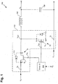
- FIG. 1 shows an exemplary circuit schematic of synchronous buck converter 100 including half-bridge 102, which is formed in a stacked half-bridge package according to an embodiment of the invention, and is thus also referred to as "stacked half-bridge package” 102 or “half-bridge package” 102 in the present application.
- Synchronous buck converter 100 also includes, driver integrated circuit (IC) 104, output inductor 106, and output capacitor 108.
- IC driver integrated circuit
- Half-bridge package 102 includes control transistor Q 1 and synchronous transistor Q 2 (also referred to as “sync transistor"), high voltage input terminal V H , low voltage input terminal V L , output terminal V out , control gate terminal V G1 , and sync gate terminal V G2 .
- high voltage input terminal V H receives high voltage input V HI , which can be, for example, a direct current (DC) voltage.
- Low voltage input terminal V L receives low voltage input V LI , which can be, for example, ground.
- control gate terminal V G1 receives a control gate signal from driver IC 104 for driving control transistor Q 1 .
- sync gate terminal V G2 receives a sync gate signal from driver IC 104 for driving sync transistor Q 2 .
- Driver IC 104 may drive control transistor Q 1 and sync transistor Q 2 utilizing any suitable method.
- driver IC 104 can vary a duty cycle of the sync and control gate signals responsive to a measurement of output voltage V O of synchronous buck converter 100 to maintain a desired output voltage V O , regardless of changes in high voltage input V HI . It will be appreciated that in other embodiments, output voltage V O is not measured in synchronous buck converter 100.
- Control transistor Q 1 includes control source S 1 , control drain D 1 , and control gate G 1 .
- Sync transistor Q 2 includes sync source S 2 , sync drain D 2 , and sync gate G 2 .
- control transistor Q 1 and sync transistor Q 2 can be any combination of an enhancement more transistor and a depletion mode transistor.
- control transistor Q 1 and sync transistor Q 2 are both depletion mode transistors.
- Control transistor Q 1 and sync transistor Q 2 can be P-channel or N-channel transistors.
- control transistor Q 1 and sync transistor Q 2 can be field-effect transistors (FETs).
- at least one of control transistor Q 1 and sync transistor Q 2 is a silicon FET.
- control transistor Q 1 and sync transistor Q 2 may also comprise a non-silicon FET or any other FET in general.
- at least one of control transistor Q 1 and sync transistor Q 2 is a metal-oxide-semiconductor field-effect transistor (MOSFET).
- MOSFET metal-oxide-semiconductor field-effect transistor
- At least one of control transistor Q 1 and sync transistor Q 2 can also be, as an example, a high electron mobility transistor (HEMT), such as a GaN HEMT.
- HEMT high electron mobility transistor
- Control transistor Q 1 has control drain D 1 for connection to high voltage input V H1 through high voltage input terminal V H of half-bridge package 102. Control transistor Q 1 also has control source S 1 coupled to output terminal V OUT of half-bridge package 102. Also, control transistor Q 1 has control gate G 1 coupled to control gate terminal V G1 of half-bridge package 102 for being driven by driver IC 104.
- Sync transistor Q 2 has sync drain D 2 for connection to output terminal V OUT of half-bridge package 102.
- Sync transistor Q 2 also has sync source S 2 coupled to low voltage input V LI through low voltage input terminal V L of half-bridge package 102.
- sync transistor Q 2 has sync gate G 2 coupled to sync gate terminal V G2 of half-bridge package 102 for being driven by driver IC 104.
- control transistor Q 1 and sync transistor Q 2 can be connected to a diode.
- Figure 1 shows optional diodes 110 and 112.
- diode 110 is coupled to control source Si and control drain D 1 , such that diode 110 is in parallel with control transistor Q 1 .
- diode 112 is coupled to sync source S 2 and sync drain D 2 , such that diode 112 is in parallel with control transistor Q 2 .
- at least one of diodes 110 and 112 can be connected with a reverse polarity to that shown in Figure 1 .
- diodes 110 and 112 can be internal to or external to control transistor Q 1 and sync transistor Q 2 .
- control transistor Q 1 and sync transistor Q 2 are MOSFETs and diodes 110 and 112 are respective body diodes of control transistor Q 1 and sync transistor Q 2 .
- Control transistor Q 1 and sync transistor Q 2 are commonly included on respective dies (i.e. a control transistor die and a synchronous transistor die).
- the respective dies may include other components, for example, diode 110 may be on the control transistor die and diode 112 may be on the synchronous transistor die. These other components may also be provided external to the respective dies and can be, for example, on a different die.
- Synchronous buck converter 100 illustrates one power converter, which can benefit from including stacked half-bridge package 102, in accordance with embodiments of the present invention.
- half-bridge package 102 is not limited to being included in a synchronous buck converter and can be included in other types of power converters.
- control transistor Q 1 and sync transistor Q 2 can be connected in a stacked half-bridge package, which includes stacked half-bridge package 102, while achieving a small footprint with low parasitic inductance and resistance.
- the stacked half-bridge package can have a small form factor where the stacked half-bridge package does not significantly degrade performance of half-bridge 102.
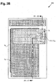
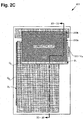
- Figures 2A-2C illustrate selective top views of stacked half-bridge package 202, corresponding to stacked half-bridge package 102 in Figure 1 , in accordance with one embodiment of the present invention.
- Various features of stacked half-bridge package 202 are not shown in Figures 2A-2C for clarity of description.
- Figure 2D illustrates a cross sectional view of a portion of stacked half-bridge package 202, according to one embodiment of the invention. The cross sectional view shown in Figure 2D corresponds to a cross section along line 2D-2D in Figures 2A-2C .
- FIG 2A shows control drain leadframe 220, control gate leadframe 222, common conductive leadframe 224, and sync transistor Q 2 of stacked half-bridge package 202.
- Sync transistor Q 2 in Figures 2A-2D corresponds to sync transistor Q 2 in Figure 1 .
- Common conductive lead frame 224 is over sync transistor Q 2 .
- dashed lines indicate portions of synch transistor Q 2 that would not otherwise be visible, as they are covered by common conductive leadframe 224.
- an outline of synch transistor Q 2 which can be a semiconductor die, is depicted using a dashed line.
- sync transistor Q 2 includes sync source S 2 and sync gate G 2 , which are depicted using dashed lines.
- Sync transistor Q 2 also includes sync drain D 2 , a portion of which is shown in Figure 2A , as it is not fully covered by common conductive leadframe 224 in the present embodiment.
- Sync source S 2 in stacked half-bridge package 202 corresponds to sync source S 2 in Figure 1
- sync gate G 2 in stacked half-bridge package 202 corresponds to sync gate G 2 in Figure 1
- sync drain D 2 in stacked half-bridge package 202 corresponds to sync drain D 2 in Figure 1
- sync transistor Q 2 has top and bottom surfaces, which are opposite one another. Sync drain D 2 is on the top surface and sync source S 2 and sync gate G 2 are on the bottom surface.
- sync drain D 2 is provided with a sync drain pad that substantially covers an entirety of the top surface of sync transistor Q 2 .
- sync source S 2 is provided with a plurality of sync source pads 228a, 228b, 228c, 228d, and 228e (also referred to collectively as "sync source pads 228").
- Sync source S 2 is exposed for electrical connection on a bottom surface of sync transistor Q 2 via sync source pads 228 (See Figure 2D ) and corresponds to low voltage input terminal V L in Figure 1 .
- Sync source pads 228 of sync source S 2 can include solderable front metal (SFM) that can be used for electrical connection to sync source S 2 .
- SFM solderable front metal
- sync gate G 2 is also exposed for electrical connection on a bottom surface of sync transistor Q 2 via a gate pad (See Figure 2D ) and corresponds to sync gate terminal V G2 in Figure 1 .
- Sync gate G 2 can also include SFM that can be used for electrical connection to sync source G 2 .
- sync drain D 2 , sync source S 2 , and sync gate G 2 are not provided as shown in stacked half-bridge package 202.
- sync drain D 2 , sync source S 2 , and sync gate G 2 can be provided on different surfaces of sync transistor Q 2 and can be provided using one or more pads arranged in any suitable manner.
- a single sync source pad can replace sync source pads 228.
- sync source S 2 and sync gate G 2 are not exposed for electrical connection as described above, and other layers or features can be connected to sync source S 2 and sync gate G 2 .
- Control drain leadframe 220, control gate leadframe 222, and common conductive leadframe 224 are electrically conductive and can comprise, for example, an easily solderable metal such as aluminum, and other solderable materials such as a metal alloy or a tri-metal.
- Common conductive leadframe 224 is over sync transistor Q 2 and is electrically and mechanically connected to sync drain D 2 .
- Figure 2B is similar to Figure 2A , with an addition of showing control transistor Q 1 of stacked half-bridge package 202 over common conductive leadframe 224 and sync transistor Q 2 .
- Control transistor Q 1 in stacked half-bridge package 202 corresponds to control transistor Q 1 in Figure 1 .
- dashed lines indicate portions of control transistor Q 1 that would not otherwise be visible. More particularly, control transistor Q 1 includes control source S 1 and control gate G 1 , which are depicted using dashed lines. Control transistor Q 1 also includes control drain D 1 , which is visible in Figure 2B .
- Control source S 1 in stacked half-bridge package 202 corresponds to control source S 1 in Figure 1
- control gate G 1 in stacked half-bridge package 202 corresponds to control gate G 1 in Figure 1
- control drain D 1 in stacked half-bridge package 202 corresponds to control drain D 1 in Figure 1
- control transistor Q 1 has top and bottom surfaces, which are opposite one another. Control drain D 1 is on the top surface and control source S 1 and control gate G 1 are on the bottom surface.
- control drain D 1 is provided with a control drain pad that substantially covers an entirety of the top surface of control transistor Q 1 .
- control source S 1 is provided with a plurality of control source pads 234a and 234b (also referred to as control source pads 234). In some embodiments, a single control source pad can replace control source pads 234.
- Control transistor Q 1 is over common conductive leadframe 224, which is electrically and mechanically connected to control source S 1 .
- control and sync transistors Q 1 and Q 2 are stacked on opposite sides of common conductive leadframe 224, with common conductive leadframe 224 electrically and mechanically coupling control source S 1 with sync drain D 2 .
- Common conductive leadframe 224 is thereby serving as output terminal V OUT of stacked half-bridge package 202, corresponding to output terminal V OUT in Figure 1 .
- a short current path is formed between control source S 1 and sync drain D 2 that has low parasitic inductance and resistance (See Figure 2D ).
- stacked half-bridge package 202 does not significantly degrade performance of half-bridge 102 in Figure 1 .
- stacked half-bridge package 202 has a small footprint that does not incorporate footprints of control transistor Q 1 and sync transistor Q 2 individually, thereby allowing for a small form factor.
- Control transistor Q 1 is also over control gate leadframe 222, which is electrically and mechanically connected to control gate G 2 .
- control gate leadframe 222 corresponds to control gate terminal V G1 in Figure 1 .
- Control gate leadframe 222 provides electrical and mechanical connection for control gate G 1 .
- Figure 2B shows a majority of control transistor Q 1 being over common conductive leadframe 224, with a portion of control transistor Q 1 overhanging common conductive leadframe 224 so as to accommodate connection between control gate G 1 and control gate leadframe 222.
- Figure 2C is similar to Figure 2B , with an addition of showing conductive clip 230 of stacked half-bridge package 202 over control transistor Q 1 , common conductive leadframe 224 and sync transistor Q 2 .
- Conductive clip 230 comprises conductive material, such as a metal or metal alloy. In one embodiment conductive clip 230 is a copper clip.
- Conductive clip 230 includes web portion 230a and leg portion 230b and provides connection between control drain D 1 and control drain leadframe 220.
- a dashed line indicates a boundary of web portion 230a and leg portion 230b.
- control drain leadframe 220 corresponds to high voltage input terminal V H in Figure 1 with leg portion 230b being over and electrically and mechanically connected to control drain leadframe 220 and web portion 230a being over and electrically and mechanically connected to control drain D 1 of control transistor Q 1 .
- Figure 2D illustrates a cross sectional view of a portion of stacked half-bridge package 202 corresponding to a cross section along line 2D-2D in Figures 2A-2C .
- Figure 2D shows hermetic sealant 236, which is optional as indicated by dashed lines.
- hermetic sealant 236 is a molding compound, which encapsulates stacked half-bridge package 202.
- Figure 2D shows hermetic sealant 236 leaves common conductive leadframe 224, sync gate G 2 , sync source S 2 , control gate leadframe 222, and control drain leadframe 220 exposed on bottomside 240b of stacked half-bridge package 202 and thus, available for electrical connection.
- FIG. 2D shows that in the present embodiment, common conductive leadframe 224 has web portion 224a and leg portion 224b.
- Leg portion 224b is of thickness 242, which is greater than that of sync transistor Q 2 and web portion 224a.
- control gate leadframe 222 is of thickness 242, which is greater than that of web portion 224a of common conductive leadframe 224 and is greater than that of sync transistor Q 1 .
- control drain leadframe 220 is of thickness 244, which is greater than that of web portion 224a of common conductive leadframe 224 and is greater than that of sync transistor Q 1 .
- respective bottom surfaces of sync transistor Q 1 , leg portion 224a of common conductive leadframe 224, conductive gate leadframe 222 and conductive drain leadframe 220 can thereby be substantially flush with one another, as shown in Figure 2D .
- stacked half-bridge package 202 can easily be mounted on and electrically connected to a substrate (not shown in Figures 2A-2D ).
- Figure 2D also shows that conductive clip 230 is connected to control drain D 2 at topside 240a of stacked half-bridge package 202.
- Leg portion 230b of conductive clip 230 is of thickness 244 that is greater than that of control transistor Q 1 and web portion 230a.
- respective top surfaces of control gate leadframe 222, control drain leadframe 220, and common conductive leadframe 224 can thereby be substantially flush with one another, as shown in Figure 2D .
- control gate leadframe 222, control drain leadframe 220, and common conductive leadframe 224 can be formed from a shared leadframe.
- common conductive leadframe 224 is an etched or half-etched leadframe that can be formed from the shared leadframe.
- Etching or half-etching common conductive leadframe 224 can be used to form leg portion 224b of common conductive leadframe 224.
- Figure 2D also illustrates that common conductive leadframe 224 electrically and mechanically couples the control source (source of control transistor Q1) with the sync drain (drain of sync transistor Q2) to form the output terminal of stacked half-bridge package 202.
- embodiments of the present invention can provide for a stacked half-bridge package including a control transistor and a sync transistor.
- the control transistor and the sync transistor can advantageously be connected in a half-bridge package with low parasitic inductance and resistance.
- the control transistor and the sync transistor can be connected with the stacked half-bridge package having a small footprint.
- the stacked half-bridge package can have a small form factor, where the stacked half-bridge package does not significantly degrade performance of the half-bridge.
Description
- The present invention relates generally to semiconductor devices. More particularly, the present invention relates to packaging of semiconductor devices.
- To allow for high efficiency power conversion, power converters, such as buck converters, commonly employ power switching circuits in which a high side power transistor and a low side power transistor are connected to form a half-bridge. One such power converter that is frequently employed is a synchronous buck converter, where the high side transistor is a control transistor and the low side transistor is a synchronous transistor. The control transistor and the synchronous transistor are typically formed on their respective separate dies, i.e. a control transistor die and a synchronous transistor die, that are connected in a package (i.e. co-packaged) to form the half-bridge.
- One approach to connecting the control transistor and the synchronous transistor in a package would be to arrange the control transistor and the synchronous transistor side by side on a substrate, such as a printed circuit board (PCB). However, this arrangement would result in the package having a large footprint, as the package must be large enough to accommodate footprints of the control transistor and the synchronous transistor. Furthermore, conductive traces on the PCB could be used to connect the control transistor and the synchronous transistor so as to form the half-bridge package. However, the conductive traces would form long routing paths on the PCB, causing high parasitic inductance and resistance. Thus, this approach to packaging the control transistor and the synchronous transistor would result in a package having a large form factor where the package significantly degrades performance of the half-bridge.
- What is needed is an approach to packaging control and synchronous transistors that is capable of achieving packages having a small form factor where the packages do not significantly degrade performance of the half-bridge.
-
US 2006/169976 A1 discloses a stacked half bridge packet in accordance with the preamble ofclaim 1. The said document, however, is quiet regarding the relationship between the control source and the control gate on the one side and the control drain on the other side of the control transistor. -
US 2008/061396 A1 neither comprises the limitations of the preamble ofclaim 1, nor those of the characterizing part. - A stacked half-bridge package with a common conductive leadframe, substantially as shown in and/or described in connection with at least one of the figures, and as set forth more completely in the claims.
-
-
Figure 1 shows an exemplary circuit schematic of a synchronous buck converter, according to one embodiment of the invention. -
Figure 2A illustrates a selective top view of a stacked half-bridge package, according to one embodiment of the invention. -
Figure 2B illustrates a selective top view of a stacked half-bridge package, according to one embodiment of the invention. -
Figure 2C illustrates a selective top view of a stacked half-bridge package, according to one embodiment of the invention. -
Figure 2D illustrates a cross sectional view of a portion of a stacked half-bridge package, according to one embodiment of the invention. - The present application is directed to a stacked half-bridge package with a common conductive leadframe. The following description contains specific information pertaining to the implementation of the present invention. One skilled in the art will recognize that the present invention may be implemented in a manner different from that specifically discussed in the present application. Moreover, some of the specific details of the invention are not discussed in order not to obscure the invention. The specific details not described in the present application are within the knowledge of a person of ordinary skill in the art.
- The drawings in the present application and their accompanying detailed description are directed to merely exemplary embodiments of the invention. To maintain brevity, other embodiments of the invention, which use the principles of the present invention, are not specifically described in the present application and are not specifically illustrated by the present drawings.
-
Figure 1 shows an exemplary circuit schematic ofsynchronous buck converter 100 including half-bridge 102, which is formed in a stacked half-bridge package according to an embodiment of the invention, and is thus also referred to as "stacked half-bridge package" 102 or "half-bridge package" 102 in the present application.Synchronous buck converter 100 also includes, driver integrated circuit (IC) 104,output inductor 106, andoutput capacitor 108. - Half-
bridge package 102 includes control transistor Q1 and synchronous transistor Q2 (also referred to as "sync transistor"), high voltage input terminal VH, low voltage input terminal VL, output terminal Vout, control gate terminal VG1, and sync gate terminal VG2. - In half-
bridge package 102, high voltage input terminal VH receives high voltage input VHI, which can be, for example, a direct current (DC) voltage. Low voltage input terminal VL receives low voltage input VLI, which can be, for example, ground. Also in half-bridge package 102, control gate terminal VG1 receives a control gate signal fromdriver IC 104 for driving control transistor Q1. Similarly, sync gate terminal VG2 receives a sync gate signal fromdriver IC 104 for driving sync transistor Q2. Driver IC 104 may drive control transistor Q1 and sync transistor Q2 utilizing any suitable method. As a specific example, in one embodiment,driver IC 104 can vary a duty cycle of the sync and control gate signals responsive to a measurement of output voltage VO ofsynchronous buck converter 100 to maintain a desired output voltage VO, regardless of changes in high voltage input VHI. It will be appreciated that in other embodiments, output voltage VO is not measured insynchronous buck converter 100. - Control transistor Q1 includes control source S1, control drain D1, and control gate G1. Sync transistor Q2 includes sync source S2, sync drain D2, and sync gate G2. In various embodiments of the present invention, control transistor Q1 and sync transistor Q2 can be any combination of an enhancement more transistor and a depletion mode transistor. For example, in one embodiment, control transistor Q1 and sync transistor Q2 are both depletion mode transistors. Control transistor Q1 and sync transistor Q2 can be P-channel or N-channel transistors. Also, control transistor Q1 and sync transistor Q2 can be field-effect transistors (FETs). In one embodiment, at least one of control transistor Q1 and sync transistor Q2 is a silicon FET. However, at least one of control transistor Q1 and sync transistor Q2 may also comprise a non-silicon FET or any other FET in general. In one embodiment, at least one of control transistor Q1 and sync transistor Q2 is a metal-oxide-semiconductor field-effect transistor (MOSFET). At least one of control transistor Q1 and sync transistor Q2 can also be, as an example, a high electron mobility transistor (HEMT), such as a GaN HEMT.
- Control transistor Q1 has control drain D1 for connection to high voltage input VH1 through high voltage input terminal VH of half-
bridge package 102. Control transistor Q1 also has control source S1 coupled to output terminal VOUT of half-bridge package 102. Also, control transistor Q1 has control gate G1 coupled to control gate terminal VG1 of half-bridge package 102 for being driven by driver IC 104. - Sync transistor Q2 has sync drain D2 for connection to output terminal VOUT of half-
bridge package 102. Sync transistor Q2 also has sync source S2 coupled to low voltage input VLI through low voltage input terminal VL of half-bridge package 102. Also, sync transistor Q2 has sync gate G2 coupled to sync gate terminal VG2 of half-bridge package 102 for being driven by driver IC 104. - In some embodiments, at least one of control transistor Q1 and sync transistor Q2 can be connected to a diode. For example,
Figure 1 showsoptional diodes Figure 1 ,diode 110 is coupled to control source Si and control drain D1, such thatdiode 110 is in parallel with control transistor Q1. Similarly,diode 112 is coupled to sync source S2 and sync drain D2, such thatdiode 112 is in parallel with control transistor Q2. In some embodiments, at least one ofdiodes Figure 1 . In various embodiments,diodes diodes - Control transistor Q1 and sync transistor Q2 are commonly included on respective dies (i.e. a control transistor die and a synchronous transistor die). The respective dies may include other components, for example,
diode 110 may be on the control transistor die anddiode 112 may be on the synchronous transistor die. These other components may also be provided external to the respective dies and can be, for example, on a different die. -
Synchronous buck converter 100 illustrates one power converter, which can benefit from including stacked half-bridge package 102, in accordance with embodiments of the present invention. However, half-bridge package 102 is not limited to being included in a synchronous buck converter and can be included in other types of power converters. - In accordance with embodiments of the present invention, control transistor Q1 and sync transistor Q2 can be connected in a stacked half-bridge package, which includes stacked half-
bridge package 102, while achieving a small footprint with low parasitic inductance and resistance. Thus, the stacked half-bridge package can have a small form factor where the stacked half-bridge package does not significantly degrade performance of half-bridge 102. -
Figures 2A-2C illustrate selective top views of stacked half-bridge package 202, corresponding to stacked half-bridge package 102 inFigure 1 , in accordance with one embodiment of the present invention. Various features of stacked half-bridge package 202 are not shown inFigures 2A-2C for clarity of description.Figure 2D illustrates a cross sectional view of a portion of stacked half-bridge package 202, according to one embodiment of the invention. The cross sectional view shown inFigure 2D corresponds to a cross section alongline 2D-2D inFigures 2A-2C . -
Figure 2A showscontrol drain leadframe 220,control gate leadframe 222, commonconductive leadframe 224, and sync transistor Q2 of stacked half-bridge package 202. Sync transistor Q2 inFigures 2A-2D corresponds to sync transistor Q2 inFigure 1 . Common conductivelead frame 224 is over sync transistor Q2. InFigure 2A , dashed lines indicate portions of synch transistor Q2 that would not otherwise be visible, as they are covered by commonconductive leadframe 224. For example, an outline of synch transistor Q2, which can be a semiconductor die, is depicted using a dashed line. Furthermore, sync transistor Q2 includes sync source S2 and sync gate G2, which are depicted using dashed lines. Sync transistor Q2 also includes sync drain D2, a portion of which is shown inFigure 2A , as it is not fully covered by commonconductive leadframe 224 in the present embodiment. - Sync source S2 in stacked half-
bridge package 202 corresponds to sync source S2 inFigure 1 , sync gate G2 in stacked half-bridge package 202 corresponds to sync gate G2 inFigure 1 , and sync drain D2 in stacked half-bridge package 202 corresponds to sync drain D2 inFigure 1 . In the present embodiment, sync transistor Q2 has top and bottom surfaces, which are opposite one another. Sync drain D2 is on the top surface and sync source S2 and sync gate G2 are on the bottom surface. - Also in the present embodiment, sync drain D2 is provided with a sync drain pad that substantially covers an entirety of the top surface of sync transistor Q2. Furthermore, sync source S2 is provided with a plurality of
sync source pads Figure 2D ) and corresponds to low voltage input terminal VL inFigure 1 . Sync source pads 228 of sync source S2 can include solderable front metal (SFM) that can be used for electrical connection to sync source S2. - In the present embodiment, sync gate G2 is also exposed for electrical connection on a bottom surface of sync transistor Q2 via a gate pad (See
Figure 2D ) and corresponds to sync gate terminal VG2 inFigure 1 . Sync gate G2 can also include SFM that can be used for electrical connection to sync source G2. - It is noted that in some embodiments, sync drain D2, sync source S2, and sync gate G2 are not provided as shown in stacked half-
bridge package 202. For example, sync drain D2, sync source S2, and sync gate G2 can be provided on different surfaces of sync transistor Q2 and can be provided using one or more pads arranged in any suitable manner. As one example, in some embodiments, a single sync source pad can replace sync source pads 228. It is further noted that in some embodiments, sync source S2 and sync gate G2 are not exposed for electrical connection as described above, and other layers or features can be connected to sync source S2 and sync gate G2. -
Control drain leadframe 220,control gate leadframe 222, and commonconductive leadframe 224 are electrically conductive and can comprise, for example, an easily solderable metal such as aluminum, and other solderable materials such as a metal alloy or a tri-metal. Commonconductive leadframe 224 is over sync transistor Q2 and is electrically and mechanically connected to sync drain D2. -
Figure 2B is similar toFigure 2A , with an addition of showing control transistor Q1 of stacked half-bridge package 202 over commonconductive leadframe 224 and sync transistor Q2. Control transistor Q1 in stacked half-bridge package 202 corresponds to control transistor Q1 inFigure 1 . InFigure 2B , dashed lines indicate portions of control transistor Q1 that would not otherwise be visible. More particularly, control transistor Q1 includes control source S1 and control gate G1, which are depicted using dashed lines. Control transistor Q1 also includes control drain D1, which is visible inFigure 2B . - Control source S1 in stacked half-
bridge package 202 corresponds to control source S1 inFigure 1 , control gate G1 in stacked half-bridge package 202 corresponds to control gate G1 inFigure 1 , and control drain D1 in stacked half-bridge package 202 corresponds to control drain D1 inFigure 1 . In the present embodiment, control transistor Q1 has top and bottom surfaces, which are opposite one another. Control drain D1 is on the top surface and control source S1 and control gate G1 are on the bottom surface. - In the present embodiment, control drain D1 is provided with a control drain pad that substantially covers an entirety of the top surface of control transistor Q1. Also in the present embodiment, control source S1 is provided with a plurality of
control source pads - Control transistor Q1 is over common
conductive leadframe 224, which is electrically and mechanically connected to control source S1. Thus, control and sync transistors Q1 and Q2 are stacked on opposite sides of commonconductive leadframe 224, with commonconductive leadframe 224 electrically and mechanically coupling control source S1 with sync drain D2. Commonconductive leadframe 224 is thereby serving as output terminal VOUT of stacked half-bridge package 202, corresponding to output terminal VOUT inFigure 1 . Advantageously, a short current path is formed between control source S1 and sync drain D2 that has low parasitic inductance and resistance (SeeFigure 2D ). As such, stacked half-bridge package 202 does not significantly degrade performance of half-bridge 102 inFigure 1 . Furthermore, stacked half-bridge package 202 has a small footprint that does not incorporate footprints of control transistor Q1 and sync transistor Q2 individually, thereby allowing for a small form factor. - Control transistor Q1 is also over
control gate leadframe 222, which is electrically and mechanically connected to control gate G2. In the present embodiment,control gate leadframe 222 corresponds to control gate terminal VG1 inFigure 1 .Control gate leadframe 222 provides electrical and mechanical connection for control gate G1.Figure 2B shows a majority of control transistor Q1 being over commonconductive leadframe 224, with a portion of control transistor Q1 overhanging commonconductive leadframe 224 so as to accommodate connection between control gate G1 and controlgate leadframe 222. -
Figure 2C is similar toFigure 2B , with an addition of showingconductive clip 230 of stacked half-bridge package 202 over control transistor Q1, commonconductive leadframe 224 and sync transistor Q2.Conductive clip 230 comprises conductive material, such as a metal or metal alloy. In one embodimentconductive clip 230 is a copper clip.Conductive clip 230 includesweb portion 230a andleg portion 230b and provides connection between control drain D1 andcontrol drain leadframe 220. InFigure 2C , a dashed line indicates a boundary ofweb portion 230a andleg portion 230b. In the present embodiment,control drain leadframe 220 corresponds to high voltage input terminal VH inFigure 1 withleg portion 230b being over and electrically and mechanically connected to controldrain leadframe 220 andweb portion 230a being over and electrically and mechanically connected to control drain D1 of control transistor Q1. - As noted above,
Figure 2D illustrates a cross sectional view of a portion of stacked half-bridge package 202 corresponding to a cross section alongline 2D-2D inFigures 2A-2C .Figure 2D showshermetic sealant 236, which is optional as indicated by dashed lines. In one embodiment,hermetic sealant 236 is a molding compound, which encapsulates stacked half-bridge package 202.Figure 2D showshermetic sealant 236 leaves commonconductive leadframe 224, sync gate G2, sync source S2,control gate leadframe 222, andcontrol drain leadframe 220 exposed onbottomside 240b of stacked half-bridge package 202 and thus, available for electrical connection. -
Figure 2D shows that in the present embodiment, commonconductive leadframe 224 hasweb portion 224a and leg portion 224b. Leg portion 224b is ofthickness 242, which is greater than that of sync transistor Q2 andweb portion 224a. Furthermore,control gate leadframe 222 is ofthickness 242, which is greater than that ofweb portion 224a of commonconductive leadframe 224 and is greater than that of sync transistor Q1. Similarly,control drain leadframe 220 is ofthickness 244, which is greater than that ofweb portion 224a of commonconductive leadframe 224 and is greater than that of sync transistor Q1. In the present embodiment, respective bottom surfaces of sync transistor Q1,leg portion 224a of commonconductive leadframe 224,conductive gate leadframe 222 andconductive drain leadframe 220 can thereby be substantially flush with one another, as shown inFigure 2D . As such, stacked half-bridge package 202 can easily be mounted on and electrically connected to a substrate (not shown inFigures 2A-2D ). -
Figure 2D also shows thatconductive clip 230 is connected to control drain D2 at topside 240a of stacked half-bridge package 202.Leg portion 230b ofconductive clip 230 is ofthickness 244 that is greater than that of control transistor Q1 andweb portion 230a. In the present embodiment, respective top surfaces ofcontrol gate leadframe 222,control drain leadframe 220, and commonconductive leadframe 224 can thereby be substantially flush with one another, as shown inFigure 2D . Thus, in some embodiments,control gate leadframe 222,control drain leadframe 220, and commonconductive leadframe 224 can be formed from a shared leadframe. In one embodiment, commonconductive leadframe 224 is an etched or half-etched leadframe that can be formed from the shared leadframe. Etching or half-etching commonconductive leadframe 224 can be used to form leg portion 224b of commonconductive leadframe 224.Figure 2D also illustrates that commonconductive leadframe 224 electrically and mechanically couples the control source (source of control transistor Q1) with the sync drain (drain of sync transistor Q2) to form the output terminal of stacked half-bridge package 202. - Thus, as described above with respect to
Figures 1 and2A-2D , embodiments of the present invention can provide for a stacked half-bridge package including a control transistor and a sync transistor. The control transistor and the sync transistor can advantageously be connected in a half-bridge package with low parasitic inductance and resistance. Furthermore, the control transistor and the sync transistor can be connected with the stacked half-bridge package having a small footprint. As such, among other advantages not specifically described herein, the stacked half-bridge package can have a small form factor, where the stacked half-bridge package does not significantly degrade performance of the half-bridge.
Claims (14)
- A stacked half-bridge package (202) comprising:a control transistor (Q1) having a control drain (D1) for connection to a high voltage input (VH), a control source (S1) coupled to an output terminal (VOUT), and a control gate (G1) for being driven by a driver IC;a sync transistor (Q2) having a sync drain (D2) for connection to said output terminal (VOUT), a sync source (S2) coupled to a low voltage input (VLI), and a sync gate (G2) for being driven by said driver IC;said control (Q1) and sync (Q2) transistors being stacked on opposite sides of a common conductive leadframe (224), said common conductive leadframe (224) electrically and mechanically coupling said control source (S1) with said sync drain (D2), said common conductive leadframe (224) thereby serving as said output terminal (VOUT) characterized in that said control source (S1) and said control gate (G1) being on a surface of said control transistor (Q1) opposite of said control drain (D1),wherein a control gate leadframe (222) provides mechanical and electrical connection for said control gate (G1).
- The stacked half-bridge package (202) of claim 1, wherein said common conductive leadframe (224) comprises a web portion (224a) and a leg portion (224b).
- The stacked half-bridge package (202) of claim 1, wherein said common conductive leadframe (224) comprises a leg portion (224b) that is of a thickness greater than said sync transistor (Q2).
- The stacked half-bridge package (202) of claim 1, wherein respective bottom surfaces of said sync transistor (Q2) and a leg portion (224b) of said common conductive leadframe (224) are flush with one another.
- The stacked half-bridge package (202) of claim 1, wherein a conductive clip (230) provides connection between said control drain (D1) and a control drain leadframe (220).
- The stacked half-bridge package (202) of claim 1, comprising a conductive clip (230) including a web portion (230a) that is electrically and mechanically connected to said control drain (D1) and including a leg portion (230b) that is electrically and mechanically connected to a control drain leadframe (220).
- The stacked half-bridge package (202) of claim 1, wherein a conductive clip (230) is connected to said control drain (D1) at a topside (240a) of said stacked half-bridge package (202).
- The stacked half-bridge package (202) of claim 1, wherein said common conductive leadframe (224) is a half-etched leadframe.
- The stacked half-bridge package (202) of claim 1, wherein said sync source (S2) comprises a plurality of sync source pads (228a-228e).
- The stacked half-bridge package (202) of claim 1, wherein said sync source (S2) comprises a solderable front metal (SFM) (228).
- The stacked half-bridge package (202) of claim 1, wherein said sync source (S2) is exposed for electrical connection on a bottom surface of said sync transistor (Q2).
- The stacked half-bridge package (202) of claim 1, wherein said sync gate (G2) is exposed for electrical connection on a bottom surface of said sync transistor (Q2).
- The stacked half-bridge package (202) of claim 1, wherein said control transistor (Q1) has top and bottom surfaces, said control drain (D1) being on said top surface and said control source (S1) and said control gate (G1) being on said bottom surface.
- The stacked half-bridge package (202) of claim 1, wherein said sync transistor (Q2) has top and bottom surfaces, said sync drain (D2) being on said top surface and said sync source (S2) and said sync gate (G2) being on said bottom surface.
Applications Claiming Priority (2)
| Application Number | Priority Date | Filing Date | Title |
|---|---|---|---|
| US201161461110P | 2011-01-14 | 2011-01-14 | |
| US13/278,695 US8426952B2 (en) | 2011-01-14 | 2011-10-21 | Stacked half-bridge package with a common conductive leadframe |
Publications (3)
| Publication Number | Publication Date |
|---|---|
| EP2477221A2 EP2477221A2 (en) | 2012-07-18 |
| EP2477221A3 EP2477221A3 (en) | 2014-09-17 |
| EP2477221B1 true EP2477221B1 (en) | 2016-06-22 |
Family
ID=45047676
Family Applications (1)
| Application Number | Title | Priority Date | Filing Date |
|---|---|---|---|
| EP11191634.2A Active EP2477221B1 (en) | 2011-01-14 | 2011-12-01 | Stacked half-bridge package with a common conductive leadframe |
Country Status (2)
| Country | Link |
|---|---|
| US (3) | US8426952B2 (en) |
| EP (1) | EP2477221B1 (en) |
Families Citing this family (34)
| Publication number | Priority date | Publication date | Assignee | Title |
|---|---|---|---|---|
| US9236378B2 (en) | 2010-08-11 | 2016-01-12 | Sarda Technologies, Inc. | Integrated switch devices |
| US8637909B1 (en) * | 2010-08-11 | 2014-01-28 | Sarda Technologies, Inc. | Mixed mode dual switch |
| US8896034B1 (en) | 2010-08-11 | 2014-11-25 | Sarda Technologies, Inc. | Radio frequency and microwave devices and methods of use |
| TWI453831B (en) | 2010-09-09 | 2014-09-21 | 台灣捷康綜合有限公司 | Semiconductor package and method for making the same |
| US8896107B2 (en) * | 2011-01-03 | 2014-11-25 | International Rectifier Corporation | High power semiconductor package with conductive clip |
| US8680627B2 (en) * | 2011-01-14 | 2014-03-25 | International Rectifier Corporation | Stacked half-bridge package with a common conductive clip |
| US8426952B2 (en) * | 2011-01-14 | 2013-04-23 | International Rectifier Corporation | Stacked half-bridge package with a common conductive leadframe |
| US8674497B2 (en) | 2011-01-14 | 2014-03-18 | International Business Machines Corporation | Stacked half-bridge package with a current carrying layer |
| US8648643B2 (en) | 2012-02-24 | 2014-02-11 | Transphorm Inc. | Semiconductor power modules and devices |
| US9111921B2 (en) * | 2012-10-18 | 2015-08-18 | International Rectifier Corporation | Semiconductor package with conductive carrier integrated heat spreader |
| US9111776B2 (en) | 2012-10-18 | 2015-08-18 | International Rectifier Corporation | Power semiconductor package with non-contiguous, multi-section conductive carrier |
| US8860194B2 (en) * | 2012-11-01 | 2014-10-14 | International Rectifier Corporation | Buck converter power package |
| US9171837B2 (en) * | 2012-12-17 | 2015-10-27 | Nxp B.V. | Cascode circuit |
| US9379050B2 (en) * | 2013-02-28 | 2016-06-28 | Infineon Technologies Austria Ag | Electronic device |
| US9589929B2 (en) | 2013-03-14 | 2017-03-07 | Vishay-Siliconix | Method for fabricating stack die package |
| WO2014159471A1 (en) | 2013-03-14 | 2014-10-02 | Vishay-Siliconix | Stack die package |
| US9966330B2 (en) * | 2013-03-14 | 2018-05-08 | Vishay-Siliconix | Stack die package |
| US9385070B2 (en) | 2013-06-28 | 2016-07-05 | Delta Electronics, Inc. | Semiconductor component having a lateral semiconductor device and a vertical semiconductor device |
| US9536800B2 (en) | 2013-12-07 | 2017-01-03 | Fairchild Semiconductor Corporation | Packaged semiconductor devices and methods of manufacturing |
| US9620475B2 (en) | 2013-12-09 | 2017-04-11 | Infineon Technologies Americas Corp | Array based fabrication of power semiconductor package with integrated heat spreader |
| US9704787B2 (en) | 2014-10-16 | 2017-07-11 | Infineon Technologies Americas Corp. | Compact single-die power semiconductor package |
| US9653386B2 (en) * | 2014-10-16 | 2017-05-16 | Infineon Technologies Americas Corp. | Compact multi-die power semiconductor package |
| US9570379B2 (en) | 2013-12-09 | 2017-02-14 | Infineon Technologies Americas Corp. | Power semiconductor package with integrated heat spreader and partially etched conductive carrier |
| US9431327B2 (en) | 2014-05-30 | 2016-08-30 | Delta Electronics, Inc. | Semiconductor device |
| DE102015104990B4 (en) * | 2015-03-31 | 2020-06-04 | Infineon Technologies Austria Ag | Compound semiconductor device with a scanning lead |
| US9774322B1 (en) | 2016-06-22 | 2017-09-26 | Sarda Technologies, Inc. | Gate driver for depletion-mode transistors |
| FR3054929A1 (en) * | 2016-08-05 | 2018-02-09 | Commissariat Energie Atomique | METHOD OF ENCAPSULATING AN INTEGRATED CIRCUIT WITH A HORIZONTAL HETEROJUNCTION TRANSISTOR CHIP |
| US10083897B2 (en) | 2017-02-20 | 2018-09-25 | Silanna Asia Pte Ltd | Connection arrangements for integrated lateral diffusion field effect transistors having a backside contact |
| US9923059B1 (en) | 2017-02-20 | 2018-03-20 | Silanna Asia Pte Ltd | Connection arrangements for integrated lateral diffusion field effect transistors |
| EP3703119B1 (en) * | 2017-10-26 | 2022-06-08 | Shindengen Electric Manufacturing Co., Ltd. | Semiconductor device and method for manufacturing semiconductor device |
| JP7059677B2 (en) * | 2018-02-16 | 2022-04-26 | 富士電機株式会社 | Stacked integrated circuit |
| US11158567B2 (en) * | 2019-08-09 | 2021-10-26 | Texas Instruments Incorporated | Package with stacked power stage and integrated control die |
| CN111463188A (en) * | 2020-05-03 | 2020-07-28 | 矽力杰半导体技术(杭州)有限公司 | Packaging structure applied to power converter |
| US20230178457A1 (en) * | 2021-12-08 | 2023-06-08 | Nxp B.V. | Semiconductor package having lead frame with semiconductor die and component module mounted on opposite surfaces of the lead frame and methods of manufacture thereof |
Family Cites Families (29)
| Publication number | Priority date | Publication date | Assignee | Title |
|---|---|---|---|---|
| JP4426955B2 (en) | 2004-11-30 | 2010-03-03 | 株式会社ルネサステクノロジ | Semiconductor device |
| JP2006216940A (en) * | 2005-01-07 | 2006-08-17 | Toshiba Corp | Semiconductor device |
| JP2006324320A (en) | 2005-05-17 | 2006-11-30 | Renesas Technology Corp | Semiconductor device |
| DE102005055761B4 (en) | 2005-11-21 | 2008-02-07 | Infineon Technologies Ag | Power semiconductor component with semiconductor chip stack in bridge circuit and method for producing the same |
| US7618896B2 (en) | 2006-04-24 | 2009-11-17 | Fairchild Semiconductor Corporation | Semiconductor die package including multiple dies and a common node structure |
| US7859089B2 (en) | 2006-05-04 | 2010-12-28 | International Rectifier Corporation | Copper straps |
| US7485954B2 (en) * | 2006-09-07 | 2009-02-03 | Alpha And Omega Semiconductor Limited | Stacked dual MOSFET package |
| US8674670B2 (en) | 2006-11-28 | 2014-03-18 | International Rectifier Corporation | DC/DC converter with depletion-mode III-nitride switches |
| US7902809B2 (en) | 2006-11-28 | 2011-03-08 | International Rectifier Corporation | DC/DC converter including a depletion mode power switch |
| KR101489325B1 (en) | 2007-03-12 | 2015-02-06 | 페어차일드코리아반도체 주식회사 | Power module with stacked flip-chip and method of fabricating the same power module |
| US7800208B2 (en) | 2007-10-26 | 2010-09-21 | Infineon Technologies Ag | Device with a plurality of semiconductor chips |
| KR101375831B1 (en) | 2007-12-03 | 2014-04-02 | 삼성전자주식회사 | Display device using oxide semiconductor thin film transistor |
| KR20090062612A (en) | 2007-12-13 | 2009-06-17 | 페어차일드코리아반도체 주식회사 | Multi chip package |
| US7781872B2 (en) * | 2007-12-19 | 2010-08-24 | Fairchild Semiconductor Corporation | Package with multiple dies |
| US8642394B2 (en) | 2008-01-28 | 2014-02-04 | Infineon Technologies Ag | Method of manufacturing electronic device on leadframe |
| KR100958006B1 (en) | 2008-06-18 | 2010-05-17 | 삼성모바일디스플레이주식회사 | Thin film transistor, method of manufacturing the thin film transistor and flat panel display device having the thin film transistor |
| US8062932B2 (en) | 2008-12-01 | 2011-11-22 | Alpha & Omega Semiconductor, Inc. | Compact semiconductor package with integrated bypass capacitor and method |
| US20100171543A1 (en) | 2009-01-08 | 2010-07-08 | Ciclon Semiconductor Device Corp. | Packaged power switching device |
| KR101097322B1 (en) | 2009-12-15 | 2011-12-23 | 삼성모바일디스플레이주식회사 | Thin film transistor, method of manufacturing the thin film transistor and organic electroluminiscent device having the thin film transistor |
| US8896107B2 (en) * | 2011-01-03 | 2014-11-25 | International Rectifier Corporation | High power semiconductor package with conductive clip |
| US8426952B2 (en) | 2011-01-14 | 2013-04-23 | International Rectifier Corporation | Stacked half-bridge package with a common conductive leadframe |
| DE102011008952A1 (en) * | 2011-01-19 | 2012-07-19 | Texas Instruments Deutschland Gmbh | Multi-chip module, method of operating the same and DC / DC converter |
| US8431979B2 (en) * | 2011-04-01 | 2013-04-30 | Texas Instruments Incorporated | Power converter having integrated capacitor |
| US8531016B2 (en) * | 2011-05-19 | 2013-09-10 | International Rectifier Corporation | Thermally enhanced semiconductor package with exposed parallel conductive clip |
| US8299588B1 (en) | 2011-07-07 | 2012-10-30 | Texas Instruments Incorporated | Structure and method for uniform current distribution in power supply module |
| US8946880B2 (en) * | 2012-03-23 | 2015-02-03 | Texas Instruments Incorporated | Packaged semiconductor device having multilevel leadframes configured as modules |
| US8860194B2 (en) * | 2012-11-01 | 2014-10-14 | International Rectifier Corporation | Buck converter power package |
| US9214415B2 (en) * | 2013-04-11 | 2015-12-15 | Texas Instruments Incorporated | Integrating multi-output power converters having vertically stacked semiconductor chips |
| US9171828B2 (en) * | 2014-02-05 | 2015-10-27 | Texas Instruments Incorporated | DC-DC converter having terminals of semiconductor chips directly attachable to circuit board |
-
2011
- 2011-10-21 US US13/278,695 patent/US8426952B2/en not_active Expired - Fee Related
- 2011-12-01 EP EP11191634.2A patent/EP2477221B1/en active Active
-
2013
- 2013-04-19 US US13/866,744 patent/US9349677B2/en active Active
-
2016
- 2016-05-17 US US15/157,298 patent/US9583477B2/en active Active
Also Published As
| Publication number | Publication date |
|---|---|
| US20130228794A1 (en) | 2013-09-05 |
| US8426952B2 (en) | 2013-04-23 |
| US9349677B2 (en) | 2016-05-24 |
| EP2477221A2 (en) | 2012-07-18 |
| US20160260697A1 (en) | 2016-09-08 |
| US9583477B2 (en) | 2017-02-28 |
| EP2477221A3 (en) | 2014-09-17 |
| US20120181674A1 (en) | 2012-07-19 |
Similar Documents
| Publication | Publication Date | Title |
|---|---|---|
| EP2477221B1 (en) | Stacked half-bridge package with a common conductive leadframe | |
| EP2477220B1 (en) | Stacked half-bridge package with a common conductive clip | |
| US9601418B2 (en) | Stacked half-bridge package | |
| CN101378053B (en) | High-side and low-side nmosfets composite package | |
| US7615854B2 (en) | Semiconductor package that includes stacked semiconductor die | |
| US8638577B2 (en) | Semiconductor device for DC-DC converter including high side and low side semiconductor switches | |
| KR101086751B1 (en) | Semiconductor device and power supply system | |
| US9653386B2 (en) | Compact multi-die power semiconductor package | |
| US9831159B2 (en) | Semiconductor package with embedded output inductor | |
| US11081433B2 (en) | Semiconductor device | |
| US9780018B2 (en) | Power semiconductor package having reduced form factor and increased current carrying capability | |
| US9564389B2 (en) | Semiconductor package with integrated die paddles for power stage | |
| US10727172B2 (en) | Semiconductor package | |
| JP2008270844A (en) | Semiconductor device | |
| US9041175B2 (en) | Monolithic power converter package | |
| US20130256905A1 (en) | Monolithic Power Converter Package with Through Substrate Vias | |
| JP2011077550A (en) | Semiconductor device |
Legal Events
| Date | Code | Title | Description |
|---|---|---|---|
| PUAI | Public reference made under article 153(3) epc to a published international application that has entered the european phase |
Free format text: ORIGINAL CODE: 0009012 |
|
| AK | Designated contracting states |
Kind code of ref document: A2 Designated state(s): AL AT BE BG CH CY CZ DE DK EE ES FI FR GB GR HR HU IE IS IT LI LT LU LV MC MK MT NL NO PL PT RO RS SE SI SK SM TR |
|
| AX | Request for extension of the european patent |
Extension state: BA ME |
|
| PUAL | Search report despatched |
Free format text: ORIGINAL CODE: 0009013 |
|
| AK | Designated contracting states |
Kind code of ref document: A3 Designated state(s): AL AT BE BG CH CY CZ DE DK EE ES FI FR GB GR HR HU IE IS IT LI LT LU LV MC MK MT NL NO PL PT RO RS SE SI SK SM TR |
|
| AX | Request for extension of the european patent |
Extension state: BA ME |
|
| RIC1 | Information provided on ipc code assigned before grant |
Ipc: H01L 23/495 20060101AFI20140811BHEP |
|
| 17P | Request for examination filed |
Effective date: 20150312 |
|
| RBV | Designated contracting states (corrected) |
Designated state(s): AL AT BE BG CH CY CZ DE DK EE ES FI FR GB GR HR HU IE IS IT LI LT LU LV MC MK MT NL NO PL PT RO RS SE SI SK SM TR |
|
| GRAP | Despatch of communication of intention to grant a patent |
Free format text: ORIGINAL CODE: EPIDOSNIGR1 |
|
| INTG | Intention to grant announced |
Effective date: 20160222 |
|
| GRAS | Grant fee paid |
Free format text: ORIGINAL CODE: EPIDOSNIGR3 |
|
| GRAA | (expected) grant |
Free format text: ORIGINAL CODE: 0009210 |
|
| AK | Designated contracting states |
Kind code of ref document: B1 Designated state(s): AL AT BE BG CH CY CZ DE DK EE ES FI FR GB GR HR HU IE IS IT LI LT LU LV MC MK MT NL NO PL PT RO RS SE SI SK SM TR |
|
| REG | Reference to a national code |
Ref country code: GB Ref legal event code: FG4D |
|
| REG | Reference to a national code |
Ref country code: CH Ref legal event code: EP |
|
| REG | Reference to a national code |
Ref country code: IE Ref legal event code: FG4D |
|
| REG | Reference to a national code |
Ref country code: AT Ref legal event code: REF Ref document number: 808109 Country of ref document: AT Kind code of ref document: T Effective date: 20160715 |
|
| REG | Reference to a national code |
Ref country code: DE Ref legal event code: R096 Ref document number: 602011027534 Country of ref document: DE |
|
| REG | Reference to a national code |
Ref country code: DE Ref legal event code: R081 Ref document number: 602011027534 Country of ref document: DE Owner name: INFINEON TECHNOLOGIES AMERICAS CORP. (N.D.GES., US Free format text: FORMER OWNER: INTERNATIONAL RECTIFIER CORPORATION, EL SEGUNDO, CALIF., US |
|
| REG | Reference to a national code |
Ref country code: LT Ref legal event code: MG4D |
|
| REG | Reference to a national code |
Ref country code: NL Ref legal event code: MP Effective date: 20160622 |
|
| PG25 | Lapsed in a contracting state [announced via postgrant information from national office to epo] |
Ref country code: LT Free format text: LAPSE BECAUSE OF FAILURE TO SUBMIT A TRANSLATION OF THE DESCRIPTION OR TO PAY THE FEE WITHIN THE PRESCRIBED TIME-LIMIT Effective date: 20160622 Ref country code: NO Free format text: LAPSE BECAUSE OF FAILURE TO SUBMIT A TRANSLATION OF THE DESCRIPTION OR TO PAY THE FEE WITHIN THE PRESCRIBED TIME-LIMIT Effective date: 20160922 Ref country code: FI Free format text: LAPSE BECAUSE OF FAILURE TO SUBMIT A TRANSLATION OF THE DESCRIPTION OR TO PAY THE FEE WITHIN THE PRESCRIBED TIME-LIMIT Effective date: 20160622 |
|
| REG | Reference to a national code |
Ref country code: AT Ref legal event code: MK05 Ref document number: 808109 Country of ref document: AT Kind code of ref document: T Effective date: 20160622 |
|
| PG25 | Lapsed in a contracting state [announced via postgrant information from national office to epo] |
Ref country code: NL Free format text: LAPSE BECAUSE OF FAILURE TO SUBMIT A TRANSLATION OF THE DESCRIPTION OR TO PAY THE FEE WITHIN THE PRESCRIBED TIME-LIMIT Effective date: 20160622 Ref country code: GR Free format text: LAPSE BECAUSE OF FAILURE TO SUBMIT A TRANSLATION OF THE DESCRIPTION OR TO PAY THE FEE WITHIN THE PRESCRIBED TIME-LIMIT Effective date: 20160923 Ref country code: LV Free format text: LAPSE BECAUSE OF FAILURE TO SUBMIT A TRANSLATION OF THE DESCRIPTION OR TO PAY THE FEE WITHIN THE PRESCRIBED TIME-LIMIT Effective date: 20160622 Ref country code: HR Free format text: LAPSE BECAUSE OF FAILURE TO SUBMIT A TRANSLATION OF THE DESCRIPTION OR TO PAY THE FEE WITHIN THE PRESCRIBED TIME-LIMIT Effective date: 20160622 Ref country code: RS Free format text: LAPSE BECAUSE OF FAILURE TO SUBMIT A TRANSLATION OF THE DESCRIPTION OR TO PAY THE FEE WITHIN THE PRESCRIBED TIME-LIMIT Effective date: 20160622 Ref country code: SE Free format text: LAPSE BECAUSE OF FAILURE TO SUBMIT A TRANSLATION OF THE DESCRIPTION OR TO PAY THE FEE WITHIN THE PRESCRIBED TIME-LIMIT Effective date: 20160622 |
|
| PG25 | Lapsed in a contracting state [announced via postgrant information from national office to epo] |
Ref country code: IT Free format text: LAPSE BECAUSE OF FAILURE TO SUBMIT A TRANSLATION OF THE DESCRIPTION OR TO PAY THE FEE WITHIN THE PRESCRIBED TIME-LIMIT Effective date: 20160622 Ref country code: IS Free format text: LAPSE BECAUSE OF FAILURE TO SUBMIT A TRANSLATION OF THE DESCRIPTION OR TO PAY THE FEE WITHIN THE PRESCRIBED TIME-LIMIT Effective date: 20161022 Ref country code: EE Free format text: LAPSE BECAUSE OF FAILURE TO SUBMIT A TRANSLATION OF THE DESCRIPTION OR TO PAY THE FEE WITHIN THE PRESCRIBED TIME-LIMIT Effective date: 20160622 Ref country code: RO Free format text: LAPSE BECAUSE OF FAILURE TO SUBMIT A TRANSLATION OF THE DESCRIPTION OR TO PAY THE FEE WITHIN THE PRESCRIBED TIME-LIMIT Effective date: 20160622 Ref country code: CZ Free format text: LAPSE BECAUSE OF FAILURE TO SUBMIT A TRANSLATION OF THE DESCRIPTION OR TO PAY THE FEE WITHIN THE PRESCRIBED TIME-LIMIT Effective date: 20160622 Ref country code: SK Free format text: LAPSE BECAUSE OF FAILURE TO SUBMIT A TRANSLATION OF THE DESCRIPTION OR TO PAY THE FEE WITHIN THE PRESCRIBED TIME-LIMIT Effective date: 20160622 |
|
| PG25 | Lapsed in a contracting state [announced via postgrant information from national office to epo] |
Ref country code: SM Free format text: LAPSE BECAUSE OF FAILURE TO SUBMIT A TRANSLATION OF THE DESCRIPTION OR TO PAY THE FEE WITHIN THE PRESCRIBED TIME-LIMIT Effective date: 20160622 Ref country code: AT Free format text: LAPSE BECAUSE OF FAILURE TO SUBMIT A TRANSLATION OF THE DESCRIPTION OR TO PAY THE FEE WITHIN THE PRESCRIBED TIME-LIMIT Effective date: 20160622 Ref country code: BE Free format text: LAPSE BECAUSE OF FAILURE TO SUBMIT A TRANSLATION OF THE DESCRIPTION OR TO PAY THE FEE WITHIN THE PRESCRIBED TIME-LIMIT Effective date: 20160622 Ref country code: PT Free format text: LAPSE BECAUSE OF FAILURE TO SUBMIT A TRANSLATION OF THE DESCRIPTION OR TO PAY THE FEE WITHIN THE PRESCRIBED TIME-LIMIT Effective date: 20161024 Ref country code: ES Free format text: LAPSE BECAUSE OF FAILURE TO SUBMIT A TRANSLATION OF THE DESCRIPTION OR TO PAY THE FEE WITHIN THE PRESCRIBED TIME-LIMIT Effective date: 20160622 Ref country code: PL Free format text: LAPSE BECAUSE OF FAILURE TO SUBMIT A TRANSLATION OF THE DESCRIPTION OR TO PAY THE FEE WITHIN THE PRESCRIBED TIME-LIMIT Effective date: 20160622 |
|
| REG | Reference to a national code |
Ref country code: DE Ref legal event code: R097 Ref document number: 602011027534 Country of ref document: DE |
|
| PLBE | No opposition filed within time limit |
Free format text: ORIGINAL CODE: 0009261 |
|
| STAA | Information on the status of an ep patent application or granted ep patent |
Free format text: STATUS: NO OPPOSITION FILED WITHIN TIME LIMIT |
|
| 26N | No opposition filed |
Effective date: 20170323 |
|
| PG25 | Lapsed in a contracting state [announced via postgrant information from national office to epo] |
Ref country code: DK Free format text: LAPSE BECAUSE OF FAILURE TO SUBMIT A TRANSLATION OF THE DESCRIPTION OR TO PAY THE FEE WITHIN THE PRESCRIBED TIME-LIMIT Effective date: 20160622 |
|
| REG | Reference to a national code |
Ref country code: CH Ref legal event code: PL |
|
| GBPC | Gb: european patent ceased through non-payment of renewal fee |
Effective date: 20161201 |
|
| PG25 | Lapsed in a contracting state [announced via postgrant information from national office to epo] |
Ref country code: SI Free format text: LAPSE BECAUSE OF FAILURE TO SUBMIT A TRANSLATION OF THE DESCRIPTION OR TO PAY THE FEE WITHIN THE PRESCRIBED TIME-LIMIT Effective date: 20160622 |
|
| PG25 | Lapsed in a contracting state [announced via postgrant information from national office to epo] |
Ref country code: MC Free format text: LAPSE BECAUSE OF FAILURE TO SUBMIT A TRANSLATION OF THE DESCRIPTION OR TO PAY THE FEE WITHIN THE PRESCRIBED TIME-LIMIT Effective date: 20160622 |
|
| REG | Reference to a national code |
Ref country code: FR Ref legal event code: ST Effective date: 20170831 |
|
| REG | Reference to a national code |
Ref country code: IE Ref legal event code: MM4A |
|
| PG25 | Lapsed in a contracting state [announced via postgrant information from national office to epo] |
Ref country code: LU Free format text: LAPSE BECAUSE OF NON-PAYMENT OF DUE FEES Effective date: 20161201 Ref country code: LI Free format text: LAPSE BECAUSE OF NON-PAYMENT OF DUE FEES Effective date: 20161231 Ref country code: CH Free format text: LAPSE BECAUSE OF NON-PAYMENT OF DUE FEES Effective date: 20161231 Ref country code: FR Free format text: LAPSE BECAUSE OF NON-PAYMENT OF DUE FEES Effective date: 20170102 |
|
| PG25 | Lapsed in a contracting state [announced via postgrant information from national office to epo] |
Ref country code: IE Free format text: LAPSE BECAUSE OF NON-PAYMENT OF DUE FEES Effective date: 20161201 Ref country code: GB Free format text: LAPSE BECAUSE OF NON-PAYMENT OF DUE FEES Effective date: 20161201 |
|
| PG25 | Lapsed in a contracting state [announced via postgrant information from national office to epo] |
Ref country code: CY Free format text: LAPSE BECAUSE OF FAILURE TO SUBMIT A TRANSLATION OF THE DESCRIPTION OR TO PAY THE FEE WITHIN THE PRESCRIBED TIME-LIMIT Effective date: 20160622 Ref country code: HU Free format text: LAPSE BECAUSE OF FAILURE TO SUBMIT A TRANSLATION OF THE DESCRIPTION OR TO PAY THE FEE WITHIN THE PRESCRIBED TIME-LIMIT; INVALID AB INITIO Effective date: 20111201 |
|
| PG25 | Lapsed in a contracting state [announced via postgrant information from national office to epo] |
Ref country code: MK Free format text: LAPSE BECAUSE OF FAILURE TO SUBMIT A TRANSLATION OF THE DESCRIPTION OR TO PAY THE FEE WITHIN THE PRESCRIBED TIME-LIMIT Effective date: 20160622 Ref country code: TR Free format text: LAPSE BECAUSE OF FAILURE TO SUBMIT A TRANSLATION OF THE DESCRIPTION OR TO PAY THE FEE WITHIN THE PRESCRIBED TIME-LIMIT Effective date: 20160622 |
|
| PG25 | Lapsed in a contracting state [announced via postgrant information from national office to epo] |
Ref country code: BG Free format text: LAPSE BECAUSE OF FAILURE TO SUBMIT A TRANSLATION OF THE DESCRIPTION OR TO PAY THE FEE WITHIN THE PRESCRIBED TIME-LIMIT Effective date: 20160622 |
|
| PG25 | Lapsed in a contracting state [announced via postgrant information from national office to epo] |
Ref country code: MT Free format text: LAPSE BECAUSE OF NON-PAYMENT OF DUE FEES Effective date: 20161201 |
|
| PG25 | Lapsed in a contracting state [announced via postgrant information from national office to epo] |
Ref country code: AL Free format text: LAPSE BECAUSE OF FAILURE TO SUBMIT A TRANSLATION OF THE DESCRIPTION OR TO PAY THE FEE WITHIN THE PRESCRIBED TIME-LIMIT Effective date: 20160622 |
|
| PGFP | Annual fee paid to national office [announced via postgrant information from national office to epo] |
Ref country code: DE Payment date: 20230223 Year of fee payment: 12 |
|
| P01 | Opt-out of the competence of the unified patent court (upc) registered |
Effective date: 20230528 |