WO2014159471A1 - Stack die package - Google Patents

Stack die package Download PDF

Info

Publication number
WO2014159471A1
WO2014159471A1 PCT/US2014/023807 US2014023807W WO2014159471A1 WO 2014159471 A1 WO2014159471 A1 WO 2014159471A1 US 2014023807 W US2014023807 W US 2014023807W WO 2014159471 A1 WO2014159471 A1 WO 2014159471A1
Authority
WO
WIPO (PCT)
Prior art keywords
die
clip
lead
package
lead frame
Prior art date
Application number
PCT/US2014/023807
Other languages
French (fr)
Inventor
Kyle Terrill
Frank Kuo
Sen Mao
Original Assignee
Vishay-Siliconix
Priority date (The priority date is an assumption and is not a legal conclusion. Google has not performed a legal analysis and makes no representation as to the accuracy of the date listed.)
Filing date
Publication date
Priority claimed from US13/830,041 external-priority patent/US9589929B2/en
Priority claimed from US13/829,623 external-priority patent/US9966330B2/en
Application filed by Vishay-Siliconix filed Critical Vishay-Siliconix
Priority to EP14774115.1A priority Critical patent/EP2973690B1/en
Priority to KR1020177031524A priority patent/KR102063386B1/en
Priority to CN201480022885.3A priority patent/CN105378917B/en
Priority to JP2016501347A priority patent/JP2016515306A/en
Priority to KR1020157025216A priority patent/KR20150129738A/en
Publication of WO2014159471A1 publication Critical patent/WO2014159471A1/en

Links

Classifications

    • HELECTRICITY
    • H01ELECTRIC ELEMENTS
    • H01LSEMICONDUCTOR DEVICES NOT COVERED BY CLASS H10
    • H01L23/00Details of semiconductor or other solid state devices
    • H01L23/48Arrangements for conducting electric current to or from the solid state body in operation, e.g. leads, terminal arrangements ; Selection of materials therefor
    • H01L23/488Arrangements for conducting electric current to or from the solid state body in operation, e.g. leads, terminal arrangements ; Selection of materials therefor consisting of soldered or bonded constructions
    • H01L23/495Lead-frames or other flat leads
    • H01L23/49575Assemblies of semiconductor devices on lead frames
    • HELECTRICITY
    • H01ELECTRIC ELEMENTS
    • H01LSEMICONDUCTOR DEVICES NOT COVERED BY CLASS H10
    • H01L24/00Arrangements for connecting or disconnecting semiconductor or solid-state bodies; Methods or apparatus related thereto
    • H01L24/01Means for bonding being attached to, or being formed on, the surface to be connected, e.g. chip-to-package, die-attach, "first-level" interconnects; Manufacturing methods related thereto
    • H01L24/34Strap connectors, e.g. copper straps for grounding power devices; Manufacturing methods related thereto
    • HELECTRICITY
    • H01ELECTRIC ELEMENTS
    • H01LSEMICONDUCTOR DEVICES NOT COVERED BY CLASS H10
    • H01L23/00Details of semiconductor or other solid state devices
    • H01L23/48Arrangements for conducting electric current to or from the solid state body in operation, e.g. leads, terminal arrangements ; Selection of materials therefor
    • H01L23/488Arrangements for conducting electric current to or from the solid state body in operation, e.g. leads, terminal arrangements ; Selection of materials therefor consisting of soldered or bonded constructions
    • H01L23/495Lead-frames or other flat leads
    • H01L23/49517Additional leads
    • H01L23/49524Additional leads the additional leads being a tape carrier or flat leads
    • HELECTRICITY
    • H01ELECTRIC ELEMENTS
    • H01LSEMICONDUCTOR DEVICES NOT COVERED BY CLASS H10
    • H01L23/00Details of semiconductor or other solid state devices
    • H01L23/48Arrangements for conducting electric current to or from the solid state body in operation, e.g. leads, terminal arrangements ; Selection of materials therefor
    • H01L23/488Arrangements for conducting electric current to or from the solid state body in operation, e.g. leads, terminal arrangements ; Selection of materials therefor consisting of soldered or bonded constructions
    • H01L23/495Lead-frames or other flat leads
    • H01L23/49541Geometry of the lead-frame
    • H01L23/49562Geometry of the lead-frame for devices being provided for in H01L29/00
    • HELECTRICITY
    • H01ELECTRIC ELEMENTS
    • H01LSEMICONDUCTOR DEVICES NOT COVERED BY CLASS H10
    • H01L24/00Arrangements for connecting or disconnecting semiconductor or solid-state bodies; Methods or apparatus related thereto
    • H01L24/01Means for bonding being attached to, or being formed on, the surface to be connected, e.g. chip-to-package, die-attach, "first-level" interconnects; Manufacturing methods related thereto
    • H01L24/34Strap connectors, e.g. copper straps for grounding power devices; Manufacturing methods related thereto
    • H01L24/36Structure, shape, material or disposition of the strap connectors prior to the connecting process
    • H01L24/37Structure, shape, material or disposition of the strap connectors prior to the connecting process of an individual strap connector
    • HELECTRICITY
    • H01ELECTRIC ELEMENTS
    • H01LSEMICONDUCTOR DEVICES NOT COVERED BY CLASS H10
    • H01L24/00Arrangements for connecting or disconnecting semiconductor or solid-state bodies; Methods or apparatus related thereto
    • H01L24/01Means for bonding being attached to, or being formed on, the surface to be connected, e.g. chip-to-package, die-attach, "first-level" interconnects; Manufacturing methods related thereto
    • H01L24/34Strap connectors, e.g. copper straps for grounding power devices; Manufacturing methods related thereto
    • H01L24/39Structure, shape, material or disposition of the strap connectors after the connecting process
    • H01L24/40Structure, shape, material or disposition of the strap connectors after the connecting process of an individual strap connector
    • HELECTRICITY
    • H01ELECTRIC ELEMENTS
    • H01LSEMICONDUCTOR DEVICES NOT COVERED BY CLASS H10
    • H01L24/00Arrangements for connecting or disconnecting semiconductor or solid-state bodies; Methods or apparatus related thereto
    • H01L24/01Means for bonding being attached to, or being formed on, the surface to be connected, e.g. chip-to-package, die-attach, "first-level" interconnects; Manufacturing methods related thereto
    • H01L24/34Strap connectors, e.g. copper straps for grounding power devices; Manufacturing methods related thereto
    • H01L24/39Structure, shape, material or disposition of the strap connectors after the connecting process
    • H01L24/41Structure, shape, material or disposition of the strap connectors after the connecting process of a plurality of strap connectors
    • HELECTRICITY
    • H01ELECTRIC ELEMENTS
    • H01LSEMICONDUCTOR DEVICES NOT COVERED BY CLASS H10
    • H01L2224/00Indexing scheme for arrangements for connecting or disconnecting semiconductor or solid-state bodies and methods related thereto as covered by H01L24/00
    • H01L2224/01Means for bonding being attached to, or being formed on, the surface to be connected, e.g. chip-to-package, die-attach, "first-level" interconnects; Manufacturing methods related thereto
    • H01L2224/26Layer connectors, e.g. plate connectors, solder or adhesive layers; Manufacturing methods related thereto
    • H01L2224/31Structure, shape, material or disposition of the layer connectors after the connecting process
    • H01L2224/32Structure, shape, material or disposition of the layer connectors after the connecting process of an individual layer connector
    • H01L2224/321Disposition
    • H01L2224/32151Disposition the layer connector connecting between a semiconductor or solid-state body and an item not being a semiconductor or solid-state body, e.g. chip-to-substrate, chip-to-passive
    • H01L2224/32221Disposition the layer connector connecting between a semiconductor or solid-state body and an item not being a semiconductor or solid-state body, e.g. chip-to-substrate, chip-to-passive the body and the item being stacked
    • H01L2224/32245Disposition the layer connector connecting between a semiconductor or solid-state body and an item not being a semiconductor or solid-state body, e.g. chip-to-substrate, chip-to-passive the body and the item being stacked the item being metallic
    • HELECTRICITY
    • H01ELECTRIC ELEMENTS
    • H01LSEMICONDUCTOR DEVICES NOT COVERED BY CLASS H10
    • H01L2224/00Indexing scheme for arrangements for connecting or disconnecting semiconductor or solid-state bodies and methods related thereto as covered by H01L24/00
    • H01L2224/01Means for bonding being attached to, or being formed on, the surface to be connected, e.g. chip-to-package, die-attach, "first-level" interconnects; Manufacturing methods related thereto
    • H01L2224/34Strap connectors, e.g. copper straps for grounding power devices; Manufacturing methods related thereto
    • H01L2224/36Structure, shape, material or disposition of the strap connectors prior to the connecting process
    • H01L2224/37Structure, shape, material or disposition of the strap connectors prior to the connecting process of an individual strap connector
    • H01L2224/37001Core members of the connector
    • H01L2224/37099Material
    • H01L2224/371Material with a principal constituent of the material being a metal or a metalloid, e.g. boron [B], silicon [Si], germanium [Ge], arsenic [As], antimony [Sb], tellurium [Te] and polonium [Po], and alloys thereof
    • H01L2224/37138Material with a principal constituent of the material being a metal or a metalloid, e.g. boron [B], silicon [Si], germanium [Ge], arsenic [As], antimony [Sb], tellurium [Te] and polonium [Po], and alloys thereof the principal constituent melting at a temperature of greater than or equal to 950°C and less than 1550°C
    • H01L2224/37147Copper [Cu] as principal constituent
    • HELECTRICITY
    • H01ELECTRIC ELEMENTS
    • H01LSEMICONDUCTOR DEVICES NOT COVERED BY CLASS H10
    • H01L2224/00Indexing scheme for arrangements for connecting or disconnecting semiconductor or solid-state bodies and methods related thereto as covered by H01L24/00
    • H01L2224/01Means for bonding being attached to, or being formed on, the surface to be connected, e.g. chip-to-package, die-attach, "first-level" interconnects; Manufacturing methods related thereto
    • H01L2224/34Strap connectors, e.g. copper straps for grounding power devices; Manufacturing methods related thereto
    • H01L2224/36Structure, shape, material or disposition of the strap connectors prior to the connecting process
    • H01L2224/37Structure, shape, material or disposition of the strap connectors prior to the connecting process of an individual strap connector
    • H01L2224/3754Coating
    • HELECTRICITY
    • H01ELECTRIC ELEMENTS
    • H01LSEMICONDUCTOR DEVICES NOT COVERED BY CLASS H10
    • H01L2224/00Indexing scheme for arrangements for connecting or disconnecting semiconductor or solid-state bodies and methods related thereto as covered by H01L24/00
    • H01L2224/01Means for bonding being attached to, or being formed on, the surface to be connected, e.g. chip-to-package, die-attach, "first-level" interconnects; Manufacturing methods related thereto
    • H01L2224/34Strap connectors, e.g. copper straps for grounding power devices; Manufacturing methods related thereto
    • H01L2224/39Structure, shape, material or disposition of the strap connectors after the connecting process
    • H01L2224/40Structure, shape, material or disposition of the strap connectors after the connecting process of an individual strap connector
    • H01L2224/4005Shape
    • H01L2224/4009Loop shape
    • H01L2224/40095Kinked
    • HELECTRICITY
    • H01ELECTRIC ELEMENTS
    • H01LSEMICONDUCTOR DEVICES NOT COVERED BY CLASS H10
    • H01L2224/00Indexing scheme for arrangements for connecting or disconnecting semiconductor or solid-state bodies and methods related thereto as covered by H01L24/00
    • H01L2224/01Means for bonding being attached to, or being formed on, the surface to be connected, e.g. chip-to-package, die-attach, "first-level" interconnects; Manufacturing methods related thereto
    • H01L2224/34Strap connectors, e.g. copper straps for grounding power devices; Manufacturing methods related thereto
    • H01L2224/39Structure, shape, material or disposition of the strap connectors after the connecting process
    • H01L2224/40Structure, shape, material or disposition of the strap connectors after the connecting process of an individual strap connector
    • H01L2224/401Disposition
    • H01L2224/40151Connecting between a semiconductor or solid-state body and an item not being a semiconductor or solid-state body, e.g. chip-to-substrate, chip-to-passive
    • H01L2224/40221Connecting between a semiconductor or solid-state body and an item not being a semiconductor or solid-state body, e.g. chip-to-substrate, chip-to-passive the body and the item being stacked
    • H01L2224/40245Connecting between a semiconductor or solid-state body and an item not being a semiconductor or solid-state body, e.g. chip-to-substrate, chip-to-passive the body and the item being stacked the item being metallic
    • HELECTRICITY
    • H01ELECTRIC ELEMENTS
    • H01LSEMICONDUCTOR DEVICES NOT COVERED BY CLASS H10
    • H01L2224/00Indexing scheme for arrangements for connecting or disconnecting semiconductor or solid-state bodies and methods related thereto as covered by H01L24/00
    • H01L2224/01Means for bonding being attached to, or being formed on, the surface to be connected, e.g. chip-to-package, die-attach, "first-level" interconnects; Manufacturing methods related thereto
    • H01L2224/42Wire connectors; Manufacturing methods related thereto
    • H01L2224/44Structure, shape, material or disposition of the wire connectors prior to the connecting process
    • H01L2224/45Structure, shape, material or disposition of the wire connectors prior to the connecting process of an individual wire connector
    • H01L2224/45001Core members of the connector
    • H01L2224/45099Material
    • H01L2224/451Material with a principal constituent of the material being a metal or a metalloid, e.g. boron (B), silicon (Si), germanium (Ge), arsenic (As), antimony (Sb), tellurium (Te) and polonium (Po), and alloys thereof
    • H01L2224/45138Material with a principal constituent of the material being a metal or a metalloid, e.g. boron (B), silicon (Si), germanium (Ge), arsenic (As), antimony (Sb), tellurium (Te) and polonium (Po), and alloys thereof the principal constituent melting at a temperature of greater than or equal to 950°C and less than 1550°C
    • H01L2224/45144Gold (Au) as principal constituent
    • HELECTRICITY
    • H01ELECTRIC ELEMENTS
    • H01LSEMICONDUCTOR DEVICES NOT COVERED BY CLASS H10
    • H01L2224/00Indexing scheme for arrangements for connecting or disconnecting semiconductor or solid-state bodies and methods related thereto as covered by H01L24/00
    • H01L2224/01Means for bonding being attached to, or being formed on, the surface to be connected, e.g. chip-to-package, die-attach, "first-level" interconnects; Manufacturing methods related thereto
    • H01L2224/42Wire connectors; Manufacturing methods related thereto
    • H01L2224/47Structure, shape, material or disposition of the wire connectors after the connecting process
    • H01L2224/48Structure, shape, material or disposition of the wire connectors after the connecting process of an individual wire connector
    • H01L2224/481Disposition
    • H01L2224/48151Connecting between a semiconductor or solid-state body and an item not being a semiconductor or solid-state body, e.g. chip-to-substrate, chip-to-passive
    • H01L2224/48221Connecting between a semiconductor or solid-state body and an item not being a semiconductor or solid-state body, e.g. chip-to-substrate, chip-to-passive the body and the item being stacked
    • H01L2224/48245Connecting between a semiconductor or solid-state body and an item not being a semiconductor or solid-state body, e.g. chip-to-substrate, chip-to-passive the body and the item being stacked the item being metallic
    • H01L2224/48247Connecting between a semiconductor or solid-state body and an item not being a semiconductor or solid-state body, e.g. chip-to-substrate, chip-to-passive the body and the item being stacked the item being metallic connecting the wire to a bond pad of the item
    • HELECTRICITY
    • H01ELECTRIC ELEMENTS
    • H01LSEMICONDUCTOR DEVICES NOT COVERED BY CLASS H10
    • H01L2224/00Indexing scheme for arrangements for connecting or disconnecting semiconductor or solid-state bodies and methods related thereto as covered by H01L24/00
    • H01L2224/73Means for bonding being of different types provided for in two or more of groups H01L2224/10, H01L2224/18, H01L2224/26, H01L2224/34, H01L2224/42, H01L2224/50, H01L2224/63, H01L2224/71
    • H01L2224/732Location after the connecting process
    • H01L2224/73201Location after the connecting process on the same surface
    • H01L2224/73221Strap and wire connectors
    • HELECTRICITY
    • H01ELECTRIC ELEMENTS
    • H01LSEMICONDUCTOR DEVICES NOT COVERED BY CLASS H10
    • H01L2224/00Indexing scheme for arrangements for connecting or disconnecting semiconductor or solid-state bodies and methods related thereto as covered by H01L24/00
    • H01L2224/73Means for bonding being of different types provided for in two or more of groups H01L2224/10, H01L2224/18, H01L2224/26, H01L2224/34, H01L2224/42, H01L2224/50, H01L2224/63, H01L2224/71
    • H01L2224/732Location after the connecting process
    • H01L2224/73251Location after the connecting process on different surfaces
    • H01L2224/73265Layer and wire connectors
    • HELECTRICITY
    • H01ELECTRIC ELEMENTS
    • H01LSEMICONDUCTOR DEVICES NOT COVERED BY CLASS H10
    • H01L2224/00Indexing scheme for arrangements for connecting or disconnecting semiconductor or solid-state bodies and methods related thereto as covered by H01L24/00
    • H01L2224/80Methods for connecting semiconductor or other solid state bodies using means for bonding being attached to, or being formed on, the surface to be connected
    • H01L2224/83Methods for connecting semiconductor or other solid state bodies using means for bonding being attached to, or being formed on, the surface to be connected using a layer connector
    • H01L2224/838Bonding techniques
    • H01L2224/83801Soldering or alloying
    • HELECTRICITY
    • H01ELECTRIC ELEMENTS
    • H01LSEMICONDUCTOR DEVICES NOT COVERED BY CLASS H10
    • H01L2224/00Indexing scheme for arrangements for connecting or disconnecting semiconductor or solid-state bodies and methods related thereto as covered by H01L24/00
    • H01L2224/80Methods for connecting semiconductor or other solid state bodies using means for bonding being attached to, or being formed on, the surface to be connected
    • H01L2224/83Methods for connecting semiconductor or other solid state bodies using means for bonding being attached to, or being formed on, the surface to be connected using a layer connector
    • H01L2224/838Bonding techniques
    • H01L2224/8385Bonding techniques using a polymer adhesive, e.g. an adhesive based on silicone, epoxy, polyimide, polyester
    • HELECTRICITY
    • H01ELECTRIC ELEMENTS
    • H01LSEMICONDUCTOR DEVICES NOT COVERED BY CLASS H10
    • H01L2224/00Indexing scheme for arrangements for connecting or disconnecting semiconductor or solid-state bodies and methods related thereto as covered by H01L24/00
    • H01L2224/80Methods for connecting semiconductor or other solid state bodies using means for bonding being attached to, or being formed on, the surface to be connected
    • H01L2224/84Methods for connecting semiconductor or other solid state bodies using means for bonding being attached to, or being formed on, the surface to be connected using a strap connector
    • H01L2224/848Bonding techniques
    • H01L2224/84801Soldering or alloying
    • HELECTRICITY
    • H01ELECTRIC ELEMENTS
    • H01LSEMICONDUCTOR DEVICES NOT COVERED BY CLASS H10
    • H01L2224/00Indexing scheme for arrangements for connecting or disconnecting semiconductor or solid-state bodies and methods related thereto as covered by H01L24/00
    • H01L2224/80Methods for connecting semiconductor or other solid state bodies using means for bonding being attached to, or being formed on, the surface to be connected
    • H01L2224/84Methods for connecting semiconductor or other solid state bodies using means for bonding being attached to, or being formed on, the surface to be connected using a strap connector
    • H01L2224/848Bonding techniques
    • H01L2224/8485Bonding techniques using a polymer adhesive, e.g. an adhesive based on silicone, epoxy, polyimide, polyester
    • HELECTRICITY
    • H01ELECTRIC ELEMENTS
    • H01LSEMICONDUCTOR DEVICES NOT COVERED BY CLASS H10
    • H01L23/00Details of semiconductor or other solid state devices
    • H01L23/28Encapsulations, e.g. encapsulating layers, coatings, e.g. for protection
    • H01L23/31Encapsulations, e.g. encapsulating layers, coatings, e.g. for protection characterised by the arrangement or shape
    • H01L23/3107Encapsulations, e.g. encapsulating layers, coatings, e.g. for protection characterised by the arrangement or shape the device being completely enclosed
    • HELECTRICITY
    • H01ELECTRIC ELEMENTS
    • H01LSEMICONDUCTOR DEVICES NOT COVERED BY CLASS H10
    • H01L2924/00Indexing scheme for arrangements or methods for connecting or disconnecting semiconductor or solid-state bodies as covered by H01L24/00
    • H01L2924/0001Technical content checked by a classifier
    • H01L2924/00014Technical content checked by a classifier the subject-matter covered by the group, the symbol of which is combined with the symbol of this group, being disclosed without further technical details
    • HELECTRICITY
    • H01ELECTRIC ELEMENTS
    • H01LSEMICONDUCTOR DEVICES NOT COVERED BY CLASS H10
    • H01L2924/00Indexing scheme for arrangements or methods for connecting or disconnecting semiconductor or solid-state bodies as covered by H01L24/00
    • H01L2924/10Details of semiconductor or other solid state devices to be connected
    • H01L2924/11Device type
    • H01L2924/13Discrete devices, e.g. 3 terminal devices
    • H01L2924/1304Transistor
    • H01L2924/1306Field-effect transistor [FET]
    • H01L2924/13091Metal-Oxide-Semiconductor Field-Effect Transistor [MOSFET]
    • HELECTRICITY
    • H01ELECTRIC ELEMENTS
    • H01LSEMICONDUCTOR DEVICES NOT COVERED BY CLASS H10
    • H01L2924/00Indexing scheme for arrangements or methods for connecting or disconnecting semiconductor or solid-state bodies as covered by H01L24/00
    • H01L2924/15Details of package parts other than the semiconductor or other solid state devices to be connected
    • H01L2924/181Encapsulation

Definitions

  • Figure 1 is an isometric view of a conventional PPAIR package 100 that includes two dies together with wire bonding. The wire bonding is illustrated by a magnified view 102.
  • Figure 2 illustrates top and bottom views of a conventional PPAIR package 200 that includes two dies together with clip bonding. The clip bonding is illustrated by a magnified view 202.
  • Figure 3 is an isometric view of a conventional stack die package 300 that includes two stacked dies along with clips.
  • the wire bonding process of a stack die package can require silver plating on the lead frame which adversely increases the lead frame cost.
  • a stack die package can include a lead frame and a first die including a gate and a source that are located on a first surface of the first die and a drain that is located on a second surface of the first die that is opposite the first surface.
  • the gate and source are flip chip coupled to the lead frame.
  • the stack die package can include a second die including a gate and a drain that are located on a first surface of the second die and a source that is located on a second surface of the second die that is opposite the first surface.
  • the source of the second die is facing the drain of the first die.
  • a stack die package can include a lead frame and a first die including a gate and a source that are located on a first surface of the first die and a drain that is located on a second surface of the first die that is opposite the first surface.
  • the gate and source are flip chip coupled to the lead frame.
  • the stacked die package can include a second die including a gate and a source that are located on a first surface of the second die and a drain that is located on a second surface of the second die that is opposite the first surface.
  • the source of the second die is facing the drain of the first die.
  • a stack die package can include a lead frame and a first die including a gate and a source that are located on a first surface of the first die and a drain that is located on a second surface of the first die that is opposite the first surface.
  • the gate and source are flip chip coupled to the lead frame.
  • the first die includes split gate technology.
  • the stack die package can include a second die including a gate and a drain that are located on a first surface of the second die and a source that is located on a second surface of the second die that is opposite the first surface. The source of the second die is facing the drain of the first die.
  • Figure 1 includes a perspective view and magnified view of a conventional PPAIR package with wire bonding.
  • Figure 2 includes a top view, bottom view, and magnified view of a conventional PPAIR package with clip bonding.
  • Figure 3 is an isometric view of a conventional stack die package.
  • Figure 4 is a side sectional view of a stack die package in accordance with various embodiments of the invention.
  • Figure 5 is a schematic diagram of a circuit in accordance with various embodiments of the invention.
  • Figure 6 is a side sectional view of another stack die package in accordance with various embodiments of the invention.
  • Figure 7 includes top views and side sectional views of stack die packages in accordance with various embodiments of the invention.
  • Figure 8 is an isometric view of a stack die package in accordance with various embodiments of the invention.
  • Figure 9 is an assembly process view of multiple stack dies in accordance with various embodiments of the invention.
  • Figures 10 is an isometric view of a stack die package in accordance with various embodiments of the invention.
  • Figure 11 is an exploded view of a stack die package in accordance with various embodiments of the invention.
  • Figure 12 is a flow diagram of a method in accordance with various aspects of the present disclosure.
  • Figures 13, 14, 15, 16, 17, 18, 19, 20, 21 , and 22 are side sectional views of selected fabrication stages of a stack die package in accordance with various embodiments of the invention.
  • Figure 23 is a flow diagram of another method in accordance with various embodiments of the invention.
  • Figures 24, 25, 26, 27, 28, 29, 30, 31 , 32, and 33 are side sectional views of selected fabrication stages of a stack die package in accordance with various embodiments of the invention.
  • Figure 34 is a flow diagram of yet another method in accordance with various embodiments of the invention.
  • Figure 35 is a side sectional view of a selected fabrication stage of a stack die package in accordance with various embodiments of the invention.
  • Figure 36 is a side sectional view of a selected fabrication stage of another stack die package in accordance with various embodiments of the invention.
  • Figure 37 is a flow diagram of still another method in accordance with various embodiments of the invention.
  • Figure 38, 39, and 40 are side sectional views of selected fabrication stages of a stack die package in accordance with various embodiments of the invention.
  • Figure 41 is a flow diagram of another method in accordance with various embodiments of the invention.
  • Figure 42, 43, and 44 are side sectional views of selected fabrication stages of a stack die package in accordance with various embodiments of the invention.
  • fabrication processes and steps may be performed along with the processes and steps discussed herein; that is, there may be a number of process steps before, in between and/or after the steps shown and described herein.
  • embodiments in accordance with the invention can be implemented in conjunction with these other (perhaps conventional) processes and steps without significantly perturbing them.
  • embodiments in accordance with the invention can replace portions of a conventional process without significantly affecting peripheral processes and steps.
  • FIG. 4 is a side sectional view of a stack die package 400 in accordance with various embodiments of the invention.
  • the stack die package 400 can include a lower die or chip 414 that has a die construction with a source contact 440 and a gate contact 436 located on or as part of its top surface and a drain contact 438 located on or as part of its bottom surface.
  • the lower die 414 can be flip chip attached or coupled to a lead frame 402 such that both the source contact 440 and the gate contact 436 are coupled or connected with the lead frame 402. When coupled in this manner, this allows both the lower die 414 and an upper die 418 to share the same lead frame 402, simplifies the design of the package 400, and reduces the footprint of the package 400.
  • this flip chip on lead frame technique eliminates the need to do wire bonding on the lower die 414.
  • the source area 440 is coupled or connected to the lead frame 402
  • the heat generated by the source contact 440 can dissipate to the lead frame 402 and the printed circuit board (PCB) circuit paths.
  • the upper die or chip 418 can be implemented with, but is not limited to, a LDMOS (Laterally Diffused Metal Oxide Semiconductor) construction or technology which has a drain contact 430 and a gate contact 434 located on or as part of its top surface and a source contact 432 located on or as part of its bottom surface.
  • the lower die 414 can be implemented with trench or split gate technology, but is not limited to such. It is pointed out that if the lower die 414 is implemented with the trench or split gate technology, the lower die 414 will have less than half the total resistance per unit area of the upper die 418 when implemented with LDMOS technology.
  • the stack die package 400 can include bigger clip 420a and a smaller clip 420b.
  • the bigger clip 420a can be coupled or attached to the drain contact area 430 and the smaller clip 420b can be coupled or attached to the gate contact area 434.
  • the clips 420a and 420b can actually be manufactured as part of one clip frame (not shown).
  • the clips 420a and 420b can also be attached to the surface of the upper die 418 at the same time or approximately the same time. It is noted that in an embodiment, the clips 420a and 420b can have tie bars (not shown) to the clip frame thereby enabling them to be handled at the same time.
  • the stack die package 400 can be implemented as, but is not limited to, a QFN (quad-flat no-leads) type of package.
  • QFN quad-flat no-leads
  • the stack die package 400 can be implemented as, but is not limited to, a QFN (quad-flat no-leads) type of package.
  • the tie bars of the clips 420a and 420b are designed such that when doing the package saw operation, the tie bars are sawed or cut automatically. Since the saw operation is done after the molding process, the separated clips 420a and 420b will be held in place by a mold compound 442 of the stack die package 400.
  • any type of wire bonding can be eliminated from the stack die package 400.
  • the stack die package 600 is free of wire bonding.
  • the flip chip of the lower die 414 allows a larger contact area between the drain area 438 and the clip 416, which can provide the possibility of a larger die size of the upper die 418.
  • utilizing the clip 420b eliminates the need to do wire bonding on the gate contact 434 of the upper die 418. As such, there is no need to do silver plating on the lead frame 402.
  • the wire bonding can be eliminated in the assembly process of the stack die package 400. Consequently, the assembly cost of the stack die package 400 is reduced.
  • the stack die package 400 and its components can be implemented in a wide variety of ways.
  • the clips 420a and 420b can be implemented in any manner similar to that described and shown within U.S. Patent Application No. 13/229,667, entitled “Dual Lead Frame Semiconductor Package and Method of Manufacture,” by Frank Kuo et al., filed
  • the stack die package 400 can be implemented as a power MOSFET package, but is not limited to such. It is pointed out that the clips 420a, 420b, and 416 can each be implemented in a wide variety of ways. For example, in various embodiments, the clips 420a, 420b, and 416 can each be implemented with one or more electrically conductive materials (e.g., one or more metals, such as copper).
  • the lead frame 402 can include, but is not limited to, a D L /SH lead 404 for coupling to both the drain (DL) 438 of the lower die 414 and the source (SH) 432 of the upper die 418.
  • the lead frame 402 can include, but is not limited to, a GL lead 406 for coupling to the gate 436 of the lower die 414, a SL lead 408 for coupling to the source 440 of the lower die 414, a G H lead 410 for coupling to the gate 434 of the upper die 418, and a D H lead 412 for coupling to the drain 430 of the upper die 418.
  • the gate contact 436 of the lower die 414 can be coupled to the lead 406 via solder paste 428 while the source contact 440 can be coupled to the lead 408 via solder paste 428.
  • the clip 416 can be coupled to the lead 404.
  • the clip 416 can be coupled to both the drain contact 438 of the lower die 414 via solder paste 426 and to the source contact 432 of the upper die 418 via solder paste 424. In this manner, the source contact 432, the drain contact 438, and the lead 404 can be coupled together.
  • the clip 416 can provide a high current path between the source contact 432 and the drain contact 438. Additionally, the clip 416 can provide a high current path to the lead 404 for the source contact 432 and the drain contact 438.
  • the clip 420a can be coupled to the lead 412.
  • the clip 420a can be coupled to the drain contact 430 of the upper die 418 via solder paste 422.
  • the clip 420b can be coupled to the lead 410.
  • the clip 420b can be coupled to the gate contact 434 of the upper die 418 via solder paste 422.
  • the lower die 414 is located above the lead frame 402 while the upper die 418 is located above the lower die 414. In this manner, the upper die 418 is stacked above the lower die 414, which is coupled to the lead frame 402.
  • the stack die package 400 can include molding 442 that covers and/or encapsulates the clips 416, 420a, and 420b, the upper die 418, the lower die 414, the solder pastes 422, 424, 426, and 428, and portions of the lead frame 402.
  • the solder pastes 422, 424, 426, and 428 can instead be implemented with a conductive epoxy or conductive adhesive, but is not limited to such.
  • stack die package 400 may not include all of the elements illustrated by Figure 4.
  • the stack die package 400 can be implemented to include one or more elements not illustrated by Figure 4. It is pointed out that the stack die package 400 can be utilized or implemented in any manner similar to that described herein, but is not limited to such.
  • FIG. 5 is a schematic diagram of a circuit 500 representing the structure of a stack die package (e.g., 400 or 600) in accordance with various embodiments of the invention.
  • the circuit 500 can include a transistor (e.g., NMOS) 504 that represents the upper die (e.g., 418 or 618) within the stack die package and a transistor (e.g., NMOS) 510 that represents the lower die (e.g., 414 or 614) within the stack die package.
  • the drain of the transistor 504 can be coupled to a D H lead 502 of a lead frame (e.g., 402 or 602) and the gate of the transistor 504 can be coupled to a G H lead 504 of the lead frame.
  • the source of the transistor 504 and the drain of the transistor 5 0 can both be coupled to a D L /SH lead 508 of the lead frame. Furthermore, the gate of the transistor 510 can be coupled to a G
  • circuit 500 may not include all of the elements illustrated by Figure 5. Additionally, the circuit 500 can be implemented to include one or more elements not illustrated by Figure 5. It is noted that the circuit 500 can be utilized or implemented in any manner similar to that described herein, but is not limited to such.
  • FIG. 6 is a side sectional view of a stack die package 600 in accordance with various embodiments of the invention.
  • the stack die package 600 can include a lower die or chip 614 that has a die construction with a source contact 640 and a gate contact 636 located on or as part of its top surface and a drain contact 638 located on or as part of its bottom surface.
  • the lower die 614 can be flip chip attached or coupled to a lead frame 602 such that both the source contact 640 and the gate contact 636 are coupled or connected with the lead frame 602. When coupled in this fashion, this allows both the lower die 614 and an upper die 618 to share the same lead frame 602, simplifies the design of the package 600, and reduces the footprint of the package 600.
  • this flip chip on lead frame technique eliminates the need to do wire bonding on the lower die 614. Also, since the source area 640 is coupled or connected to the lead frame 602, the heat generated by the source contact 640 can dissipate to the lead frame 602 and the printed circuit board (PCB) circuit paths.
  • PCB printed circuit board
  • the upper die or chip 618 can be implemented with, but is not limited to, a die construction which has a source contact 632 and a gate contact 634 located on or as part of its top surface and a drain contact 630 located on or as part of its bottom surface.
  • the upper die 618 can be flip chip attached or coupled to clips 616a and 616b such that the source contact 632 can be coupled or connected with the clip 616a while the gate contact 634 can be coupled or connected with the clip 616b. When coupled in this fashion, this simplifies the design of the package 600, and reduces the footprint of the package 600. Noted that in an embodiment, this flip chip technique eliminates the need to do wire bonding on the upper die 618.
  • the source area 632 is coupled or connected to the clip 616a, which is coupled to the lead frame 602
  • the heat generated by the source contact 632 can dissipate to the lead frame 602 and the printed circuit board (PCB) circuit paths via the clip 616a.
  • the lower die 614 and the upper die 618 can each be implemented with trench or split gate technology, but is not limited to such.
  • the stack die package 600 can include bigger clip 616a and a smaller clip 616b.
  • the bigger clip 616a can be coupled or attached to the source contact area 632 and the smaller clip 616b can be coupled or attached to the gate contact area 634.
  • the clips 616a and 616b can actually be manufactured as part of one clip frame (not shown). Additionally, the clips 616a and 616b can also be attached to the surface of the lower die 614 and the lead frame 602 at the same time or approximately the same time. Note that in one embodiment, the clips 616a and 616b can have tie bars (not shown) to the clip frame thereby enabling them to be handled at the same time.
  • the stack die package 600 can be implemented as, but is not limited to, a QFN (quad-flat no-leads) type of package. Accordingly, during the assembly process of multiple stack die packages (e.g., similar to 600), there is a package saw operation utilized to separate all the units from each other.
  • the tie bars of the clips 616a and 616b are designed such that when doing the package saw operation, the tie bars are sawed or cut automatically. Since the saw operation is done after the molding process, the separated clips 616a and 616b will be held in place by a mold compound 642 of the stack die package 600.
  • the stack die package 600 is free of wire bonding.
  • the flip chip of the lower die 614 allows a larger contact area between the drain area 638 and the clip 616a, which can provide the possibility of a larger die size of the upper die 618.
  • utilizing the clip 616b eliminates the need to do wire bonding on the gate contact 634 of the upper die 618. Therefore, there is no need to do silver plating on the lead frame 602.
  • the wire bonding is eliminated in the assembly process of the stack die package 600. As such, the assembly cost of the stack die package 600 is reduced.
  • the stack die package 600 and its components can be implemented in a wide variety of ways.
  • the clips 616a and 616b can be implemented in any manner similar to that described and shown within U.S. Patent Application No. 13/229,667, entitled "Dual Lead Frame
  • the stack die package 600 can be implemented as a power MOSFET package, but is not limited to such. It is pointed out that the clips 616a, 616b, and 620 can each be implemented in a wide variety of ways. For example, in various embodiments, the clips 616a, 616b, and 620 can each be implemented with one or more electrically conductive materials (e.g., one or more metals, such as copper).
  • the lead frame 602 can include, but is not limited to, a D[_/S H lead 604 for coupling to both the drain (D L ) 638 of the lower die 614 and the source (SH) 632 of the upper die 618. Additionally, the lead frame 602 can include, but is not limited to, a GL lead 606 for coupling to the gate 636 of the lower die 614, a S
  • the gate contact 636 of the lower die 614 can be coupled to the lead 606 via solder paste 628 while the source contact 640 can be coupled to the lead 608 via solder paste 628.
  • the clip 616a can be coupled to the lead 604.
  • the clip 616a can be coupled to both the drain contact 638 of the lower die 614 via solder paste 626 and to the source contact 632 of the upper die 616 via solder paste 624. In this fashion, the source contact 632, the drain contact 638, and the lead 604 can be coupled together. Therefore, in an embodiment, the clip 616a can provide a high current path between the source contact 632 and the drain contact 638. In addition, the clip 616a can provide a high current path to the lead 604 for the source contact 632 and the drain contact 638.
  • the clip 620 can be coupled to the lead 612. Additionally, the clip 620 can be coupled to the drain contact 630 of the upper die 618 via solder paste 622. Furthermore, the clip 616b can be coupled to the lead 610. In addition, the clip 616b can be coupled to the gate contact 634 of the upper die 618 via solder paste 624. It is pointed out that within the present embodiment, the lower die 614 is located above the lead frame 602 while the upper die 618 is located above the lower die 614. In this fashion, the upper die 618 is stacked above the lower die 614, which is coupled to the lead frame 602.
  • the stack die package 600 can include molding 642 that covers and/or encapsulates the clips 616a, 616b, and 620, the upper die 618, the lower die 614, the solder pastes 622, 624, 626, and 628, and portions of the lead frame 602.
  • one or more of the solder pastes 622, 624, 626, and 628 can instead be implemented with a conductive epoxy or conductive adhesive, but is not limited to such.
  • the stack die package 600 may not include all of the elements illustrated by Figure 6. Additionally, the stack die package 600 can be implemented to include one or more elements not illustrated by Figure 6. It is noted that the stack die package 600 can be utilized or implemented in any manner similar to that described herein, but is not limited to such.
  • Figure 7 illustrates top views 702 and side sectional views 704 of stack die packages 600 and 600a in accordance with various embodiments of the invention. Specifically, the right half of Figure 7 illustrates a "double cooling" structure of the stack die package 600a in comparison with the left half of Figure 7 that illustrates a "normal" structure of the stack die package 600. It is noted that the main difference between the "double cooling" structure of the stack die package 600a and the "normal" structure of the stack die package 600 is that the top clip 620 can be utilized for top side cooling of the stack die package 600a. In an embodiment, at least a portion of a top surface of the upper clip 620 of the stack die package 600a is not covered with the molding 642a thereby enabling heat to escape via the clip 620.
  • the "double cooling" is achieved by heat escaping the stack die package 600a via the lead frame 602 (as previously described herein) and heat escaping the stack die package 600a via at least a portion of the top surface of the clip 620.
  • a molding process can be utilized that covers or encapsulates the stack die assembly (e.g., as shown in Figure 31 ) with a molding compound or material 642a except for at least a portion of a top or upper surface of the upper clip 620.
  • the "double cooling" structure of the stack die package 600a can be fabricated with a specific molding process that can involve a specific mold tool design. It is pointed out that Figure 34 is a flow diagram of a method 3400 for fabricating one or more "double cooling" stack die packages in accordance with various embodiments of the invention.
  • the top surface of the clip 620 may then be plated (e.g., with one or more metals, such as, tin) resulting in the formation of an exposed tin-plated pad 706 on the top surface of the clip 620, in an embodiment. Therefore, after the completion of this process, the top view 702 and side sectional view 704 of the stack die package 600a are shown on the right half of Figure 7. It is noted that in various embodiments, the top surface of the clip 620 may or may not be plated with any metals (e.g., which is described herein with reference to Figure 34).
  • a similar "double cooling” process can be performed on the stack die package 400 in order to expose and plate the top or upper surface of the clip 420a thereby resulting in the formation of an exposed plated pad (e.g., similar to the exposed tin-plated pad 706 of the stack die package 600a).
  • stack die package 600a may not include all of the elements illustrated by Figure 7.
  • the stack die package 600a can be implemented to include one or more elements not illustrated by Figure 7. It is pointed out that the stack die package 600a can be utilized or implemented in any manner similar to that described herein, but is not limited to such.
  • Figure 8 is an isometric view of the stack die package 400 in accordance with various embodiments of the invention. The present embodiment of the stack die package 400 illustrates exemplary shapes and orientations of selected different internal components of the stack die package 400.
  • Figure 8 illustrates exemplary shapes and orientations for the clips 416, 420a, and 420b, the upper die 418, the lower die 4 4, the lead frame 402, and the S L lead 408 and the G L lead 406 of the lead frame 402.
  • stack die package 400 may not include all of the elements illustrated by Figure 8.
  • the stack die package 400 can be implemented to include one or more elements not illustrated by Figure 8. It is pointed out that the stack die package 400 can be utilized or implemented in any manner similar to that described herein, but is not limited to such.
  • Figure 9 is an assembly process view of multiple stack dies (e.g., 400) in accordance with various embodiments of the invention.
  • the present embodiment of Figure 9 illustrates the lead frame 402 (e.g., which is a one piece frame) having multiple lower dies 414 situated above the lead frame 402.
  • multiple clips 416 are shown that can be individually placed above each of the multiple lower dies 414.
  • the present embodiment of Figure 9 also illustrates a frame clip 902 (e.g., which is a one piece frame) that includes, but is not limited to, eight sets of the clips 420a and 420b that are all coupled or connected together.
  • the frame clip 902 can include tie bars that couple or connect together all the sets of clips 420a and 420b.
  • the frame clip 902 can include two larger ends 904 which can be utilized to pick up the frame clip 902 and position it and all the sets of clips 420a and 420b at the same time or approximately the same time above multiple upper dies 418 and multiple lower dies 414.
  • the frame clip 902 can be implemented to include any number of sets of the clips 420a and 420b (or the clips 616a and 616b), but is not limited to such.
  • the frame clip 902 can be fabricated of, but is not limited to, one or more electrically conductive materials (e.g., one or more metals, such as copper).
  • the frame clip 902 may not include all of the elements illustrated by Figure 9.
  • the frame clip 902 can be implemented to include one or more elements not illustrated by Figure 9. It is pointed out that the frame clip 902 can be utilized or implemented in any manner similar to that described herein, but is not limited to such.
  • Figure 10 is an isometric view of the stack die package 600 in accordance with various embodiments of the invention.
  • the present embodiment of the stack die package 600 illustrates exemplary shapes and orientations of selected different internal components of the stack die package 600.
  • Figure 10 illustrates
  • the stack die package 600 may not include all of the elements illustrated by Figure 10.
  • the stack die package 600 can be implemented to include one or more elements not illustrated by Figure 10. It is pointed out that the stack die package 600 can be utilized or implemented in any manner similar to that described herein, but is not limited to such.
  • Figure 1 1 is an exploded view of the stack die package 600 in accordance with various embodiments of the invention.
  • the present embodiment of the stack die package 600 illustrates exemplary shapes and orientations of selected different internal components of the stack die package 600.
  • Figure 11 illustrates
  • stack die package 600 may not include all of the elements illustrated by Figure 11.
  • the stack die package 600 can be implemented to include one or more elements not illustrated by Figure 11. It is pointed out that the stack die package 600 can be utilized or implemented in any manner similar to that described herein, but is not limited to such.
  • Figure 12 is a flow diagram of a method 1200 for fabricating one or more stack die packages in accordance with various embodiments of the invention. Although specific operations are disclosed in Figure 12, such operations are examples. The method 1200 may not include all of the operations illustrated by Figure 12. Also, method 1200 may include various other operations and/or variations of the operations shown. Likewise, the sequence of the operations of flow diagram 1200 can be modified. It is appreciated that not all of the operations in flow diagram 1200 may be performed. In various embodiments, one or more of the operations of method 1200 can be controlled or managed by software, by firmware, by hardware or by any combination thereof, but is not limited to such.
  • Method 1200 can include processes of embodiments of the invention which can be controlled or managed by a processors) and electrical components under the control of computer or computing device readable and executable instructions (or code).
  • the computer or computing device readable and executable instructions (or code) may reside, for example, in data storage features such as computer or computing device usable volatile memory, computer or computing device usable non-volatile memory, and/or computer or computing device usable mass data storage.
  • the computer or computing device readable and executable instructions (or code) may reside in any type of computer or computing device readable medium or memory.
  • solder paste e.g., 428, or epoxy can be deposited onto a lead frame (e.g., 402).
  • a lead frame e.g., 402
  • operation 1202 can be implemented in a wide variety of ways.
  • Figure 13 illustrates a side sectional view of solder paste 428 (or epoxy) dispensed or printed onto the leads 404, 406, 408, 410, and 412 of the lead frame 402 at operation 1202, but is not limited to such.
  • Operation 1202 can be implemented in any manner similar to that described herein, but is not limited to such.
  • a first die or chip (e.g., 414) can be coupled or attached to the lead frame.
  • operation 1204 can be implemented in a wide variety of ways.
  • Figure 14 illustrates the gate contact 436 and source contact 440 of the lower die 414 coupled or attached to the leads 406 and 408, respectively, of the lead frame 402 at operation 1204 utilizing a flip chip on lead frame technique, but is not limited to such.
  • the lower die 414 can be picked up from the wafer, flipped over, and placed onto the solder paste 428 (or epoxy) previously deposited onto the lead frame 402 at operation 1202.
  • Operation 1204 can be implemented in any manner similar to that described herein, but is not limited to such.
  • solder paste e.g., 426) or epoxy can be deposited onto the back side of the first die or chip.
  • operation 1206 can be implemented in a wide variety of ways.
  • Figure 15 illustrates the solder paste 426 (or epoxy) dispensed or printed onto the drain contact 438 (e.g., back side) of the lower die 414 at operation 1206, but is not limited to such.
  • Operation 1206 can be implemented in any manner similar to that described herein, but is not limited to such.
  • a first clip e.g., 4 6) can be coupled or attached to the first die and the lead frame. Note that operation 1208 can be implemented in a wide variety of ways.
  • Figure 16 illustrates the clip 416 coupled or attached to the lower die 414 via the solder paste 426 (or epoxy) and the lead 404 of the lead frame 402 via the solder paste 428 (or epoxy) at operation 1208.
  • Operation 1208 can be implemented in any manner similar to that described herein, but is not limited to such.
  • solder paste e.g., 424
  • epoxy can be deposited on the first clip.
  • operation 1210 can be implemented in a wide variety of ways.
  • Figure 17 illustrates the solder paste 424 (or epoxy) dispensed or printed onto the clip 416 at operation 1210, but is not limited to such.
  • Operation 1210 can be implemented in any manner similar to that described herein, but is not limited to such.
  • a second die or chip (e.g., 418) can be coupled or attached to the first clip. It is pointed out that operation 1212 can be implemented in a wide variety of ways.
  • Figure 18 illustrates the upper die 418 coupled or attached to the clip 416 via the solder paste 424 (or epoxy) at operation 1212, but is not limited to such. Operation 1212 can be implemented in any manner similar to that described herein, but is not limited to such.
  • solder paste e.g., 422
  • epoxy can be deposited onto the second die. Note that operation 1214 can be implemented in a wide variety of ways.
  • Figure 19 illustrates the solder paste 422 (or epoxy) dispensed or printed onto the drain contact 430 and the gate contact 434 of the upper die 418 at operation 1214, but is not limited to such.
  • Operation 1214 can be implemented in any manner similar to that described herein, but is not limited to such.
  • a second clip e.g., 420a
  • a third clip e.g., 420b
  • operation 1216 can be implemented in a wide variety of ways.
  • Figure 20 illustrates the second clip 420a coupled or attached to the drain contact 430 of the upper die 418 via solder paste 422 (or epoxy) and the lead 412 of the lead frame 402 via solder paste 428 (or epoxy) at operation 1216.
  • Figure 20 illustrates the third clip 420b coupled or attached to the gate contact 434 of the upper die 418 via the solder paste 422 (or epoxy) and the lead 410 of the lead frame 402 via solder paste 428 (or epoxy) at operation 1216.
  • the second and third clips can be coupled or attached to the second die and the lead frame at the same time or approximately the same time (e.g., utilizing a clip frame similar to the clip frame 902).
  • Operation 1216 can be implemented in any manner similar to that described herein, but is not limited to such.
  • a reflow process can be performed on the existing stack die assembly (e.g., as shown in Figure 20).
  • operation 1218 can be implemented in a wide variety of ways.
  • the reflow process at operation 1218 can be implemented by increasing the temperature (e.g., greater than 350° C or greater than 370° C) of the stack die assembly, but is not limited to such.
  • flux can be removed from the solder paste and when the temperature decreases, the solder can bond with the joints.
  • the operation 1218 can be implemented to include a cleaning process that occurs after the reflow process. Operation 1218 can be implemented in any manner similar to that described herein, but is not limited to such.
  • the stack die assembly can be covered or encapsulated by a molding compound or material.
  • operation 1220 can be implemented in a wide variety of ways.
  • Figure 21 illustrates a molding compound or material 442 covering or encapsulating the stack die assembly at operation 1220, but is not limited to such.
  • Operation 1220 can be implemented in any manner similar to that described herein, but is not limited to such.
  • a package sawing process or operation can be performed on the stack die assembly covered with the molding compound or material. It is noted that operation 1222 can be implemented in a wide variety of ways.
  • Figure 22 illustrates the occurrence of a package sawing process at operation 1222 resulting in the stack die package having, but not limited to, substantially vertical surfaces located near the leads 404 and 412 of the lead frame 404.
  • the package sawing process can automatically cut tie bars (e.g., 904) that were coupling the second clip (e.g., 420a) and the third clip (e.g., 420b).
  • Operation 1222 can be implemented in any manner similar to that described herein, but is not limited to such.
  • operation 1224 electrical testing can be performed on the stack die package to determine whether it operates properly. It is pointed out that operation 1224 can be implemented in a wide variety of ways. For example, operation 1224 can be
  • tape and reel can be performed on the stack die package.
  • operation 1226 can be implemented in a wide variety of ways.
  • the tape and reel at operation 1226 can include putting the stack die package into packing material to protect it during transportation to a desired location.
  • Operation 1226 can be implemented in any manner similar to that described herein, but is not limited to such.
  • solder pastes described herein can instead be implemented with a conductive epoxy or conductive adhesive, but are not limited to such.
  • operation 1218 may not be performed if solder paste is not utilized during method 1200.
  • method 1200 can be modified in accordance with various embodiments of the invention to fabricate multiple stack die packages at substantially the same time.
  • Figure 23 is a flow diagram of a method 2300 for fabricating one or more stack die packages in accordance with various embodiments of the invention. Although specific operations are disclosed in Figure 23, such operations are examples. The method 2300 may not include all of the operations illustrated by Figure 23. Also, method 2300 may include various other operations and/or variations of the operations shown. Likewise, the sequence of the operations of flow diagram 2300 can be modified. It is appreciated that not all of the operations in flow diagram 2300 may be performed. In various embodiments, one or more of the operations of method 2300 can be controlled or managed by software, by firmware, by hardware or by any combination thereof, but is not limited to such.
  • Method 2300 can include processes of embodiments of the invention which can be controlled or managed by a processor(s) and electrical components under the control of computer or computing device readable and executable instructions (or code).
  • the computer or computing device readable and executable instructions (or code) may reside, for example, in data storage features such as computer or computing device usable volatile memory, computer or computing device usable non-volatile memory, and/or computer or computing device usable mass data storage.
  • the computer or computing device readable and executable instructions (or code) may reside in any type of computer or computing device readable medium or memory.
  • solder paste e.g., 628, or epoxy can be deposited onto a lead frame (e.g., 602).
  • a lead frame e.g., 602
  • operation 2302 can be implemented in a wide variety of ways.
  • Figure 24 illustrates a side sectional view of solder paste 628 (or epoxy) dispensed or printed onto the leads 604, 606, 608, 610, and 612 of the lead frame 602 at operation 2302, but is not limited to such.
  • Operation 2302 can be implemented in any manner similar to that described herein, but is not limited to such.
  • a first die or chip (e.g., 614) can be coupled or attached to the lead frame.
  • operation 2304 can be implemented in a wide variety of ways.
  • Figure 25 illustrates the gate contact 636 and source contact 640 of the lower die 614 coupled or attached to the leads 606 and 608, respectively, of the lead frame 602 at operation 2304 utilizing a flip chip on lead frame technique, but is not limited to such.
  • the lower die 614 can be picked up from the wafer, flipped over, and placed onto the solder paste 628 (or epoxy) previously deposited onto the lead frame 602.
  • Operation 2304 can be implemented in any manner similar to that described herein, but is not limited to such.
  • solder paste e.g., 626
  • epoxy can be deposited onto the back side of the first die or chip.
  • operation 2306 can be implemented in a wide variety of ways.
  • Figure 26 illustrates the solder paste 626 (or epoxy) dispensed or printed onto the drain contact 638 (e.g., back side) of the lower die 614 at operation 2306, but is not limited to such.
  • Operation 2306 can be implemented in any manner similar to that described herein, but is not limited to such.
  • a first clip e.g., 616a
  • a second clip e.g., 616b
  • operation 2308 can be implemented in a wide variety of ways.
  • Figure 27 illustrates the first clip 616a and the second clip 616b coupled or attached to the leads 604 and 610, respectively, of the lead frame 602 via solder paste 628 (or epoxy) while the first clip 616a is also coupled or attached to the drain contact 638 of the first die 614 via solder 626 (or epoxy) at operation 2308.
  • the first and second clips can be coupled or attached to the lead frame while the first clip can also be coupled or attached to the first die at the same time or approximately the same time (e.g., utilizing a clip frame similar to the clip frame 902).
  • Operation 2308 can be implemented in any manner similar to that described herein, but is not limited to such.
  • solder paste e.g., 624
  • epoxy can be deposited on the first and second clips.
  • operation 2310 can be implemented in a wide variety of ways.
  • Figure 28 illustrates the solder paste 624 (or epoxy) dispensed or printed onto the clips 616a and 616b at operation 2310, but is not limited to such.
  • Operation 2310 can be implemented in any manner similar to that described herein, but is not limited to such.
  • a second die or chip (e.g., 618) can be coupled or attached to the first and second clips. It is pointed out that operation 2312 can be implemented in a wide variety of ways.
  • Figure 29 illustrates the source contact 632 of the upper die 618 coupled or attached to the clip 616a via the solder paste 624 (or epoxy) and the gate contact 634 of the upper die 618 coupled or attached to the clip 616b via the solder paste 624 (or epoxy) at operation 2312, but is not limited to such.
  • Operation 2312 can be implemented in any manner similar to that described herein, but is not limited to such.
  • solder paste e.g., 622
  • epoxy can be deposited onto the second die.
  • operation 2314 can be implemented in a wide variety of ways.
  • Figure 30 illustrates the solder paste 622 (or epoxy) dispensed or printed onto the drain contact 630 of the upper die 618 at operation 2314, but is not limited to such.
  • Operation 2314 can be implemented in any manner similar to that described herein, but is not limited to such.
  • a third clip (e.g., 620) can be coupled or attached to the second die and the lead frame.
  • operation 2316 can be implemented in a wide variety of ways.
  • Figure 31 illustrates the clip 620 coupled or attached to the drain contact 630 of the upper die 614 via the solder paste 622 (or epoxy) and the lead 612 of the lead frame 602 via the solder paste 628 (or epoxy) at operation 2316.
  • Operation 2316 can be implemented in any manner similar to that described herein, but is not limited to such.
  • a reflow process can be performed on the existing stack die assembly (e.g., as shown in Figure 31 ). It is pointed out that operation 2318 can be implemented in a wide variety of ways. For example, in an embodiment, the reflow process at operation 2318 can be implemented by increasing the temperature (e.g., greater than 350° C or greater than 370° C) of the stack die assembly, but is not limited to such. It is noted that under these conditions, in one embodiment, flux can be removed from the solder paste and when the temperature decreases, the solder can bond with the joints. In an embodiment, the operation 2318 can be implemented to include a cleaning process that occurs after the reflow process. Operation 2318 can be implemented in any manner similar to that described herein, but is not limited to such.
  • the stack die assembly can be covered or encapsulated by a molding compound or material. It is pointed out that operation 2320 can be implemented in a wide variety of ways. For example, in an embodiment, Figure 32 illustrates a molding compound or material 642 covering or encapsulating the stack die assembly at operation 2320, but is not limited to such. Operation 2320 can be implemented in any manner similar to that described herein, but is not limited to such.
  • a package sawing process or operation can be performed on the stack die assembly covered with the molding compound or material. It is noted that operation 2322 can be implemented in a wide variety of ways.
  • Figure 33 illustrates the occurrence of a package sawing process at operation 2322 resulting in the stack die package having, but not limited to, substantially vertical surfaces located near the leads 604 and 612 of the lead frame 604.
  • the package sawing process can automatically cut tie bars (e.g., 904) that were coupling the first clip (e.g., 616a) and the second clip (e.g., 616b).
  • Operation 2322 can be implemented in any manner similar to that described herein, but is not limited to such.
  • operation 2324 electrical testing can be performed on the stack die package to determine whether it operates properly. It is pointed out that operation 2324 can be implemented in a wide variety of ways. For example, operation 2324 can be
  • tape and reel can be performed on the stack die package.
  • operation 2326 can be implemented in a wide variety of ways.
  • the tape and reel at operation 2326 can include putting the stack die package into packing material to protect it during transportation to a desired location.
  • Operation 2326 can be implemented in any manner similar to that described herein, but is not limited to such.
  • solder pastes described herein can instead be implemented with a conductive epoxy or conductive adhesive, but are not limited to such.
  • operation 2318 may not be performed if solder paste is not utilized during method 2300.
  • method 2300 can be modified in accordance with various embodiments of the invention to fabricate multiple stack die packages at substantially the same time.
  • Figure 34 is a flow diagram of a method 3400 for fabricating one or more "double cooling" stack die packages in accordance with various embodiments of the invention. Although specific operations are disclosed in Figure 34, such operations are examples. The method 3400 may not include all of the operations illustrated by Figure 34. Also, method 3400 may include various other operations and/or variations of the operations shown. Likewise, the sequence of the operations of flow diagram 3400 can be modified. It is appreciated that not all of the operations in flow diagram 3400 may be performed. In various embodiments, one or more of the operations of method 3400 can be controlled or managed by software, by firmware, by hardware or by any combination thereof, but is not limited to such.
  • Method 3400 can include processes of embodiments of the invention which can be controlled or managed by a processor(s) and electrical components under the control of computer or computing device readable and executable instructions (or code).
  • the computer or computing device readable and executable instructions (or code) may reside, for example, in data storage features such as computer or computing device usable volatile memory, computer or computing device usable non-volatile memory, and/or computer or computing device usable mass data storage.
  • the computer or computing device readable and executable instructions (or code) may reside in any type of computer or computing device readable medium or memory.
  • the stack die assembly (e.g., as shown in Figure 20 or Figure 31 ) can be covered or encapsulated by a molding compound or material except for at least a portion of a top or upper surface of an upper clip (e.g., 420a or 620) of the stack die assembly.
  • an upper clip e.g., 420a or 620
  • at least a portion of the top surface of the upper clip can be free of the molding compound or material.
  • operation 3402 can be implemented in a wide variety of ways.
  • Figure 35 illustrates a side sectional view of the stack die assembly of Figure 20 covered or encapsulating at operation 3402 by a molding compound or material 442a except for at least a portion of a top or upper surface of the upper clip 420a.
  • Figure 36 illustrates a side sectional view of the stack die assembly of Figure 31 covered or encapsulating at operation 3402 by a molding compound or material 642a except for at least a portion of a top or upper surface of the upper clip 620.
  • Figure 7 illustrates the stack die package 600a that as part of its fabrication process, in an embodiment, could have been involved with the molding process of operation 3402 wherein the molding 642a covers or encapsulates the stack die assembly except for at least a portion of the top or upper surface of the upper clip 620.
  • a "double cooling" molding tool can be utilized at operation 3402 that has a lower cavity height than a molding tool typically utilized to completely encapsulate the stack die assembly as shown in Figure 21 or Figure 32.
  • a top mold surface of the "double cooling" molding tool is capable of touching or contacting the top or upper surface of the upper clip (e.g., 420a or 620) of the stack die assembly at operation 3402.
  • a soft or flexible film located between the top mold and the upper surface of the clip at operation 3402
  • at least a portion of the upper surface of the clip can remain free of the molding compound while the remainder of the stack die assembly is covered or encompassed by the molding compound at operation 3402.
  • the molding process at operation 3402 can be referred to as Film Assisted Molding, but is not limited to such.
  • Operation 3402 can be implemented in any manner similar to that described herein, but is not limited to such.
  • a later process e.g., printed circuit board reflow process
  • Operation 3404 can be implemented in any manner similar to that described herein, but is not limited to such.
  • the exposed top surface of the clip of the stack die package can be plated with, but is not limited to, one or more metals (e.g., tin) to produce an exposed plated pad (e.g., 706).
  • tin metals
  • operation 3406 can be implemented in a wide variety of ways.
  • Figure 7 illustrates the top surface of the upper clip 620 tin-plated resulting in the formation of an exposed tin-plated pad 706 on the top surface of the upper clip 620.
  • Operation 3406 can be implemented in any manner similar to that described herein, but is not limited to such. In this manner, the "double cooling" can be achieved by heat escaping the stack die package via its lead frame and heat escaping via its exposed plated pad.
  • operation 3408 of Figure 34 the exposed top surface of the upper clip of the stack die package is prevented from being plated during a plating process (e.g., using one or more metals) of the stack die package.
  • a plating process e.g., using one or more metals
  • operation 3408 can be implemented in a wide variety of ways.
  • a film can be applied on or over the top side of the stack die package at operation 3408 to prevent the exposed top surface of the upper clip from being plated during a plating process of the stack die package.
  • Operation 3408 can be implemented in any manner similar to that described herein, but is not limited to such.
  • method 3400 of Figure 34 was described with reference to fabricating a single "double cooling" stack die package, method 3400 can be modified in accordance with various embodiments of the invention to fabricate multiple "double cooling" stack die packages at substantially the same time.
  • Figure 37 is a flow diagram of a method 3700 for fabricating one or more stack die packages in accordance with various embodiments of the invention. Although specific operations are disclosed in Figure 37, such operations are examples. The method 3700 may not include all of the operations illustrated by Figure 37. Also, method 3700 may include various other operations and/or variations of the operations shown. Likewise, the sequence of the operations of flow diagram 3700 can be modified. It is appreciated that not all of the operations in flow diagram 3700 may be performed. In various embodiments, one or more of the operations of method 3700 can be controlled or managed by software, by firmware, by hardware or by any combination thereof, but is not limited to such.
  • Method 3700 can include processes of embodiments of the invention which can be controlled or managed by a processors) and electrical components under the control of computer or computing device readable and executable instructions (or code).
  • the computer or computing device readable and executable instructions (or code) may reside, for example, in data storage features such as computer or computing device usable volatile memory, computer or computing device usable non-volatile memory, and/or computer or computing device usable mass data storage.
  • the computer or computing device readable and executable instructions (or code) may reside in any type of computer or computing device readable medium or memory.
  • solder paste e.g., 428, or epoxy can be deposited onto a lead frame (e.g., 402).
  • a lead frame e.g., 402
  • operation 1202 can be implemented in a wide variety of ways.
  • Figure 38 illustrates a side sectional view of solder paste 428 (or epoxy) dispensed or printed onto the leads 404, 406, and 408 of the lead frame 402 at operation 1202, but is not limited to such.
  • solder paste or epoxy can be deposited onto one or more of the leads (e.g., 404-412) of a lead frame (e.g., 402).
  • Operation 1202 can be implemented in any manner similar to that described herein, but is not limited to such.
  • operations 1204-1212 of method 3700 may be performed as described herein with reference to Figure 12, but are not limited to such.
  • the second die or chip (e.g., 418) can be coupled or attached to the lead frame.
  • operation 3702 can be implemented in a wide variety of ways.
  • Figure 39 illustrates a wire 3904 coupled or attached to the drain contact 430 of the upper die 418 and the lead 412 of the lead frame 402 at operation 3702.
  • Figure 39 illustrates a wire 3902 coupled or attached to the gate contact 434 of the upper die 418 and the lead 410 of the lead frame 402 at operation 3702.
  • the wires 3902 and 3904 can be coupled or attached to the second die and the lead frame via wire bonding, but are not limited to such.
  • the second die or chip can be coupled or attached to the lead frame at operation 3702 utilizing, but not limited to, one or more wires, one or more clips, any combination of one or more wires and one or more clips, etc.
  • Operation 3702 can be implemented in any manner similar to that described herein, but is not limited to such.
  • operations 1218-1226 of method 3700 may be performed as described herein with reference to Figure 12, but are not limited to such.
  • a package sawing process or operation can be performed on the stack die assembly covered with the molding compound or material.
  • operation 1222 can be implemented in a wide variety of ways.
  • Figure 40 illustrates the occurrence of a package sawing process at operation 1222 resulting in the stack die package having, but not limited to, substantially vertical surfaces located near the leads 404 and 4 2 of the lead frame 402.
  • Operation 1222 can be implemented in any manner similar to that described herein, but is not limited to such.
  • method 3700 of Figure 37 was described with reference to fabricating a single stack die package, method 3700 can be modified in accordance with various embodiments of the invention to fabricate multiple stack die packages at substantially the same time.
  • Figure 41 is a flow diagram of a method 4100 for fabricating one or more stack die packages in accordance with various embodiments of the invention. Although specific operations are disclosed in Figure 41 , such operations are examples. The method 4100 may not include all of the operations illustrated by Figure 41. Also, method 4100 may include various other operations and/or variations of the operations shown. Likewise, the sequence of the operations of flow diagram 4100 can be modified. It is appreciated that not all of the operations in flow diagram 4100 may be performed. In various embodiments, one or more of the operations of method 4100 can be controlled or managed by software, by firmware, by hardware or by any combination thereof, but is not limited to such.
  • Method 4100 can include processes of embodiments of the invention which can be controlled or managed by a processor(s) and electrical components under the control of computer or computing device readable and executable instructions (or code).
  • the computer or computing device readable and executable instructions (or code) may reside, for example, in data storage features such as computer or computing device usable volatile memory, computer or computing device usable non-volatile memory, and/or computer or computing device usable mass data storage.
  • the computer or computing device readable and executable instructions (or code) may reside in any type of computer or computing device readable medium or memory.
  • solder paste e.g., 628, or epoxy can be deposited onto a lead frame (e.g., 602).
  • a lead frame e.g., 602
  • solder paste e.g., 628
  • epoxy can be deposited onto a lead frame (e.g., 602).
  • Figure 42 illustrates a side sectional view of solder paste 628 (or epoxy) dispensed or printed onto the leads 604, 606, 608, and 610 of the lead frame 602 at operation 2302, but is not limited to such.
  • solder paste or epoxy can be deposited onto one or more of the leads (e.g., 604-612) of a lead frame (e.g., 602).
  • Operation 2302 can be implemented in any manner similar to that described herein, but is not limited to such.
  • operations 2304-2312 of method 4100 may be performed as described herein with reference to Figure 23, but are not limited to such.
  • the second die or chip (e.g., 618) can be coupled or attached to the lead frame. It is pointed out that operation 4102 can be implemented in a wide variety of ways.
  • Figure 43 illustrates a wire 4302 coupled or attached to the drain contact 630 of the upper die 618 and the lead 612 of the lead frame 602 at operation 4102.
  • the wire 4302 can be coupled or attached to the second die and the lead frame via wire bonding, but is not limited to such.
  • the second die or chip can be coupled or attached to the lead frame at operation 4102 utilizing, but not limited to, one or more wires, one or more clips, any combination of one or more wires and one or more clips, etc.
  • Operation 4102 can be implemented in any manner similar to that described herein, but is not limited to such.
  • operations 2318-2326 of method 4100 may be performed as described herein with reference to Figure 23, but are not limited to such.
  • a package sawing process or operation can be performed on the stack die assembly covered with the molding compound or material.
  • operation 2322 can be implemented in a wide variety of ways.
  • Figure 44 illustrates the occurrence of a package sawing process at operation 2322 resulting in the stack die package having, but not limited to, substantially vertical surfaces located near the leads 604 and 612 of the lead frame 602.
  • Operation 2322 can be implemented in any manner similar to that described herein, but is not limited to such.
  • method 4100 of Figure 41 was described with reference to fabricating a single stack die package, method 4100 can be modified in accordance with various embodiments of the invention to fabricate multiple stack die packages at substantially the same time.
  • one or more of the solder pastes described herein can instead be implemented with a conductive epoxy or conductive adhesive, but are not limited to such.
  • a stack die package comprising:
  • a lead frame comprising a gate and a source that are located on a first surface of said first die and a drain that is located on a second surface of said first die that is opposite said first surface, said gate and source being flip chip coupled to said lead frame; and
  • a second die comprising a gate and a drain that are located on a first surface of said second die and a source that is located on a second surface of said second die that is opposite said first surface, said source of said second die facing said drain of said first die.
  • a second clip coupled to said lead frame and said gate of said second die.
  • a third clip coupled to said lead frame and said drain of said second die.
  • a stack die package comprising:
  • a first die comprising a gate and a source that are located on a first surface of said first die and a drain that is located on a second surface of said first die that is opposite said first surface, said gate and source being flip chip coupled to said lead frame;
  • a second die comprising a gate and a source that are located on a first surface of said second die and a drain that is located on a second surface of said second die that is opposite said first surface, said source of said second die facing said drain of said first die.
  • Concept 1 1. The stack die package of Concept 10, further comprising: a clip coupled to said lead frame and said gate of said second die.
  • a first clip coupled to said lead frame, said drain of said first die, and said source of said second die.
  • a second clip coupled to said lead frame and said gate of said second die.
  • a third clip coupled to said lead frame and said drain of said second die.
  • FIG. 10001 j The manufacture of integrated circuits includes the packaging of the semiconductor chip.
  • Figures 1 , 2 and 3 illustrate a conventional method for making a semiconductor package.
  • a lead frame is provided.
  • the lead frame 1 includes at least one drain pin 1 1 , at leas one source pin 13 and at least one gate pin 14.
  • the drain pin 1 1 , source pin 13 and gate pin are connected to the a frame (not shown) by corresponding extensions 12.
  • the source pin 13 and the gate pin 14 face a side of the drain pin 1 1 , and a space exists between the source pin 13 and the side of the drain pin 1 1 and between the gate pin 14 and the side of the drain pin 1 1.
  • the chip 2 has an upper surface 21 and a lower surface (not shown).
  • the upper surface 21 has a source conductive region 22 and a gate conductive region 23.
  • the lower surface has a drain conductive region (not shown).
  • the chip 2 is disposed so that the drain conductive region is electrically connected to the drain pin 1 1.
  • a wiring process is performed.
  • a first wire 31 is used to connect the source pin 13 of the lead frame 1 and the source conductive region 22 of the chip 2, and a second wire 32 is used to connect the gate pin 14 of the lead frame 1 and the
  • the method may then continue with a molding process and a cutting process to further form the semiconductor package.
  • the conventional method for making the semiconductor package has the following disadvantages.
  • the first wire 31 and the second wire 32 are gold wires, so the material cost is high.
  • a wiring machine is used to form the first wire 31 and the second wire 32 one by one, which is time consuming.
  • a certain space must be reserved between the first wire 3 1 and the second wire 32 for the movement of a wiring head of the wiring machine, so that the space between the first wire 31 and the second wire 32 cannot be effectively narrowed. If the size of the chip 2 is reduced to a certain degree, the conventional method is not applicable.
  • a method of fabricating a semiconductor package includes providing a substrate lead frame, wherein the substrate lead frame comprises a substrate frame, at least one first substrate lead, at least one second substrate lead, and at least one third substrate lead, wherein the first substrate lead is connected to the substrate frame, the second substrate lead and the third substrate lead face a side of the first substrate lead, and wherein the second substrate lead has a first extension portion connected to the substrate frame, and the third substrate lead has a second extension portion connected to the substrate frame.
  • At least one 1C chip is also provided, wherein the at least one IC chip has an upper surface and a lower surface, the upper surface has a second conductive region and a third conductive region, and the lower surface has a first conductive region.
  • the at least one IC chip is disposed on the substrate frame, wherein the first conductive region is electrically connected to the at least one first substrate lead.
  • a clip lead frame is also provided, wherein the clip lead frame comprises a clip frame, at least one first clip lead, and at least one second clip lead, wherein the at least one first clip lead is connected to the clip frame and the at least one second clip is connected to the clip frame.
  • the clip lead frame is disposed on the at least
  • Appendix A -55- one IC chip wherein the first clip lead is electrically connected to the second conductive region of the at least one IC chip, the second clip lead is electrically connected to the third conductive region of the at least one IC chip.
  • a molding process is performed and then a cutting process is performed to remove to form at least one semiconductor package each including at least one IC chip.
  • a semiconductor package Includes a substrate lead frame, at least one chip, a clip lead frame and molding compound.
  • the substrate lead frame includes at least one substrate frame, at least one first substrate lead, at least one second substrate lead, and at least one third substrate lead, wherein the first substrate lead is connected to the substrate frame, the second substrate lead and the third substrate lead face a side of the first substrate lead, the second substrate lead has a first extension portion, and the third substrate lead has a second extension portion.
  • the at least one chip are each located on the respective first substrate lead and having an upper surface and a lower surface, wherein the upper surface has a second conductive region and a third conductive region, the lower surface has a first conductive region, and the first conductive region is electrically connected to the first substrate lead.
  • the clip lead frame is located on the at least one chip and having at least one first clip lead and at least one second clip lead, wherein the first clip lead is electrically connected to the second conductive region of the at least one chip and the second substrate lead respectively, and the second clip lead is electrically connected to the third conductive region of the at least one chip and the third substrate lead respectively.
  • the molding compound encapsulates the substrate lead frame, the at least one chip, and the clip
  • Appendix A -56- lead frame wherein the at least one first substrate lead, the at least one second substrate lead, the at least one third substrate lead are exposed to a side surface of the molding compound.
  • a method of making a semiconductor package includes receiving a substrate lead frame including a plurality of substrate lead set portions and a substrate frame portion, wherein each substrate lead set includes a first substrate lead, a second substrate lead and a third substrate lead, and wherein each of the first substrate leads, second substrate leads and third substrate leads are coupled to the substrate frame portion by one or more substrate extensions.
  • a plurality of IC chips are also received, wherein each IC chip includes a first conductive region on a first surface, and a second conductive region and a third conductive region on a second surface. Each of the plurality of IC chips are disposed on the first substrate lead.
  • a clip lead frame is also received, the clip lead frame includes a plurality of clip lead set portions and a clip frame portion, wherein each clip lead set includes a first clip lead and a second clip lead, and wherein each of the first clip leads and second clip leads are coupled to the clip frame portion by one or more clip extensions.
  • the clip lead frame is disposed on the plurality of IC chips, wherein each of the first clip leads is disposed between the second conductive region on a respective IC chip and the respective second substrate lead of the substrate lead frame and each of the second clip leads is disposed between the third conductive region on a respective IC chip and the respective third substrate lead of the substrate lead frame.
  • the first substrate lead is coupled to the first conductive region of the respective IC chip.
  • the first clip lead is coupled between the second conductive region on the respective IC chip and the second substrate lead.
  • Appendix A -57- lead is coupled between the third conductive region on the respective IC chip and the third substrate lead for each of the plurality of IC chips.
  • the substrate lead frame, the plurality of IC chips and the clip lead frame are then encapsulated before cutting the lead frame, plurality of IC chips and clip lead frame in a plurality of predetermined locations to separate the first substrate leads, second substrate leads and third substrate leads from the substrate frame and the first clip leads and the second clip leads from the clip frame to form packages each including at least one IC chip including the first substrate lead coupled to the respective IC chip, the first clip lead coupled between the respective IC chip and second substrate lead, and second clip lead coupled between the respective IC chip and the third substrate lead.
  • Figures 1 , 2 and 3 show a schematic view illustrating various stages of a method for making a semiconductor package, according to the conventional art.
  • Figures 4 through 23 show a schematic view illustrating various stages of a method for making a semiconductor package, in accordance with one embodiment of the present technology.
  • FIG. 4 a stage in the manufacture of a semiconductor package, in accordance with one embodiment of the present technology, is shown.
  • the stage illustrated in Figure 4 will be further explained with reference to Figure 5, which is a partially enlarged view of Figure 4.
  • Figures 4 and 5 illustrate a substrate lead frame 400 including a frame portion 405 and a plurality of lead set 410, 420, 430 portions.
  • a first substrate lead 410 is coupled to the frame portion 405 by one or more extensions 415.
  • a second substrate lead 420 and a third substrate lead 430 are coupled to the frame portion 405 by one or more respective extensions 425, 435.
  • the second substrate lead 420 and third substrate lead 430 are separated by a space from the first substrate lead 410 along a first side 41 1 of the first substrate lead 410.
  • the first substrate lead 410 is a first drain interconnect
  • the second substrate lead 420 is a first source interconnect
  • the third substrate lead 430 is a first gate interconnect.
  • the first substrate lead 410 is a first source interconnect
  • the second substrate lead 420 is a first drain interconnect
  • the third substrate lead 430 is a first gale interconnect.
  • FIG 6 another stage in the manufacture of a semiconductor package, in accordance with one embodiment of the present technology, is shown.
  • the stage illustrated in Figure 6 will be further explained with reference to Figure 7, which is a partially enlarged view of Figure 6.
  • a first solder 510 is formed on the first solder 510
  • FIG 8 yet another stage in the manufacture of a semiconductor package, in accordance with one embodiment of the present technology, is shown.
  • the stage illustrated in Figure 8 will be further explained with reference to Figure 9, which is a partially enlarged view of Figure 8.
  • An integrated circuit (IC) chip 600 is disposed on the first substrate lead 410 of each set of leads of the substrate lead frame.
  • the fC chip 600 is a power metal-oxide-semiconductor field-effect transistor (MOSFET).
  • MOSFET power metal-oxide-semiconductor field-effect transistor
  • Each IC chip 600 has an upper surface 610 and a lower surface 640 (not shown in Figures 8 and 9).
  • the lower surface has a first conductive region (not shown in Figures 8 and 9) disposed on the first solder 520 on the first substrate lead 410 of the substrate lead frame 400.
  • the upper surface 610 of the IC chip 600 has a second conductive region 620 and a third conductive region 630.
  • the first conductive region is a drain conductive region
  • the second conductive region 620 is a source conductive region
  • the third conductive region 630 is a gate conductive region.
  • the first conductive region is a source conductive region
  • the second conductive region 620 is a drain conductive region
  • the third conductive region 630 is a gate conductive region.
  • FIG. 10 is a partially enlarged view of Figure 10.
  • a fourth solder 540 is formed on the second conductive region 620 and a fifth solder 550 is formed on the third conductive region 630 of the 1C chip 600
  • Figure 12 yet auodier stage in the manufacture of a semiconductor package, in accordance with one embodiment of the present technology, is shown.
  • the stage illustrated in Figure 12 will be further explained with reference to Figures 13, 14 and 15.
  • Figure 13 is a partially enlarged view of Figure 12.
  • Figure 14 is a cross- sectional view of Figure 12 taken along line 14- 14, and
  • Figure 1 5 is a cross-section viesv of Figure 12 taken along line 15-15.
  • Figures 12- 15 illustrate a clip lead frame 700 including a frame portion 705 and a plurality of lead set 710, 720 portions. Each set of clip leads 710, 720 are coupled to the frame portion 705 by one or more respective extensions 730.
  • the frame portion 705 includes one or more larger physical areas for providing an area required by absorption.
  • a first clip lead 710 is a second source interconnect
  • a second clip lead 720 is a second gate interconnect.
  • the first clip lead 710 is a second drain interconnect
  • the second clip lead 720 is a second gate interconnect.
  • Each of the first clip leads 7 10 includes a first end 71 1 , a second end 712, a first recess 713 and a second recess 714.
  • Each of the second clip leads 720 includes a first end 721, a second end 722, a first recess 723, and a second recess 724.
  • FIG 16 yet another stage in the manufacture of a semiconductor package, in accordance with one embodiment of the present technology, is shown.
  • the stage illustrated in Figure 16 will be further explained with reference to Figures 17 and 18.
  • Figure 17 is a partially enlarged view of Figure 16.
  • Figure 18 is a cross-sectional view of Figure 16 taken along line 18- 18.
  • Figures 16- 18 illustrate assembly of the substrate lead frame 400, the IC chips 600, and the clip lead frame 700.
  • the first clip lead 710 is disposed at the first recess 712 on the second solder 520 on the second substrate lead 420, and the second end 712 of the first clip lead 710 is disposed on the fourth solder 540 on the second conductive region 620 of the IC chip 600.
  • the second clip lead 720 is disposed at the first recess 724 on the third solder 530 on the third substrate lead 430, and the second end 722 of the second clip lead 720 is disposed on the fifth solder 550 on the third conductive region 630 of the IC chip 600.
  • a solder reflow process is performed to electrically and mechanically connect the clip leads 710, 720 of the clip lead frame 700, the IC chips 600 and the substrate leads 410, 420, 430 of the substrate lead frame 400 together.
  • the first clip lead 710 is electrically and mechanically coupled at the first recess 712 to the second substrate lead 420
  • the second end 712 of the first clip lead 710 is electrically and mechanically coupled to the second conductive region 620 of the IC chip 600.
  • the second clip lead 720 at the first recess 724 is electrically and mechanically coupled to the third substrate lead 430, and the second end 722 of the second clip lead 720 is electrically and mechanically coupled to the third conductive region 630 of the IC chip 600.
  • FIG. 19 a molding process is performed.
  • the substrate lead frame 400, the IC chips 600 and the clip lead frame 700 coupled together are placed in a mold cavity (not shown), and then a molding compound 800 is filled in the mold cavity to encapsulate the substrate lead frame 400, the IC chips 600 and the clip lead frame 700.
  • the first, second and third substrate leads 410, 420, 430 are exposed outside the molding compound 800.
  • a cutting process may be performed along first cutting lines L 1 .
  • an alternative cutting process may be performed along second cutting lines L2.
  • Cutting along lines LI or L2 separates the substrate leads 410, 420, 430 from the substrate frame 405 and from each other.
  • Cutting along lines L I or L2 also separates the clip leads 710, 720 from the clip frame 705 and from each other.
  • the second substrate lead 420 remains electrically and mechanically coupled to the first clip lead 7 10
  • the third substrate lead 430 remains electrically and mechanically coupled to the second clip lead 720.
  • Figure 22 shows a top view of a semiconductor package 900 inside the molding compound.
  • Figure 23 shows a side sectional view of the semiconductor package 900.
  • Figure 22 illustrates the semiconductor package 900 including two IC chips 600 resulting from cutting along cut lines L2 in Figure 21.
  • the semiconductor package 900 in accordance with embodiments of the present invention includes one or more IC chips 400.
  • a first conductive region on a first surface of a respective IC chip 400 is electrically and mechanically coupled to a first substrate lead 410.
  • a first clip lead 710 is electrically and mechanically coupled between a second conductive region on the second surface of the respective IC chip 400 and a second substrate lead 420.
  • a second clip lead 720 is electrically and mechanically coupled between a third conductive region on the second surface of the respective IC chip 400 and a third substrate lead 420.
  • the one or more IC chips 400, the respective first, second and third substrate leads 410, 420, 430 and the first and second clip leads 710, 720 are encapsulated, except for package contact portions of the first, second and third substrate leads 410, 420, 430.
  • the first substrate lead 410 is a drain interconnect
  • the coupled together first clip lead 710 and second substrate lead 420 is a source interconnect
  • the coupled together second clip lead 720 and third substrate lead 430 is a gate interconnect of the respective IC chip 400 within the package 900.
  • the first substrate lead 410 is a source interconnect
  • the coupled together first clip lead 710 and second substrate lead 420 is a drain interconnect
  • the coupled together first clip lead 710 and second substrate lead 420 is a drain interconnect
  • Appendix A -66- together second clip lead 720 and third substrate lead 430 is a gate interconnect of the
  • Embodiments of the present technology are advantageously adaptable to manufacturing integrated circuit packages including one or more IC chips. Moreover, embodiments of the present technology do not utilize gold wires to may package interconnects, which effectively saves on material cosst. In addition, the whole clip lead frame 700 of the present technology is integrally placed to effectively save processing time.
  • the clip lead frame 700 may be fabricated through etching or other sophisticated techniques to narrow a space between the clip leads 710, 720, so that the clip lead frame 700 is applicable to IC chips 600 having a small size.
  • a method for making a semiconductor package comprising:
  • the substrate lead frame comprises a substrate frame, at least one first substrate lead, at least one second substrate lead, and at least one third substrate lead, wherein the first substrate lead is connected to the substrate frame, the second substrate lead and the third substrate lead face a side of the first substrate lead, and wherein die second substrate lead has a first extension portion connected to the substrate frame, and the third substrate lead has a second extension portion connected to the substrate frame;
  • the clip lead frame comprises a clip frame, at least one first clip lead, and at least one second clip lead, wherein the at least one first clip lead is connected to the clip frame and the at least one second clip is connected to the clip frame;
  • the substrate lead frame further comprises a plurality of fixed connection segments, for connecting the substrate frame, the at least one first substrate lead, the at least one second substrate lead, and the at least one third substrate lead.
  • step (a) a space exists between the second substrate lead and the side of the first substrate lead and between the third substrate lead and the side of the first substrate lead.
  • the method further comprises a step of forming a first solder on the first substrate lead, the second substrate lead, and the third substrate lead; after the step (c). the method further comprises a step of forming a second solder on the first clip lead and the second clip lead; and after the step (e), the method further comprises a step of performing a solder reflow process.
  • the at least one first clip lead has a first end and a second end
  • the at least one second clip lead has a third end and a
  • Appendix A -69- fourth end, and both the second end of the at least one first clip lead and the fourth end of the at least one second clip lead are connected to the at least one intermediate connection segment; and in the step (e), the first end of the first clip lead is electrically connected to the second conductive region of the at least one chip, and the third end of the second clip lead is electrically connected to the third conductive region of the at least one chip.
  • the at least one first clip lead has a first recess and a second recess
  • the at least one second clip lead has a third recess and a fourth recess
  • the at least one first clip lead is electrically connected to the second conductive region of the at least one chip through the first recess
  • the at least one first clip lead is electrically connected to the second substrate lead through the second recess
  • the second clip lead is electrically connected to the third conductive region of the at least one chip through the third recess
  • the second clip lead is electrically connected to the third substrate lead through the fourth recess.
  • first substrate lead is a drain pin
  • die second substrate lead is a source pin
  • the third substrate lead is a gate pin
  • the first conductive region is a drain conductive region
  • the second conductive region is a source conductive region
  • the third conductive region is a gate conductive region
  • the first clip lead is a source connection segment
  • the second clip lead is a gate connection segment.
  • Appendix A -70- 8 The method according to claim 1 , wherein the first substrate lead is a source pin, the second substrate lead is a drain pin, the third substrate lead is a gate pin, the first conductive region is a source conductive region, the second conductive region is a drain conductive region, the third conductive region is a gate conductive region, the first clip lead is a drain connection segment, and the second clip lead is a gate connection segment.
  • a semiconductor package comprising:
  • a substrate lead frame comprising at least one substrate frame, at least one first substrate lead, at least one second substrate lead, and at least one third substrate lead, wherein the first substrate lead is connected to the substrate frame, the second substrate lead and the third substrate lead face a side of the first substrate lead, the second substrate lead has a first extension portion, and the third substrate lead has a second extension portion;
  • At least one chip each located on the respective first substrate lead and having an upper surface and a lower surface, wherein the upper surface has a second conductive region and a third conductive region, the lower surface has a first conductive region, and the first conductive region is electrically connected to the first substrate lead;
  • a clip lead frame located on the at least one chip and having at least one first clip lead and at least one second clip lead, wherein the first clip lead is electrically connected to the second conductive region of the at least one chip and the second substrate lead respectively, and the second clip lead is electrically connected to the third conductive region of the at least one chip and the third substrate lead respectively;
  • a molding compound encapsulating the substrate lead frame, the at least one chip
  • a first solder for connecting the at least one first substrate lead and the at least one chip, connecting the second substrate lead and the first clip lead, and connecting the third substrate lead and the second clip lead;
  • a second solder for connecting the first clip lead and the second conductive region of the at least one chip and connecting the second clip lead and the third conductive region of the at least one chip.
  • the at least one first clip lead has a first end and a second end
  • the at least one second clip lead has a third end and a fourth end
  • the first end of the first clip lead is electrically connected to the second conductive region of the at least one chip
  • the third end of the second clip lead is electrically connected to the third conductive region of the at least one chip.
  • Appendix A -72- 13 The semiconductor package according to claim 9, wherein the at least one first clip lead has a first recess and a second recess, the at least one second clip lead has a third recess and a fourth recess, the at least one first clip lead is electrically connected to the second conductive region of the at least one chip through the first recess, the at least one first clip lead is electrically connected to the second substrate lead through the second recess, the second clip lead is electrically connected to the third conductive region of the at least one chip through the third recess, and the second clip lead is electrically connected to the third substrate lead through the fourth recess.
  • first substrate lead is a drain pin
  • second substrate lead is a source pin
  • third substrate lead is a gate pin
  • the first conductive region is a drain conductive region
  • the second conductive region is a source conductive region
  • the third conductive region is a gate conductive region
  • the first clip lead is a source connection segment
  • the second clip lead is a gate connection segment.
  • first substrate lead is a source pin
  • second substrate lead is a drain pin
  • third substrate lead is a gate pin
  • the first conductive region is a source conductive region
  • the second conductive region is a drain conductive region
  • the third conductive region is a gate conductive region
  • the first clip lead is a drain connection segment
  • the second clip lead is a gate connection segment.
  • a method for making a semiconductor package comprising:
  • each substrate lead set includes a first substrate lead, a second substrate lead and a third substrate lead, and wherein each of the first substrate leads, second substrate leads and third substrate leads are coupled to the substrate frame portion by one or more substrate extensions;
  • each 1C chip includes a first conductive region on a first surface, and a second conductive region and a third conductive region on a second surface;
  • each clip lead set includes a first clip lead and a second clip lead, and wherein each of the first clip leads and second clip leads are coupled to the clip frame portion by one or more clip extensions;
  • each of the first clip leads is disposed between the second conductive region on a respective IC chip and the respective second substrate lead of the substrate lead frame and each of the second clip leads is disposed between the third conductive region on a respective IC chip and the respective third substrate lead of the substrate lead frame;
  • the first substrate lead to the first conductive region of the respective IC chip
  • the first clip lead between the second conductive region on the respective IC chip and the second substrate lead
  • the second clip lead between the
  • the plurality of IC chips are transistors and the first conductive region is a drain conductive region, the second conductive region is a source conductive region and the third conductive region is a gate conductive region.
  • Appendix A -75- 19 The method according to claim 16, wherein the plurality of IC chips are transistors and the first conductive region is a source conductive region, the second conductive region is a drain conductive region and the third conductive region is a gate conductive region.
  • a semiconductor package and a method for making the same are provided.
  • a clip is used to conduct a lead frame and at least one chip.
  • the clip has at least one second connection segment, at least one third connection segment, and at least one intermediate connection segment.
  • the second connection segment is electrically connected to a second conduction region of the chip and a second pin of the lead frame respectively
  • the third connection segment is electrically connected to a third conduction region of the chip and a third pin of the lead frame respectively.
  • the intermediate connection segment connects the at least one second connection segment and the at least one third connection segment, and is removed in a subsequent process. Thereby, the present invention does not need to use any gold wire, which effectively saves the material cost and the processing time.
  • FIG.2 (Prior Art)
  • FIG .3 (Prior Art)

Abstract

In one embodiment, a stack die package can include a lead frame and a first die including a gate and a source that are located on a first surface of the first die and a drain that is located on a second surface of the first die that is opposite the first surface. The gate and source are flip chip coupled to the lead frame. The stack die package can include a second die including a gate and a drain that are located on a first surface of the second die and a source that is located on a second surface of the second die that is opposite the first surface. The source of the second die is facing the drain of the first die.

Description

STACK DIE PACKAGE
CROSS REFERENCE TO RELATED APPLICATION
[0001] This application is related to and claims priority to U.S. Patent Application No. 13/830,041 , entitled "Method for Fabricating Stack Die Package," by Kyle Terrill et al., Attorney Docket No. VISH-881 1 , which was concurrently filed on March 14, 2013.
[0002] This application is related to and claims priority to U.S. Application Serial No. 13/829,623 filed March 14, 2013, entitled "STACK DIE PACKAGE" which is hereby incorporated by reference in its entirety.
BACKGROUND
[0003] In DC-DC power supplies, the co-packaging of both the control and
synchronous MOSFET (metal-oxide semiconductor field-effect transistor) devices in a single package has better area efficiency and is currently the trend within the industry. Figures 1 , 2, and 3 illustrate different examples of these types of die packages that are available within the market. Specifically, Figure 1 is an isometric view of a conventional PPAIR package 100 that includes two dies together with wire bonding. The wire bonding is illustrated by a magnified view 102. In addition, Figure 2 illustrates top and bottom views of a conventional PPAIR package 200 that includes two dies together with clip bonding. The clip bonding is illustrated by a magnified view 202. Furthermore, Figure 3 is an isometric view of a conventional stack die package 300 that includes two stacked dies along with clips. It is pointed out that there are disadvantages associated with these conventional die packages. [0004] For example, for a PPAIR package (e.g., 100 or 200), the LS (low side) die and the HS (high side) die are situated near each other on the same surface. As such, for a given fixed package size, the die size within the PPAIR package will be limited and therefore the drain-to-source resistance (Rds) and current handling capability will be affected. It is pointed out that for a stack die package (e.g., 300), the die size can be larger. However, due to the soldering process of the clips, it can contaminate the wire bond pad surfaces on the die and lead post. Consequently, there is a concern about the assembly yield and the reliability of the bonded wires of stack die packages.
Furthermore, the wire bonding process of a stack die package can require silver plating on the lead frame which adversely increases the lead frame cost.
SUMMARY
[0005] Various embodiments in accordance with the invention can address the disadvantages described above that are associated with typical conventional die packages.
[0006] In one embodiment, a stack die package can include a lead frame and a first die including a gate and a source that are located on a first surface of the first die and a drain that is located on a second surface of the first die that is opposite the first surface. The gate and source are flip chip coupled to the lead frame. The stack die package can include a second die including a gate and a drain that are located on a first surface of the second die and a source that is located on a second surface of the second die that is opposite the first surface. The source of the second die is facing the drain of the first die.
[0007] In another embodiment, a stack die package can include a lead frame and a first die including a gate and a source that are located on a first surface of the first die and a drain that is located on a second surface of the first die that is opposite the first surface. The gate and source are flip chip coupled to the lead frame. The stacked die package can include a second die including a gate and a source that are located on a first surface of the second die and a drain that is located on a second surface of the second die that is opposite the first surface. The source of the second die is facing the drain of the first die. [0008] In yet another embodiment, a stack die package can include a lead frame and a first die including a gate and a source that are located on a first surface of the first die and a drain that is located on a second surface of the first die that is opposite the first surface. The gate and source are flip chip coupled to the lead frame. The first die includes split gate technology. The stack die package can include a second die including a gate and a drain that are located on a first surface of the second die and a source that is located on a second surface of the second die that is opposite the first surface. The source of the second die is facing the drain of the first die.
[0009] While particular embodiments in accordance with the invention have been specifically described within this Summary, it is noted that the invention and the claimed subject matter are not limited in any way by these embodiments.
BRIEF DESCRIPTION OF THE DRAWINGS
[0010] Within the accompanying drawings, various embodiments in accordance with the invention are illustrated by way of example and not by way of limitation. It is noted that like reference numerals denote similar elements throughout the drawings.
[0011] Figure 1 includes a perspective view and magnified view of a conventional PPAIR package with wire bonding.
[0012] Figure 2 includes a top view, bottom view, and magnified view of a conventional PPAIR package with clip bonding.
[0013] Figure 3 is an isometric view of a conventional stack die package.
[0014] Figure 4 is a side sectional view of a stack die package in accordance with various embodiments of the invention.
[0015] Figure 5 is a schematic diagram of a circuit in accordance with various embodiments of the invention.
[0016] Figure 6 is a side sectional view of another stack die package in accordance with various embodiments of the invention. [0017] Figure 7 includes top views and side sectional views of stack die packages in accordance with various embodiments of the invention.
[0018] Figure 8 is an isometric view of a stack die package in accordance with various embodiments of the invention.
[0019] Figure 9 is an assembly process view of multiple stack dies in accordance with various embodiments of the invention.
[0020] Figures 10 is an isometric view of a stack die package in accordance with various embodiments of the invention.
[0021] Figure 11 is an exploded view of a stack die package in accordance with various embodiments of the invention.
[0022] Figure 12 is a flow diagram of a method in accordance with various
embodiments of the invention.
[0023] Figures 13, 14, 15, 16, 17, 18, 19, 20, 21 , and 22 are side sectional views of selected fabrication stages of a stack die package in accordance with various embodiments of the invention. [0024] Figure 23 is a flow diagram of another method in accordance with various embodiments of the invention.
[0025] Figures 24, 25, 26, 27, 28, 29, 30, 31 , 32, and 33 are side sectional views of selected fabrication stages of a stack die package in accordance with various embodiments of the invention.
[0026] Figure 34 is a flow diagram of yet another method in accordance with various embodiments of the invention.
[0027] Figure 35 is a side sectional view of a selected fabrication stage of a stack die package in accordance with various embodiments of the invention.
[0028] Figure 36 is a side sectional view of a selected fabrication stage of another stack die package in accordance with various embodiments of the invention.
[0029] Figure 37 is a flow diagram of still another method in accordance with various embodiments of the invention.
[0030] Figure 38, 39, and 40 are side sectional views of selected fabrication stages of a stack die package in accordance with various embodiments of the invention. [0031] Figure 41 is a flow diagram of another method in accordance with various embodiments of the invention.
[0032] Figure 42, 43, and 44 are side sectional views of selected fabrication stages of a stack die package in accordance with various embodiments of the invention.
[0033] The drawings referred to in this description should not be understood as being drawn to scale except if specifically noted.
DETAILED DESCRIPTION
[0034] Reference will now be made in detail to various embodiments in accordance with the invention, examples of which are illustrated in the accompanying drawings. While the invention will be described in conjunction with various embodiments, it will be understood that these various embodiments are not intended to limit the invention. On the contrary, the invention is intended to cover alternatives, modifications and equivalents, which may be included within the scope of the invention as construed according to the Claims. Furthermore, in the following detailed description of various embodiments in accordance with the invention, numerous specific details are set forth in order to provide a thorough understanding of the invention. However, it will be evident to one of ordinary skill in the art that the invention may be practiced without these specific details or with equivalents thereof. In other instances, well known methods, procedures, components, and circuits have not been described in detail as not to unnecessarily obscure aspects of the invention.
[0035] The figures are not drawn to scale, and only portions of the structures, as well as the various layers that form those structures, may be shown in the figures.
Furthermore, fabrication processes and steps may be performed along with the processes and steps discussed herein; that is, there may be a number of process steps before, in between and/or after the steps shown and described herein. Importantly, embodiments in accordance with the invention can be implemented in conjunction with these other (perhaps conventional) processes and steps without significantly perturbing them. Generally speaking, embodiments in accordance with the invention can replace portions of a conventional process without significantly affecting peripheral processes and steps.
[0036] Figure 4 is a side sectional view of a stack die package 400 in accordance with various embodiments of the invention. In an embodiment, the stack die package 400 can include a lower die or chip 414 that has a die construction with a source contact 440 and a gate contact 436 located on or as part of its top surface and a drain contact 438 located on or as part of its bottom surface. The lower die 414 can be flip chip attached or coupled to a lead frame 402 such that both the source contact 440 and the gate contact 436 are coupled or connected with the lead frame 402. When coupled in this manner, this allows both the lower die 414 and an upper die 418 to share the same lead frame 402, simplifies the design of the package 400, and reduces the footprint of the package 400. It is noted that in an embodiment, this flip chip on lead frame technique eliminates the need to do wire bonding on the lower die 414. In addition, since the source area 440 is coupled or connected to the lead frame 402, the heat generated by the source contact 440 can dissipate to the lead frame 402 and the printed circuit board (PCB) circuit paths.
[0037] In one embodiment, the upper die or chip 418 can be implemented with, but is not limited to, a LDMOS (Laterally Diffused Metal Oxide Semiconductor) construction or technology which has a drain contact 430 and a gate contact 434 located on or as part of its top surface and a source contact 432 located on or as part of its bottom surface. In an embodiment, the lower die 414 can be implemented with trench or split gate technology, but is not limited to such. It is pointed out that if the lower die 414 is implemented with the trench or split gate technology, the lower die 414 will have less than half the total resistance per unit area of the upper die 418 when implemented with LDMOS technology.
[0038] Within Figure 4, in one embodiment, the stack die package 400 can include bigger clip 420a and a smaller clip 420b. On the top surface of the upper die 418, in an embodiment, the bigger clip 420a can be coupled or attached to the drain contact area 430 and the smaller clip 420b can be coupled or attached to the gate contact area 434. In one embodiment, the clips 420a and 420b can actually be manufactured as part of one clip frame (not shown). In addition, the clips 420a and 420b can also be attached to the surface of the upper die 418 at the same time or approximately the same time. It is noted that in an embodiment, the clips 420a and 420b can have tie bars (not shown) to the clip frame thereby enabling them to be handled at the same time. Note that in one embodiment, the stack die package 400 can be implemented as, but is not limited to, a QFN (quad-flat no-leads) type of package. As such, during the assembly process of multiple stack die package (e.g., similar to 400), there is a package saw operation utilized to separate all the units from each other. The tie bars of the clips 420a and 420b are designed such that when doing the package saw operation, the tie bars are sawed or cut automatically. Since the saw operation is done after the molding process, the separated clips 420a and 420b will be held in place by a mold compound 442 of the stack die package 400. [0039] It is noted that there are several advantages to the stack die package 400. For example, in an embodiment, any type of wire bonding can be eliminated from the stack die package 400. As such, the stack die package 600 is free of wire bonding. In addition, in one embodiment, the flip chip of the lower die 414 allows a larger contact area between the drain area 438 and the clip 416, which can provide the possibility of a larger die size of the upper die 418. Furthermore, in an embodiment, utilizing the clip 420b eliminates the need to do wire bonding on the gate contact 434 of the upper die 418. As such, there is no need to do silver plating on the lead frame 402. Moreover, in one embodiment, the wire bonding can be eliminated in the assembly process of the stack die package 400. Consequently, the assembly cost of the stack die package 400 is reduced.
[0040] Within Figure 4, it is noted that the stack die package 400 and its components can be implemented in a wide variety of ways. For example, in various embodiments, the clips 420a and 420b can be implemented in any manner similar to that described and shown within U.S. Patent Application No. 13/229,667, entitled "Dual Lead Frame Semiconductor Package and Method of Manufacture," by Frank Kuo et al., filed
September 9, 201 1 , which is hereby incorporated by reference (see Appendix A). In an embodiment, note that the stack die package 400 can be implemented as a power MOSFET package, but is not limited to such. It is pointed out that the clips 420a, 420b, and 416 can each be implemented in a wide variety of ways. For example, in various embodiments, the clips 420a, 420b, and 416 can each be implemented with one or more electrically conductive materials (e.g., one or more metals, such as copper). [0041] In an embodiment, the lead frame 402 can include, but is not limited to, a DL/SH lead 404 for coupling to both the drain (DL) 438 of the lower die 414 and the source (SH) 432 of the upper die 418. In addition, the lead frame 402 can include, but is not limited to, a GL lead 406 for coupling to the gate 436 of the lower die 414, a SL lead 408 for coupling to the source 440 of the lower die 414, a GH lead 410 for coupling to the gate 434 of the upper die 418, and a DH lead 412 for coupling to the drain 430 of the upper die 418. The gate contact 436 of the lower die 414 can be coupled to the lead 406 via solder paste 428 while the source contact 440 can be coupled to the lead 408 via solder paste 428. Furthermore, the clip 416 can be coupled to the lead 404. Moreover, the clip 416 can be coupled to both the drain contact 438 of the lower die 414 via solder paste 426 and to the source contact 432 of the upper die 418 via solder paste 424. In this manner, the source contact 432, the drain contact 438, and the lead 404 can be coupled together. As such, in an embodiment, the clip 416 can provide a high current path between the source contact 432 and the drain contact 438. Additionally, the clip 416 can provide a high current path to the lead 404 for the source contact 432 and the drain contact 438.
[0042] Within Figure 4, the clip 420a can be coupled to the lead 412. In addition, the clip 420a can be coupled to the drain contact 430 of the upper die 418 via solder paste 422. Additionally, the clip 420b can be coupled to the lead 410. Moreover, the clip 420b can be coupled to the gate contact 434 of the upper die 418 via solder paste 422. It is noted that within the present embodiment, the lower die 414 is located above the lead frame 402 while the upper die 418 is located above the lower die 414. In this manner, the upper die 418 is stacked above the lower die 414, which is coupled to the lead frame 402. In one embodiment, the stack die package 400 can include molding 442 that covers and/or encapsulates the clips 416, 420a, and 420b, the upper die 418, the lower die 414, the solder pastes 422, 424, 426, and 428, and portions of the lead frame 402. In various embodiments, it is noted that one or more of the solder pastes 422, 424, 426, and 428 can instead be implemented with a conductive epoxy or conductive adhesive, but is not limited to such.
[0043] It is noted that the stack die package 400 may not include all of the elements illustrated by Figure 4. In addition, the stack die package 400 can be implemented to include one or more elements not illustrated by Figure 4. It is pointed out that the stack die package 400 can be utilized or implemented in any manner similar to that described herein, but is not limited to such.
[0044] Figure 5 is a schematic diagram of a circuit 500 representing the structure of a stack die package (e.g., 400 or 600) in accordance with various embodiments of the invention. The circuit 500 can include a transistor (e.g., NMOS) 504 that represents the upper die (e.g., 418 or 618) within the stack die package and a transistor (e.g., NMOS) 510 that represents the lower die (e.g., 414 or 614) within the stack die package. In addition, the drain of the transistor 504 can be coupled to a DH lead 502 of a lead frame (e.g., 402 or 602) and the gate of the transistor 504 can be coupled to a GH lead 504 of the lead frame. The source of the transistor 504 and the drain of the transistor 5 0 can both be coupled to a DL/SH lead 508 of the lead frame. Furthermore, the gate of the transistor 510 can be coupled to a G|_ lead 512 of the lead frame and the source of the transistor 510 can be coupled to a Si. lead 514 of the lead frame.
[0045] It is pointed out that the circuit 500 may not include all of the elements illustrated by Figure 5. Additionally, the circuit 500 can be implemented to include one or more elements not illustrated by Figure 5. It is noted that the circuit 500 can be utilized or implemented in any manner similar to that described herein, but is not limited to such.
[0046] Figure 6 is a side sectional view of a stack die package 600 in accordance with various embodiments of the invention. In one embodiment, the stack die package 600 can include a lower die or chip 614 that has a die construction with a source contact 640 and a gate contact 636 located on or as part of its top surface and a drain contact 638 located on or as part of its bottom surface. The lower die 614 can be flip chip attached or coupled to a lead frame 602 such that both the source contact 640 and the gate contact 636 are coupled or connected with the lead frame 602. When coupled in this fashion, this allows both the lower die 614 and an upper die 618 to share the same lead frame 602, simplifies the design of the package 600, and reduces the footprint of the package 600. Noted that in an embodiment, this flip chip on lead frame technique eliminates the need to do wire bonding on the lower die 614. Also, since the source area 640 is coupled or connected to the lead frame 602, the heat generated by the source contact 640 can dissipate to the lead frame 602 and the printed circuit board (PCB) circuit paths.
[0047] In an embodiment, the upper die or chip 618 can be implemented with, but is not limited to, a die construction which has a source contact 632 and a gate contact 634 located on or as part of its top surface and a drain contact 630 located on or as part of its bottom surface. The upper die 618 can be flip chip attached or coupled to clips 616a and 616b such that the source contact 632 can be coupled or connected with the clip 616a while the gate contact 634 can be coupled or connected with the clip 616b. When coupled in this fashion, this simplifies the design of the package 600, and reduces the footprint of the package 600. Noted that in an embodiment, this flip chip technique eliminates the need to do wire bonding on the upper die 618. Also, since the source area 632 is coupled or connected to the clip 616a, which is coupled to the lead frame 602, the heat generated by the source contact 632 can dissipate to the lead frame 602 and the printed circuit board (PCB) circuit paths via the clip 616a. It is pointed out that in one embodiment, the lower die 614 and the upper die 618 can each be implemented with trench or split gate technology, but is not limited to such.
[0048] Within Figure 6, in an embodiment, the stack die package 600 can include bigger clip 616a and a smaller clip 616b. On the top surface of the upper die 618, in one embodiment, the bigger clip 616a can be coupled or attached to the source contact area 632 and the smaller clip 616b can be coupled or attached to the gate contact area 634. In an embodiment, the clips 616a and 616b can actually be manufactured as part of one clip frame (not shown). Additionally, the clips 616a and 616b can also be attached to the surface of the lower die 614 and the lead frame 602 at the same time or approximately the same time. Note that in one embodiment, the clips 616a and 616b can have tie bars (not shown) to the clip frame thereby enabling them to be handled at the same time. It is pointed out that in an embodiment, the stack die package 600 can be implemented as, but is not limited to, a QFN (quad-flat no-leads) type of package. Accordingly, during the assembly process of multiple stack die packages (e.g., similar to 600), there is a package saw operation utilized to separate all the units from each other. The tie bars of the clips 616a and 616b are designed such that when doing the package saw operation, the tie bars are sawed or cut automatically. Since the saw operation is done after the molding process, the separated clips 616a and 616b will be held in place by a mold compound 642 of the stack die package 600.
[0049] Note that there are several advantages to the stack die package 600. For example, in one embodiment, any type of wire bonding has been eliminated from the stack die package 600. As such, the stack die package 600 is free of wire bonding. Additionally, in an embodiment, the flip chip of the lower die 614 allows a larger contact area between the drain area 638 and the clip 616a, which can provide the possibility of a larger die size of the upper die 618. In addition, in one embodiment, utilizing the clip 616b eliminates the need to do wire bonding on the gate contact 634 of the upper die 618. Therefore, there is no need to do silver plating on the lead frame 602.
Furthermore, in an embodiment, the wire bonding is eliminated in the assembly process of the stack die package 600. As such, the assembly cost of the stack die package 600 is reduced.
[0050] Within Figure 6, the stack die package 600 and its components can be implemented in a wide variety of ways. For example, in various embodiments, the clips 616a and 616b can be implemented in any manner similar to that described and shown within U.S. Patent Application No. 13/229,667, entitled "Dual Lead Frame
Semiconductor Package and Method of Manufacture," by Frank Kuo et al., filed September 9, 201 1 , which is hereby incorporated by reference (see Appendix A). In one embodiment, the stack die package 600 can be implemented as a power MOSFET package, but is not limited to such. It is pointed out that the clips 616a, 616b, and 620 can each be implemented in a wide variety of ways. For example, in various embodiments, the clips 616a, 616b, and 620 can each be implemented with one or more electrically conductive materials (e.g., one or more metals, such as copper).
[0051 ] In one embodiment, the lead frame 602 can include, but is not limited to, a D[_/SH lead 604 for coupling to both the drain (DL) 638 of the lower die 614 and the source (SH) 632 of the upper die 618. Additionally, the lead frame 602 can include, but is not limited to, a GL lead 606 for coupling to the gate 636 of the lower die 614, a S|_ lead 608 for coupling to the source 640 of the lower die 614, a GH lead 610 for coupling to the gate 634 of the upper die 618, and a DH lead 612 for coupling to the drain 630 of the upper die 618. The gate contact 636 of the lower die 614 can be coupled to the lead 606 via solder paste 628 while the source contact 640 can be coupled to the lead 608 via solder paste 628. In addition, the clip 616a can be coupled to the lead 604. Furthermore, the clip 616a can be coupled to both the drain contact 638 of the lower die 614 via solder paste 626 and to the source contact 632 of the upper die 616 via solder paste 624. In this fashion, the source contact 632, the drain contact 638, and the lead 604 can be coupled together. Therefore, in an embodiment, the clip 616a can provide a high current path between the source contact 632 and the drain contact 638. In addition, the clip 616a can provide a high current path to the lead 604 for the source contact 632 and the drain contact 638.
[0052] Within Figure 6, the clip 620 can be coupled to the lead 612. Additionally, the clip 620 can be coupled to the drain contact 630 of the upper die 618 via solder paste 622. Furthermore, the clip 616b can be coupled to the lead 610. In addition, the clip 616b can be coupled to the gate contact 634 of the upper die 618 via solder paste 624. It is pointed out that within the present embodiment, the lower die 614 is located above the lead frame 602 while the upper die 618 is located above the lower die 614. In this fashion, the upper die 618 is stacked above the lower die 614, which is coupled to the lead frame 602. In an embodiment, the stack die package 600 can include molding 642 that covers and/or encapsulates the clips 616a, 616b, and 620, the upper die 618, the lower die 614, the solder pastes 622, 624, 626, and 628, and portions of the lead frame 602. In various embodiments, it is noted that one or more of the solder pastes 622, 624, 626, and 628 can instead be implemented with a conductive epoxy or conductive adhesive, but is not limited to such. [0053] Note that the stack die package 600 may not include all of the elements illustrated by Figure 6. Additionally, the stack die package 600 can be implemented to include one or more elements not illustrated by Figure 6. It is noted that the stack die package 600 can be utilized or implemented in any manner similar to that described herein, but is not limited to such.
[0054] Figure 7 illustrates top views 702 and side sectional views 704 of stack die packages 600 and 600a in accordance with various embodiments of the invention. Specifically, the right half of Figure 7 illustrates a "double cooling" structure of the stack die package 600a in comparison with the left half of Figure 7 that illustrates a "normal" structure of the stack die package 600. It is noted that the main difference between the "double cooling" structure of the stack die package 600a and the "normal" structure of the stack die package 600 is that the top clip 620 can be utilized for top side cooling of the stack die package 600a. In an embodiment, at least a portion of a top surface of the upper clip 620 of the stack die package 600a is not covered with the molding 642a thereby enabling heat to escape via the clip 620. As such, in an embodiment, the "double cooling" is achieved by heat escaping the stack die package 600a via the lead frame 602 (as previously described herein) and heat escaping the stack die package 600a via at least a portion of the top surface of the clip 620.
[0055] In one embodiment, a molding process can be utilized that covers or encapsulates the stack die assembly (e.g., as shown in Figure 31 ) with a molding compound or material 642a except for at least a portion of a top or upper surface of the upper clip 620. In an embodiment, the "double cooling" structure of the stack die package 600a can be fabricated with a specific molding process that can involve a specific mold tool design. It is pointed out that Figure 34 is a flow diagram of a method 3400 for fabricating one or more "double cooling" stack die packages in accordance with various embodiments of the invention. After the molding process results in at least a portion of the top surface of the clip 620 being exposed, it may then be plated (e.g., with one or more metals, such as, tin) resulting in the formation of an exposed tin-plated pad 706 on the top surface of the clip 620, in an embodiment. Therefore, after the completion of this process, the top view 702 and side sectional view 704 of the stack die package 600a are shown on the right half of Figure 7. It is noted that in various embodiments, the top surface of the clip 620 may or may not be plated with any metals (e.g., which is described herein with reference to Figure 34). It is pointed out that in an embodiment, a similar "double cooling" process can be performed on the stack die package 400 in order to expose and plate the top or upper surface of the clip 420a thereby resulting in the formation of an exposed plated pad (e.g., similar to the exposed tin-plated pad 706 of the stack die package 600a).
[0056] It is noted that the stack die package 600a may not include all of the elements illustrated by Figure 7. In addition, the stack die package 600a can be implemented to include one or more elements not illustrated by Figure 7. It is pointed out that the stack die package 600a can be utilized or implemented in any manner similar to that described herein, but is not limited to such. 
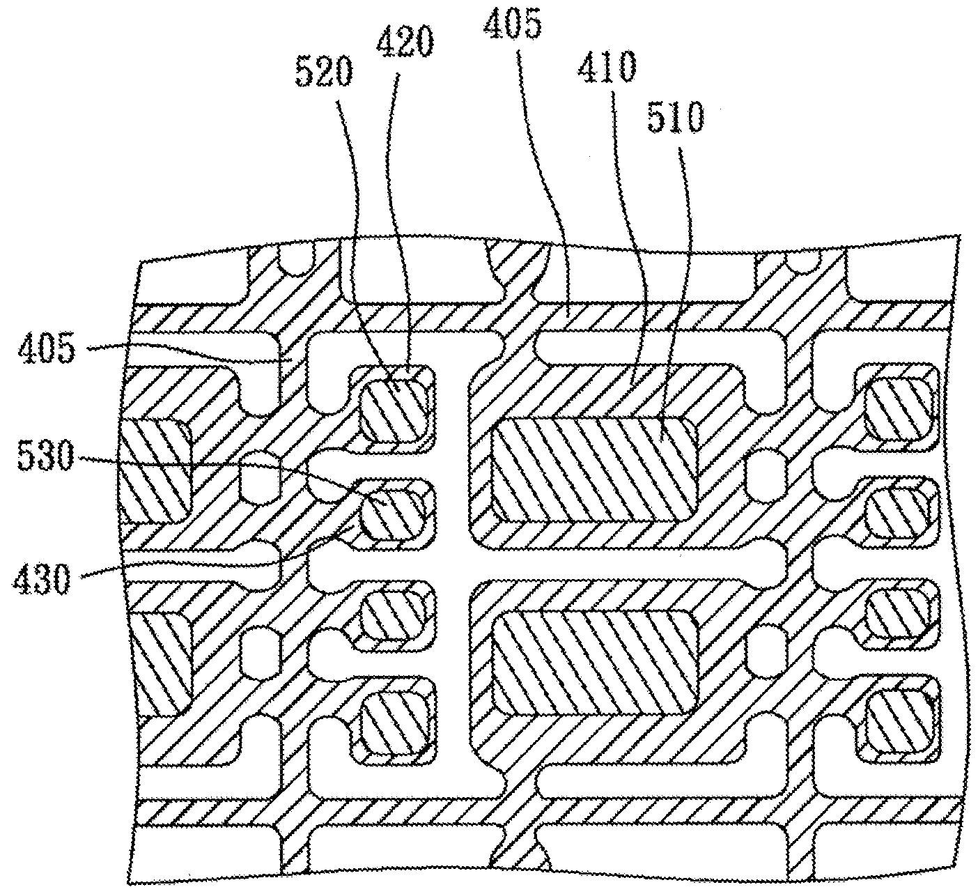
[0057] Figure 8 is an isometric view of the stack die package 400 in accordance with various embodiments of the invention. The present embodiment of the stack die package 400 illustrates exemplary shapes and orientations of selected different internal components of the stack die package 400. For example, Figure 8 illustrates exemplary shapes and orientations for the clips 416, 420a, and 420b, the upper die 418, the lower die 4 4, the lead frame 402, and the SL lead 408 and the GL lead 406 of the lead frame 402.
[0058] It is noted that the stack die package 400 may not include all of the elements illustrated by Figure 8. In addition, the stack die package 400 can be implemented to include one or more elements not illustrated by Figure 8. It is pointed out that the stack die package 400 can be utilized or implemented in any manner similar to that described herein, but is not limited to such.
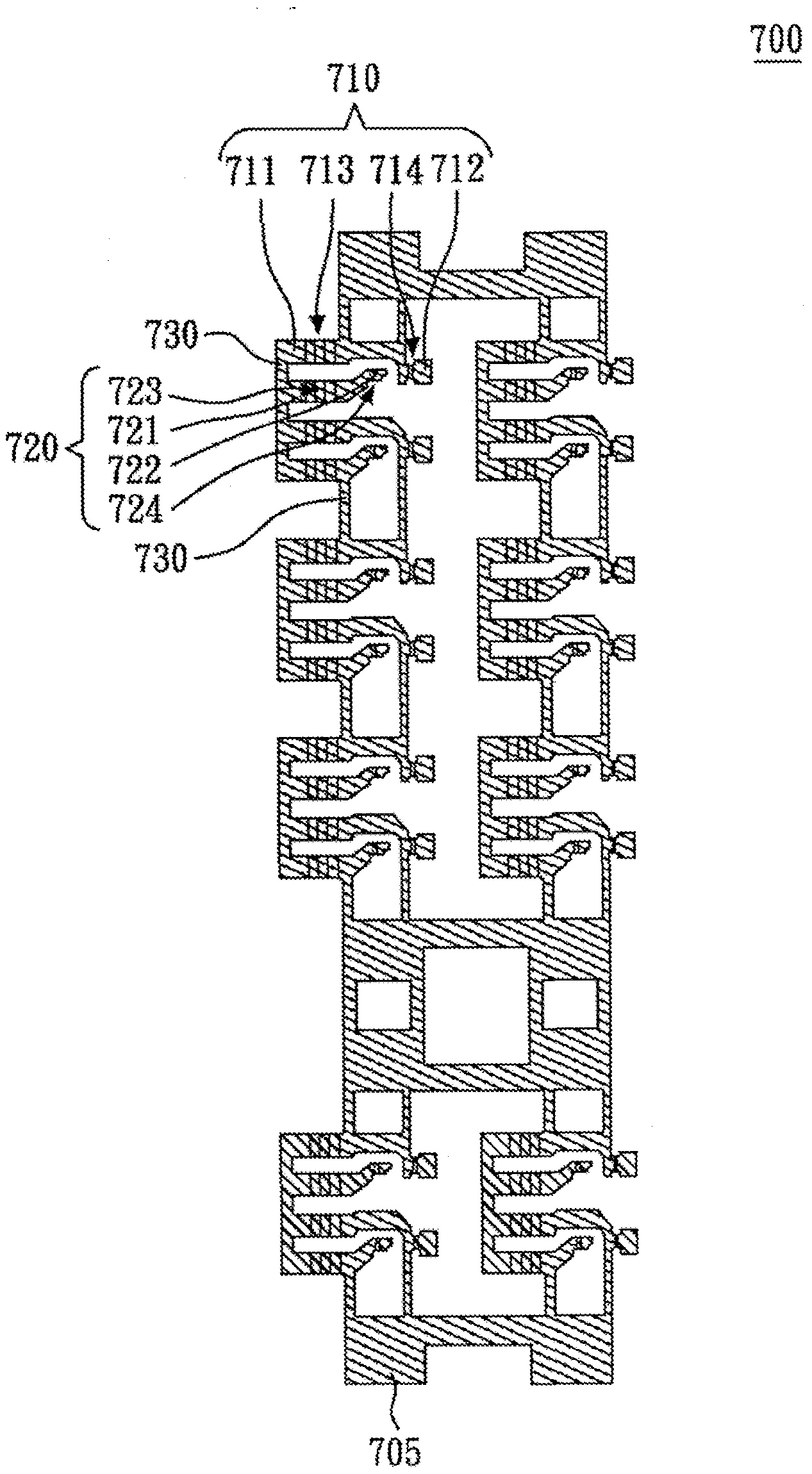
[0059] Figure 9 is an assembly process view of multiple stack dies (e.g., 400) in accordance with various embodiments of the invention. For example, the present embodiment of Figure 9 illustrates the lead frame 402 (e.g., which is a one piece frame) having multiple lower dies 414 situated above the lead frame 402. In addition, multiple clips 416 are shown that can be individually placed above each of the multiple lower dies 414. The present embodiment of Figure 9 also illustrates a frame clip 902 (e.g., which is a one piece frame) that includes, but is not limited to, eight sets of the clips 420a and 420b that are all coupled or connected together. In an embodiment, it is noted that the frame clip 902 can include tie bars that couple or connect together all the sets of clips 420a and 420b. In addition, in an embodiment, the frame clip 902 can include two larger ends 904 which can be utilized to pick up the frame clip 902 and position it and all the sets of clips 420a and 420b at the same time or approximately the same time above multiple upper dies 418 and multiple lower dies 414. It is noted that the frame clip 902 can be implemented to include any number of sets of the clips 420a and 420b (or the clips 616a and 616b), but is not limited to such. In an embodiment, the frame clip 902 can be fabricated of, but is not limited to, one or more electrically conductive materials (e.g., one or more metals, such as copper).
[0060] It is noted that the frame clip 902 may not include all of the elements illustrated by Figure 9. In addition, the frame clip 902 can be implemented to include one or more elements not illustrated by Figure 9. It is pointed out that the frame clip 902 can be utilized or implemented in any manner similar to that described herein, but is not limited to such.
[0061] Figure 10 is an isometric view of the stack die package 600 in accordance with various embodiments of the invention. The present embodiment of the stack die package 600 illustrates exemplary shapes and orientations of selected different internal components of the stack die package 600. For example, Figure 10 illustrates
exemplary shapes and orientations for the clips 620, 616a, and 616b, the upper die 618, the lower die 614, the lead frame 602, and the SL lead 608 and the GL lead 606 of the lead frame 602. [0062] It is noted that the stack die package 600 may not include all of the elements illustrated by Figure 10. In addition, the stack die package 600 can be implemented to include one or more elements not illustrated by Figure 10. It is pointed out that the stack die package 600 can be utilized or implemented in any manner similar to that described herein, but is not limited to such.
[0063] Figure 1 1 is an exploded view of the stack die package 600 in accordance with various embodiments of the invention. The present embodiment of the stack die package 600 illustrates exemplary shapes and orientations of selected different internal components of the stack die package 600. For example, Figure 11 illustrates
exemplary shapes and orientations for the clips 620, 616a, and 616b, the upper die 618, the lower die 614, the lead frame 602, and the SL lead 608 and the GL lead 606 of the lead frame 602.
[0064] It is noted that the stack die package 600 may not include all of the elements illustrated by Figure 11. In addition, the stack die package 600 can be implemented to include one or more elements not illustrated by Figure 11. It is pointed out that the stack die package 600 can be utilized or implemented in any manner similar to that described herein, but is not limited to such.
[0065] Figure 12 is a flow diagram of a method 1200 for fabricating one or more stack die packages in accordance with various embodiments of the invention. Although specific operations are disclosed in Figure 12, such operations are examples. The method 1200 may not include all of the operations illustrated by Figure 12. Also, method 1200 may include various other operations and/or variations of the operations shown. Likewise, the sequence of the operations of flow diagram 1200 can be modified. It is appreciated that not all of the operations in flow diagram 1200 may be performed. In various embodiments, one or more of the operations of method 1200 can be controlled or managed by software, by firmware, by hardware or by any combination thereof, but is not limited to such. Method 1200 can include processes of embodiments of the invention which can be controlled or managed by a processors) and electrical components under the control of computer or computing device readable and executable instructions (or code). The computer or computing device readable and executable instructions (or code) may reside, for example, in data storage features such as computer or computing device usable volatile memory, computer or computing device usable non-volatile memory, and/or computer or computing device usable mass data storage. However, the computer or computing device readable and executable instructions (or code) may reside in any type of computer or computing device readable medium or memory.
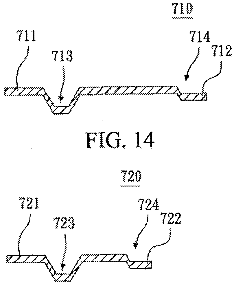
[0066] At operation 1202 of Figure 12, solder paste (e.g., 428) or epoxy can be deposited onto a lead frame (e.g., 402). It is noted that operation 1202 can be implemented in a wide variety of ways. For example, in one embodiment, Figure 13 illustrates a side sectional view of solder paste 428 (or epoxy) dispensed or printed onto the leads 404, 406, 408, 410, and 412 of the lead frame 402 at operation 1202, but is not limited to such. Operation 1202 can be implemented in any manner similar to that described herein, but is not limited to such.
[0067] At operation 1204, a first die or chip (e.g., 414) can be coupled or attached to the lead frame. Note that operation 1204 can be implemented in a wide variety of ways. For example, in an embodiment, Figure 14 illustrates the gate contact 436 and source contact 440 of the lower die 414 coupled or attached to the leads 406 and 408, respectively, of the lead frame 402 at operation 1204 utilizing a flip chip on lead frame technique, but is not limited to such. In one embodiment, at operation 1204, the lower die 414 can be picked up from the wafer, flipped over, and placed onto the solder paste 428 (or epoxy) previously deposited onto the lead frame 402 at operation 1202.
Operation 1204 can be implemented in any manner similar to that described herein, but is not limited to such.
[0068] At operation 1206 of Figure 12, solder paste (e.g., 426) or epoxy can be deposited onto the back side of the first die or chip. It is pointed out that operation 1206 can be implemented in a wide variety of ways. For example, in an embodiment, Figure 15 illustrates the solder paste 426 (or epoxy) dispensed or printed onto the drain contact 438 (e.g., back side) of the lower die 414 at operation 1206, but is not limited to such. Operation 1206 can be implemented in any manner similar to that described herein, but is not limited to such. [0069] At operation 1208, a first clip (e.g., 4 6) can be coupled or attached to the first die and the lead frame. Note that operation 1208 can be implemented in a wide variety of ways. For example, in an embodiment, Figure 16 illustrates the clip 416 coupled or attached to the lower die 414 via the solder paste 426 (or epoxy) and the lead 404 of the lead frame 402 via the solder paste 428 (or epoxy) at operation 1208. Operation 1208 can be implemented in any manner similar to that described herein, but is not limited to such.
[0070] At operation 1210 of Figure 12, solder paste (e.g., 424) or epoxy can be deposited on the first clip. It is noted that operation 1210 can be implemented in a wide variety of ways. For example, in an embodiment, Figure 17 illustrates the solder paste 424 (or epoxy) dispensed or printed onto the clip 416 at operation 1210, but is not limited to such. Operation 1210 can be implemented in any manner similar to that described herein, but is not limited to such.
[0071] At operation 1212, a second die or chip (e.g., 418) can be coupled or attached to the first clip. It is pointed out that operation 1212 can be implemented in a wide variety of ways. For example, in an embodiment, Figure 18 illustrates the upper die 418 coupled or attached to the clip 416 via the solder paste 424 (or epoxy) at operation 1212, but is not limited to such. Operation 1212 can be implemented in any manner similar to that described herein, but is not limited to such. [0072] At operation 1214 of Figure 12, solder paste (e.g., 422) or epoxy can be deposited onto the second die. Note that operation 1214 can be implemented in a wide variety of ways. For example, in an embodiment, Figure 19 illustrates the solder paste 422 (or epoxy) dispensed or printed onto the drain contact 430 and the gate contact 434 of the upper die 418 at operation 1214, but is not limited to such. Operation 1214 can be implemented in any manner similar to that described herein, but is not limited to such.
[0073] At operation 1216, a second clip (e.g., 420a) and a third clip (e.g., 420b) can be coupled or attached to the second die and the lead frame. It is noted that operation 1216 can be implemented in a wide variety of ways. For example, in one embodiment, Figure 20 illustrates the second clip 420a coupled or attached to the drain contact 430 of the upper die 418 via solder paste 422 (or epoxy) and the lead 412 of the lead frame 402 via solder paste 428 (or epoxy) at operation 1216. In addition, Figure 20 illustrates the third clip 420b coupled or attached to the gate contact 434 of the upper die 418 via the solder paste 422 (or epoxy) and the lead 410 of the lead frame 402 via solder paste 428 (or epoxy) at operation 1216. In an embodiment, it is pointed out that at operation 1216, the second and third clips can be coupled or attached to the second die and the lead frame at the same time or approximately the same time (e.g., utilizing a clip frame similar to the clip frame 902). Operation 1216 can be implemented in any manner similar to that described herein, but is not limited to such. [0074] At operation 1218 of Figure 12, a reflow process can be performed on the existing stack die assembly (e.g., as shown in Figure 20). It is pointed out that operation 1218 can be implemented in a wide variety of ways. For example, in an embodiment, the reflow process at operation 1218 can be implemented by increasing the temperature (e.g., greater than 350° C or greater than 370° C) of the stack die assembly, but is not limited to such. Note that under these conditions, in one embodiment, flux can be removed from the solder paste and when the temperature decreases, the solder can bond with the joints. In an embodiment, the operation 1218 can be implemented to include a cleaning process that occurs after the reflow process. Operation 1218 can be implemented in any manner similar to that described herein, but is not limited to such.
[0075] At operation 1220, the stack die assembly can be covered or encapsulated by a molding compound or material. Note that operation 1220 can be implemented in a wide variety of ways. For example, in an embodiment, Figure 21 illustrates a molding compound or material 442 covering or encapsulating the stack die assembly at operation 1220, but is not limited to such. Operation 1220 can be implemented in any manner similar to that described herein, but is not limited to such.
[0076] At operation 1222 of Figure 12, a package sawing process or operation can be performed on the stack die assembly covered with the molding compound or material. It is noted that operation 1222 can be implemented in a wide variety of ways. For example, in an embodiment, Figure 22 illustrates the occurrence of a package sawing process at operation 1222 resulting in the stack die package having, but not limited to, substantially vertical surfaces located near the leads 404 and 412 of the lead frame 404. In one embodiment, the package sawing process can automatically cut tie bars (e.g., 904) that were coupling the second clip (e.g., 420a) and the third clip (e.g., 420b).
Consequently, the second clip and the third clip are separated, become functional, and are held in place by the molding (e.g., 442). Operation 1222 can be implemented in any manner similar to that described herein, but is not limited to such.
[0077] At operation 1224, electrical testing can be performed on the stack die package to determine whether it operates properly. It is pointed out that operation 1224 can be implemented in a wide variety of ways. For example, operation 1224 can be
implemented in any manner similar to that described herein, but is not limited to such.
[0078] At operation 1226 of Figure 12, tape and reel can be performed on the stack die package. Note that operation 1226 can be implemented in a wide variety of ways. For example, in an embodiment, the tape and reel at operation 1226 can include putting the stack die package into packing material to protect it during transportation to a desired location. Operation 1226 can be implemented in any manner similar to that described herein, but is not limited to such.
[0079] In various embodiments, it is noted that one or more of the solder pastes described herein can instead be implemented with a conductive epoxy or conductive adhesive, but are not limited to such. In addition, in an embodiment, operation 1218 may not be performed if solder paste is not utilized during method 1200.
[0080] It is pointed out that even though method 1200 was described with reference to fabricating a single stack die package, method 1200 can be modified in accordance with various embodiments of the invention to fabricate multiple stack die packages at substantially the same time.
[0081] Figure 23 is a flow diagram of a method 2300 for fabricating one or more stack die packages in accordance with various embodiments of the invention. Although specific operations are disclosed in Figure 23, such operations are examples. The method 2300 may not include all of the operations illustrated by Figure 23. Also, method 2300 may include various other operations and/or variations of the operations shown. Likewise, the sequence of the operations of flow diagram 2300 can be modified. It is appreciated that not all of the operations in flow diagram 2300 may be performed. In various embodiments, one or more of the operations of method 2300 can be controlled or managed by software, by firmware, by hardware or by any combination thereof, but is not limited to such. Method 2300 can include processes of embodiments of the invention which can be controlled or managed by a processor(s) and electrical components under the control of computer or computing device readable and executable instructions (or code). The computer or computing device readable and executable instructions (or code) may reside, for example, in data storage features such as computer or computing device usable volatile memory, computer or computing device usable non-volatile memory, and/or computer or computing device usable mass data storage. However, the computer or computing device readable and executable instructions (or code) may reside in any type of computer or computing device readable medium or memory.
[0082] At operation 2302 of Figure 23, solder paste (e.g., 628) or epoxy can be deposited onto a lead frame (e.g., 602). It is noted that operation 2302 can be implemented in a wide variety of ways. For example, in an embodiment, Figure 24 illustrates a side sectional view of solder paste 628 (or epoxy) dispensed or printed onto the leads 604, 606, 608, 610, and 612 of the lead frame 602 at operation 2302, but is not limited to such. Operation 2302 can be implemented in any manner similar to that described herein, but is not limited to such.
[0083] At operation 2304, a first die or chip (e.g., 614) can be coupled or attached to the lead frame. Note that operation 2304 can be implemented in a wide variety of ways. For example, in an embodiment, Figure 25 illustrates the gate contact 636 and source contact 640 of the lower die 614 coupled or attached to the leads 606 and 608, respectively, of the lead frame 602 at operation 2304 utilizing a flip chip on lead frame technique, but is not limited to such. In one embodiment, at operation 2304, the lower die 614 can be picked up from the wafer, flipped over, and placed onto the solder paste 628 (or epoxy) previously deposited onto the lead frame 602. Operation 2304 can be implemented in any manner similar to that described herein, but is not limited to such. [0084] At operation 2306 of Figure 23, solder paste (e.g., 626) or epoxy can be deposited onto the back side of the first die or chip. It is pointed out that operation 2306 can be implemented in a wide variety of ways. For example, in an embodiment, Figure 26 illustrates the solder paste 626 (or epoxy) dispensed or printed onto the drain contact 638 (e.g., back side) of the lower die 614 at operation 2306, but is not limited to such. Operation 2306 can be implemented in any manner similar to that described herein, but is not limited to such.
[0085] At operation 2308, a first clip (e.g., 616a) and a second clip (e.g., 616b) can be coupled or attached to the lead frame while the first clip is also coupled or attached to the first die. It is noted that operation 2308 can be implemented in a wide variety of ways. For example, in an embodiment, Figure 27 illustrates the first clip 616a and the second clip 616b coupled or attached to the leads 604 and 610, respectively, of the lead frame 602 via solder paste 628 (or epoxy) while the first clip 616a is also coupled or attached to the drain contact 638 of the first die 614 via solder 626 (or epoxy) at operation 2308. In an embodiment, it is pointed out that at operation 2308, the first and second clips can be coupled or attached to the lead frame while the first clip can also be coupled or attached to the first die at the same time or approximately the same time (e.g., utilizing a clip frame similar to the clip frame 902). Operation 2308 can be implemented in any manner similar to that described herein, but is not limited to such.
[0086] At operation 2310 of Figure 23, solder paste (e.g., 624) or epoxy can be deposited on the first and second clips. It is noted that operation 2310 can be implemented in a wide variety of ways. For example, in an embodiment, Figure 28 illustrates the solder paste 624 (or epoxy) dispensed or printed onto the clips 616a and 616b at operation 2310, but is not limited to such. Operation 2310 can be implemented in any manner similar to that described herein, but is not limited to such.
[0087] At operation 2312, a second die or chip (e.g., 618) can be coupled or attached to the first and second clips. It is pointed out that operation 2312 can be implemented in a wide variety of ways. For example, in an embodiment, Figure 29 illustrates the source contact 632 of the upper die 618 coupled or attached to the clip 616a via the solder paste 624 (or epoxy) and the gate contact 634 of the upper die 618 coupled or attached to the clip 616b via the solder paste 624 (or epoxy) at operation 2312, but is not limited to such. Operation 2312 can be implemented in any manner similar to that described herein, but is not limited to such.
[0088] At operation 2314 of Figure 23, solder paste (e.g., 622) or epoxy can be deposited onto the second die. Note that operation 2314 can be implemented in a wide variety of ways. For example, in an embodiment, Figure 30 illustrates the solder paste 622 (or epoxy) dispensed or printed onto the drain contact 630 of the upper die 618 at operation 2314, but is not limited to such. Operation 2314 can be implemented in any manner similar to that described herein, but is not limited to such.
[0089] At operation 2316, a third clip (e.g., 620) can be coupled or attached to the second die and the lead frame. Note that operation 2316 can be implemented in a wide variety of ways. For example, in an embodiment, Figure 31 illustrates the clip 620 coupled or attached to the drain contact 630 of the upper die 614 via the solder paste 622 (or epoxy) and the lead 612 of the lead frame 602 via the solder paste 628 (or epoxy) at operation 2316. Operation 2316 can be implemented in any manner similar to that described herein, but is not limited to such.
[0090] At operation 2318 of Figure 23, a reflow process can be performed on the existing stack die assembly (e.g., as shown in Figure 31 ). It is pointed out that operation 2318 can be implemented in a wide variety of ways. For example, in an embodiment, the reflow process at operation 2318 can be implemented by increasing the temperature (e.g., greater than 350° C or greater than 370° C) of the stack die assembly, but is not limited to such. It is noted that under these conditions, in one embodiment, flux can be removed from the solder paste and when the temperature decreases, the solder can bond with the joints. In an embodiment, the operation 2318 can be implemented to include a cleaning process that occurs after the reflow process. Operation 2318 can be implemented in any manner similar to that described herein, but is not limited to such.
[0091] At operation 2320, the stack die assembly can be covered or encapsulated by a molding compound or material. It is pointed out that operation 2320 can be implemented in a wide variety of ways. For example, in an embodiment, Figure 32 illustrates a molding compound or material 642 covering or encapsulating the stack die assembly at operation 2320, but is not limited to such. Operation 2320 can be implemented in any manner similar to that described herein, but is not limited to such.
[0092] At operation 2322 of Figure 23, a package sawing process or operation can be performed on the stack die assembly covered with the molding compound or material. It is noted that operation 2322 can be implemented in a wide variety of ways. For example, in an embodiment, Figure 33 illustrates the occurrence of a package sawing process at operation 2322 resulting in the stack die package having, but not limited to, substantially vertical surfaces located near the leads 604 and 612 of the lead frame 604. In one embodiment, the package sawing process can automatically cut tie bars (e.g., 904) that were coupling the first clip (e.g., 616a) and the second clip (e.g., 616b).
Consequently, the first clip and the second clip are separated, become functional, and are held in place by the molding (e.g., 642). Operation 2322 can be implemented in any manner similar to that described herein, but is not limited to such.
[0093] At operation 2324, electrical testing can be performed on the stack die package to determine whether it operates properly. It is pointed out that operation 2324 can be implemented in a wide variety of ways. For example, operation 2324 can be
implemented in any manner similar to that described herein, but is not limited to such.
[0094] At operation 2326 of Figure 23, tape and reel can be performed on the stack die package. Note that operation 2326 can be implemented in a wide variety of ways. For example, in an embodiment, the tape and reel at operation 2326 can include putting the stack die package into packing material to protect it during transportation to a desired location. Operation 2326 can be implemented in any manner similar to that described herein, but is not limited to such.
[0095] In various embodiments, it is noted that one or more of the solder pastes described herein can instead be implemented with a conductive epoxy or conductive adhesive, but are not limited to such. In addition, in an embodiment, operation 2318 may not be performed if solder paste is not utilized during method 2300.
[0096] It is pointed out that even though method 2300 was described with reference to fabricating a single stack die package, method 2300 can be modified in accordance with various embodiments of the invention to fabricate multiple stack die packages at substantially the same time.
[0097] Figure 34 is a flow diagram of a method 3400 for fabricating one or more "double cooling" stack die packages in accordance with various embodiments of the invention. Although specific operations are disclosed in Figure 34, such operations are examples. The method 3400 may not include all of the operations illustrated by Figure 34. Also, method 3400 may include various other operations and/or variations of the operations shown. Likewise, the sequence of the operations of flow diagram 3400 can be modified. It is appreciated that not all of the operations in flow diagram 3400 may be performed. In various embodiments, one or more of the operations of method 3400 can be controlled or managed by software, by firmware, by hardware or by any combination thereof, but is not limited to such. Method 3400 can include processes of embodiments of the invention which can be controlled or managed by a processor(s) and electrical components under the control of computer or computing device readable and executable instructions (or code). The computer or computing device readable and executable instructions (or code) may reside, for example, in data storage features such as computer or computing device usable volatile memory, computer or computing device usable non-volatile memory, and/or computer or computing device usable mass data storage. However, the computer or computing device readable and executable instructions (or code) may reside in any type of computer or computing device readable medium or memory.
[0098] In an embodiment, it is noted that before performing method 3400, operations 1202-1218 of method 200 (Figure 12) may be performed as described herein. For example, in an embodiment, after completion of operation 1218 of Figure 12, method 3400 (Figure 34) can be performed as described below. Additionally, in one
embodiment, it is pointed out that before performing method 3400, operations 2302- 2318 of method 2300 (Figure 23) may be performed as described herein. For example, in an embodiment, after completion of operation 2318 of Figure 23, method 3400 (Figure 34) can be performed as described below.
[0099] At operation 3402, the stack die assembly (e.g., as shown in Figure 20 or Figure 31 ) can be covered or encapsulated by a molding compound or material except for at least a portion of a top or upper surface of an upper clip (e.g., 420a or 620) of the stack die assembly. After operation 3402, in an embodiment, at least a portion of the top surface of the upper clip can be free of the molding compound or material. It is noted that operation 3402 can be implemented in a wide variety of ways. For example, in an embodiment, Figure 35 illustrates a side sectional view of the stack die assembly of Figure 20 covered or encapsulating at operation 3402 by a molding compound or material 442a except for at least a portion of a top or upper surface of the upper clip 420a. In addition, in one embodiment, Figure 36 illustrates a side sectional view of the stack die assembly of Figure 31 covered or encapsulating at operation 3402 by a molding compound or material 642a except for at least a portion of a top or upper surface of the upper clip 620. Furthermore, Figure 7 illustrates the stack die package 600a that as part of its fabrication process, in an embodiment, could have been involved with the molding process of operation 3402 wherein the molding 642a covers or encapsulates the stack die assembly except for at least a portion of the top or upper surface of the upper clip 620.
[00100] In an embodiment, it is noted that a "double cooling" molding tool can be utilized at operation 3402 that has a lower cavity height than a molding tool typically utilized to completely encapsulate the stack die assembly as shown in Figure 21 or Figure 32. In addition, a top mold surface of the "double cooling" molding tool is capable of touching or contacting the top or upper surface of the upper clip (e.g., 420a or 620) of the stack die assembly at operation 3402. Furthermore, with a soft or flexible film located between the top mold and the upper surface of the clip at operation 3402, at least a portion of the upper surface of the clip can remain free of the molding compound while the remainder of the stack die assembly is covered or encompassed by the molding compound at operation 3402. In an embodiment, the molding process at operation 3402 can be referred to as Film Assisted Molding, but is not limited to such. Operation 3402 can be implemented in any manner similar to that described herein, but is not limited to such.
[00101] At operation 3404 of Figure 34, a determination can be made as to whether or not to plate the exposed top surface of the upper clip with one or more metals. If not, method 3400 can proceed to operation 3408. However, if it is determined at operation 3404 that the exposed top surface of the upper clip is to be plated with one or more metals, method 3400 can proceed to operation 3406. It is noted that operation 3404 can be implemented in a wide variety of ways. For example, in an embodiment, it may be decided at operation 3404 to plate the exposed top surface of the upper clip with one or more metals in order to later solder the upper surface of the clip to a heatsink.
Alternatively, in an embodiment, it may be decided at operation 3404 not to plate the exposed top surface of the upper clip with one or more metals since there is no desire to solder the upper surface of the clip to a heatsink. In addition, in an embodiment, it may be decided at operation 3404 not to plate the exposed top surface of the upper clip with one or more metals to avoid a later process (e.g., printed circuit board reflow process) from possibly melting the plating and obscuring laser markings implemented within the top surface (e.g., of the molding compound) of the stack die package.
Operation 3404 can be implemented in any manner similar to that described herein, but is not limited to such. [00102] At operation 3406, the exposed top surface of the clip of the stack die package can be plated with, but is not limited to, one or more metals (e.g., tin) to produce an exposed plated pad (e.g., 706). Note that operation 3406 can be implemented in a wide variety of ways. For example, in an embodiment, Figure 7 illustrates the top surface of the upper clip 620 tin-plated resulting in the formation of an exposed tin-plated pad 706 on the top surface of the upper clip 620. Operation 3406 can be implemented in any manner similar to that described herein, but is not limited to such. In this manner, the "double cooling" can be achieved by heat escaping the stack die package via its lead frame and heat escaping via its exposed plated pad.
[00103] At operation 3408 of Figure 34, the exposed top surface of the upper clip of the stack die package is prevented from being plated during a plating process (e.g., using one or more metals) of the stack die package. It is pointed out that operation 3408 can be implemented in a wide variety of ways. For example, in an embodiment, a film can be applied on or over the top side of the stack die package at operation 3408 to prevent the exposed top surface of the upper clip from being plated during a plating process of the stack die package. Operation 3408 can be implemented in any manner similar to that described herein, but is not limited to such.
[00104] In an embodiment, it is noted that after performing operation 3406 or 3408 of method 3400, operations 1222-1226 of method 1200 (Figure 2) may be performed as described herein. Furthermore, in one embodiment, note that after performing operation 3406 or 3408 of method 3400, operations 2322-2326 of method 2300 (Figure 23) may be performed as described herein.
[00105] It is pointed out that even though method 3400 of Figure 34 was described with reference to fabricating a single "double cooling" stack die package, method 3400 can be modified in accordance with various embodiments of the invention to fabricate multiple "double cooling" stack die packages at substantially the same time.
[00106] Figure 37 is a flow diagram of a method 3700 for fabricating one or more stack die packages in accordance with various embodiments of the invention. Although specific operations are disclosed in Figure 37, such operations are examples. The method 3700 may not include all of the operations illustrated by Figure 37. Also, method 3700 may include various other operations and/or variations of the operations shown. Likewise, the sequence of the operations of flow diagram 3700 can be modified. It is appreciated that not all of the operations in flow diagram 3700 may be performed. In various embodiments, one or more of the operations of method 3700 can be controlled or managed by software, by firmware, by hardware or by any combination thereof, but is not limited to such. Method 3700 can include processes of embodiments of the invention which can be controlled or managed by a processors) and electrical components under the control of computer or computing device readable and executable instructions (or code). The computer or computing device readable and executable instructions (or code) may reside, for example, in data storage features such as computer or computing device usable volatile memory, computer or computing device usable non-volatile memory, and/or computer or computing device usable mass data storage. However, the computer or computing device readable and executable instructions (or code) may reside in any type of computer or computing device readable medium or memory.
[00107] At operation 1202 of Figure 37, solder paste (e.g., 428) or epoxy can be deposited onto a lead frame (e.g., 402). It is noted that operation 1202 can be implemented in a wide variety of ways. For example, in one embodiment, Figure 38 illustrates a side sectional view of solder paste 428 (or epoxy) dispensed or printed onto the leads 404, 406, and 408 of the lead frame 402 at operation 1202, but is not limited to such. Note that at operation 1202, solder paste or epoxy can be deposited onto one or more of the leads (e.g., 404-412) of a lead frame (e.g., 402). Operation 1202 can be implemented in any manner similar to that described herein, but is not limited to such.
[00108] In an embodiment, it is noted that after performing operation 1202 of method 3700, operations 1204-1212 of method 3700 may be performed as described herein with reference to Figure 12, but are not limited to such.
[00109] At operation 3702 of Figure 37, the second die or chip (e.g., 418) can be coupled or attached to the lead frame. It is pointed out that operation 3702 can be implemented in a wide variety of ways. For example, in an embodiment, Figure 39 illustrates a wire 3904 coupled or attached to the drain contact 430 of the upper die 418 and the lead 412 of the lead frame 402 at operation 3702. In addition, Figure 39 illustrates a wire 3902 coupled or attached to the gate contact 434 of the upper die 418 and the lead 410 of the lead frame 402 at operation 3702. In an embodiment, it is pointed out that at operation 3702, the wires 3902 and 3904 can be coupled or attached to the second die and the lead frame via wire bonding, but are not limited to such. In an embodiment, note that the second die or chip can be coupled or attached to the lead frame at operation 3702 utilizing, but not limited to, one or more wires, one or more clips, any combination of one or more wires and one or more clips, etc. Operation 3702 can be implemented in any manner similar to that described herein, but is not limited to such.
[00110] In an embodiment, note that after performing operation 3702 of method 3700, operations 1218-1226 of method 3700 may be performed as described herein with reference to Figure 12, but are not limited to such. It is pointed out that at operation 1222 of method 3700, a package sawing process or operation can be performed on the stack die assembly covered with the molding compound or material. It is noted that operation 1222 can be implemented in a wide variety of ways. For example, in an embodiment, Figure 40 illustrates the occurrence of a package sawing process at operation 1222 resulting in the stack die package having, but not limited to, substantially vertical surfaces located near the leads 404 and 4 2 of the lead frame 402. Operation 1222 can be implemented in any manner similar to that described herein, but is not limited to such. [00111] It is pointed out that even though method 3700 of Figure 37 was described with reference to fabricating a single stack die package, method 3700 can be modified in accordance with various embodiments of the invention to fabricate multiple stack die packages at substantially the same time.
[00112] Figure 41 is a flow diagram of a method 4100 for fabricating one or more stack die packages in accordance with various embodiments of the invention. Although specific operations are disclosed in Figure 41 , such operations are examples. The method 4100 may not include all of the operations illustrated by Figure 41. Also, method 4100 may include various other operations and/or variations of the operations shown. Likewise, the sequence of the operations of flow diagram 4100 can be modified. It is appreciated that not all of the operations in flow diagram 4100 may be performed. In various embodiments, one or more of the operations of method 4100 can be controlled or managed by software, by firmware, by hardware or by any combination thereof, but is not limited to such. Method 4100 can include processes of embodiments of the invention which can be controlled or managed by a processor(s) and electrical components under the control of computer or computing device readable and executable instructions (or code). The computer or computing device readable and executable instructions (or code) may reside, for example, in data storage features such as computer or computing device usable volatile memory, computer or computing device usable non-volatile memory, and/or computer or computing device usable mass data storage. However, the computer or computing device readable and executable instructions (or code) may reside in any type of computer or computing device readable medium or memory.
[00113] At operation 2302 of Figure 41 , solder paste (e.g., 628) or epoxy can be deposited onto a lead frame (e.g., 602). It is noted that operation 2302 can be implemented in a wide variety of ways. For example, in one embodiment, Figure 42 illustrates a side sectional view of solder paste 628 (or epoxy) dispensed or printed onto the leads 604, 606, 608, and 610 of the lead frame 602 at operation 2302, but is not limited to such. Note that at operation 2302, solder paste or epoxy can be deposited onto one or more of the leads (e.g., 604-612) of a lead frame (e.g., 602). Operation 2302 can be implemented in any manner similar to that described herein, but is not limited to such.
[00114] In an embodiment, it is noted that after performing operation 2302 of method 4100, operations 2304-2312 of method 4100 may be performed as described herein with reference to Figure 23, but are not limited to such.
[00115] At operation 4102 of Figure 41 , the second die or chip (e.g., 618) can be coupled or attached to the lead frame. It is pointed out that operation 4102 can be implemented in a wide variety of ways. For example, in an embodiment, Figure 43 illustrates a wire 4302 coupled or attached to the drain contact 630 of the upper die 618 and the lead 612 of the lead frame 602 at operation 4102. In an embodiment, it is pointed out that at operation 4102, the wire 4302 can be coupled or attached to the second die and the lead frame via wire bonding, but is not limited to such. In an embodiment, note that the second die or chip can be coupled or attached to the lead frame at operation 4102 utilizing, but not limited to, one or more wires, one or more clips, any combination of one or more wires and one or more clips, etc. Operation 4102 can be implemented in any manner similar to that described herein, but is not limited to such.
[00116] In an embodiment, note that after performing operation 4102 of method 4100, operations 2318-2326 of method 4100 may be performed as described herein with reference to Figure 23, but are not limited to such. It is pointed out that at operation 2322 of method 3700, a package sawing process or operation can be performed on the stack die assembly covered with the molding compound or material. It is noted that operation 2322 can be implemented in a wide variety of ways. For example, in an embodiment, Figure 44 illustrates the occurrence of a package sawing process at operation 2322 resulting in the stack die package having, but not limited to, substantially vertical surfaces located near the leads 604 and 612 of the lead frame 602. Operation 2322 can be implemented in any manner similar to that described herein, but is not limited to such.
[00117] It is pointed out that even though method 4100 of Figure 41 was described with reference to fabricating a single stack die package, method 4100 can be modified in accordance with various embodiments of the invention to fabricate multiple stack die packages at substantially the same time. [00118] In various embodiments, it is noted that one or more of the solder pastes described herein can instead be implemented with a conductive epoxy or conductive adhesive, but are not limited to such.
[00119] The foregoing descriptions of various specific embodiments in accordance with the invention have been presented for purposes of illustration and description. They are not intended to be exhaustive or to limit the invention to the precise forms disclosed, and many modifications and variations are possible in light of the above teaching. The invention is to be construed according to the Claims and their equivalents.
[00120] All elements, parts and steps described herein are preferably included. It is to be understood that any of these elements, parts and steps may be replaced by other elements, parts and steps or deleted altogether as will be obvious to those skilled in the art.
[00121] CONCEPTS
The foregoing description presents at least the following concepts.
Concept 1 . A stack die package comprising:
a lead frame; a first die comprising a gate and a source that are located on a first surface of said first die and a drain that is located on a second surface of said first die that is opposite said first surface, said gate and source being flip chip coupled to said lead frame; and
a second die comprising a gate and a drain that are located on a first surface of said second die and a source that is located on a second surface of said second die that is opposite said first surface, said source of said second die facing said drain of said first die.
Concept 2. The stack die package of Concept 1 , further comprising:
a clip coupled to said lead frame and said gate of said second die.
Concept 3. The stack die package of Concept 1 or 2, further comprising:
a clip coupled to said lead frame and said drain of said second die.
Concept 4. The stack die package of Concept 3, further comprising:
a molding material covering said first die, second die, and clip while a portion of an upper surface of said clip is free of said molding material.
Concept 5. The stack die package of Concept 1 , further comprising:
a first clip coupled to said lead frame, said drain of said first die, and said source of said second die. Concept 6. The stack die package of Concept 5, further comprising:
a second clip coupled to said lead frame and said gate of said second die.
Concept 7. The stack die package of Concept 5 or 6, further comprising:
a third clip coupled to said lead frame and said drain of said second die.
Concept 8. The stack die package of Concepts 1-7, wherein said first die comprises split gate technology.
Concept 9. The stack die package of Concepts 1-8, wherein said second die comprises Laterally Diffused Metal Oxide Semiconductor (LDMOS) technology.
Concept 10. A stack die package comprising:
a lead frame;
a first die comprising a gate and a source that are located on a first surface of said first die and a drain that is located on a second surface of said first die that is opposite said first surface, said gate and source being flip chip coupled to said lead frame; and
a second die comprising a gate and a source that are located on a first surface of said second die and a drain that is located on a second surface of said second die that is opposite said first surface, said source of said second die facing said drain of said first die. Concept 1 1. The stack die package of Concept 10, further comprising: a clip coupled to said lead frame and said gate of said second die.
Concept 12. The stack die package of Concept 10 or 11 , further comprising:
a clip coupled to said lead frame and said drain of said second die.
Concept 13. The stack die package of Concept 12, further comprising:
a molding material covering said first die, second die, and clip while a portion of an upper surface of said clip is free of said molding material.
Concept 14. The stack die package of Concept 10, further comprising:
a first clip coupled to said lead frame, said drain of said first die, and said source of said second die.
Concept 15. The stack die package of Concept 14, further comprising:
a second clip coupled to said lead frame and said gate of said second die.
Concept 16. The stack die package of Concept 14 or 15, further comprising:
a third clip coupled to said lead frame and said drain of said second die.
Concept 17. The stack die package of Concepts 10-16, wherein said first die comprising split gate technology. Concept 18. The stack die package of Concepts 10-17, wherein said second die comprising split gate technology.
DUAL LEAD FRAME SEMICONDUCTOR PACKAGE AND METHOD OF
MANUFACTURE
BACKGROUND OF THE IN VENTION
10001 j The manufacture of integrated circuits includes the packaging of the semiconductor chip. Figures 1 , 2 and 3 illustrate a conventional method for making a semiconductor package. Referring to Figure 1 , a lead frame is provided. The lead frame 1 includes at least one drain pin 1 1 , at leas one source pin 13 and at least one gate pin 14. The drain pin 1 1 , source pin 13 and gate pin are connected to the a frame (not shown) by corresponding extensions 12. The source pin 13 and the gate pin 14 face a side of the drain pin 1 1 , and a space exists between the source pin 13 and the side of the drain pin 1 1 and between the gate pin 14 and the side of the drain pin 1 1.
|0002| Referring now to Figure 2, at least one chip 2 is provided. The chip 2 has an upper surface 21 and a lower surface (not shown). The upper surface 21 has a source conductive region 22 and a gate conductive region 23. The lower surface has a drain conductive region (not shown). The chip 2 is disposed so that the drain conductive region is electrically connected to the drain pin 1 1.
10003) Referring now to Figure 3, a wiring process is performed. A first wire 31 is used to connect the source pin 13 of the lead frame 1 and the source conductive region 22 of the chip 2, and a second wire 32 is used to connect the gate pin 14 of the lead frame 1 and the
Appendix A -53- gate conductive region 23 of the chip 2. The method may then continue with a molding process and a cutting process to further form the semiconductor package.
|0004] The conventional method for making the semiconductor package has the following disadvantages. The first wire 31 and the second wire 32 are gold wires, so the material cost is high. Moreover, during the wire bonding process, a wiring machine is used to form the first wire 31 and the second wire 32 one by one, which is time consuming.
Further, a certain space must be reserved between the first wire 3 1 and the second wire 32 for the movement of a wiring head of the wiring machine, so that the space between the first wire 31 and the second wire 32 cannot be effectively narrowed. If the size of the chip 2 is reduced to a certain degree, the conventional method is not applicable.
|0005| Therefore, there is a continuing need to provide an improved
semiconductor package and a method for making the same, to solve the above problems.
Appendix A -54- SUMMARY OF THE INVENTION
|0006| The present technology may best be understood by referring to the following description and accompanying drawings that are used to illustrate embodiments of the present technology directed toward a semiconductor package and method for making the same. The techniques, in one or more embodiments, include a semiconductor package of a transistor without any wires and a method of making the same.
| 0007| In one embodiment a method of fabricating a semiconductor package includes providing a substrate lead frame, wherein the substrate lead frame comprises a substrate frame, at least one first substrate lead, at least one second substrate lead, and at least one third substrate lead, wherein the first substrate lead is connected to the substrate frame, the second substrate lead and the third substrate lead face a side of the first substrate lead, and wherein the second substrate lead has a first extension portion connected to the substrate frame, and the third substrate lead has a second extension portion connected to the substrate frame. At least one 1C chip is also provided, wherein the at least one IC chip has an upper surface and a lower surface, the upper surface has a second conductive region and a third conductive region, and the lower surface has a first conductive region. The at least one IC chip is disposed on the substrate frame, wherein the first conductive region is electrically connected to the at least one first substrate lead. A clip lead frame is also provided, wherein the clip lead frame comprises a clip frame, at least one first clip lead, and at least one second clip lead, wherein the at least one first clip lead is connected to the clip frame and the at least one second clip is connected to the clip frame. The clip lead frame is disposed on the at least
Appendix A -55- one IC chip, wherein the first clip lead is electrically connected to the second conductive region of the at least one IC chip, the second clip lead is electrically connected to the third conductive region of the at least one IC chip. A molding process is performed and then a cutting process is performed to remove to form at least one semiconductor package each including at least one IC chip.
[0008] In another embodiment, a semiconductor package Includes a substrate lead frame, at least one chip, a clip lead frame and molding compound. The substrate lead frame includes at least one substrate frame, at least one first substrate lead, at least one second substrate lead, and at least one third substrate lead, wherein the first substrate lead is connected to the substrate frame, the second substrate lead and the third substrate lead face a side of the first substrate lead, the second substrate lead has a first extension portion, and the third substrate lead has a second extension portion. The at least one chip are each located on the respective first substrate lead and having an upper surface and a lower surface, wherein the upper surface has a second conductive region and a third conductive region, the lower surface has a first conductive region, and the first conductive region is electrically connected to the first substrate lead. The clip lead frame is located on the at least one chip and having at least one first clip lead and at least one second clip lead, wherein the first clip lead is electrically connected to the second conductive region of the at least one chip and the second substrate lead respectively, and the second clip lead is electrically connected to the third conductive region of the at least one chip and the third substrate lead respectively. The molding compound encapsulates the substrate lead frame, the at least one chip, and the clip
Appendix A -56- lead frame, wherein the at least one first substrate lead, the at least one second substrate lead, the at least one third substrate lead are exposed to a side surface of the molding compound.
|0009J In yet another embodiment, a method of making a semiconductor package includes receiving a substrate lead frame including a plurality of substrate lead set portions and a substrate frame portion, wherein each substrate lead set includes a first substrate lead, a second substrate lead and a third substrate lead, and wherein each of the first substrate leads, second substrate leads and third substrate leads are coupled to the substrate frame portion by one or more substrate extensions. A plurality of IC chips are also received, wherein each IC chip includes a first conductive region on a first surface, and a second conductive region and a third conductive region on a second surface. Each of the plurality of IC chips are disposed on the first substrate lead. A clip lead frame is also received, the clip lead frame includes a plurality of clip lead set portions and a clip frame portion, wherein each clip lead set includes a first clip lead and a second clip lead, and wherein each of the first clip leads and second clip leads are coupled to the clip frame portion by one or more clip extensions. The clip lead frame is disposed on the plurality of IC chips, wherein each of the first clip leads is disposed between the second conductive region on a respective IC chip and the respective second substrate lead of the substrate lead frame and each of the second clip leads is disposed between the third conductive region on a respective IC chip and the respective third substrate lead of the substrate lead frame. The first substrate lead is coupled to the first conductive region of the respective IC chip. The first clip lead is coupled between the second conductive region on the respective IC chip and the second substrate lead. The second clip
Appendix A -57- lead is coupled between the third conductive region on the respective IC chip and the third substrate lead for each of the plurality of IC chips. The substrate lead frame, the plurality of IC chips and the clip lead frame are then encapsulated before cutting the lead frame, plurality of IC chips and clip lead frame in a plurality of predetermined locations to separate the first substrate leads, second substrate leads and third substrate leads from the substrate frame and the first clip leads and the second clip leads from the clip frame to form packages each including at least one IC chip including the first substrate lead coupled to the respective IC chip, the first clip lead coupled between the respective IC chip and second substrate lead, and second clip lead coupled between the respective IC chip and the third substrate lead.
|0010) This Summary is provided to introduce a selection of concepts in a simplified form that are further described below in the Detailed Description. This Summary is not intended to identify key features or essential features of the claimed subject matter, nor is it intended to be used to limit the scope of the claimed subject matter.
BRIEF DESCRIPTION OF THE DRAWINGS
[001 11 Embodiments of the present technology are illustrated by way of example and not by way of limitation, in the figures of the accompanying drawings and in which like reference numerals refer to similar elements and in which:
Figures 1 , 2 and 3 show a schematic view illustrating various stages of a method for making a semiconductor package, according to the conventional art.
Figures 4 through 23 show a schematic view illustrating various stages of a method for making a semiconductor package, in accordance with one embodiment of the present technology.
Appendix A -59- DETAILED DESCRIPTION OF THE INVENTION
[0012] Reference will now be made in detail to the embodiments of the present technology, examples of which are illustrated in the accompanying drawings. While the present technology will be described in conjunction with these embodiments, it will be understood that they are not intended to limit the invention to these embodiments. On the contrary, the invention is intended to cover alternatives, modifications and equivalents, which may be included within the scope of the invention as defined by the appended claims.
Furthermore, in the following detailed description of the present technology, numerous specific details are set forth in order to provide a thorough understanding of the present technology. However, it is understood that the present technology may be practiced without these specific details. In other instances, well-known methods, procedures, components, and circuits have not been described in detail as not to unnecessarily obscure aspects of the present technology.
(00131 In this application, the use of the disjunctive is intended to include the conjunctive. The use of definite or indefinite articles is not intended to indicate cardinality. In particular, a reference to "the" object or "a" object is intended to denote also one of a possible plurality of such objects. It is also to be understood that the phraseology and terminology used herein is for the purpose of description and should not be regarded as limiting.
Appendix A -60- [0014] Embodiments of the present technology are directed toward semiconductor packaging techniques. Referring now to Figure 4, a stage in the manufacture of a semiconductor package, in accordance with one embodiment of the present technology, is shown. The stage illustrated in Figure 4 will be further explained with reference to Figure 5, which is a partially enlarged view of Figure 4. Figures 4 and 5 illustrate a substrate lead frame 400 including a frame portion 405 and a plurality of lead set 410, 420, 430 portions. For each set of leads, a first substrate lead 410 is coupled to the frame portion 405 by one or more extensions 415. A second substrate lead 420 and a third substrate lead 430 are coupled to the frame portion 405 by one or more respective extensions 425, 435. The second substrate lead 420 and third substrate lead 430 are separated by a space from the first substrate lead 410 along a first side 41 1 of the first substrate lead 410. In one implementation, the first substrate lead 410 is a first drain interconnect, the second substrate lead 420 is a first source interconnect, and the third substrate lead 430 is a first gate interconnect. In another implementation, the first substrate lead 410 is a first source interconnect, the second substrate lead 420 is a first drain interconnect, and the third substrate lead 430 is a first gale interconnect.
|0015| Referring now to Figure 6, another stage in the manufacture of a semiconductor package, in accordance with one embodiment of the present technology, is shown. The stage illustrated in Figure 6 will be further explained with reference to Figure 7, which is a partially enlarged view of Figure 6. A first solder 510 is formed on the first
Appendix A -61- substrate lead 410, a second solder 520 is fonned on the second substrate lead 420, and a third solder 530 is formed on the third substrate lead 430.
|0016| Referring now to Figure 8, yet another stage in the manufacture of a semiconductor package, in accordance with one embodiment of the present technology, is shown. The stage illustrated in Figure 8 will be further explained with reference to Figure 9, which is a partially enlarged view of Figure 8. An integrated circuit (IC) chip 600 is disposed on the first substrate lead 410 of each set of leads of the substrate lead frame. In one implementation, the fC chip 600 is a power metal-oxide-semiconductor field-effect transistor (MOSFET). Each IC chip 600 has an upper surface 610 and a lower surface 640 ( not shown in Figures 8 and 9). The lower surface has a first conductive region (not shown in Figures 8 and 9) disposed on the first solder 520 on the first substrate lead 410 of the substrate lead frame 400. The upper surface 610 of the IC chip 600 has a second conductive region 620 and a third conductive region 630. In the one implementation, the first conductive region is a drain conductive region, the second conductive region 620 is a source conductive region, and the third conductive region 630 is a gate conductive region. In the other implementation, the first conductive region is a source conductive region, the second conductive region 620 is a drain conductive region, and the third conductive region 630 is a gate conductive region.
|0017| Referring now to Figure 10, yet another stage in the manufacture of a semiconductor package, in accordance with one embodiment of the present technology, is
Appendix A -62- shown. The stage illustrated in Figure 10 will be further explained with reference to Figure 1 1 , which is a partially enlarged view of Figure 10. As illustrated in Figures 10 and 1 1 , a fourth solder 540 is formed on the second conductive region 620 and a fifth solder 550 is formed on the third conductive region 630 of the 1C chip 600
[0018] Referring now to Figure 12, yet auodier stage in the manufacture of a semiconductor package, in accordance with one embodiment of the present technology, is shown. The stage illustrated in Figure 12 will be further explained with reference to Figures 13, 14 and 15. Figure 13 is a partially enlarged view of Figure 12. Figure 14 is a cross- sectional view of Figure 12 taken along line 14- 14, and Figure 1 5 is a cross-section viesv of Figure 12 taken along line 15-15. Figures 12- 15 illustrate a clip lead frame 700 including a frame portion 705 and a plurality of lead set 710, 720 portions. Each set of clip leads 710, 720 are coupled to the frame portion 705 by one or more respective extensions 730. In one implementation, the frame portion 705 includes one or more larger physical areas for providing an area required by absorption. In the one implementation, a first clip lead 710 is a second source interconnect, and a second clip lead 720 is a second gate interconnect. In the other implementation, the first clip lead 710 is a second drain interconnect, and the second clip lead 720 is a second gate interconnect.
|0019| Each of the first clip leads 7 10 includes a first end 71 1 , a second end 712, a first recess 713 and a second recess 714. Each of the second clip leads 720 includes a first end 721, a second end 722, a first recess 723, and a second recess 724.
r
Appendix A -63- |0020| Referring now to Figure 16, yet another stage in the manufacture of a semiconductor package, in accordance with one embodiment of the present technology, is shown. The stage illustrated in Figure 16 will be further explained with reference to Figures 17 and 18. Figure 17 is a partially enlarged view of Figure 16. Figure 18 is a cross-sectional view of Figure 16 taken along line 18- 18. Figures 16- 18 illustrate assembly of the substrate lead frame 400, the IC chips 600, and the clip lead frame 700. The first clip lead 710 is disposed at the first recess 712 on the second solder 520 on the second substrate lead 420, and the second end 712 of the first clip lead 710 is disposed on the fourth solder 540 on the second conductive region 620 of the IC chip 600. The second clip lead 720 is disposed at the first recess 724 on the third solder 530 on the third substrate lead 430, and the second end 722 of the second clip lead 720 is disposed on the fifth solder 550 on the third conductive region 630 of the IC chip 600.
|0021 ] A solder reflow process is performed to electrically and mechanically connect the clip leads 710, 720 of the clip lead frame 700, the IC chips 600 and the substrate leads 410, 420, 430 of the substrate lead frame 400 together. As a result, the first clip lead 710 is electrically and mechanically coupled at the first recess 712 to the second substrate lead 420, and the second end 712 of the first clip lead 710 is electrically and mechanically coupled to the second conductive region 620 of the IC chip 600. The second clip lead 720 at the first recess 724 is electrically and mechanically coupled to the third substrate lead 430, and the second end 722 of the second clip lead 720 is electrically and mechanically coupled to the third conductive region 630 of the IC chip 600.
Appendix A -64- |00221 Referring now to Figure 1 , yet another stage in the manufacture of a semiconductor package, in accordance with one embodiment of the present technology, is shown. In Figure 19 a molding process is performed. The substrate lead frame 400, the IC chips 600 and the clip lead frame 700 coupled together are placed in a mold cavity (not shown), and then a molding compound 800 is filled in the mold cavity to encapsulate the substrate lead frame 400, the IC chips 600 and the clip lead frame 700. In one implementation, the first, second and third substrate leads 410, 420, 430 are exposed outside the molding compound 800.
[0023] Referring now to Figures 20 and 21 , yet another stage in the manufacture of a semiconductor package, in accordance with one embodiment of the present technology, is shown. As illustrated in Figure 20, a cutting process may be performed along first cutting lines L 1 . As illustrated in Figure 21 , an alternative cutting process may be performed along second cutting lines L2. Cutting along lines LI or L2 separates the substrate leads 410, 420, 430 from the substrate frame 405 and from each other. Cutting along lines L I or L2 also separates the clip leads 710, 720 from the clip frame 705 and from each other. However, the second substrate lead 420 remains electrically and mechanically coupled to the first clip lead 7 10 and the third substrate lead 430 remains electrically and mechanically coupled to the second clip lead 720.
|0024| Referring now to Figures 22 and 23, yet another stage in the manufacture of a semiconductor package, in accordance with another embodiment of the present
Appendix A -65- technology, is shown. Figure 22 shows a top view of a semiconductor package 900 inside the molding compound. Figure 23 shows a side sectional view of the semiconductor package 900. Figure 22 illustrates the semiconductor package 900 including two IC chips 600 resulting from cutting along cut lines L2 in Figure 21.
[0025] The semiconductor package 900, in accordance with embodiments of the present invention includes one or more IC chips 400. A first conductive region on a first surface of a respective IC chip 400 is electrically and mechanically coupled to a first substrate lead 410. A first clip lead 710 is electrically and mechanically coupled between a second conductive region on the second surface of the respective IC chip 400 and a second substrate lead 420. A second clip lead 720 is electrically and mechanically coupled between a third conductive region on the second surface of the respective IC chip 400 and a third substrate lead 420. The one or more IC chips 400, the respective first, second and third substrate leads 410, 420, 430 and the first and second clip leads 710, 720 are encapsulated, except for package contact portions of the first, second and third substrate leads 410, 420, 430. In the one implementation, the first substrate lead 410 is a drain interconnect, the coupled together first clip lead 710 and second substrate lead 420 is a source interconnect, and the coupled together second clip lead 720 and third substrate lead 430 is a gate interconnect of the respective IC chip 400 within the package 900. In the other implementation, the first substrate lead 410 is a source interconnect, the coupled together first clip lead 710 and second substrate lead 420 is a drain interconnect, and the coupled
Appendix A -66- together second clip lead 720 and third substrate lead 430 is a gate interconnect of the
respective IC chip 400 within the package 900
[0026] Embodiments of the present technology are advantageously adaptable to manufacturing integrated circuit packages including one or more IC chips. Moreover, embodiments of the present technology do not utilize gold wires to may package interconnects, which effectively saves on material cosst. In addition, the whole clip lead frame 700 of the present technology is integrally placed to effectively save processing time. The clip lead frame 700 may be fabricated through etching or other sophisticated techniques to narrow a space between the clip leads 710, 720, so that the clip lead frame 700 is applicable to IC chips 600 having a small size.
|0027| The foregoing descriptions of specific embodiments of the present technology have been presented for purposes of illustration and description. They are not intended to be exhaustive or to limit the invention to the precise forms disclosed, and obviously many modifications and variations are possible in light of the above teaching. The embodiments were chosen and described in order to best explain the principles of the present technology and its practical application, to thereby enable others skilled in the art to best utilize the present technology and various embodiments with various modifications as are suited to the particular use contemplated. It is intended that the scope of the invention be defined by the claims appended hereto and their equivalents.
Appendix A -67- CLAIMS
What is claimed is:
1 . A method for making a semiconductor package, comprising:
(a) providing a substrate lead frame, wherein the substrate lead frame comprises a substrate frame, at least one first substrate lead, at least one second substrate lead, and at least one third substrate lead, wherein the first substrate lead is connected to the substrate frame, the second substrate lead and the third substrate lead face a side of the first substrate lead, and wherein die second substrate lead has a first extension portion connected to the substrate frame, and the third substrate lead has a second extension portion connected to the substrate frame;
(b) providing at least one 1C chip, wherein the at least one IC chip has an upper surface and a lower surface, the upper surface has a second conductive region and a third conductive region, and the lower surface has a first conductive region;
(c) disposing the at least one IC chip on the substrate frame, wherein the first conductive region is electrically connected to the at least one first substrate lead;
(d) providing a clip lead frame, wherein the clip lead frame comprises a clip frame, at least one first clip lead, and at least one second clip lead, wherein the at least one first clip lead is connected to the clip frame and the at least one second clip is connected to the clip frame;
(e) disposing the clip lead frame on the at least one IC chip, wherein the first clip lead is electrically connected to the second conductive region of the at least one IC chip, the second clip lead is electrically connected to the third conductive region of the at least one IC
Appendix A -68- chip;
(f) performing a molding process; and
(g) performing a cutting process to remove to form at least one semiconductor package each including at least one 1C chip.
2. The method according to claim 1 , wherein in the step (a), the substrate lead frame further comprises a plurality of fixed connection segments, for connecting the substrate frame, the at least one first substrate lead, the at least one second substrate lead, and the at least one third substrate lead.
3. The method according to claim 1 , wherein in the step (a), a space exists between the second substrate lead and the side of the first substrate lead and between the third substrate lead and the side of the first substrate lead.
4. The method according to claim 1 , wherein after the step (b), the method further comprises a step of forming a first solder on the first substrate lead, the second substrate lead, and the third substrate lead; after the step (c). the method further comprises a step of forming a second solder on the first clip lead and the second clip lead; and after the step (e), the method further comprises a step of performing a solder reflow process.
5. The method according to claim 1 , wherein in the step (d), the at least one first clip lead has a first end and a second end, the at least one second clip lead has a third end and a
Appendix A -69- fourth end, and both the second end of the at least one first clip lead and the fourth end of the at least one second clip lead are connected to the at least one intermediate connection segment; and in the step (e), the first end of the first clip lead is electrically connected to the second conductive region of the at least one chip, and the third end of the second clip lead is electrically connected to the third conductive region of the at least one chip.
6. The method according to claim 1 , wherein in the step (d), the at least one first clip lead has a first recess and a second recess, the at least one second clip lead has a third recess and a fourth recess, the at least one first clip lead is electrically connected to the second conductive region of the at least one chip through the first recess, the at least one first clip lead is electrically connected to the second substrate lead through the second recess, the second clip lead is electrically connected to the third conductive region of the at least one chip through the third recess, and the second clip lead is electrically connected to the third substrate lead through the fourth recess.
7. The method according to claim 1 , wherein the first substrate lead is a drain pin, die second substrate lead is a source pin, the third substrate lead is a gate pin, the first conductive region is a drain conductive region, the second conductive region is a source conductive region, the third conductive region is a gate conductive region, the first clip lead is a source connection segment, and the second clip lead is a gate connection segment.
Appendix A -70- 8. The method according to claim 1 , wherein the first substrate lead is a source pin, the second substrate lead is a drain pin, the third substrate lead is a gate pin, the first conductive region is a source conductive region, the second conductive region is a drain conductive region, the third conductive region is a gate conductive region, the first clip lead is a drain connection segment, and the second clip lead is a gate connection segment.
9. A semiconductor package, comprising:
a substrate lead frame, comprising at least one substrate frame, at least one first substrate lead, at least one second substrate lead, and at least one third substrate lead, wherein the first substrate lead is connected to the substrate frame, the second substrate lead and the third substrate lead face a side of the first substrate lead, the second substrate lead has a first extension portion, and the third substrate lead has a second extension portion;
at least one chip, each located on the respective first substrate lead and having an upper surface and a lower surface, wherein the upper surface has a second conductive region and a third conductive region, the lower surface has a first conductive region, and the first conductive region is electrically connected to the first substrate lead;
a clip lead frame, located on the at least one chip and having at least one first clip lead and at least one second clip lead, wherein the first clip lead is electrically connected to the second conductive region of the at least one chip and the second substrate lead respectively, and the second clip lead is electrically connected to the third conductive region of the at least one chip and the third substrate lead respectively; and
a molding compound, encapsulating the substrate lead frame, the at least one chip,
Appendix A -71 - and the clip lead frame, wherein the at least one first substrate lead, the at least one second substrate lead, the at least one third substrate lead are exposed to a side surface of the molding compound.
10. The semiconductor package according to claim 9, wherein a space exists between the second substrate lead and the side of the first substrate lead and between the third substrate lead and the side of the first substrate lead.
1 1 . The semiconductor package according to claim 9, further comprising:
a first solder, for connecting the at least one first substrate lead and the at least one chip, connecting the second substrate lead and the first clip lead, and connecting the third substrate lead and the second clip lead; and
a second solder, for connecting the first clip lead and the second conductive region of the at least one chip and connecting the second clip lead and the third conductive region of the at least one chip.
12. The semiconductor package according to claim 9, wherein the at least one first clip lead has a first end and a second end, the at least one second clip lead has a third end and a fourth end, the first end of the first clip lead is electrically connected to the second conductive region of the at least one chip, the third end of the second clip lead is electrically connected to the third conductive region of the at least one chip.
Appendix A -72- 13. The semiconductor package according to claim 9, wherein the at least one first clip lead has a first recess and a second recess, the at least one second clip lead has a third recess and a fourth recess, the at least one first clip lead is electrically connected to the second conductive region of the at least one chip through the first recess, the at least one first clip lead is electrically connected to the second substrate lead through the second recess, the second clip lead is electrically connected to the third conductive region of the at least one chip through the third recess, and the second clip lead is electrically connected to the third substrate lead through the fourth recess.
14. The semiconductor package according to claim 9, wherein the first substrate lead is a drain pin, the second substrate lead is a source pin, the third substrate lead is a gate pin, the first conductive region is a drain conductive region, the second conductive region is a source conductive region, the third conductive region is a gate conductive region, the first clip lead is a source connection segment, and the second clip lead is a gate connection segment.
15. The semiconductor package according to claim 9, wherein the first substrate lead is a source pin, the second substrate lead is a drain pin, the third substrate lead is a gate pin, the first conductive region is a source conductive region, the second conductive region is a drain conductive region, the third conductive region is a gate conductive region, the first clip lead is a drain connection segment, and the second clip lead is a gate connection segment.
Appendix A -73- 16. A method for making a semiconductor package, comprising:
receiving a substrate lead frame including a plurality of substrate lead set portions and a substrate frame portion, wherein each substrate lead set includes a first substrate lead, a second substrate lead and a third substrate lead, and wherein each of the first substrate leads, second substrate leads and third substrate leads are coupled to the substrate frame portion by one or more substrate extensions;
receiving a plurality of 1C chips, wherein each 1C chip includes a first conductive region on a first surface, and a second conductive region and a third conductive region on a second surface;
disposing each of the plurality of IC chips on the first substrate lead;
receiving a clip lead frame including a plurality of clip lead set portions and a clip frame portion, wherein each clip lead set includes a first clip lead and a second clip lead, and wherein each of the first clip leads and second clip leads are coupled to the clip frame portion by one or more clip extensions;
disposing the clip lead frame on the plurality of IC chips, wherein each of the first clip leads is disposed between the second conductive region on a respective IC chip and the respective second substrate lead of the substrate lead frame and each of the second clip leads is disposed between the third conductive region on a respective IC chip and the respective third substrate lead of the substrate lead frame;
coupling, electrically and mechanically, the first substrate lead to the first conductive region of the respective IC chip, the first clip lead between the second conductive region on the respective IC chip and the second substrate lead, and the second clip lead between the
Appendix A -74- third conductive region on the respective IC chip and the third substrate lead for each of the plurality of IC chips;
encapsulating the substrate lead frame, the plurality of IC chips and the clip lead frame; and
cutting the encapsulated lead frame, plurality of IC chips and clip lead frame in a plurality of predetermined locations to separate the first substrate leads, second substrate leads and third substrate leads from the substrate frame and the first clip leads and the second clip leads from the clip frame to form packages each including at least one IC chip including the first substrate lead coupled to the respective IC chip, the first clip lead coupled between the respective IC chip and second substrate lead, and second clip lead coupled between the respective IC chip and the third substrate lead.
17. The method according to claim 16, wherein the second substrate lead and the third substrate lead are separated by a space from the first substrate lead along a first side of the first substrate lead in the substrate lead frame.
18. The method according to claim 16, wherein the plurality of IC chips are transistors and the first conductive region is a drain conductive region, the second conductive region is a source conductive region and the third conductive region is a gate conductive region.
Appendix A -75- 19. The method according to claim 16, wherein the plurality of IC chips are transistors and the first conductive region is a source conductive region, the second conductive region is a drain conductive region and the third conductive region is a gate conductive region.
Appendix A -76- DUAL LEAD FRAME SEMICONDUCTOR PACKAGE AND METHOD OF
MANUFACTURE
ABSTRACT OF THE DISCLOSURE
A semiconductor package and a method for making the same are provided. In the method, a clip is used to conduct a lead frame and at least one chip. The clip has at least one second connection segment, at least one third connection segment, and at least one intermediate connection segment. The second connection segment is electrically connected to a second conduction region of the chip and a second pin of the lead frame respectively, and the third connection segment is electrically connected to a third conduction region of the chip and a third pin of the lead frame respectively. The intermediate connection segment connects the at least one second connection segment and the at least one third connection segment, and is removed in a subsequent process. Thereby, the present invention does not need to use any gold wire, which effectively saves the material cost and the processing time.
Appendix A -77-
Figure imgf000079_0001
Appendix A -78-
Figure imgf000080_0001
FIG.2 (Prior Art)
Appendix A -79-
Figure imgf000081_0001
32 23
FIG .3 (Prior Art)
Appendix A -80-
Figure imgf000082_0001
FIG.4
Appendix A -81-
Figure imgf000083_0001
FIG.5
Appendix A -82-
Figure imgf000084_0001
FIG.6
Appendix A -83-
Figure imgf000085_0001
FIG.7
Appendix A -84-
Figure imgf000086_0001
FIG.8
Appendix A -85-
Figure imgf000087_0001
FIG.9
Appendix A -86-
Figure imgf000088_0001
FIG.10
Appendix A -87-
Figure imgf000089_0001
FIG.11
Appendix A -88-
Figure imgf000090_0001
FIG.12
Appendix A -89-
Figure imgf000091_0001
Figure imgf000091_0002
FIG.15
Appendix A -90-
Figure imgf000092_0001
FIG.16
Appendix A -91-
Figure imgf000093_0001
FIG.18
Appendix A -92-
Figure imgf000094_0001
FIG.20
Appendix A -93-
Figure imgf000095_0001
FIG.21
Appendix A -94-
Figure imgf000096_0001
Figure imgf000096_0002
FIG.23
Appendix A -95-

Claims

CLAIMS What is claimed is:
1. A stack die package comprising:
a lead frame;
a first die comprising a gate and a source that are located on a first surface of said first die and a drain that is located on a second surface of said first die that is opposite said first surface, said gate and source are flip chip coupled to said lead frame; and
a second die comprising a gate and a drain that are located on a first surface of said second die and a source that is located on a second surface of said second die that is opposite said first surface, said source of said second die is facing said drain of said first die.
2. The stack die package of Claim 1 , further comprising:
a clip coupled to said lead frame and said gate of said second die.
3. The stack die package of Claim 1 , further comprising:
a clip coupled to said lead frame and said drain of said second die.
4. The stack die package of Claim 3, further comprising:
a molding material covering said first die, second die, and clip while a portion of an upper surface of said clip is free of said molding material.
5. The stack die package of Claim 1 , further comprising:
a first clip coupled to said lead frame, said drain of said first die, and said source of said second die.
6. The stack die package of Claim 2, further comprising:
a second clip coupled to said lead frame and said gate of said second die.
7. The stack die package of Claim 2, further comprising:
a second clip coupled to said lead frame and said drain of said second die.
8. A stack die package comprising:
a lead frame;
a first die comprising a gate and a source that are located on a first surface of said first die and a drain that is located on a second surface of said first die that is opposite said first surface, said gate and source are flip chip coupled to said lead frame; and
a second die comprising a gate and a source that are located on a first surface of said second die and a drain that is located on a second surface of said second die that is opposite said first surface, said source of said second die is facing said drain of said first die.
9. The stack die package of Claim 8, further comprising:
a clip coupled to said lead frame and said gate of said second die.
10. The stack die package of Claim 8, further comprising:
a clip coupled to said lead frame and said drain of said second die.
1 1. The stack die package of Claim 10, further comprising:
a molding material covering said first die, second die, and clip while a portion of an upper surface of said clip is free of said molding material.
12. The stack die package of Claim 8, further comprising:
a first clip coupled to said lead frame, said drain of said first die, and said source of said second die.
13. The stack die package of Claim 12, further comprising:
a second clip coupled to said lead frame and said gate of said second die.
14. The stack die package of Claim 12, further comprising:
a second clip coupled to said lead frame and said drain of said second die.
15. A stack die package comprising:
a lead frame;
a first die comprising a gate and a source that are located on a first surface of said first die and a drain that is located on a second surface of said first die that is opposite said first surface, said gate and source are flip chip coupled to said lead frame, said first die comprising split gate technology; and
a second die comprising a gate and a drain that are located on a first surface of said second die and a source that is located on a second surface of said second die that is opposite said first surface, said source of said second die is facing said drain of said first die.
16. The stack die package of Claim 15, further comprising:
a clip coupled to said lead frame and said gate of said second die.
17. The stack die package of Claim 15, further comprising:
a clip coupled to said lead frame and said drain of said second die.
18. The stack die package of Claim 17, further comprising:
a molding material covering said first die, second die, and clip while a portion of an upper surface of said clip is free of said molding material.
19. The stack die package of Claim 5, further comprising:
a first clip coupled to said lead frame, said drain of said first die, and said source of said second die.
20. The stack die package of Claim 15, wherein said second die comprises Laterally Diffused Metal Oxide Semiconductor (LDMOS) technology.
PCT/US2014/023807 2013-03-14 2014-03-11 Stack die package WO2014159471A1 (en)

Priority Applications (5)

Application Number Priority Date Filing Date Title
EP14774115.1A EP2973690B1 (en) 2013-03-14 2014-03-11 Stack die package
KR1020177031524A KR102063386B1 (en) 2013-03-14 2014-03-11 Stack die package
CN201480022885.3A CN105378917B (en) 2013-03-14 2014-03-11 Stacked chips encapsulate
JP2016501347A JP2016515306A (en) 2013-03-14 2014-03-11 Stack die package
KR1020157025216A KR20150129738A (en) 2013-03-14 2014-03-11 Stack die package

Applications Claiming Priority (4)

Application Number Priority Date Filing Date Title
US13/830,041 US9589929B2 (en) 2013-03-14 2013-03-14 Method for fabricating stack die package
US13/829,623 2013-03-14
US13/830,041 2013-03-14
US13/829,623 US9966330B2 (en) 2013-03-14 2013-03-14 Stack die package

Publications (1)

Publication Number Publication Date
WO2014159471A1 true WO2014159471A1 (en) 2014-10-02

Family

ID=51625174

Family Applications (2)

Application Number Title Priority Date Filing Date
PCT/US2014/023790 WO2014159469A1 (en) 2013-03-14 2014-03-11 Method for fabricating stack die package
PCT/US2014/023807 WO2014159471A1 (en) 2013-03-14 2014-03-11 Stack die package

Family Applications Before (1)

Application Number Title Priority Date Filing Date
PCT/US2014/023790 WO2014159469A1 (en) 2013-03-14 2014-03-11 Method for fabricating stack die package

Country Status (5)

Country Link
EP (2) EP2973690B1 (en)
JP (2) JP2016515306A (en)
KR (3) KR101742896B1 (en)
CN (2) CN105378917B (en)
WO (2) WO2014159469A1 (en)

Cited By (1)

* Cited by examiner, † Cited by third party
Publication number Priority date Publication date Assignee Title
US20220344233A1 (en) * 2021-04-22 2022-10-27 Taiwan Semiconductor Manufacturing Company, Ltd. Stacked semiconductor device including a cooling structure

Families Citing this family (2)

* Cited by examiner, † Cited by third party
Publication number Priority date Publication date Assignee Title
CN111261596A (en) * 2018-12-03 2020-06-09 杰米捷韩国株式会社 Semiconductor package using multiple clip structures and method of manufacturing the same
US11652078B2 (en) 2021-04-20 2023-05-16 Infineon Technologies Ag High voltage semiconductor package with pin fit leads

Citations (5)

* Cited by examiner, † Cited by third party
Publication number Priority date Publication date Assignee Title
US20070262346A1 (en) * 2006-05-10 2007-11-15 Ralf Otremba Electronic Component and a Method for its Production
US20080246130A1 (en) * 2004-12-20 2008-10-09 Semiconductor Components Industries, L.L.C. Semiconductor Package Structure Having Enhanced Thermal Dissipation Characteristics
US20110024917A1 (en) * 2009-07-31 2011-02-03 Anup Bhalla Multi-die package
US20110227207A1 (en) * 2010-03-18 2011-09-22 Alpha And Omega Semiconductor Incorporated Stacked dual chip package and method of fabrication
KR20120125462A (en) * 2010-01-19 2012-11-15 비쉐이-실리코닉스 Semiconductor package and method

Family Cites Families (17)

* Cited by examiner, † Cited by third party
Publication number Priority date Publication date Assignee Title
JP2002217416A (en) * 2001-01-16 2002-08-02 Hitachi Ltd Semiconductor device
JP2006216940A (en) 2005-01-07 2006-08-17 Toshiba Corp Semiconductor device
US7615854B2 (en) * 2005-11-03 2009-11-10 International Rectifier Corporation Semiconductor package that includes stacked semiconductor die
JP2008011029A (en) * 2006-06-28 2008-01-17 Epson Toyocom Corp Piezoelectric oscillator
US8106501B2 (en) * 2008-12-12 2012-01-31 Fairchild Semiconductor Corporation Semiconductor die package including low stress configuration
JP4985009B2 (en) * 2007-03-20 2012-07-25 トヨタ自動車株式会社 Semiconductor device and method for packaging the semiconductor device
US7800208B2 (en) * 2007-10-26 2010-09-21 Infineon Technologies Ag Device with a plurality of semiconductor chips
JP2010034350A (en) * 2008-07-30 2010-02-12 Sanyo Electric Co Ltd Semiconductor device
JP2010109255A (en) * 2008-10-31 2010-05-13 Sanyo Electric Co Ltd Semiconductor device
US8358014B2 (en) 2009-05-28 2013-01-22 Texas Instruments Incorporated Structure and method for power field effect transistor
JP5443837B2 (en) * 2009-06-05 2014-03-19 ルネサスエレクトロニクス株式会社 Semiconductor device
US20120326287A1 (en) * 2011-06-27 2012-12-27 National Semiconductor Corporation Dc/dc convertor power module package incorporating a stacked controller and construction methodology
US8450149B2 (en) 2009-10-16 2013-05-28 Texas Instruments Incorporated Stacked leadframe implementation for DC/DC convertor power module incorporating a stacked controller and stacked leadframe construction methodology
US9425305B2 (en) * 2009-10-20 2016-08-23 Vishay-Siliconix Structures of and methods of fabricating split gate MIS devices
US8426952B2 (en) * 2011-01-14 2013-04-23 International Rectifier Corporation Stacked half-bridge package with a common conductive leadframe
US8669650B2 (en) 2011-03-31 2014-03-11 Alpha & Omega Semiconductor, Inc. Flip chip semiconductor device
US9048338B2 (en) * 2011-11-04 2015-06-02 Infineon Technologies Ag Device including two power semiconductor chips and manufacturing thereof

Patent Citations (5)

* Cited by examiner, † Cited by third party
Publication number Priority date Publication date Assignee Title
US20080246130A1 (en) * 2004-12-20 2008-10-09 Semiconductor Components Industries, L.L.C. Semiconductor Package Structure Having Enhanced Thermal Dissipation Characteristics
US20070262346A1 (en) * 2006-05-10 2007-11-15 Ralf Otremba Electronic Component and a Method for its Production
US20110024917A1 (en) * 2009-07-31 2011-02-03 Anup Bhalla Multi-die package
KR20120125462A (en) * 2010-01-19 2012-11-15 비쉐이-실리코닉스 Semiconductor package and method
US20110227207A1 (en) * 2010-03-18 2011-09-22 Alpha And Omega Semiconductor Incorporated Stacked dual chip package and method of fabrication

Non-Patent Citations (2)

* Cited by examiner, † Cited by third party
Title
FRANK KUO, DUAL LEAD FRAME SEMICONDUCTOR PACKAGE AND METHOD OF MANUFACTURE
See also references of EP2973690A4

Cited By (1)

* Cited by examiner, † Cited by third party
Publication number Priority date Publication date Assignee Title
US20220344233A1 (en) * 2021-04-22 2022-10-27 Taiwan Semiconductor Manufacturing Company, Ltd. Stacked semiconductor device including a cooling structure

Also Published As

Publication number Publication date
KR20150129738A (en) 2015-11-20
KR20170124635A (en) 2017-11-10
CN105378917B (en) 2018-09-25
CN105474384A (en) 2016-04-06
JP2016515306A (en) 2016-05-26
EP2973690A4 (en) 2016-11-02
EP2973686A1 (en) 2016-01-20
KR20150129740A (en) 2015-11-20
EP2973690A1 (en) 2016-01-20
CN105378917A (en) 2016-03-02
JP2016517171A (en) 2016-06-09
EP2973686A4 (en) 2016-11-02
EP2973690B1 (en) 2020-11-18
EP2973686B1 (en) 2020-05-06
CN105474384B (en) 2018-11-09
JP6245485B2 (en) 2017-12-13
KR102063386B1 (en) 2020-01-07
KR101742896B1 (en) 2017-06-01
WO2014159469A1 (en) 2014-10-02

Similar Documents

Publication Publication Date Title
US10546840B2 (en) Method for fabricating stack die package
US9966330B2 (en) Stack die package
US8049312B2 (en) Semiconductor device package and method of assembly thereof
US8519520B2 (en) Semiconductor package of small footprint with a stack of lead frame die paddle sandwich between high-side and low-side MOSFETs and manufacturing method
US8163601B2 (en) Chip-exposed semiconductor device and its packaging method
TWI495055B (en) Semiconductor die package and method for making the same
US9595503B2 (en) Dual lead frame semiconductor package and method of manufacture
US8436429B2 (en) Stacked power semiconductor device using dual lead frame and manufacturing method
US7274092B2 (en) Semiconductor component and method of assembling the same
TW201802956A (en) Method of forming a semiconductor package with conductive interconnect frame and structure
US9171817B2 (en) Semiconductor device
KR102063386B1 (en) Stack die package
US20070132110A1 (en) Semiconductor device having a molded package
CN114203645A (en) Packaging structure for low-capacity TVS
US8841167B1 (en) Manufacturing method of a semiconductor package of small footprint with a stack of lead frame die paddle sandwiched between high-side and low-side MOSFET

Legal Events

Date Code Title Description
121 Ep: the epo has been informed by wipo that ep was designated in this application

Ref document number: 14774115

Country of ref document: EP

Kind code of ref document: A1

ENP Entry into the national phase

Ref document number: 2016501347

Country of ref document: JP

Kind code of ref document: A

ENP Entry into the national phase

Ref document number: 20157025216

Country of ref document: KR

Kind code of ref document: A

NENP Non-entry into the national phase

Ref country code: DE

WWE Wipo information: entry into national phase

Ref document number: 2014774115

Country of ref document: EP