EP2477102A2 - Touch screen system - Google Patents
Touch screen system Download PDFInfo
- Publication number
- EP2477102A2 EP2477102A2 EP11179986A EP11179986A EP2477102A2 EP 2477102 A2 EP2477102 A2 EP 2477102A2 EP 11179986 A EP11179986 A EP 11179986A EP 11179986 A EP11179986 A EP 11179986A EP 2477102 A2 EP2477102 A2 EP 2477102A2
- Authority
- EP
- European Patent Office
- Prior art keywords
- sensing
- driving
- electrodes
- touch screen
- electric field
- Prior art date
- Legal status (The legal status is an assumption and is not a legal conclusion. Google has not performed a legal analysis and makes no representation as to the accuracy of the status listed.)
- Granted
Links
- 230000005684 electric field Effects 0.000 claims abstract description 87
- 230000008859 change Effects 0.000 claims description 26
- 238000010586 diagram Methods 0.000 description 13
- 241001422033 Thestylus Species 0.000 description 6
- 239000004020 conductor Substances 0.000 description 6
- 230000000694 effects Effects 0.000 description 6
- 238000013459 approach Methods 0.000 description 5
- 229910003460 diamond Inorganic materials 0.000 description 5
- 239000010432 diamond Substances 0.000 description 5
- 230000005283 ground state Effects 0.000 description 5
- 238000000059 patterning Methods 0.000 description 4
- OKTJSMMVPCPJKN-UHFFFAOYSA-N Carbon Chemical compound [C] OKTJSMMVPCPJKN-UHFFFAOYSA-N 0.000 description 2
- 230000003321 amplification Effects 0.000 description 2
- 239000002041 carbon nanotube Substances 0.000 description 2
- 229910021393 carbon nanotube Inorganic materials 0.000 description 2
- 230000008878 coupling Effects 0.000 description 2
- 238000010168 coupling process Methods 0.000 description 2
- 238000005859 coupling reaction Methods 0.000 description 2
- 239000007772 electrode material Substances 0.000 description 2
- 239000000463 material Substances 0.000 description 2
- 239000011159 matrix material Substances 0.000 description 2
- 238000000034 method Methods 0.000 description 2
- 238000003199 nucleic acid amplification method Methods 0.000 description 2
- 230000003071 parasitic effect Effects 0.000 description 2
- 230000008569 process Effects 0.000 description 2
- 230000001360 synchronised effect Effects 0.000 description 2
- 238000012800 visualization Methods 0.000 description 2
- 238000001514 detection method Methods 0.000 description 1
- AMGQUBHHOARCQH-UHFFFAOYSA-N indium;oxotin Chemical compound [In].[Sn]=O AMGQUBHHOARCQH-UHFFFAOYSA-N 0.000 description 1
- 238000012986 modification Methods 0.000 description 1
- 230000004048 modification Effects 0.000 description 1
- 238000002161 passivation Methods 0.000 description 1
- 230000035945 sensitivity Effects 0.000 description 1
- YVTHLONGBIQYBO-UHFFFAOYSA-N zinc indium(3+) oxygen(2-) Chemical compound [O--].[Zn++].[In+3] YVTHLONGBIQYBO-UHFFFAOYSA-N 0.000 description 1
Images


Classifications
-
- G—PHYSICS
- G06—COMPUTING; CALCULATING OR COUNTING
- G06F—ELECTRIC DIGITAL DATA PROCESSING
- G06F3/00—Input arrangements for transferring data to be processed into a form capable of being handled by the computer; Output arrangements for transferring data from processing unit to output unit, e.g. interface arrangements
- G06F3/01—Input arrangements or combined input and output arrangements for interaction between user and computer
- G06F3/03—Arrangements for converting the position or the displacement of a member into a coded form
- G06F3/033—Pointing devices displaced or positioned by the user, e.g. mice, trackballs, pens or joysticks; Accessories therefor
- G06F3/0354—Pointing devices displaced or positioned by the user, e.g. mice, trackballs, pens or joysticks; Accessories therefor with detection of 2D relative movements between the device, or an operating part thereof, and a plane or surface, e.g. 2D mice, trackballs, pens or pucks
- G06F3/03545—Pens or stylus
-
- G—PHYSICS
- G06—COMPUTING; CALCULATING OR COUNTING
- G06F—ELECTRIC DIGITAL DATA PROCESSING
- G06F3/00—Input arrangements for transferring data to be processed into a form capable of being handled by the computer; Output arrangements for transferring data from processing unit to output unit, e.g. interface arrangements
- G06F3/01—Input arrangements or combined input and output arrangements for interaction between user and computer
- G06F3/03—Arrangements for converting the position or the displacement of a member into a coded form
- G06F3/041—Digitisers, e.g. for touch screens or touch pads, characterised by the transducing means
- G06F3/044—Digitisers, e.g. for touch screens or touch pads, characterised by the transducing means by capacitive means
- G06F3/0441—Digitisers, e.g. for touch screens or touch pads, characterised by the transducing means by capacitive means using active external devices, e.g. active pens, for receiving changes in electrical potential transmitted by the digitiser, e.g. tablet driving signals
-
- G—PHYSICS
- G06—COMPUTING; CALCULATING OR COUNTING
- G06F—ELECTRIC DIGITAL DATA PROCESSING
- G06F3/00—Input arrangements for transferring data to be processed into a form capable of being handled by the computer; Output arrangements for transferring data from processing unit to output unit, e.g. interface arrangements
- G06F3/01—Input arrangements or combined input and output arrangements for interaction between user and computer
- G06F3/03—Arrangements for converting the position or the displacement of a member into a coded form
- G06F3/041—Digitisers, e.g. for touch screens or touch pads, characterised by the transducing means
- G06F3/044—Digitisers, e.g. for touch screens or touch pads, characterised by the transducing means by capacitive means
- G06F3/0442—Digitisers, e.g. for touch screens or touch pads, characterised by the transducing means by capacitive means using active external devices, e.g. active pens, for transmitting changes in electrical potential to be received by the digitiser
-
- G—PHYSICS
- G06—COMPUTING; CALCULATING OR COUNTING
- G06F—ELECTRIC DIGITAL DATA PROCESSING
- G06F3/00—Input arrangements for transferring data to be processed into a form capable of being handled by the computer; Output arrangements for transferring data from processing unit to output unit, e.g. interface arrangements
- G06F3/01—Input arrangements or combined input and output arrangements for interaction between user and computer
- G06F3/03—Arrangements for converting the position or the displacement of a member into a coded form
- G06F3/041—Digitisers, e.g. for touch screens or touch pads, characterised by the transducing means
- G06F3/044—Digitisers, e.g. for touch screens or touch pads, characterised by the transducing means by capacitive means
- G06F3/0443—Digitisers, e.g. for touch screens or touch pads, characterised by the transducing means by capacitive means using a single layer of sensing electrodes
-
- G—PHYSICS
- G06—COMPUTING; CALCULATING OR COUNTING
- G06F—ELECTRIC DIGITAL DATA PROCESSING
- G06F3/00—Input arrangements for transferring data to be processed into a form capable of being handled by the computer; Output arrangements for transferring data from processing unit to output unit, e.g. interface arrangements
- G06F3/01—Input arrangements or combined input and output arrangements for interaction between user and computer
- G06F3/03—Arrangements for converting the position or the displacement of a member into a coded form
- G06F3/041—Digitisers, e.g. for touch screens or touch pads, characterised by the transducing means
- G06F3/044—Digitisers, e.g. for touch screens or touch pads, characterised by the transducing means by capacitive means
- G06F3/0446—Digitisers, e.g. for touch screens or touch pads, characterised by the transducing means by capacitive means using a grid-like structure of electrodes in at least two directions, e.g. using row and column electrodes
-
- G—PHYSICS
- G06—COMPUTING; CALCULATING OR COUNTING
- G06F—ELECTRIC DIGITAL DATA PROCESSING
- G06F2203/00—Indexing scheme relating to G06F3/00 - G06F3/048
- G06F2203/041—Indexing scheme relating to G06F3/041 - G06F3/045
- G06F2203/04104—Multi-touch detection in digitiser, i.e. details about the simultaneous detection of a plurality of touching locations, e.g. multiple fingers or pen and finger
-
- G—PHYSICS
- G06—COMPUTING; CALCULATING OR COUNTING
- G06F—ELECTRIC DIGITAL DATA PROCESSING
- G06F2203/00—Indexing scheme relating to G06F3/00 - G06F3/048
- G06F2203/041—Indexing scheme relating to G06F3/041 - G06F3/045
- G06F2203/04112—Electrode mesh in capacitive digitiser: electrode for touch sensing is formed of a mesh of very fine, normally metallic, interconnected lines that are almost invisible to see. This provides a quite large but transparent electrode surface, without need for ITO or similar transparent conductive material
Definitions
- aspects of embodiments according to the present invention relate to a touch screen system.
- a touch screen panel is an input device that selects instructions displayed on a screen, such as an image display device, etc., by using a person's hand or an object to input instructions of a user.
- the touch screen panel is provided on a front face of the image display device and converts positions that are directly touched by a person's hand or an object into electrical signals. Therefore, the instructions selected at the touched positions are received as the input signals.
- the touch screen panel can replace a separate input device, such as a keyboard or a mouse, that is operated by being connected to the image display device, the application field of the touch screen panel is being gradually expanded.
- Types of the touch screen panel include a resistive type, a light sensing type, a capacitive type, etc.
- the multi-touch recognition may be implemented as a self capacitance type or a mutual capacitance type.
- the capacitive type touch screen panel detects a change in capacitance formed in sensing cells that are positioned at the touched surface to recognize the touched positions.
- a sharp stylus may be used.
- the change in capacitance is very slight at the touched surface, such that it is difficult to detect the touched position.
- an active stylus can generate an electric field.
- the generated electric field has an effect on the sensing cells of the touch screen panel corresponding to the actually touched position and other sensing cells coupled to a sensing line that is affected by the generated electric field, such that it may be impossible or difficult to determine the touched positions.
- aspects of embodiments according to the present invention are directed toward a touch screen system capable of implementing both multi-touch recognition by a person's finger and multi-touch recognition by an active stylus, wherein the touch screen system is a mutual capacitance type.
- a touch screen system includes: a touch screen panel including a plurality of driving electrodes coupled to a plurality of driving lines extending in a first direction and a plurality of sensing electrodes coupled to a plurality of sensing lines extending in a second direction crossing the first direction, the driving electrodes and the sensing electrodes being alternately arranged so as not to overlap with each other; and an active stylus separated from the touch screen panel, the active stylus being configured to output an electric field in synchronization with driving signals that are applied to the driving lines coupled to the driving electrodes adjacent to the active stylus, wherein the driving electrodes and the sensing electrodes have different areas.
- One of the driving electrodes may have a polygon shape having a length in the first direction longer than a length in the second direction, and the length in the second direction of one of the driving electrodes may be shorter than a length in the second direction of one of the sensing electrodes.
- the sensing electrodes may have a shape including a body extending in the second direction and a plurality of protrusions protruded in the first direction from the left and right of the body.
- the protrusions may include first protrusions protruded from the left of the sensing electrode body and second protrusions protruded from the right of the sensing electrode body, and the first protrusions and the second protrusions may be arranged to be offset in the second direction, and the first protrusions of one of the sensing electrodes and the second protrusion of an adjacent one of the sensing electrodes may be arranged to be offset in the second direction.
- One of the driving electrodes may have a shape including a body extending in the first direction and at least one protrusion that protrudes in the second direction from upper or lower portions of the body, and the body of the driving electrode may have a polygon shape having a length in the first direction longer than a length in the second direction.
- the at least one protrusion protruded from the body of the driving electrode may be between adjacent ones of the sensing electrodes.
- the plurality of driving electrodes are coupled to each other along the first direction, and the plurality of sensing electrodes are coupled to each other along the second direction.
- the plurality of driving electrodes and sensing electrodes may be located at the same layer and may include a transparent conductive material.
- the driving electrodes and the sensing electrodes may include a plurality of fine patterns.
- Adjacent ones of the driving electrodes and the sensing electrodes may configure independent sensing cells.
- the touch screen system may further include: a driving circuit for sequentially applying driving signals to the driving lines; a sensing circuit coupled to the sensing lines, the sensing circuit being configured to receive sensing signals generated by detecting a change in capacitance from each of the sensing cells; and a processor for receiving the sensing signals from the sensing circuit to determine touched positions.
- the active stylus may include: an electric field sensing sensor for sensing a first electric field generated by the driving signals that are applied to one of the driving lines that is touched or approached by the active stylus; a signal generator for generating a signal in order to generate a second electric field corresponding to the sensed first electric field; an electric field emitter for amplifying the signal generated from the signal generator and outputting the amplified signals as the second electric field; and a power supply for applying power to the electric field sensing sensor, the signal generator, and the electric field emitter.
- the signal generated from the signal generator may be an AC voltage having a same phase as the driving signals.
- the electric emitter may include a non-inverting amplifier that maintains a phase of a signal (e.g., a predetermined signal) generated from the signal generator and may amplify the amplitude of the signal generated from the signal generator.
- a signal e.g., a predetermined signal
- the exemplary embodiments of the present invention implement the multi-touch recognition by the person's finger using the touch screen panel of the mutual capacitance scheme and the multi-touch recognition by the active stylus.
- the change in mutual capacitance generated when the finger is touched and the change in mutual capacitance generated when the active stylus is touched are different from each other, and the changes are differentiated and processed, thereby making it possible to perform various and more precise multi-touch recognition.
- the exemplary embodiments of the present invention optimize the electrode pattern structure of the touch screen panel, thereby making it possible to improve the accuracy of the multi-touch recognition implementation by the active stylus.
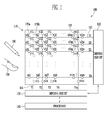
- FIG. 1 is a configuration block diagram of a touch screen system according to an exemplary embodiment of the present invention
- FIG. 2 is a conceptual circuit diagram of a touch screen panel shown in FIG. 1 ;
- FIG. 3A is a cross-sectional view of sensing cells under normal state (no touch) conditions
- FIG. 3B is a diagram schematically showing sensing results according to driving signals applied to each sensing cell shown in FIG. 3A ;
- FIG. 4A is a cross-sectional view of the sensing cells under a touched condition by a finger
- FIG. 4B is a diagram schematically showing the sensing results according to the driving signals applied to each sensing cell shown in FIG. 4A ;
- FIG. 5 is a block diagram showing a configuration of an active stylus according to an exemplary embodiment of the present invention.
- FIG. 6A is a cross-sectional view showing the sensing cells under an active stylus touched condition according to an exemplary embodiment of the present invention
- FIGS. 6B and 6C are diagrams schematically showing the sensing results according to the driving signals applied to each sensing cell shown in FIG. 6A ;
- FIG. 7 is a plan view showing an electrode pattern of a typical touch screen panel
- FIG. 8 is a graph for describing a problem when the active stylus moves, while touching the electrode pattern shown in FIG. 7 ;
- FIG. 9 is a plan view showing an electrode pattern of a touch screen panel according to an exemplary embodiment of the present invention.
- FIG. 10 is a graph for describing an effect when the active stylus moves, while touching the electrode pattern shown in FIG. 9 ;
- FIG. 11 is a plan view showing the electrode pattern of the touch screen panel according to another exemplary embodiment of the present invention.
- FIGS. 12A and 12B are plan views showing the electrode pattern of the touch screen panel according to yet another exemplary embodiment of the present invention.
- first element when a first element is described as being coupled to a second element, the first element may be directly coupled to the second element, or may be indirectly coupled to the second element via one or more third elements. Further, some of the elements that are not essential to the complete understanding of the invention are omitted for clarity. Also, like reference numerals refer to like elements throughout.
- FIG. 1 is a configuration block diagram of a touch screen system according to an exemplary embodiment of the present invention
- FIG. 2 is a conceptual circuit diagram of a touch screen panel shown in FIG. 1 .
- a touch screen system 100 is configured to include a touch screen panel 110 that includes a plurality of driving electrodes 170a (x11 to x1 m - xn1 to xnm). Each of the driving electrodes 170a is coupled to a corresponding one of a plurality of driving lines 112 (X1, X2,..., Xn) that extend in a first direction and a plurality of sensing electrodes 170b (y11 to y1 n to ym1 to xmn).
- Each of the sensing electrodes 170b is coupled to a corresponding one of a plurality of sensing lines 114 (Y1, Y2,...,Ym) that extend in a direction crossing the driving lines 112, and the sensing electrodes 170b and the plurality of driving electrodes 170a are alternately disposed so as not to overlap with each other.
- the touch screen system 100 also includes a driving circuit 120 for sequentially applying driving signals to each driving line 112, a sensing circuit 130 for detecting the change in capacitance sensed from each sensing line 114 in order to receive the generated sensing signals, a processor 140 for receiving the sensing signal from the sensing circuit 130 in order to determine the detected touch position, and an active stylus 160 to be used to touch the touch screen panel 110.
- the driving electrodes 170a and the sensing electrodes 170b may be formed on different layers or on the same layer.
- the driving electrodes 170a and the sensing electrodes 170b are alternately disposed to be close to each other without overlapping with each other.
- the driving electrodes 170a and the sensing electrodes 170b may be formed to be close to each other in a regular pattern like a diamond pattern.
- the shape of the electrodes is not limited to the diamond shape and may be implemented by various suitable shapes in which the driving electrodes and the sensing electrodes may be close to each other.
- the driving electrodes 170a and the sensing electrodes 170b are formed at the same layer, since a short would be generated at the crossing node 116 of the driving electrodes 170a and the sensing electrodes 170b, the driving electrodes 170a or the sensing electrodes 170b arranged at the same line are coupled to one another through a bridge pattern (not shown) formed at different layers, such that it prevents the occurrence of the short at the crossing region between the connection part of the sensing electrodes 170b and the connection part of the driving electrodes 170a.
- the active stylus 160 is configured to be separated from the touch screen panel 110.
- the active stylus 160 approaches or touches the touch screen panel 110, it is synchronized with the driving signals that are applied to the driving line 112 that is coupled to the adjacent driving electrode 170a, in order to generate an electric field.
- the plurality of driving electrodes 170a and sensing electrodes 170b may be made of a transparent conductive material, and the transparent conductive material may be made of indium tin oxide (ITO), indium zinc oxide (IZO), carbon nano tube (CNT), or the like.
- ITO indium tin oxide
- IZO indium zinc oxide
- CNT carbon nano tube
- a mutual capacitance is formed between adjacent driving electrodes 170a and sensing electrodes 170b that are alternately arranged with the driving electrodes 170a, and the mutual capacitance between each driving electrode 170a and a corresponding sensing electrode 170b functions as a sensing cell to perform touch recognition.
- the mutual capacitance, generated at the sensing cell generates the coupled sensing signals to the sensing line 114 that is coupled to the sensing electrode 170b included in the sensing cell, when the driving signals are applied to the driving line 112 that is coupled to the driving electrode 170a included in the sensing cell from the driving circuit 120.
- the mutual capacitance at each sensing cell is sensed through the sensing line that is coupled to each sensing cell when the driving signal is applied to the driving line that is coupled to each sensing cell.
- the driving circuit 120 sequentially applies the driving signals to each driving line X1, X2,...,Xn, and therefore, when the driving circuit 120 applies the driving signals to any one of the driving lines X1, X2,...,Xn, other driving lines remain in a ground state.
- the driving electrodes 170a coupled to the driving lines 112 that are applied with the driving signals, and the plurality of adjacent sensing electrodes 170b crossing the driving electrodes 170a, configure the sensing cells.
- the mutual capacitance is formed in each sensing cell. As described above, when the finger 150 or the stylus 160 touches the sensing cell, a corresponding change in capacitance occurs in the sensing cell.
- the touch screen panel 110 may be represented by the mutual capacitance.
- the touch screen panel 110 includes the driving electrode 170a that is coupled to the driving line 112 and the sensing electrode 170b that is coupled to the sensing line 114, wherein the driving electrode 170a and the sensing electrode 170b are spatially separated from each other to form a capacitance coupling node (e.g., the sensing cell 170).
- the driving line 112 is coupled to the driving circuit 120 that is represented as a voltage source
- the sensing line 114 is coupled to the sensing circuit 130.
- the driving electrode 170a and the sensing electrode 170b may each include a parasitic capacitance 170a' and 170b' (e.g., a predetermined parasitic capacitance).
- the driving electrode 170a and the adjacent sensing electrode 170b crossing therewith configure the sensing cell 170.
- the mutual capacitance of the sensing cell 170 is not changed, but when the conductive object approaches or touches the sensing cell 170, the mutual capacitance is changed.
- these changes cause a change in current (and/or voltage) to be transferred to the sensing line 114 that is coupled to the sensing cell 170.
- the sensing circuit 130 that is coupled to the sensing line 114 converts the information (sensing signal) on the change in capacitance and the position of the sensing cell 170 into a suitable type via, for example, an analog to digital converter, ADC, (not shown) and transfers the information to the processor 140 of FIG. 1 .
- ADC analog to digital converter
- the sensing circuit 130 senses the change in capacitance of the sensing line 114 that is coupled to the sensing cell 170
- the coordinates of the sensing line 114 in which the change in capacitance occurs and the coordinates of the sensing electrode 170a configuring the sensing cell 170, which is coupled to the driving line 112 that is applied with the driving signal from the driving circuit 120 are output, such that the coordinates of at least one sensing cell 170, in which the touch is made, are obtained.
- the driving circuit 120 scans (by sequentially applying the driving signals) the driving lines 112 and both continuously and concurrently (e.g., simultaneously) outputs the coordinates of the scanned driving lines to the sensing circuit 130, such that the sensing circuit 130 may obtain the position where the capacitance is changed, that is the position coordinates of the sensing electrode 170a configuring the sensing cell 170, while sensing the change in capacitance of the sensing line 114.
- the touch screen system can recognize a plurality of touched points, that is, the multi touch recognition.
- the above described exemplary embodiment of the present invention implements both the multi-touch recognition by the active stylus 160 and the multi-touch recognition by the person's finger 150.
- the multi-touch recognition may be implemented by the sharp active stylus that generates the electric field.
- the typical active stylus continuously generates and emits the electric field, therefore it is very difficult or impossible to accurately determine the touched position due to the influence of the continuously emitted electric field on the sensing cell corresponding to the actually touched position, as well as, to other sensing cells that are not touched.
- the active stylus when it approaches (or touches) a specific sensing cell, it amplifies and outputs the electric field in synchronization with the driving signal that is applied to the driving line coupled to the sensing cell, thereby making it possible to overcome the above described problem of the typical active stylus.
- the active stylus 160 when the active stylus 160, according to the exemplary embodiment of the present invention, touches the specific sensing cells 116 of the touch screen panel 110, the active stylus 160 generates the electric field to sense the touch only when the driving signal is applied to the sensing cells, such that the electric field has no effect on other sensing cells other than the touched sensing cells, thereby making it possible to implement the multi-touch recognition by the use of the active stylus.
- the exemplary embodiment of the present invention uses the fact that the change in mutual capacitance generated when the touch screen panel 110 is touched by the finger 150 and the change in mutual capacitance when the touch screen panel 110 is touched by the active stylus 160 are different from each other, to divide and process the changes accordingly in the sensing circuit 130 and the processor 140, thereby making it possible to implement various multi touch recognitions.
- FIG. 3A is a cross-sectional view of the sensing cell under the normal state (no touch) conditions
- FIG. 3B is a diagram schematically showing the sensing results according to the driving signals applied to each sensing cell shown in FIG. 3A .
- FIG. 3A shows the mutual capacitance electric field line 200 between the driving electrode 170a and the sensing electrode 170b that configure a single sensing cell 170 and are adjacently disposed at the same layer.
- a passivation layer 118 is formed on top of the driving electrode 170a and the sensing electrode 170b, but may be removed in some cases.
- the mutual capacitance (CM) is formed between the driving electrode 170a and the sensing electrode 170b that configure the sensing cell 170.
- the mutual capacitance CM generated at each sensing cell 170 is generated when the driving signal is applied to the driving line (112 of FIG. 1 ), which is coupled to the driving electrode 170a configuring each sensing cell, from the driving circuit 120.
- the driving circuit 120 is integrated together with the above-mentioned sensing circuit 130 and the processor 140, such that they may be included in a single IC chip.
- the driving circuit 120 sequentially applies the driving signals (for example, a voltage of 3V) to each driving line X1, X2,...,Xn, and therefore, when the driving circuit 120 applies the driving signals to any one of the driving lines X1, X2,...,Xn, other driving lines remain in a ground state (e.g., 0V).
- FIG. 3B shows an example where the driving signal is applied to the first driving line X1.
- FIG. 3B shows the case where the driving electrode 170a and the adjacent sensing electrode 170b configure each sensing cell 170 (S11 to Snm).
- the plurality of driving electrodes 170a (x11 to x1 m to xn1 to xnm), which are coupled to the plurality of driving lines 112, and the plurality of sensing electrodes 170b (y11 to y1 n to ym1 to ymn), which are coupled to the plurality of sensing lines 114 that extend in a direction crossing the driving lines 112, are alternately disposed so as not to overlap with each other.
- the sensing cell S11 is configured to include the driving electrode x11 and the sensing electrode y11 adjacent thereto
- the sensing cell Snm is configured to include the driving electrode xnm and the sensing electrode ymn adjacent thereto.
- the mutual capacitance between each driving electrode and each sensing electrode configuring the plurality of sensing cells S11, S12,..,S1m is formed in the plurality of sensing cells S11, S12,...,S1m, such that the voltage (for example, 0.3V) corresponding to the mutual capacitance is sensed by the sensing lines Y1, Y2,.., Ym coupled to each sensing cell applied with the driving signal.
- FIG. 4A is a cross-sectional view of the sensing cell under the touched conditions by a finger
- FIG. 4B is a diagram schematically showing the sensing results according to the driving signals applied to the each sensing cell shown in FIG. 4A .
- the electric field line 210 between the driving electrode 170a and the sensing electrode 170b is interrupted as shown, and the electric field line is branched into the finger 150 and a ground through the capacitance path of the body of the person, such that the mutual capacitance CM1 at the sensing cell 170 is smaller than the mutual capacitance CM at the normal state shown in FIG. 3A (CM1 ⁇ CM).
- the change in mutual capacitance at each sensing cell 170 changes the voltage transferred to the sensing line 114 that is coupled to the sensing cell 170.
- each mutual capacitance CM is formed at each sensing cell S11, S12,...,S1m configured to include the plurality of sensing electrodes 170b adjacently crossing the plurality of driving electrodes 170a.
- the first driving line X1 that is coupled to the driving electrodes 170a is applied with the driving signal (for example, a voltage of 3V), which is sequentially applied to the driving lines X1, X2,...,Xn by the driving circuit (e.g., 120 of FIG. 1 ).
- the mutual capacitance CM1 is reduced, and thus the voltage (for example, 0.1V) corresponding to the reduced mutual capacitance is sensed by the sensing lines Y2 and Ym that are coupled to the touched sensing cells S12 and S1 m, respectively.
- sensing cells which are coupled to the first driving line X1 but are not touched by the finger 150, maintain their existing mutual capacitance CM unchanged, such that the above-mentioned voltage (for example, 0.3V) is sensed by the sensing lines that are coupled to the sensing cells.
- the above-mentioned voltage for example, 0.3V
- the sensing circuit e.g., the sensing circuit 130 of FIG. 1
- the sensing circuit 130 of FIG. 1 converts the information (sensing signal) on the change and position of the touched sensing cells S12 and S1 m into a suitable type via an ADC (not shown) and transfers the information to the processor (e.g., the processor 140 of FIG. 1 ).
- a touched area (A) is about 6mm per side.
- the touched area is generally larger than that of the driving electrode 170a and the sensing electrode 170b that configure the sensing cell 170. Therefore, when using the finger 150, it is difficult to implement more precise touch recognition.
- the touched surface is small, and thus, the change in capacitance at the touched surface is very slight, such that it is difficult to perform the detection.
- the above described exemplary embodiment of the present invention can implement the multi-touch recognition using the sharp active stylus together with the multi-touch recognition using the finger, thereby overcoming the problem in the related art.
- the typical active stylus has a configuration that continuously generates and emits the electric field, such that it is impossible or very difficult to accurately determine the touched position due to the influence of continuously emitted electric field on the sensing cell corresponding to the actually touched position, as well as, to other sensing cells that are not touched.
- the active stylus when it approaches (or touches) the specific sensing cell, it has a configuration that amplifies/outputs the electric field in synchronization with the driving signal that is applied to the driving line coupled to the sensing cell.
- FIG. 5 is a block diagram showing a configuration of an active stylus according to an exemplary embodiment of the present invention.
- FIG. 5 is a block diagram that conceptually illustrates each component of the active stylus and does not show the appearance of the active stylus.
- the active stylus may be implemented as a conductor having a shape in which an area of a portion for contacting the touch screen panel is small (e.g., smaller than a finger).
- the active stylus 160 is configured to include an electric field sensing sensor 162 that senses an electric field generated by the driving signal applied to the driving electrode 170a that is touched (or approached) by the active stylus 160; a signal generator 164 that generates a signal (e.g., a predetermined signal such as an AC voltage) for generating a separate electric field corresponding to the sensed electric field; an electric field emitter 166 that amplifies the signal generated from the signal generator 164 and outputs the amplified signal as an electric field; and a power supply 168 that supplies power to each of the components 162, 164, and 166.
- a signal e.g., a predetermined signal such as an AC voltage
- the electric field sensing sensor 162 may be implemented to include a coil so as to sense the electric field generated by applying the driving signal. That is, the electric field sensing sensor 162 is positioned in the electric field forming region that is generated by the driving signal, such that an electric force may be sensed by the electric field sensing sensor 162.
- the signal generator 164 when the electric field is sensed by the electric field sensing sensor 162, the signal generator 164 generates the predetermined signal accordingly. For example, an AC voltage having the same phase as the driving signal may be generated corresponding to the sensed electric field.
- the signal (e.g., an AC voltage) generated through the signal generator 164 is amplified through the electric field emitter 166, and the amplified signal is output as an electric field through the end of the stylus 160.
- the electric field emitter 166 may be implemented to include a non-inverting amplifier that amplifies the amplitude of the AC voltage while maintaining the phase of the generated AC voltage as it is and an inverting applifier that inverts the amplitude of the AC voltage while maintaining the phase of the AC voltage.
- the active stylus 160 touches specific sensing cells 170 of the touch screen panel 110, it senses the touch only when the driving signal is applied to the sensing cells to generate the electric field. Therefore, the electric field has no effect on other sensing cells other than the touched sensing cells, that is, the other sensing cells that are coupled to the driving lines are in the ground state, thereby making it possible to implement the multi-touch recognition by the use of the active stylus.
- FIG. 6A is a cross-sectional view of the sensing cell under the active stylus touched conditions according to an exemplary embodiment of the present invention
- FIGS. 6B and 6C are diagrams schematically showing the sensing results according to the driving signal applied to each sensing cell shown in FIG. 6A .
- FIG. 6A shows an example in which the electric field that is output by the active stylus 160 is amplified by the non-inverting amplifier.
- the state in which the sensing cell 170 is touched is substantially the same as the embodiment described in FIGS. 3A and 3B , and the description thereof will be omitted.
- FIG. 6A it illustrates the change in mutual capacitance at the sensing cell 170 due to the touch of the active stylus 160 in the state in which the driving signal is applied to the driving line 112.
- the active stylus 160 touches at least one sensing cell 170, the active stylus 160 senses the electric field that is generated by the driving signal applied to the driving electrode 170a of the sensing cell 170, and amplifies/outputs the corresponding electric field.
- the electric field sensing sensor 162 senses the electric field that is generated by the driving signal, and the electric field emitter 166, as an emitter Em, amplifies/outputs the corresponding electric field.
- the first electric field line 220 of FIG. 6A illustrates an electric field generated by the application of the driving signal
- the second electric field line 600 illustrates the electric field output from the active stylus 160.
- the electric field output from the active stylus 160 corresponds to the AC voltage output through the non-inverting amplifier, wherein the AC voltage has the same phase as the driving signal corresponding to the electric field generated by the application of the driving signal.
- the first and second electric field lines (220 and 600) are each formed in a direction toward the sensing electrode 170b from the driving electrode 170a or the active stylus 160.
- the mutual capacitance CM2 between the driving electrode 170a and the sensing electrode 170b is increased as compared to the mutual capacitance CM at a normal state (non-touched state) (CM2 > CM).
- the change in mutual capacitance at each sensing cell changes the voltage transferred to the sensing electrode 170b that is coupled to the sensing cell 170.
- the driving circuit (120 of FIG. 1 ) sequentially applies the driving signals (for example, a voltage of 3V) to each driving line X1, X2,...,Xn, and therefore, when the driving circuit 120 applies the driving signals to any one of the driving lines X1, X2,...,Xn, other driving lines remain in a ground state.
- FIG. 6B shows an example where the driving signal is applied to the first driving line X1.
- a mutual capacitance CM is formed in each of the plurality of sensing cells S11, S12,...,S1m configured to include the plurality of sensing electrodes 170b adjacently crossing the plurality of driving electrodes 170a that are coupled to the first driving line X1 applied with the driving signal.
- the mutual capacitance CM2 is increased, such that a voltage (for example, 0.5V) corresponding to the increased mutual capacitance is sensed by the sensing lines Y1 and Y2 that are coupled to the touched sensing cells S11 and S12.
- sensing cells which are coupled with the first driving line X1 but are not touched by the active stylus 160, maintain their existing mutual capacitances CM as they are, such that a different voltage (for example, 0.3V) is sensed by the sensing lines that are coupled to the sensing cells.
- a different voltage for example, 0.3V
- the active stylus 160 does not sense the electric field since the driving signal is not applied to the driving line X1 that is coupled to the touched sensing cells S11 and S12, such that the active stylus 160 does not output a separate electric field.
- the active stylus 160 is a passive conductor, such that the touch recognition may not be performed. That is, the voltage (for example, 0.3V) corresponding to all the existing mutual capacitances CM is sensed by the sensing lines Y1, Y2,...,Ym.
- the stylus 160 may erronously sense touching with the sensing cells S21 and S22 even though the stylus does not actually touch the sensing cells S21 and S22.
- the active stylus 160 touches the specific sensing cells 170 of the touch screen panel 110, it senses touching only when the driving signal is applied to the sensing cells in order to generate the electric field, such that the electric field has no effect on other sensing cells other than the touched sensing cells. That is, other sensing cells are coupled to the driving lines that are in the ground state, thereby making it possible to implement the multi-touch recognition by the use of the active stylus.
- the sensing circuit 130 that is coupled to the sensing lines Y1, Y2,...,Ym converts the information (sensing signal) on the change in capacitance and position of the touched sensing cells S12 and S1 m into a suitable type via the ADC (not shown) and transfers the information to the processor 140.
- the above described exemplary embodiment of the present invention uses the fact that the change in mutual capacitance generated when the finger 150 touches the sensing cell and the change in mutual capacitance when the active stylus 160 touches the sensing cell are different from each other, to recognize and process the changes in the sensing circuit 130 and the processor 140, thereby making it possible to implement various multi-touch recognitions.
- the touches may be differentiated and recognized.
- the amplitude (for example, 0.5V) of the sensing signal that is sensed by the sensing line has a large difference from the amplitude (for example, 0.2V) of the sensing signal that is generated by the touch of the finger, which may be easily differentiated by, for example, an amplitude detector (not shown) and/or an amplitude comparator (not shown) that are included in the sensing circuit 130.
- the driving electrode 170a and the sensing electrode 170b configuring the sensing cell 170 have the same area and pattern, and when the active stylus 160, not the finger 150, moves while touching the sensing cell 170, it is difficult to accurately sense the touched position since there is no position correlation between the moving stylus 160 and the sensing cell 170 corresponding thereto.
- FIG. 7 is a plan view showing an electrode pattern of a typical touch screen panel
- FIG. 8 is a graph for describing the case where the active stylus moves while touching the electrode pattern shown in FIG. 7 .
- the sensing cells 170 are each configured to include the driving electrodes 170a and the sensing electrodes 170b adjacently crossing therewith.
- the plurality of driving electrodes 170a are coupled to one another along a first direction (e.g., X-axis direction), and the sensing electrodes 170b and the driving electrodes 170a are alternately disposed so as not to overlap with each other.
- the sensing electrodes 170b are coupled to each other along a second direction (e.g., Y-axis direction) that crosses the first direction.
- the driving electrodes 170a and the sensing electrodes 170b are configured in the same diamond shape and have substantially the same area.
- driving electrodes 170a and the sensing electrodes 170b are each coupled in a line unit along the first and second directions, respectively, by first and second connection patterns 170a1 and 170b1, respectively, as shown.
- the first and/or second connection patterns 170a1 and 170b1 may be each patterned as an independent pattern to be coupled to the driving electrode or the sensing electrode 170a and 170b by an indirect connection, or may be patterned to be integrally coupled to the driving electrode or the sensing electrode 170a and 170b from a same step of patterning the driving electrode or the sensing electrode 170a and 170b.
- the first connection patterns 170a1 are each patterned to be an independent pattern at the upper or lower portion of the driving electrodes 170a, such that the driving electrodes 170a may be coupled in a line unit along the first direction while being electrically connected to one another by the first connection patterns 170a1 at the upper portion or the lower portion of the driving electrodes 170a.
- the first connection patterns 170a1 may be formed using a transparent electrode material such as ITO, etc., that is similar to the electrodes 170a and 170b or may be formed using an opaque low resistance material, but may be formed controlling its width, etc., so as to prevent the visualization of the patterns.
- a transparent electrode material such as ITO, etc.
- connection patterns 170b1 may be integrally patterned with the sensing electrodes 170b in a step of patterning the electrodes 170a and 170b in order to couple the sensing electrodes 170b in a line unit along the second direction.
- an insulating layer (not shown) is interposed between the first connection patterns 170a1 and the second connection patterns 170b1 in order to secure their stability. Through this, even though the driving electrodes 170a and the sensing electrodes 170b are formed on the same layer, the short circuit at the crossing point of the electrodes may be prevented.
- the driving signal is applied to the driving line (112 of FIG. 1 ) that is coupled to the driving electrode 170a and the sensing signal corresponding thereto is applied to the sensing circuit (130 of FIG. 1 ) through the sensing line (114 of FIG. 1 ) that is coupled to the sensing electrode 170b.
- the driving electrode 170a and the sensing electrode 170b configuring the sensing cell 170 have the same area and pattern, when the active stylus 160, according to the exemplary embodiment of the present invention described with reference to FIGS. 5 and 6 , moves while touching the sensing cell 170, it may be difficult to accurately sense the touched position regardless of the position correlation between the moving active stylus 160 and the sensing cell 170 corresponding thereto.
- the description will be made under the assumption that the active stylus 160 moves in the arrow direction shown in FIG. 7 .
- the active stylus 160 which is approaching or touching point A of FIG. 7 , moves from the left end to the right end via the center of the electrode 170a. That is, the active stylus 160 moves through a path (P) between the left and right corners of the driving electrode 170a of the sensing cell 170.
- the sensing signal is represented by a product of a driving signal Tx_RC sensed by the electric field sensing sensor 162, an amplification gain of an amplifier included in the electric field emitter 166, and a signal Em_Rx that is an output from the electric field emitter and is applied to the sensing electrode 170b.
- the sensing signal is equal to Tx_RC * (amplification gain) * Em_Rx, and the active stylus 160 through the sensing signal estimates the adjacent or touched position, such that the sensing signal and the position of the active stylus 160 should have the function relationship of 1 : 1.
- the strength of the driving signal Tx_RC sensed at the central portion of the driving electrode 170a becomes the largest when the active stylus moves in the arrow direction from point A of FIG. 7 , that is, when the active stylus moves from the left end of the driving electrode 170a of the sensing cell 170 to the right end via the center.
- the shape of the driving electrode 170a is a diamond shape, when the active stylus 160 is positioned at the center of the driving electrode, the overlapping area of the active stylus 160 and the driving electrode becomes the largest, as compared to the case where the active stylus 160 is positioned in other regions.
- the position for sensing the most of the electric field lines generated from the driving electrode 170a becomes the central portion of the driving electrode, and the overlapping area of the active stylus 160 and the driving electrode is reduced or minimized at the left and right ends of the driving electrode, such that the strength of the driving signal Tx_RC sensed by the electric field sensing sensor 162 of the active stylus 160 is the smallest in the region near the ends.
- the strength of the signal Em_Rx that is output from the electric emitter 166 of the active stylus and applied to the sensing electrode 170b, is gradually reduced as the area overlapping with the sensing electrode 170b is gradually reduced as shown in FIG. 7 , when the active stylus moves in the arrow direction from point A of FIG. 7 , that is, when the active stylus moves from the left end of the driving electrode 170a configuring the sensing cell 170 to the right end via the center.
- the final sensing signal becomes a signal shown in FIG. 8(c) corresponding to a product of the signal Tx_RC shown in FIG. 8(a) and the signal Em_RX shown in FIG. 8(b) .
- the sensing signal shown in FIG. 8C does not have the function relationship with the position of the active stylus 160 as shown.
- the active stylus 160 when the active stylus 160, according to the exemplary embodiment of the present invention, is applied to the touch screen panel having the electrode pattern of FIG. 7 , it is difficult to accurately recognize the position of the active stylus 160.
- an exemplary embodiment of the present invention improves or optimizes the electrode pattern structure of the touch screen panel, thereby making it possible to improve the accuracy of the multi-touch recognition implementation by the active stylus.
- the electrode pattern structure of the touch screen panel according to an exemplary embodiment of the present invention will be described with reference to FIGS. 9 to 11 .
- FIG. 9 is a plan view showing the electrode pattern of the touch screen panel according to an exemplary embodiment of the present invention
- FIG. 10 is a graph for describing the case when the active stylus moves, while touching the electrode pattern shown in FIG. 9 .
- sensing cells 270 are each configured to include the driving electrodes 270a and the sensing electrodes 270b that are adjacent to and alternately arranged with the driving electrodes 270a.
- the plurality of driving electrodes 270a are coupled to one another along the first direction (X-axis direction), and the sensing electrodes 270b are alternately disposed with the driving electrodes 270a so as not to overlap with each other, but the sensing electrodes 270b are coupled to each other along a second direction (Y-axis direction) that crosses the first direction.
- the driving electrodes 270a and the sensing electrodes 270b are each coupled in a line unit along the first and second directions by first and second connection patterns 270a1 and 270b1, respectively, which are shown in the enlarged region of FIG. 9 as the crossing point.
- first and/or second connection patterns 270a1 and 270b1 may be each patterned to have an independent pattern to be coupled to the driving electrode 270a or the sensing electrode 270b by a direct or an indirect connection, or may be patterned to be integrally coupled to the driving electrode 270a or the sensing electrode 270b in a step of patterning the driving electrode 270a or the sensing electrode 270b.
- the first connection patterns 270a1 are each patterned on the upper or lower layer of the driving electrodes 270a as the independent pattern, such that the driving electrodes 270a may be coupled in a line unit along the first direction while being electrically coupled to one another by the first connection patterns 270a1 at the upper portion or the lower portion of the driving electrodes 270a.
- the first connection patterns 270a1 may be formed using the transparent electrode material such as ITO, etc., that is similar to the electrodes 270a and 170b, or may be formed using the opaque low resistance material, but may be formed while controlling its width, etc., so as to prevent the visualization of the pattern.
- connection patterns 270b1 may be integrally patterned with the sensing electrodes 270b, in a step of patterning the electrodes 270a and 270b, to couple the sensing electrodes 270b to one another in a line unit along the second direction.
- an insulating layer (not shown) may be interposed between the first connection patterns 270a1 and the second connection patterns 270b1 in order to secure their stability.
- the exemplary embodiment of the present invention is configured in a different type such that the driving electrodes 270a and the sensing electrodes 270b have different areas.
- the length of the driving electrodes 270a in the second direction that is the vertical height thereof, is implemented to be shorter than the length of the sensing electrodes 270b in the second direction.
- the driving electrodes 270a are implemented in a polygon shape of which the length in the first direction (left to right width P) is longer than the length in the second direction (vertical height H). That is, when comparing with the driving electrode pattern shown in FIG. 7 , the driving electrode pattern is relatively flat or elongated in the second direction and has a shape more extended in the left and right directions.
- the sensing electrodes 270b are implemented in a shape including a body 271 b extending in a height or vertical direction (the second direction, Y-axis direction) and a plurality of protrusions 272b1 and 272b2 protruded from the left and right of the body 271b, respectively, that is, in the first direction (X-axis direction).
- the first protrusions 271 b1 protruded at the left of the body 271 b and the second protrusions 271 b2 protruded at the right thereof are arranged in an X-shape or offset. Therefore, in the adjacent sensing electrodes 270b, the second protrusions 271 b2 of a left sensing electrode and the first protrusions 271 b1 of a right sensing electrode are arranged in an X-shape or interleaved, as shown in FIG. 9 .
- the driving signal is applied to the driving line (112 of FIG. 1 ) that is coupled to the driving electrode 270a, and the sensing signal corresponding to driving signal is applied to the sensing circuit (130 of FIG. 1 ) through the sensing line (114 of FIG. 1 ) that is coupled to the sensing electrode 270b.
- the exemplary embodiment of FIG. 9 configures the driving electrode 270a and the sensing electrode 270b of the sensing cell 270 in different shapes, such that when the active stylus 160, according to the exemplary embodiment of the present invention described with reference to FIGS. 5 and 6 , moves while touching the sensing cell 270, the accuracy of the touch recognition may be implemented by the active stylus 160, by maintaining the position correlation between the moving active stylus 160 and the sensing cell 270 corresponding thereto.
- the strength of the driving signal Tx_RC that is sensed by the electric field sensing sensor 162 of the active stylus 160 becomes substantially constant when the active stylus moves in the arrow direction from point B of FIG. 9 , that is, when the active stylus moves from the left end of the driving electrode 270a of the sensing cell 270 to the right end via the center.
- the driving electrode 270a With the shape of the driving electrode 270a as shown in FIG. 9 , the height of the central portion of the driving electrode 270a is considerably reduced to have a shape more extended in the left and right directions. Therefore, the driving electrode 270a has a more flat or elongated shape when it is compared with the driving electrode 170a shown in FIG. 7 .
- the driving electrode 170a having the diamond shape shown in FIG. 7 when the active stylus 160 is disposed at the center of the driving electrode 170a, the overlapping area between the active stylus 160 and the driving electrode 170a is considerably large, as compared with the case where the active stylus 160 is positioned in other regions, such that the active stylus 160 at the center position of the driving electrode 170a senses the most amount of electric field lines that are generated by the driving electrode 170a as compared with other regions.
- the driving electrode 270a having the shape shown in FIG. 9 the height H of the central portion of the driving electrode 270a is considerably reduced as compared with the driving electrode 170a.
- the strength of the signal Em_Rx that is output from the electric emitter 166 of the active stylus and applied to the sensing electrode 270b, is gradually reduced as the area overlapping with the sensing electrode 270b is gradually reduced as shown in FIG. 9 , when the active stylus 160 moves in an arrow direction from point B of FIG. 9 , that is, when the active stylus moves from the left end of the driving electrode 270a of the sensing cell 270 to the right end via the center.
- the sensing electrode 270b shown in FIG. 9 includes the plurality of protrusions 272b1 and 272b2 protruded in the left and right directions of the body 271 b that extends in the height direction (second direction, Y-axis direction), such that the area overlapping with the sensing electrode 270b is large as compared with the exemplary embodiment shown in FIG. 7 , even though the active stylus moves.
- the strength of the Em-Rx signal is relatively larger than that of the Em_Rx signal shown in FIG. 8(b) .
- the final sensing signal becomes a signal shown in FIG. 10(c) corresponding to a product of the signal Tx_RC shown in FIG. 10(b) and the signal Em_RX shown in FIG. 10(b) .
- the Tx_RC shown in FIG. 10(a) has a function relation of 1 : 1, that is, a linear characteristic, and the strength of signal Em_Rx shown in FIG. 10(b) is relatively large, such that the sensing signal shown in FIG. 10(c) has the function relationship with the position of the active stylus 160 and the strength of the absolute signal is large.
- FIG. 11 is a plan view showing the electrode pattern of the touch screen panel according to an exemplary embodiment of the present invention.
- the electrode pattern shown in FIG. 11 is similar to the electrode pattern structure shown in FIG. 9 , and therefore, like components are denoted by like reference numerals. As a result, the description thereof will not be described for convenience.
- the driving electrodes 270a are implemented in a shape including the body 271 a extending in a longitudinal direction (the first direction, X-axis direction) and the protrusions 272a1 and 272a2 protruded from the upper and lower portions of the body 271a, respectively, in the second direction (Y-axis direction).
- the body 271 a has substantially the same shape as the driving electrode 270a shown in FIG. 9 and is implemented in a polygon shape of which the length of the first direction (left to right width P) is longer than the length of the second direction (vertical height H).
- the sensing electrodes 270b have the same shape as the sensing electrodes 270b shown in FIG. 9 and are implemented in a shape including a body 271 b arranged in a height direction (second direction, Y-axis direction) and a plurality of protrusions 272b1 and 272b2 protruded from the left and right of the body 271b, that is, the first direction (X-axis direction).
- the first protrusions 271b1 protruded at the left of the body 271b and the second protrusions 271 b2 protruded at the right thereof are arranged in an X-shape or offset. Therefore, in the adjacent sensing electrodes 270b, the second protrusions 271 b2 of the left sensing electrodes and the first protrusions 271 b1 of the right sensing electrodes are arranged in an X-shape or interleaved, as shown.
- the first protrusion 271 a1 protruded from the upper side and the second protrusion 271 a2 protruded from the lower side of the body 271 a of the driving electrode are implemented in a zigzag shape disposed between the first and second protrusions 271 b1 and 271 b2 of the adjacent sensing electrodes 270b.
- the entire area of the driving electrode 270a may be implemented wider, such that the touch recognition sensitivity of the active stylus 160 may be more improved.
- FIGS. 12A and 12B are plan views showing the electrode pattern of the touch screen panel according to another exemplary embodiment of the present invention.
- the electrode pattern structure according to the exemplary embodiment shown in FIGS. 12A and 12B is also implemented to maintain the position correlation between the active stylus 160 and the sensing cells 370 and 370' corresponding thereto.
- the sensing cell 370 is configured to include a driving electrode 370a that is coupled to the driving line 112 and a sensing electrode 370b that is coupled to the sensing line 114 while being adjacent to the driving electrode 370a. That is, a region represented by a dotted line in FIG. 12A corresponds to the sensing cell 370.
- the driving electrode 370a and the sensing electrode 370b are each implemented as a combination of a plurality of fine patterns 370as and 370bs, respectively, as shown in FIG. 12A .
- the plurality of fine patterns 370as of the driving electrode 370a may be arranged in, for example, a 5x5 matrix type as shown, and the plurality of second fine patterns 370bs of the sensing electrode 370b corresponding thereto may be arranged in the 5x5 matrix type such that they are alternately disposed with the first fine patterns 370as without overlapping with each other.
- first fine patterns 370as and the second fine patterns 370bs adjacent thereto may be implemented to have the same structure as the arrangement and connection of the electrode patterns shown in FIG. 7 , and therefore, the detailed description thereof will be omitted.
- the fine touch by the stylus may be sensed by implementing the driving electrode 370a and the sensing electrode 370b in the plurality of fine patterns 370as and 370bs.
- the electrode pattern structure may be changed as shown in FIG. 12B .
- a driving electrode 370a' configuring a sensing cell 370' includes only a single line of first fine patterns 370as'.
- the same effect as using the driving electrode shown in FIGS. 9 and 11 may be obtained by reducing the length of the height direction of the driving electrode 370as'.
- the region of other first fine patterns may be provided with an island dummy pattern 370c or third fine patterns 370bs" that are coupled to the second fine patterns 370bs' of the sensing electrode 370b', as shown in FIG. 12B .
- FIGS. 7 to 11 show an example where the active stylus 160 moves in the specific region, but the exemplary embodiment of the present invention is not limited thereto.
- the active stylus 160 may be applied to all the regions of the touch screen panel that is approached or touched by the active stylus 160.
- the position correlation between the active stylus 160 and the sensing cell (170, 270 or 370) corresponding thereto may be maintained, such that the accuracy of the touch recognition implementation by the active stylus may be improved.
- the electrode pattern structure according to the present invention is not limited to the exemplary embodiment shown in FIGS. 9 , 11 , and 12 . While the present invention has been described in connection with certain exemplary embodiments, it is to be understood that the invention is not limited to the disclosed embodiments, but, on the contrary, is intended to cover various modifications and equivalent arrangements included within the scope of the appended claims, and equivalents thereof.
Abstract
Description
- Aspects of embodiments according to the present invention relate to a touch screen system.
- A touch screen panel is an input device that selects instructions displayed on a screen, such as an image display device, etc., by using a person's hand or an object to input instructions of a user.
- To this end, the touch screen panel is provided on a front face of the image display device and converts positions that are directly touched by a person's hand or an object into electrical signals. Therefore, the instructions selected at the touched positions are received as the input signals. As the touch screen panel can replace a separate input device, such as a keyboard or a mouse, that is operated by being connected to the image display device, the application field of the touch screen panel is being gradually expanded.
- Types of the touch screen panel include a resistive type, a light sensing type, a capacitive type, etc.
- Recently, there has been increased interest in a multi-touch screen system capable of performing multi-touch recognition through the touch screen panel. In particular, in the case of the capacitive type, the multi-touch recognition may be implemented as a self capacitance type or a mutual capacitance type. When at least one finger of a person touches the surface of the touch screen panel, the capacitive type touch screen panel detects a change in capacitance formed in sensing cells that are positioned at the touched surface to recognize the touched positions.
- However, according to these schemes, it is difficult to recognize more precise touch positions through the touch by a person's finger.
- In order to overcome the above-mentioned problems, a sharp stylus may be used. In the case of a passive stylus, the change in capacitance is very slight at the touched surface, such that it is difficult to detect the touched position. On the other hand, an active stylus can generate an electric field. The generated electric field has an effect on the sensing cells of the touch screen panel corresponding to the actually touched position and other sensing cells coupled to a sensing line that is affected by the generated electric field, such that it may be impossible or difficult to determine the touched positions.
- Therefore, aspects of embodiments according to the present invention are directed toward a touch screen system capable of implementing both multi-touch recognition by a person's finger and multi-touch recognition by an active stylus, wherein the touch screen system is a mutual capacitance type.
- It is another aspect of the embodiments according to the present invention to provide a touch screen system that includes an optimized structure of an electrode pattern capable of improving the accuracy of touch recognition by an active stylus.
- A touch screen system according to an exemplary embodiment of the present invention includes: a touch screen panel including a plurality of driving electrodes coupled to a plurality of driving lines extending in a first direction and a plurality of sensing electrodes coupled to a plurality of sensing lines extending in a second direction crossing the first direction, the driving electrodes and the sensing electrodes being alternately arranged so as not to overlap with each other; and an active stylus separated from the touch screen panel, the active stylus being configured to output an electric field in synchronization with driving signals that are applied to the driving lines coupled to the driving electrodes adjacent to the active stylus, wherein the driving electrodes and the sensing electrodes have different areas.
- One of the driving electrodes may have a polygon shape having a length in the first direction longer than a length in the second direction, and the length in the second direction of one of the driving electrodes may be shorter than a length in the second direction of one of the sensing electrodes.
- The sensing electrodes may have a shape including a body extending in the second direction and a plurality of protrusions protruded in the first direction from the left and right of the body.
- The protrusions may include first protrusions protruded from the left of the sensing electrode body and second protrusions protruded from the right of the sensing electrode body, and the first protrusions and the second protrusions may be arranged to be offset in the second direction, and the first protrusions of one of the sensing electrodes and the second protrusion of an adjacent one of the sensing electrodes may be arranged to be offset in the second direction.
- One of the driving electrodes may have a shape including a body extending in the first direction and at least one protrusion that protrudes in the second direction from upper or lower portions of the body, and the body of the driving electrode may have a polygon shape having a length in the first direction longer than a length in the second direction.
- The at least one protrusion protruded from the body of the driving electrode may be between adjacent ones of the sensing electrodes.
- The plurality of driving electrodes are coupled to each other along the first direction, and the plurality of sensing electrodes are coupled to each other along the second direction.
- The plurality of driving electrodes and sensing electrodes may be located at the same layer and may include a transparent conductive material.
- The driving electrodes and the sensing electrodes may include a plurality of fine patterns.
- Adjacent ones of the driving electrodes and the sensing electrodes may configure independent sensing cells.
- The touch screen system may further include: a driving circuit for sequentially applying driving signals to the driving lines; a sensing circuit coupled to the sensing lines, the sensing circuit being configured to receive sensing signals generated by detecting a change in capacitance from each of the sensing cells; and a processor for receiving the sensing signals from the sensing circuit to determine touched positions.
- The active stylus may include: an electric field sensing sensor for sensing a first electric field generated by the driving signals that are applied to one of the driving lines that is touched or approached by the active stylus; a signal generator for generating a signal in order to generate a second electric field corresponding to the sensed first electric field; an electric field emitter for amplifying the signal generated from the signal generator and outputting the amplified signals as the second electric field; and a power supply for applying power to the electric field sensing sensor, the signal generator, and the electric field emitter.
- The signal generated from the signal generator may be an AC voltage having a same phase as the driving signals.
- The electric emitter may include a non-inverting amplifier that maintains a phase of a signal (e.g., a predetermined signal) generated from the signal generator and may amplify the amplitude of the signal generated from the signal generator.
- As set forth above, the exemplary embodiments of the present invention implement the multi-touch recognition by the person's finger using the touch screen panel of the mutual capacitance scheme and the multi-touch recognition by the active stylus. The change in mutual capacitance generated when the finger is touched and the change in mutual capacitance generated when the active stylus is touched are different from each other, and the changes are differentiated and processed, thereby making it possible to perform various and more precise multi-touch recognition.
- Further, the exemplary embodiments of the present invention optimize the electrode pattern structure of the touch screen panel, thereby making it possible to improve the accuracy of the multi-touch recognition implementation by the active stylus.
- The accompanying drawings, together with the specification, illustrate exemplary embodiments of the present invention, and, together with the description, serve to explain the principles of the present invention.
-
FIG. 1 is a configuration block diagram of a touch screen system according to an exemplary embodiment of the present invention; -
FIG. 2 is a conceptual circuit diagram of a touch screen panel shown inFIG. 1 ; -
FIG. 3A is a cross-sectional view of sensing cells under normal state (no touch) conditions; -
FIG. 3B is a diagram schematically showing sensing results according to driving signals applied to each sensing cell shown inFIG. 3A ; -
FIG. 4A is a cross-sectional view of the sensing cells under a touched condition by a finger; -
FIG. 4B is a diagram schematically showing the sensing results according to the driving signals applied to each sensing cell shown inFIG. 4A ; -
FIG. 5 is a block diagram showing a configuration of an active stylus according to an exemplary embodiment of the present invention; -
FIG. 6A is a cross-sectional view showing the sensing cells under an active stylus touched condition according to an exemplary embodiment of the present invention; -
FIGS. 6B and 6C are diagrams schematically showing the sensing results according to the driving signals applied to each sensing cell shown inFIG. 6A ; -
FIG. 7 is a plan view showing an electrode pattern of a typical touch screen panel; -
FIG. 8 is a graph for describing a problem when the active stylus moves, while touching the electrode pattern shown inFIG. 7 ; -
FIG. 9 is a plan view showing an electrode pattern of a touch screen panel according to an exemplary embodiment of the present invention; -
FIG. 10 is a graph for describing an effect when the active stylus moves, while touching the electrode pattern shown inFIG. 9 ; -
FIG. 11 is a plan view showing the electrode pattern of the touch screen panel according to another exemplary embodiment of the present invention; and -
FIGS. 12A and12B are plan views showing the electrode pattern of the touch screen panel according to yet another exemplary embodiment of the present invention. - Hereinafter, certain exemplary embodiments according to the present invention will be described with reference to the accompanying drawings. Here, when a first element is described as being coupled to a second element, the first element may be directly coupled to the second element, or may be indirectly coupled to the second element via one or more third elements. Further, some of the elements that are not essential to the complete understanding of the invention are omitted for clarity. Also, like reference numerals refer to like elements throughout.
- Hereinafter, exemplary embodiments of the present invention will be described in more detail with reference to the accompanying drawings.
-
FIG. 1 is a configuration block diagram of a touch screen system according to an exemplary embodiment of the present invention, andFIG. 2 is a conceptual circuit diagram of a touch screen panel shown inFIG. 1 . - A
touch screen system 100 according to an exemplary embodiment of the present invention is configured to include atouch screen panel 110 that includes a plurality of drivingelectrodes 170a (x11 to x1 m - xn1 to xnm). Each of the drivingelectrodes 170a is coupled to a corresponding one of a plurality of driving lines 112 (X1, X2,..., Xn) that extend in a first direction and a plurality ofsensing electrodes 170b (y11 to y1 n to ym1 to xmn). Each of thesensing electrodes 170b is coupled to a corresponding one of a plurality of sensing lines 114 (Y1, Y2,...,Ym) that extend in a direction crossing thedriving lines 112, and thesensing electrodes 170b and the plurality of drivingelectrodes 170a are alternately disposed so as not to overlap with each other. Thetouch screen system 100 also includes adriving circuit 120 for sequentially applying driving signals to each drivingline 112, asensing circuit 130 for detecting the change in capacitance sensed from eachsensing line 114 in order to receive the generated sensing signals, aprocessor 140 for receiving the sensing signal from thesensing circuit 130 in order to determine the detected touch position, and anactive stylus 160 to be used to touch thetouch screen panel 110. - In this configuration, the driving
electrodes 170a and thesensing electrodes 170b may be formed on different layers or on the same layer. The drivingelectrodes 170a and thesensing electrodes 170b are alternately disposed to be close to each other without overlapping with each other. - In one embodiment, the driving
electrodes 170a and thesensing electrodes 170b may be formed to be close to each other in a regular pattern like a diamond pattern. However, this is only one exemplary embodiment. The shape of the electrodes is not limited to the diamond shape and may be implemented by various suitable shapes in which the driving electrodes and the sensing electrodes may be close to each other. - In addition, when the driving
electrodes 170a and thesensing electrodes 170b are formed at the same layer, since a short would be generated at thecrossing node 116 of the drivingelectrodes 170a and thesensing electrodes 170b, the drivingelectrodes 170a or thesensing electrodes 170b arranged at the same line are coupled to one another through a bridge pattern (not shown) formed at different layers, such that it prevents the occurrence of the short at the crossing region between the connection part of thesensing electrodes 170b and the connection part of the drivingelectrodes 170a. - In this configuration, the
active stylus 160 is configured to be separated from thetouch screen panel 110. When theactive stylus 160 approaches or touches thetouch screen panel 110, it is synchronized with the driving signals that are applied to thedriving line 112 that is coupled to theadjacent driving electrode 170a, in order to generate an electric field. - The plurality of driving
electrodes 170a and sensingelectrodes 170b may be made of a transparent conductive material, and the transparent conductive material may be made of indium tin oxide (ITO), indium zinc oxide (IZO), carbon nano tube (CNT), or the like. - As described above, a mutual capacitance is formed between
adjacent driving electrodes 170a and sensingelectrodes 170b that are alternately arranged with the drivingelectrodes 170a, and the mutual capacitance between each drivingelectrode 170a and acorresponding sensing electrode 170b functions as a sensing cell to perform touch recognition. - The mutual capacitance, generated at the sensing cell, generates the coupled sensing signals to the
sensing line 114 that is coupled to thesensing electrode 170b included in the sensing cell, when the driving signals are applied to thedriving line 112 that is coupled to the drivingelectrode 170a included in the sensing cell from the drivingcircuit 120. - That is, the mutual capacitance at each sensing cell is sensed through the sensing line that is coupled to each sensing cell when the driving signal is applied to the driving line that is coupled to each sensing cell.
- In addition, the driving
circuit 120 sequentially applies the driving signals to each driving line X1, X2,...,Xn, and therefore, when the drivingcircuit 120 applies the driving signals to any one of the driving lines X1, X2,...,Xn, other driving lines remain in a ground state. - Therefore, the driving
electrodes 170a coupled to the drivinglines 112 that are applied with the driving signals, and the plurality ofadjacent sensing electrodes 170b crossing thedriving electrodes 170a, configure the sensing cells. The mutual capacitance is formed in each sensing cell. As described above, when thefinger 150 or thestylus 160 touches the sensing cell, a corresponding change in capacitance occurs in the sensing cell. - As shown in
FIG. 2 , thetouch screen panel 110 according to an exemplary embodiment of the present invention may be represented by the mutual capacitance. Thetouch screen panel 110 includes the drivingelectrode 170a that is coupled to thedriving line 112 and thesensing electrode 170b that is coupled to thesensing line 114, wherein the drivingelectrode 170a and thesensing electrode 170b are spatially separated from each other to form a capacitance coupling node (e.g., the sensing cell 170). In this configuration, the drivingline 112 is coupled to thedriving circuit 120 that is represented as a voltage source, and thesensing line 114 is coupled to thesensing circuit 130. - In addition, the driving
electrode 170a and thesensing electrode 170b may each include aparasitic capacitance 170a' and 170b' (e.g., a predetermined parasitic capacitance). - As described above, the driving
electrode 170a and theadjacent sensing electrode 170b crossing therewith configure thesensing cell 170. When there is no conductive object (e.g., thefinger 150 or the stylus 160) approaching thesensing cell 170, the mutual capacitance of thesensing cell 170 is not changed, but when the conductive object approaches or touches thesensing cell 170, the mutual capacitance is changed. As a result, these changes cause a change in current (and/or voltage) to be transferred to thesensing line 114 that is coupled to thesensing cell 170. - The
sensing circuit 130 that is coupled to thesensing line 114 converts the information (sensing signal) on the change in capacitance and the position of thesensing cell 170 into a suitable type via, for example, an analog to digital converter, ADC, (not shown) and transfers the information to theprocessor 140 ofFIG. 1 . - An exemplary embodiment of a scheme for detecting the position of the
sensing cell 170 in which the change in capacitance occurs will be described below. - When the
sensing circuit 130 senses the change in capacitance of thesensing line 114 that is coupled to thesensing cell 170, the coordinates of thesensing line 114 in which the change in capacitance occurs and the coordinates of thesensing electrode 170a configuring thesensing cell 170, which is coupled to thedriving line 112 that is applied with the driving signal from the drivingcircuit 120, are output, such that the coordinates of at least onesensing cell 170, in which the touch is made, are obtained. - This is implemented by coupling the
sensing circuit 130 and the drivingcircuit 120 through a wiring (not shown), etc. The drivingcircuit 120 scans (by sequentially applying the driving signals) thedriving lines 112 and both continuously and concurrently (e.g., simultaneously) outputs the coordinates of the scanned driving lines to thesensing circuit 130, such that thesensing circuit 130 may obtain the position where the capacitance is changed, that is the position coordinates of thesensing electrode 170a configuring thesensing cell 170, while sensing the change in capacitance of thesensing line 114. - According to the above-mentioned configuration, the touch screen system according to an exemplary embodiment of the present invention can recognize a plurality of touched points, that is, the multi touch recognition.
- In addition, the above described exemplary embodiment of the present invention implements both the multi-touch recognition by the
active stylus 160 and the multi-touch recognition by the person'sfinger 150. - In order to implement the touch position recognition that is more precise than the touch by the person's finger, the multi-touch recognition may be implemented by the sharp active stylus that generates the electric field.
- However, the typical active stylus continuously generates and emits the electric field, therefore it is very difficult or impossible to accurately determine the touched position due to the influence of the continuously emitted electric field on the sensing cell corresponding to the actually touched position, as well as, to other sensing cells that are not touched.
- Therefore, in an exemplary embodiment of the present invention, when the active stylus approaches (or touches) a specific sensing cell, it amplifies and outputs the electric field in synchronization with the driving signal that is applied to the driving line coupled to the sensing cell, thereby making it possible to overcome the above described problem of the typical active stylus.
- That is, when the
active stylus 160, according to the exemplary embodiment of the present invention, touches thespecific sensing cells 116 of thetouch screen panel 110, theactive stylus 160 generates the electric field to sense the touch only when the driving signal is applied to the sensing cells, such that the electric field has no effect on other sensing cells other than the touched sensing cells, thereby making it possible to implement the multi-touch recognition by the use of the active stylus. - In addition, the exemplary embodiment of the present invention uses the fact that the change in mutual capacitance generated when the
touch screen panel 110 is touched by thefinger 150 and the change in mutual capacitance when thetouch screen panel 110 is touched by theactive stylus 160 are different from each other, to divide and process the changes accordingly in thesensing circuit 130 and theprocessor 140, thereby making it possible to implement various multi touch recognitions. - The operation of the exemplary embodiment of the present invention will be described below in more detail with reference to
FIGS. 3A to 9 . - First, the touch recognition implementation by the finger touch will be described with reference to
FIGS. 3A to 4B . -
FIG. 3A is a cross-sectional view of the sensing cell under the normal state (no touch) conditions, andFIG. 3B is a diagram schematically showing the sensing results according to the driving signals applied to each sensing cell shown inFIG. 3A . -
FIG. 3A shows the mutual capacitanceelectric field line 200 between the drivingelectrode 170a and thesensing electrode 170b that configure asingle sensing cell 170 and are adjacently disposed at the same layer. In addition, apassivation layer 118 is formed on top of the drivingelectrode 170a and thesensing electrode 170b, but may be removed in some cases. - In this case, the mutual capacitance (CM) is formed between the driving
electrode 170a and thesensing electrode 170b that configure thesensing cell 170. - Here, the mutual capacitance CM generated at each sensing
cell 170 is generated when the driving signal is applied to the driving line (112 ofFIG. 1 ), which is coupled to the drivingelectrode 170a configuring each sensing cell, from the drivingcircuit 120. - In addition, as shown in
FIG. 3A , the drivingcircuit 120 is integrated together with the above-mentionedsensing circuit 130 and theprocessor 140, such that they may be included in a single IC chip. - That is, referring to
FIG. 3B , the drivingcircuit 120 sequentially applies the driving signals (for example, a voltage of 3V) to each driving line X1, X2,...,Xn, and therefore, when the drivingcircuit 120 applies the driving signals to any one of the driving lines X1, X2,...,Xn, other driving lines remain in a ground state (e.g., 0V).FIG. 3B shows an example where the driving signal is applied to the first driving line X1. - In addition,
FIG. 3B shows the case where the drivingelectrode 170a and theadjacent sensing electrode 170b configure each sensing cell 170 (S11 to Snm). The plurality of drivingelectrodes 170a (x11 to x1 m to xn1 to xnm), which are coupled to the plurality of drivinglines 112, and the plurality ofsensing electrodes 170b (y11 to y1 n to ym1 to ymn), which are coupled to the plurality ofsensing lines 114 that extend in a direction crossing thedriving lines 112, are alternately disposed so as not to overlap with each other. - That is, the sensing cell S11 is configured to include the driving electrode x11 and the sensing electrode y11 adjacent thereto, and the sensing cell Snm is configured to include the driving electrode xnm and the sensing electrode ymn adjacent thereto.
- Therefore, the mutual capacitance between each driving electrode and each sensing electrode configuring the plurality of sensing cells S11, S12,..,S1m is formed in the plurality of sensing cells S11, S12,...,S1m, such that the voltage (for example, 0.3V) corresponding to the mutual capacitance is sensed by the sensing lines Y1, Y2,.., Ym coupled to each sensing cell applied with the driving signal.
-
FIG. 4A is a cross-sectional view of the sensing cell under the touched conditions by a finger, andFIG. 4B is a diagram schematically showing the sensing results according to the driving signals applied to the each sensing cell shown inFIG. 4A . - Referring to
FIG. 4A , when thefinger 150 of a person touches at least onesensing cell 170, theelectric field line 210 between the drivingelectrode 170a and thesensing electrode 170b is interrupted as shown, and the electric field line is branched into thefinger 150 and a ground through the capacitance path of the body of the person, such that the mutual capacitance CM1 at thesensing cell 170 is smaller than the mutual capacitance CM at the normal state shown inFIG. 3A (CM1 < CM). - In addition, the change in mutual capacitance at each sensing
cell 170 changes the voltage transferred to thesensing line 114 that is coupled to thesensing cell 170. - That is, as shown in
FIG. 4B , each mutual capacitance CM is formed at each sensing cell S11, S12,...,S1m configured to include the plurality ofsensing electrodes 170b adjacently crossing the plurality of drivingelectrodes 170a. The first driving line X1 that is coupled to the drivingelectrodes 170a is applied with the driving signal (for example, a voltage of 3V), which is sequentially applied to the driving lines X1, X2,...,Xn by the driving circuit (e.g., 120 ofFIG. 1 ). When at least one sensing cell (for example, S12 or S1 m) is touched by thefinger 150, the mutual capacitance CM1 is reduced, and thus the voltage (for example, 0.1V) corresponding to the reduced mutual capacitance is sensed by the sensing lines Y2 and Ym that are coupled to the touched sensing cells S12 and S1 m, respectively. - However, other sensing cells, which are coupled to the first driving line X1 but are not touched by the
finger 150, maintain their existing mutual capacitance CM unchanged, such that the above-mentioned voltage (for example, 0.3V) is sensed by the sensing lines that are coupled to the sensing cells. - Thereafter, the sensing circuit (e.g., the
sensing circuit 130 ofFIG. 1 ) that is coupled to the sensing lines Y1, Y2,...,Ym converts the information (sensing signal) on the change and position of the touched sensing cells S12 and S1 m into a suitable type via an ADC (not shown) and transfers the information to the processor (e.g., theprocessor 140 ofFIG. 1 ). - The exemplary embodiment of the scheme for detecting the position of the
sensing cell 170 in which the change in capacitance is generated is described with reference toFIG. 1 , and therefore, the description thereof will be described. By the above-mentioned configuration, the recognition of the plurality of touched points or locations by a finger, that is, the multi-touch recognition may be implemented. - However, as shown in
FIG. 4A , when the touch is made by afinger 150, a touched area (A) is about 6mm per side. The touched area is generally larger than that of the drivingelectrode 170a and thesensing electrode 170b that configure thesensing cell 170. Therefore, when using thefinger 150, it is difficult to implement more precise touch recognition. - In addition, when using a sharp passive stylus, e.g., a passive stylus implemented by a simple conductor, the touched surface is small, and thus, the change in capacitance at the touched surface is very slight, such that it is difficult to perform the detection.
- Therefore, the above described exemplary embodiment of the present invention can implement the multi-touch recognition using the sharp active stylus together with the multi-touch recognition using the finger, thereby overcoming the problem in the related art.
- However, as described above, the typical active stylus has a configuration that continuously generates and emits the electric field, such that it is impossible or very difficult to accurately determine the touched position due to the influence of continuously emitted electric field on the sensing cell corresponding to the actually touched position, as well as, to other sensing cells that are not touched.
- Therefore, in the exemplary embodiment of the present invention, when the active stylus approaches (or touches) the specific sensing cell, it has a configuration that amplifies/outputs the electric field in synchronization with the driving signal that is applied to the driving line coupled to the sensing cell.
-
FIG. 5 is a block diagram showing a configuration of an active stylus according to an exemplary embodiment of the present invention. -
FIG. 5 is a block diagram that conceptually illustrates each component of the active stylus and does not show the appearance of the active stylus. For example, the active stylus may be implemented as a conductor having a shape in which an area of a portion for contacting the touch screen panel is small (e.g., smaller than a finger). - Referring to
FIG. 5 , theactive stylus 160, according to an exemplary embodiment of the present invention, is configured to include an electricfield sensing sensor 162 that senses an electric field generated by the driving signal applied to the drivingelectrode 170a that is touched (or approached) by theactive stylus 160; asignal generator 164 that generates a signal (e.g., a predetermined signal such as an AC voltage) for generating a separate electric field corresponding to the sensed electric field; anelectric field emitter 166 that amplifies the signal generated from thesignal generator 164 and outputs the amplified signal as an electric field; and apower supply 168 that supplies power to each of thecomponents - In one embodiment, the electric
field sensing sensor 162 may be implemented to include a coil so as to sense the electric field generated by applying the driving signal. That is, the electricfield sensing sensor 162 is positioned in the electric field forming region that is generated by the driving signal, such that an electric force may be sensed by the electricfield sensing sensor 162. - In addition, when the electric field is sensed by the electric
field sensing sensor 162, thesignal generator 164 generates the predetermined signal accordingly. For example, an AC voltage having the same phase as the driving signal may be generated corresponding to the sensed electric field. - Thereafter, the signal (e.g., an AC voltage) generated through the
signal generator 164 is amplified through theelectric field emitter 166, and the amplified signal is output as an electric field through the end of thestylus 160. In one embodiment, theelectric field emitter 166 may be implemented to include a non-inverting amplifier that amplifies the amplitude of the AC voltage while maintaining the phase of the generated AC voltage as it is and an inverting applifier that inverts the amplitude of the AC voltage while maintaining the phase of the AC voltage. - As described above, when the
active stylus 160, according to the exemplary embodiment of the present invention, touchesspecific sensing cells 170 of thetouch screen panel 110, it senses the touch only when the driving signal is applied to the sensing cells to generate the electric field. Therefore, the electric field has no effect on other sensing cells other than the touched sensing cells, that is, the other sensing cells that are coupled to the driving lines are in the ground state, thereby making it possible to implement the multi-touch recognition by the use of the active stylus. -
FIG. 6A is a cross-sectional view of the sensing cell under the active stylus touched conditions according to an exemplary embodiment of the present invention, andFIGS. 6B and 6C are diagrams schematically showing the sensing results according to the driving signal applied to each sensing cell shown inFIG. 6A . -
FIG. 6A shows an example in which the electric field that is output by theactive stylus 160 is amplified by the non-inverting amplifier. Here, the state in which thesensing cell 170 is touched is substantially the same as the embodiment described inFIGS. 3A and3B , and the description thereof will be omitted. - Referring to
FIG. 6A , it illustrates the change in mutual capacitance at thesensing cell 170 due to the touch of theactive stylus 160 in the state in which the driving signal is applied to thedriving line 112. - When the
active stylus 160 touches at least onesensing cell 170, theactive stylus 160 senses the electric field that is generated by the driving signal applied to the drivingelectrode 170a of thesensing cell 170, and amplifies/outputs the corresponding electric field. - That is, the electric
field sensing sensor 162, as the receiver RC of theactive stylus 160, senses the electric field that is generated by the driving signal, and theelectric field emitter 166, as an emitter Em, amplifies/outputs the corresponding electric field. - The first
electric field line 220 ofFIG. 6A illustrates an electric field generated by the application of the driving signal, and the secondelectric field line 600 illustrates the electric field output from theactive stylus 160. - In this case, the electric field output from the
active stylus 160 corresponds to the AC voltage output through the non-inverting amplifier, wherein the AC voltage has the same phase as the driving signal corresponding to the electric field generated by the application of the driving signal. - As shown in
FIG. 6A , the first and second electric field lines (220 and 600) are each formed in a direction toward thesensing electrode 170b from the drivingelectrode 170a or theactive stylus 160. - That is, as shown in reference to the
sensing cell 170 inFIG. 6A , the mutual capacitance CM2 between the drivingelectrode 170a and thesensing electrode 170b is increased as compared to the mutual capacitance CM at a normal state (non-touched state) (CM2 > CM). - In addition, the change in mutual capacitance at each sensing cell changes the voltage transferred to the
sensing electrode 170b that is coupled to thesensing cell 170. - Referring to
FIG. 6B , the driving circuit (120 ofFIG. 1 ) sequentially applies the driving signals (for example, a voltage of 3V) to each driving line X1, X2,...,Xn, and therefore, when the drivingcircuit 120 applies the driving signals to any one of the driving lines X1, X2,...,Xn, other driving lines remain in a ground state.FIG. 6B shows an example where the driving signal is applied to the first driving line X1. - A mutual capacitance CM is formed in each of the plurality of sensing cells S11, S12,...,S1m configured to include the plurality of
sensing electrodes 170b adjacently crossing the plurality of drivingelectrodes 170a that are coupled to the first driving line X1 applied with the driving signal. When at least one sensing cell (for example, S11 and S12) is touched by theactive stylus 160, the mutual capacitance CM2 is increased, such that a voltage (for example, 0.5V) corresponding to the increased mutual capacitance is sensed by the sensing lines Y1 and Y2 that are coupled to the touched sensing cells S11 and S12. - However, other sensing cells, which are coupled with the first driving line X1 but are not touched by the
active stylus 160, maintain their existing mutual capacitances CM as they are, such that a different voltage (for example, 0.3V) is sensed by the sensing lines that are coupled to the sensing cells. - In addition, referring to
FIG. 6C for describing in more detail the operation of theactive stylus 160 in the case where theactive stylus 160 touches the sensing cells S11 and S12 that are coupled to the first driving line X1, but the driving signal is applied to the second driving line X2, not the first driving line X1. - In this case, the
active stylus 160 does not sense the electric field since the driving signal is not applied to the driving line X1 that is coupled to the touched sensing cells S11 and S12, such that theactive stylus 160 does not output a separate electric field. - Therefore, in this case, the
active stylus 160 is a passive conductor, such that the touch recognition may not be performed. That is, the voltage (for example, 0.3V) corresponding to all the existing mutual capacitances CM is sensed by the sensing lines Y1, Y2,...,Ym. - However, if the
active stylus 160 continuously emits the electric field without being synchronized with the applied driving signal, similar to the typical active stylus in the case ofFIG. 6B , the stylus may erronously sense touching with the sensing cells S21 and S22 even though the stylus does not actually touch the sensing cells S21 and S22. - As a result, when the
active stylus 160, according to the exemplary embodiment of the present invention, touches thespecific sensing cells 170 of thetouch screen panel 110, it senses touching only when the driving signal is applied to the sensing cells in order to generate the electric field, such that the electric field has no effect on other sensing cells other than the touched sensing cells. That is, other sensing cells are coupled to the driving lines that are in the ground state, thereby making it possible to implement the multi-touch recognition by the use of the active stylus. - Here, the
sensing circuit 130 that is coupled to the sensing lines Y1, Y2,...,Ym converts the information (sensing signal) on the change in capacitance and position of the touched sensing cells S12 and S1 m into a suitable type via the ADC (not shown) and transfers the information to theprocessor 140. - The exemplary embodiment of the above described scheme of detecting the position of the
sensing cell 170 in which the change in capacitance is generated is described with reference toFIG. 1 , and therefore, the description thereof will be omitted. By the above-mentioned configuration, the recognition of the plurality of touched points by theactive stylus 160, that is the multi-touch recognition, may be implemented. - In addition, the above described exemplary embodiment of the present invention uses the fact that the change in mutual capacitance generated when the
finger 150 touches the sensing cell and the change in mutual capacitance when theactive stylus 160 touches the sensing cell are different from each other, to recognize and process the changes in thesensing circuit 130 and theprocessor 140, thereby making it possible to implement various multi-touch recognitions. - That is, even though the
finger 150 and theactive stylus 160 touch the panel, the touches may be differentiated and recognized. In the exemplary embodiment described with reference toFIG. 6A-6C , when theactive stylus 160 outputs the AC signal having the same phase as the driving signal through the non-inverting amplifier, the amplitude (for example, 0.5V) of the sensing signal that is sensed by the sensing line has a large difference from the amplitude (for example, 0.2V) of the sensing signal that is generated by the touch of the finger, which may be easily differentiated by, for example, an amplitude detector (not shown) and/or an amplitude comparator (not shown) that are included in thesensing circuit 130. - However, in the case where the driving
electrode 170a and thesensing electrode 170b configuring thesensing cell 170 have the same area and pattern, and when theactive stylus 160, not thefinger 150, moves while touching thesensing cell 170, it is difficult to accurately sense the touched position since there is no position correlation between the movingstylus 160 and thesensing cell 170 corresponding thereto. - This will be described in more detail with reference to
FIGS. 7 and8 . -
FIG. 7 is a plan view showing an electrode pattern of a typical touch screen panel, andFIG. 8 is a graph for describing the case where the active stylus moves while touching the electrode pattern shown inFIG. 7 . - Referring first to
FIG. 7 , thesensing cells 170 are each configured to include the drivingelectrodes 170a and thesensing electrodes 170b adjacently crossing therewith. - In this case, the plurality of driving
electrodes 170a are coupled to one another along a first direction (e.g., X-axis direction), and thesensing electrodes 170b and the drivingelectrodes 170a are alternately disposed so as not to overlap with each other. Thesensing electrodes 170b are coupled to each other along a second direction (e.g., Y-axis direction) that crosses the first direction. - In this case, as shown, the driving
electrodes 170a and thesensing electrodes 170b are configured in the same diamond shape and have substantially the same area. - In addition, the driving
electrodes 170a and thesensing electrodes 170b are each coupled in a line unit along the first and second directions, respectively, by first and second connection patterns 170a1 and 170b1, respectively, as shown. - In
FIG. 7 , the first and/or second connection patterns 170a1 and 170b1 may be each patterned as an independent pattern to be coupled to the driving electrode or thesensing electrode sensing electrode sensing electrode - For example, the first connection patterns 170a1 are each patterned to be an independent pattern at the upper or lower portion of the driving
electrodes 170a, such that the drivingelectrodes 170a may be coupled in a line unit along the first direction while being electrically connected to one another by the first connection patterns 170a1 at the upper portion or the lower portion of the drivingelectrodes 170a. - The first connection patterns 170a1 may be formed using a transparent electrode material such as ITO, etc., that is similar to the
electrodes - In addition, the second connection patterns 170b1 may be integrally patterned with the
sensing electrodes 170b in a step of patterning theelectrodes sensing electrodes 170b in a line unit along the second direction. - In this case, an insulating layer (not shown) is interposed between the first connection patterns 170a1 and the second connection patterns 170b1 in order to secure their stability. Through this, even though the driving
electrodes 170a and thesensing electrodes 170b are formed on the same layer, the short circuit at the crossing point of the electrodes may be prevented. - In the
sensing cell 170 having the above described structure, when thesensing cell 170 is touched, the driving signal is applied to the driving line (112 ofFIG. 1 ) that is coupled to the drivingelectrode 170a and the sensing signal corresponding thereto is applied to the sensing circuit (130 ofFIG. 1 ) through the sensing line (114 ofFIG. 1 ) that is coupled to thesensing electrode 170b. - However, in the case where the driving
electrode 170a and thesensing electrode 170b configuring thesensing cell 170 have the same area and pattern, when theactive stylus 160, according to the exemplary embodiment of the present invention described with reference toFIGS. 5 and6 , moves while touching thesensing cell 170, it may be difficult to accurately sense the touched position regardless of the position correlation between the movingactive stylus 160 and thesensing cell 170 corresponding thereto. - For example, the description will be made under the assumption that the
active stylus 160 moves in the arrow direction shown inFIG. 7 . Theactive stylus 160, which is approaching or touching point A ofFIG. 7 , moves from the left end to the right end via the center of theelectrode 170a. That is, theactive stylus 160 moves through a path (P) between the left and right corners of the drivingelectrode 170a of thesensing cell 170. - As described above, when the
active stylus 160 approaches or touches the drivingelectrode 170a, the electric field sensing sensor (162 ofFIG. 5 ), which is the receiver (RC) of the active stylus for the driving signal applied to the drivingelectrode 170a, senses the electric field generated by the driving signal. Then, the electric field emitter (166 ofFIG. 5 ), which is the emitter Em that amplifies/outputs the amplified electric field corresponding to the electric field generated by the driving signal, outputs the sensing signal, which is applied to the sensing circuit (130 ofFIG. 1 ) via thesensing line 114 that is coupled to thesensing electrode 170b of thesensing cell 170. - In this case, the sensing signal is represented by a product of a driving signal Tx_RC sensed by the electric
field sensing sensor 162, an amplification gain of an amplifier included in theelectric field emitter 166, and a signal Em_Rx that is an output from the electric field emitter and is applied to thesensing electrode 170b. - That is, the sensing signal is equal to Tx_RC * (amplification gain) * Em_Rx, and the
active stylus 160 through the sensing signal estimates the adjacent or touched position, such that the sensing signal and the position of theactive stylus 160 should have the function relationship of 1 : 1. - However, as shown in
FIG. 8(a) , in the driving signal Tx_RC sensed by the electricfield sensing sensor 162 of the active stylus, the strength of the driving signal Tx_RC sensed at the central portion of the drivingelectrode 170a becomes the largest when the active stylus moves in the arrow direction from point A ofFIG. 7 , that is, when the active stylus moves from the left end of the drivingelectrode 170a of thesensing cell 170 to the right end via the center. - Since the shape of the driving
electrode 170a is a diamond shape, when theactive stylus 160 is positioned at the center of the driving electrode, the overlapping area of theactive stylus 160 and the driving electrode becomes the largest, as compared to the case where theactive stylus 160 is positioned in other regions. - That is, when the
active stylus 160 moves, the position for sensing the most of the electric field lines generated from the drivingelectrode 170a becomes the central portion of the driving electrode, and the overlapping area of theactive stylus 160 and the driving electrode is reduced or minimized at the left and right ends of the driving electrode, such that the strength of the driving signal Tx_RC sensed by the electricfield sensing sensor 162 of theactive stylus 160 is the smallest in the region near the ends. - Referring to
FIG. 8(b) , the strength of the signal Em_Rx, that is output from theelectric emitter 166 of the active stylus and applied to thesensing electrode 170b, is gradually reduced as the area overlapping with thesensing electrode 170b is gradually reduced as shown inFIG. 7 , when the active stylus moves in the arrow direction from point A ofFIG. 7 , that is, when the active stylus moves from the left end of the drivingelectrode 170a configuring thesensing cell 170 to the right end via the center. - As a result, according to the structure of the electrode pattern shown in
FIG. 7 , the final sensing signal becomes a signal shown inFIG. 8(c) corresponding to a product of the signal Tx_RC shown inFIG. 8(a) and the signal Em_RX shown inFIG. 8(b) . - However, the sensing signal shown in
FIG. 8C does not have the function relationship with the position of theactive stylus 160 as shown. - That is, when the
active stylus 160, according to the exemplary embodiment of the present invention, is applied to the touch screen panel having the electrode pattern ofFIG. 7 , it is difficult to accurately recognize the position of theactive stylus 160. - Therefore, an exemplary embodiment of the present invention improves or optimizes the electrode pattern structure of the touch screen panel, thereby making it possible to improve the accuracy of the multi-touch recognition implementation by the active stylus.
- The electrode pattern structure of the touch screen panel according to an exemplary embodiment of the present invention will be described with reference to
FIGS. 9 to 11 . -
FIG. 9 is a plan view showing the electrode pattern of the touch screen panel according to an exemplary embodiment of the present invention, andFIG. 10 is a graph for describing the case when the active stylus moves, while touching the electrode pattern shown inFIG. 9 . - Referring to
FIG. 9 , sensingcells 270 are each configured to include the drivingelectrodes 270a and thesensing electrodes 270b that are adjacent to and alternately arranged with the drivingelectrodes 270a. - In this embodiment, the plurality of driving
electrodes 270a are coupled to one another along the first direction (X-axis direction), and thesensing electrodes 270b are alternately disposed with the drivingelectrodes 270a so as not to overlap with each other, but thesensing electrodes 270b are coupled to each other along a second direction (Y-axis direction) that crosses the first direction. - In addition, the driving
electrodes 270a and thesensing electrodes 270b are each coupled in a line unit along the first and second directions by first and second connection patterns 270a1 and 270b1, respectively, which are shown in the enlarged region ofFIG. 9 as the crossing point. - In this case, the first and/or second connection patterns 270a1 and 270b1 may be each patterned to have an independent pattern to be coupled to the driving
electrode 270a or thesensing electrode 270b by a direct or an indirect connection, or may be patterned to be integrally coupled to the drivingelectrode 270a or thesensing electrode 270b in a step of patterning the drivingelectrode 270a or thesensing electrode 270b. - For example, the first connection patterns 270a1 are each patterned on the upper or lower layer of the driving
electrodes 270a as the independent pattern, such that the drivingelectrodes 270a may be coupled in a line unit along the first direction while being electrically coupled to one another by the first connection patterns 270a1 at the upper portion or the lower portion of the drivingelectrodes 270a. - The first connection patterns 270a1 may be formed using the transparent electrode material such as ITO, etc., that is similar to the
electrodes - In addition, the second connection patterns 270b1 may be integrally patterned with the
sensing electrodes 270b, in a step of patterning theelectrodes sensing electrodes 270b to one another in a line unit along the second direction. - In this case, an insulating layer (not shown) may be interposed between the first connection patterns 270a1 and the second connection patterns 270b1 in order to secure their stability. Through this embodiment, even though the driving
electrodes 270a and thesensing electrodes 170b are formed on the same layer, the short circuit at the crossing point of the electrodes may be prevented. - In addition, as shown in
FIG. 9 , the exemplary embodiment of the present invention is configured in a different type such that the drivingelectrodes 270a and thesensing electrodes 270b have different areas. As shown inFIG. 9 , the length of the drivingelectrodes 270a in the second direction, that is the vertical height thereof, is implemented to be shorter than the length of thesensing electrodes 270b in the second direction. - In more detail, the driving
electrodes 270a are implemented in a polygon shape of which the length in the first direction (left to right width P) is longer than the length in the second direction (vertical height H). That is, when comparing with the driving electrode pattern shown inFIG. 7 , the driving electrode pattern is relatively flat or elongated in the second direction and has a shape more extended in the left and right directions. - In connection with this, the
sensing electrodes 270b are implemented in a shape including abody 271 b extending in a height or vertical direction (the second direction, Y-axis direction) and a plurality of protrusions 272b1 and 272b2 protruded from the left and right of thebody 271b, respectively, that is, in the first direction (X-axis direction). - In this embodiment, the first protrusions 271 b1 protruded at the left of the
body 271 b and the second protrusions 271 b2 protruded at the right thereof are arranged in an X-shape or offset. Therefore, in theadjacent sensing electrodes 270b, the second protrusions 271 b2 of a left sensing electrode and the first protrusions 271 b1 of a right sensing electrode are arranged in an X-shape or interleaved, as shown inFIG. 9 . - In the
sensing cell 270 having the above described structure, when thesensing cell 270 is being touched, the driving signal is applied to the driving line (112 ofFIG. 1 ) that is coupled to the drivingelectrode 270a, and the sensing signal corresponding to driving signal is applied to the sensing circuit (130 ofFIG. 1 ) through the sensing line (114 ofFIG. 1 ) that is coupled to thesensing electrode 270b. - In addition, the exemplary embodiment of
FIG. 9 configures the drivingelectrode 270a and thesensing electrode 270b of thesensing cell 270 in different shapes, such that when theactive stylus 160, according to the exemplary embodiment of the present invention described with reference toFIGS. 5 and6 , moves while touching thesensing cell 270, the accuracy of the touch recognition may be implemented by theactive stylus 160, by maintaining the position correlation between the movingactive stylus 160 and thesensing cell 270 corresponding thereto. - For example, the following description will be made with reference to
FIGS. 9 and10 under the assumption that theactive stylus 160 moves in the arrow direction, while approaching or touching point B ofFIG. 9 , that is, moves from the left end to the right end via the center through a length P from the left to right corners of the drivingelectrode 270a of thesensing cell 270. - However, as shown in
FIG. 10(a) , the strength of the driving signal Tx_RC that is sensed by the electricfield sensing sensor 162 of theactive stylus 160 becomes substantially constant when the active stylus moves in the arrow direction from point B ofFIG. 9 , that is, when the active stylus moves from the left end of the drivingelectrode 270a of thesensing cell 270 to the right end via the center. - With the shape of the driving
electrode 270a as shown inFIG. 9 , the height of the central portion of the drivingelectrode 270a is considerably reduced to have a shape more extended in the left and right directions. Therefore, the drivingelectrode 270a has a more flat or elongated shape when it is compared with the drivingelectrode 170a shown inFIG. 7 . - That is, in the case of the driving
electrode 170a having the diamond shape shown inFIG. 7 , when theactive stylus 160 is disposed at the center of the drivingelectrode 170a, the overlapping area between theactive stylus 160 and the drivingelectrode 170a is considerably large, as compared with the case where theactive stylus 160 is positioned in other regions, such that theactive stylus 160 at the center position of the drivingelectrode 170a senses the most amount of electric field lines that are generated by the drivingelectrode 170a as compared with other regions. However, in the case of the drivingelectrode 270a having the shape shown inFIG. 9 , the height H of the central portion of the drivingelectrode 270a is considerably reduced as compared with the drivingelectrode 170a. - Referring to
FIG. 10(b) , the strength of the signal Em_Rx, that is output from theelectric emitter 166 of the active stylus and applied to thesensing electrode 270b, is gradually reduced as the area overlapping with thesensing electrode 270b is gradually reduced as shown inFIG. 9 , when theactive stylus 160 moves in an arrow direction from point B ofFIG. 9 , that is, when the active stylus moves from the left end of the drivingelectrode 270a of thesensing cell 270 to the right end via the center. - In this case, however, the
sensing electrode 270b shown inFIG. 9 includes the plurality of protrusions 272b1 and 272b2 protruded in the left and right directions of thebody 271 b that extends in the height direction (second direction, Y-axis direction), such that the area overlapping with thesensing electrode 270b is large as compared with the exemplary embodiment shown inFIG. 7 , even though the active stylus moves. - Therefore, as shown in
FIG. 10(b) , the strength of the Em-Rx signal is relatively larger than that of the Em_Rx signal shown inFIG. 8(b) . - As a result, according to the structure of the electrode pattern of the exemplary embodiment shown in
FIG. 9 , the final sensing signal becomes a signal shown inFIG. 10(c) corresponding to a product of the signal Tx_RC shown inFIG. 10(b) and the signal Em_RX shown inFIG. 10(b) . - That is, the Tx_RC shown in
FIG. 10(a) has a function relation of 1 : 1, that is, a linear characteristic, and the strength of signal Em_Rx shown inFIG. 10(b) is relatively large, such that the sensing signal shown inFIG. 10(c) has the function relationship with the position of theactive stylus 160 and the strength of the absolute signal is large. - Therefore, it is possible to improve the accuracy of the touch recognition implementation by the active stylus, by optimizing the electrode pattern structure of the touch screen panel through the application of the electrode pattern shown in
FIG. 9 . -
FIG. 11 is a plan view showing the electrode pattern of the touch screen panel according to an exemplary embodiment of the present invention. - However, the electrode pattern shown in
FIG. 11 is similar to the electrode pattern structure shown inFIG. 9 , and therefore, like components are denoted by like reference numerals. As a result, the description thereof will not be described for convenience. - Referring to
FIG. 11 , as shown, in the exemplary embodiment of the present invention, the drivingelectrodes 270a are implemented in a shape including thebody 271 a extending in a longitudinal direction (the first direction, X-axis direction) and the protrusions 272a1 and 272a2 protruded from the upper and lower portions of thebody 271a, respectively, in the second direction (Y-axis direction). - In this case, the
body 271 a has substantially the same shape as the drivingelectrode 270a shown inFIG. 9 and is implemented in a polygon shape of which the length of the first direction (left to right width P) is longer than the length of the second direction (vertical height H). - Further, the
sensing electrodes 270b have the same shape as thesensing electrodes 270b shown inFIG. 9 and are implemented in a shape including abody 271 b arranged in a height direction (second direction, Y-axis direction) and a plurality of protrusions 272b1 and 272b2 protruded from the left and right of thebody 271b, that is, the first direction (X-axis direction). - In this case, the first protrusions 271b1 protruded at the left of the
body 271b and the second protrusions 271 b2 protruded at the right thereof are arranged in an X-shape or offset. Therefore, in theadjacent sensing electrodes 270b, the second protrusions 271 b2 of the left sensing electrodes and the first protrusions 271 b1 of the right sensing electrodes are arranged in an X-shape or interleaved, as shown. - As shown, the first protrusion 271 a1 protruded from the upper side and the second protrusion 271 a2 protruded from the lower side of the
body 271 a of the driving electrode are implemented in a zigzag shape disposed between the first and second protrusions 271 b1 and 271 b2 of theadjacent sensing electrodes 270b. - By the above-mentioned configuration, the entire area of the driving
electrode 270a may be implemented wider, such that the touch recognition sensitivity of theactive stylus 160 may be more improved. -
FIGS. 12A and12B are plan views showing the electrode pattern of the touch screen panel according to another exemplary embodiment of the present invention. - The electrode pattern structure according to the exemplary embodiment shown in
FIGS. 12A and12B is also implemented to maintain the position correlation between theactive stylus 160 and thesensing cells 370 and 370' corresponding thereto. - First, referring to
FIG. 12A , thesensing cell 370 is configured to include a drivingelectrode 370a that is coupled to thedriving line 112 and asensing electrode 370b that is coupled to thesensing line 114 while being adjacent to the drivingelectrode 370a. That is, a region represented by a dotted line inFIG. 12A corresponds to thesensing cell 370. - In this case, the driving
electrode 370a and thesensing electrode 370b are each implemented as a combination of a plurality of fine patterns 370as and 370bs, respectively, as shown inFIG. 12A . - The plurality of fine patterns 370as of the driving
electrode 370a may be arranged in, for example, a 5x5 matrix type as shown, and the plurality of second fine patterns 370bs of thesensing electrode 370b corresponding thereto may be arranged in the 5x5 matrix type such that they are alternately disposed with the first fine patterns 370as without overlapping with each other. - In addition, the first fine patterns 370as and the second fine patterns 370bs adjacent thereto may be implemented to have the same structure as the arrangement and connection of the electrode patterns shown in
FIG. 7 , and therefore, the detailed description thereof will be omitted. - As described above, the fine touch by the stylus may be sensed by implementing the driving
electrode 370a and thesensing electrode 370b in the plurality of fine patterns 370as and 370bs. - In this case, however, when the
active stylus 160, according to the exemplary embodiment ofFIG. 12A , is touched, the position correlation between thecorresponding sensing cells 370 may not be maintained. In order to overcome the problem, the electrode pattern structure may be changed as shown inFIG. 12B . - In
FIG. 12B , that is different from the exemplary embodiment ofFIG. 12A , a drivingelectrode 370a' configuring a sensing cell 370' includes only a single line of first fine patterns 370as'. - That is, the same effect as using the driving electrode shown in
FIGS. 9 and11 may be obtained by reducing the length of the height direction of the driving electrode 370as'. - In addition, the region of other first fine patterns, other than the first fine patterns 370as', may be provided with an
island dummy pattern 370c or third fine patterns 370bs" that are coupled to the second fine patterns 370bs' of thesensing electrode 370b', as shown inFIG. 12B . -
FIGS. 7 to 11 show an example where theactive stylus 160 moves in the specific region, but the exemplary embodiment of the present invention is not limited thereto. Theactive stylus 160 may be applied to all the regions of the touch screen panel that is approached or touched by theactive stylus 160. - That is, according to the electrode pattern structures shown in
FIGS. 9 ,11 , and12 , the position correlation between theactive stylus 160 and the sensing cell (170, 270 or 370) corresponding thereto may be maintained, such that the accuracy of the touch recognition implementation by the active stylus may be improved. - However, the electrode pattern structure according to the present invention is not limited to the exemplary embodiment shown in
FIGS. 9 ,11 , and12 . While the present invention has been described in connection with certain exemplary embodiments, it is to be understood that the invention is not limited to the disclosed embodiments, but, on the contrary, is intended to cover various modifications and equivalent arrangements included within the scope of the appended claims, and equivalents thereof.
Claims (15)
- A touch screen system (100) comprising:a touch screen panel (110) comprising a plurality of driving electrodes (170a, 270a, 370a, 370a') coupled to a plurality of driving lines (112, X1, X2, X3, Xn) extending in a first direction and a plurality of sensing electrodes (170b, 270b, 370b, 370b') coupled to a plurality of sensing lines (114, Y1, Y2, Y3, Ym) extending in a second direction crossing the first direction, the driving electrodes (170a, 270a, 370a, 370a') and the sensing electrodes (170b, 270b, 370b, 370b') being alternately arranged so as not to overlap with each other; andan active stylus (160) separated from the touch screen panel (110), the active stylus (160) being configured to output an electric field in synchronization with driving signals that are applied to the driving lines (112, X1, X2, X3, Xn) coupled to the driving electrodes (170a, 270a, 370a, 370a') that are adjacent to the active stylus (160),wherein the driving electrodes (170a, 270a, 370a, 370a') and the sensing electrodes (170b, 270b, 370b, 370b') have different areas.
- The touch screen system according to claim 1, wherein one of the driving electrodes (270a) has a polygon shape having a width in the first direction longer than a width in the second direction.
- The touch screen system according to one of the preceding claims, wherein a length in the second direction of one of the driving electrodes (270a) is shorter than a length in the second direction of one of the sensing electrodes (270b).
- The touch screen system according to one of the preceding claims, wherein the sensing electrodes (270b) have a shape including a body (271 b) extending in the second direction and a plurality of protrusions (272b1, 272b2) protruded in the first direction from the left and right of the body (271 b).
- The touch screen system according to claim 4, wherein the protrusions (272b1, 272b2) comprise first protrusions (272b1) protruded from the left of the sensing electrode body (271 b) and second protrusions (272b2) protruded from the right of the sensing electrode body (271 b), and the first protrusions and the second protrusions (272b1, 272b2) are arranged to be offset in the second direction.
- The touch screen system according to claim 5, wherein the first protrusions (272b1) of one of the sensing electrodes (270b) and the second protrusion (272b2) of an adjacent one of the sensing electrodes (270b) are arranged to be offset in the second direction.
- The touch screen system according to one of the preceding claims, wherein one of the driving electrodes (270a) has a shape including a body (271 a) extending in the first direction and at least one protrusion (272a1, 272a2) that protrudes in the second direction from upper or lower portions of the body (271 a), and
wherein the body (271 a) of the driving electrode (270a) has a polygon shape having a length in the first direction longer than a length in the second direction. - The touch screen system according to claim 7, wherein the at least one protrusion (272a1, 272a2) protruded from the body (271a) of the driving electrode (270a) is between adjacent ones of the sensing electrodes (270b).
- The touch screen system according to one of the preceding claims, wherein the plurality of driving electrodes (170a, 270a, 370a, 370a') are coupled to each other along the first direction, and the plurality of sensing electrodes (170b, 270b, 370b, 370b') are coupled to each other along the second direction.
- The touch screen system according to claim 1, wherein the driving electrodes (370a, 370a') and the sensing electrodes (370b, 370b') comprise a combination of a plurality of fine patterns (370as, 370as', 370bs, 370bs').
- The touch screen system according to one of the preceding claims, wherein adjacent ones of the driving electrodes (170a, 270a, 370a, 370a') and the sensing electrodes (170b, 270b, 370b, 370b') configure independent sensing cells (170).
- The touch screen system according to claim 11, further comprising:a driving circuit (120) for sequentially applying driving signals to the driving lines (112, X1, X2, X3, Xn);a sensing circuit (130) coupled to the sensing lines (114, Y1, Y2, Y3, Ym), the sensing circuit (130) being configured to receive sensing signals generated by detecting a change in capacitance sensed from each of the sensing cells (170); anda processor (140) for receiving the sensing signals from the sensing circuit (130) to determine touched positions.
- The touch screen system according to one of the preceding claims, wherein the active stylus (160) comprises:an electric field sensing sensor (162) for sensing a first electric field generated by the driving signals applied to one of the driving lines (X1, X2, X3, Xn) that is touched or approached by the active stylus (160);a signal generator (164) for generating a signal in order to generate a second electric field corresponding to the sensed first electric field;an electric field emitter (166) for amplifying the signal generated from the signal generator (164) and outputting the amplified signals as the second electric field; anda power supply (168) for applying power to the electric field sensing sensor (162), the signal generator (164), and the electric field emitter (166).
- The touch screen system according to claim 13, wherein the signal generator (162) is adapted to generate an AC voltage signal having a same phase as the driving signals.
- The touch screen system according to one of claims 13 and 14, wherein the electric field emitter (166) comprises a non-inverting amplifier that is adapted to maintain a phase of the signal generated from the signal generator (164) and to amplify the amplitude of the signal generated from the signal generator (164).
Applications Claiming Priority (1)
| Application Number | Priority Date | Filing Date | Title |
|---|---|---|---|
| KR1020110003928A KR101219273B1 (en) | 2011-01-14 | 2011-01-14 | touch screen system |
Publications (3)
| Publication Number | Publication Date |
|---|---|
| EP2477102A2 true EP2477102A2 (en) | 2012-07-18 |
| EP2477102A3 EP2477102A3 (en) | 2013-06-19 |
| EP2477102B1 EP2477102B1 (en) | 2019-01-16 |
Family
ID=44763863
Family Applications (1)
| Application Number | Title | Priority Date | Filing Date |
|---|---|---|---|
| EP11179986.2A Active EP2477102B1 (en) | 2011-01-14 | 2011-09-05 | Touch screen system |
Country Status (6)
| Country | Link |
|---|---|
| US (1) | US8477120B2 (en) |
| EP (1) | EP2477102B1 (en) |
| JP (1) | JP5901890B2 (en) |
| KR (1) | KR101219273B1 (en) |
| CN (1) | CN102591536B (en) |
| TW (1) | TWI549041B (en) |
Cited By (2)
| Publication number | Priority date | Publication date | Assignee | Title |
|---|---|---|---|---|
| WO2015123912A1 (en) * | 2014-02-24 | 2015-08-27 | 北京京东方光电科技有限公司 | Embedded touchscreen and display device |
| US9652094B2 (en) | 2014-02-24 | 2017-05-16 | Boe Technology Group Co., Ltd. | In cell touch panel and display device |
Families Citing this family (56)
| Publication number | Priority date | Publication date | Assignee | Title |
|---|---|---|---|---|
| JPS6180382A (en) * | 1984-09-28 | 1986-04-23 | Toshiba Corp | Chopping system of character pattern |
| KR101278283B1 (en) * | 2011-04-20 | 2013-06-24 | 주식회사 지니틱스 | Touch screen device |
| US11347330B2 (en) | 2011-10-28 | 2022-05-31 | Wacom Co., Ltd. | Adaptive transmit voltage in active stylus |
| US9606641B2 (en) | 2015-03-09 | 2017-03-28 | Atmel Corporation | Adaptive transmit voltage in active stylus |
| US9946408B2 (en) * | 2011-10-28 | 2018-04-17 | Atmel Corporation | Communication between a master active stylus and a slave touch-sensor device |
| US20140015790A1 (en) * | 2012-07-11 | 2014-01-16 | J Touch Corporation | Capacitive touch control sensor |
| CN102830875B (en) * | 2012-08-10 | 2015-12-02 | 广东欧珀移动通信有限公司 | A kind of method adopting filtering algorithm to improve capacitance plate antistatic property |
| KR101441396B1 (en) * | 2012-08-13 | 2014-09-17 | 엘지디스플레이 주식회사 | Input System and Method for Detecting Touch Using the Same |
| US20140354899A1 (en) * | 2012-08-16 | 2014-12-04 | Ronald Steven Cok | Display apparatus with pixel-obscuring micro-wires |
| KR101934310B1 (en) * | 2012-08-24 | 2019-01-03 | 삼성디스플레이 주식회사 | touch display apparatus sensing touch force |
| KR101913817B1 (en) * | 2012-08-29 | 2018-10-31 | 삼성전자주식회사 | Method and device for processing touch screen input |
| US10036907B2 (en) * | 2012-09-26 | 2018-07-31 | Apple Inc. | Electronic equipment with status indicators |
| KR102043847B1 (en) * | 2012-11-16 | 2019-11-13 | 엘지디스플레이 주식회사 | Electrostatic capacitive type touch screen panel |
| US8749422B1 (en) * | 2012-12-14 | 2014-06-10 | Charles Cullen Moore | Signal conversion using state sensitive device arrays |
| JP6105054B2 (en) * | 2013-04-05 | 2017-03-29 | シャープ株式会社 | Touch panel position detection method, touch panel controller, touch panel system, and electronic device |
| JP5826971B2 (en) * | 2013-04-22 | 2015-12-02 | シャープ株式会社 | Stylus pen, touch panel system, and electronic device |
| TW201445621A (en) | 2013-05-24 | 2014-12-01 | Wintek Corp | Touch-sensing electrode structure and touch-sensitive device |
| KR20150003957A (en) * | 2013-07-01 | 2015-01-12 | 삼성전자주식회사 | Method and apparatus for Operating the lock screen of the mobile terminal |
| US9513741B2 (en) | 2013-08-22 | 2016-12-06 | Texas Instruments Incorporated | Low noise capacitive sensor with integrated bandpass filter |
| TWI484385B (en) * | 2013-09-09 | 2015-05-11 | Henghao Technology Co Ltd | Touch panel and method of using same |
| CN104636011B (en) * | 2013-11-08 | 2018-01-02 | 禾瑞亚科技股份有限公司 | touch processing device and method thereof |
| CN103616977B (en) * | 2013-12-04 | 2017-03-29 | 深圳市汇顶科技股份有限公司 | Touch detecting system and its detection method, touch screen terminal |
| KR102192521B1 (en) * | 2013-12-31 | 2020-12-17 | 엘지디스플레이 주식회사 | Touch screen device, touch screen display device using the same and method for driving thereof |
| TWI522876B (en) * | 2014-01-22 | 2016-02-21 | Sitronix Technology Corp | Drive circuit and its touch device and touch module and manufacturing method |
| JP6258103B2 (en) * | 2014-03-31 | 2018-01-10 | 株式会社東芝 | Wireless power supply system and active stylus pen |
| KR102250856B1 (en) | 2014-04-30 | 2021-05-11 | 삼성전자주식회사 | Method for detecting touch-input, apparatus for sensing touch-input, and apparatus for inputting touch-input |
| US9733731B2 (en) * | 2014-05-12 | 2017-08-15 | Atmel Corporation | Timing synchronization of active stylus and touch sensor |
| US9690397B2 (en) * | 2014-05-20 | 2017-06-27 | Synaptics Incorporated | System and method for detecting an active pen with a matrix sensor |
| CN104077001B (en) * | 2014-06-19 | 2017-04-12 | 艾攀科技有限公司 | Touch screen contact object discrimination method and capacitance pen signal transmission method thereof |
| KR20160025440A (en) * | 2014-08-27 | 2016-03-08 | 삼성전자주식회사 | Touch penel and coordinate indicating system having the same |
| US10379694B2 (en) | 2014-08-27 | 2019-08-13 | Samsung Electronics Co., Ltd. | Touch panel and coordinate measuring system having the same |
| TWI543057B (en) * | 2014-10-08 | 2016-07-21 | 凌通科技股份有限公司 | Touch-control communication system and touch-control communication method |
| JP6345575B2 (en) | 2014-11-19 | 2018-06-20 | 株式会社ジャパンディスプレイ | Display device |
| JP6324301B2 (en) * | 2014-11-19 | 2018-05-16 | 株式会社ジャパンディスプレイ | Display device, display device driving method, and indication device |
| KR102260600B1 (en) * | 2014-12-31 | 2021-06-04 | 엘지디스플레이 주식회사 | Touch screen device |
| US10055047B2 (en) * | 2015-03-26 | 2018-08-21 | Himax Technologies Limited | Driver integrated circuit, driving method, and touch display system |
| CN105183247B (en) * | 2015-03-27 | 2018-06-29 | 深圳市华星光电技术有限公司 | Sensing circuit and the capacitive touch screen with the sensing circuit |
| CN104765500B (en) * | 2015-04-20 | 2018-07-17 | 合肥京东方光电科技有限公司 | Color membrane substrates and preparation method thereof, display device |
| KR101965870B1 (en) * | 2015-07-21 | 2019-04-05 | 주식회사 리딩유아이 | Capacitive touch pannel |
| US10423269B2 (en) | 2015-08-31 | 2019-09-24 | Kyocera Corporation | Electronic device and control method |
| JP2017049632A (en) * | 2015-08-31 | 2017-03-09 | 京セラ株式会社 | Electronic apparatus, control method, and control program |
| KR102492215B1 (en) | 2015-11-27 | 2023-01-27 | 삼성디스플레이 주식회사 | Touch sensor and manufacturing method thereof |
| CN105511689B (en) * | 2016-02-25 | 2017-10-10 | 京东方科技集团股份有限公司 | A kind of touch-control display panel, display device and its driving method |
| KR102629869B1 (en) * | 2016-09-27 | 2024-01-30 | 삼성디스플레이 주식회사 | Touch screen, display device having the same and driving method thereof |
| CN108700973B (en) * | 2016-12-22 | 2021-07-23 | 深圳市汇顶科技股份有限公司 | Capacitance detection circuit and electronic device |
| JP6861358B2 (en) * | 2017-06-09 | 2021-04-21 | パナソニックIpマネジメント株式会社 | Tactile force sensor, manufacturing method of tactile force sensor, and detection method using tactile force sensor |
| TWI635431B (en) * | 2017-08-14 | 2018-09-11 | 矽統科技股份有限公司 | Capacitive touch system and sensing method thereof |
| CN109388295B (en) * | 2017-08-14 | 2021-11-23 | 矽统科技股份有限公司 | Capacitive touch system and sensing method thereof |
| US20210096709A1 (en) * | 2017-11-28 | 2021-04-01 | Egalax_Empia Technology Inc. | Electronic Board Eraser and Controlling Method Thereof for Setting Erasing Area |
| TWI689847B (en) * | 2017-11-28 | 2020-04-01 | 禾瑞亞科技股份有限公司 | Electronic board eraser and controlling method thereof |
| CN107992232A (en) * | 2017-12-26 | 2018-05-04 | 云南视广科技有限公司 | A kind of label type object identification system based on infrared multiple spot frame |
| US10795461B2 (en) | 2018-01-10 | 2020-10-06 | Wacom Co., Ltd. | Sensor panel |
| KR102520722B1 (en) * | 2018-04-05 | 2023-04-11 | 삼성디스플레이 주식회사 | Force sensor |
| CN111090352B (en) | 2018-10-24 | 2023-08-15 | 义隆电子股份有限公司 | Touch system, touch device and input device thereof and signal transmission method thereof |
| KR20200142343A (en) * | 2019-06-12 | 2020-12-22 | 주식회사 하이딥 | Touch apparatus and touch detection method thereof |
| KR20220033558A (en) | 2020-09-07 | 2022-03-17 | 삼성디스플레이 주식회사 | Electlonic apparatus |
Family Cites Families (43)
| Publication number | Priority date | Publication date | Assignee | Title |
|---|---|---|---|---|
| JPH0769767B2 (en) * | 1991-10-16 | 1995-07-31 | インターナショナル・ビジネス・マシーンズ・コーポレイション | Touch overlay for detecting finger touch or stylus position, and detection system |
| EP0740187B1 (en) * | 1995-04-28 | 2004-06-23 | Hewlett-Packard Company, A Delaware Corporation | Electro-optic display |
| US20060232557A1 (en) * | 2001-12-11 | 2006-10-19 | Wolfgang Fallot-Burghardt | Combination consisting of a computer keyboard and mouse control device |
| CN100350363C (en) * | 2001-12-21 | 2007-11-21 | 拉尔夫·特拉赫特 | Flexible computer input |
| TWI226583B (en) * | 2003-03-14 | 2005-01-11 | Higher Way Electronic Co Ltd | Coordinates detection method and system for a touch panel |
| JP2005010863A (en) * | 2003-06-16 | 2005-01-13 | Toho Business Kanri Center:Kk | Terminal equipment, display system, display method, program and recording medium |
| US7612767B1 (en) * | 2005-08-24 | 2009-11-03 | Griffin Technology, Inc. | Trackpad pen for use with computer touchpad |
| CN1963736B (en) * | 2005-11-12 | 2010-05-05 | 智点科技(深圳)有限公司 | Digifax touch panel display |
| JP2007183809A (en) * | 2006-01-06 | 2007-07-19 | Sony Corp | Stylus input device and stylus input method |
| KR20090028627A (en) | 2006-06-09 | 2009-03-18 | 애플 인크. | Touch screen liquid crystal display |
| TWI354227B (en) * | 2007-09-13 | 2011-12-11 | Chimei Innolux Corp | Projecting capacitive touch sensing device, displa |
| US20100214252A1 (en) * | 2007-12-14 | 2010-08-26 | Mao-Sung Wu | Touch panel component for capacitive panel |
| US8355008B2 (en) * | 2007-12-14 | 2013-01-15 | Songtak Technology Co., Ltd. | Touch component for protecting capacitive panel |
| US20090194344A1 (en) * | 2008-01-31 | 2009-08-06 | Avago Technologies Ecbu Ip (Singapore) Pte. Ltd. | Single Layer Mutual Capacitance Sensing Systems, Device, Components and Methods |
| US20090256824A1 (en) * | 2008-04-11 | 2009-10-15 | Sony Ericsson Mobile Communications Ab | Pointer device for capacitive sensitive touch screens |
| EP2113828B1 (en) * | 2008-04-30 | 2017-10-11 | InnoLux Corporation | Display device with touch screen |
| EP2113827B8 (en) * | 2008-04-30 | 2018-09-19 | InnoLux Corporation | Touch input device |
| US8508495B2 (en) * | 2008-07-03 | 2013-08-13 | Apple Inc. | Display with dual-function capacitive elements |
| US20100026655A1 (en) * | 2008-07-31 | 2010-02-04 | Avago Technologies Ecbu Ip (Singapore) Pte. Ltd. | Capacitive Touchscreen or Touchpad for Finger or Stylus |
| TW201007506A (en) * | 2008-08-07 | 2010-02-16 | Window Touch Technology Co Ltd | Stylus |
| TWI489329B (en) * | 2008-08-20 | 2015-06-21 | Au Optronics Corp | Touch panel, display, and manufacturing method of touch panel |
| US8711105B2 (en) * | 2008-08-21 | 2014-04-29 | Wacom Co., Ltd. | Touchscreen with extended conductive pattern |
| US8159467B2 (en) * | 2008-08-21 | 2012-04-17 | Wacom Co. Ltd. | Meshed touchscreen pattern |
| US20100053120A1 (en) * | 2008-09-03 | 2010-03-04 | Chang An-Yu | Touchscreen stylus |
| CN101393502B (en) * | 2008-10-31 | 2012-03-07 | 敦泰科技有限公司 | Mutual capacitance touch screen and combined mutual capacitance touch screen |
| KR101497419B1 (en) * | 2008-11-10 | 2015-03-02 | 위순임 | Touchscreen device having conductive sensing-net of two dimensions |
| KR101497416B1 (en) * | 2008-11-15 | 2015-03-02 | 위순임 | Touchscreen device having conductive sensing-net of two dimensions |
| JP2010198586A (en) * | 2009-01-27 | 2010-09-09 | Rohm Co Ltd | Input device |
| JP2010176571A (en) * | 2009-01-30 | 2010-08-12 | Dmc:Kk | Touch panel |
| JP5218176B2 (en) * | 2009-03-13 | 2013-06-26 | セイコーエプソン株式会社 | Electro-optical device, electronic apparatus, and driving method of electro-optical device |
| US8278571B2 (en) * | 2009-04-03 | 2012-10-02 | Pixart Imaging Inc. | Capacitive touchscreen or touchpad for finger and active stylus |
| JP2010244357A (en) * | 2009-04-07 | 2010-10-28 | Toshiba Mobile Display Co Ltd | Touch panel of capacitance detection type |
| CN101893979B (en) * | 2009-05-19 | 2011-12-07 | 宇辰光电股份有限公司 | Electromagnetic pen for operating capacitance touch panel |
| US9075484B2 (en) * | 2009-06-02 | 2015-07-07 | Pixart Imaging Inc. | Sensor patterns for mutual capacitance touchscreens |
| US9417738B2 (en) * | 2009-06-12 | 2016-08-16 | Synaptics Incorporated | Untethered active pen and a method for communicating with a capacitive sensing device using the untethered active pen |
| TWI403946B (en) * | 2009-06-15 | 2013-08-01 | Au Optronics Corp | Display device and method of applying the same |
| CN101943975B (en) * | 2009-07-09 | 2015-12-16 | 敦泰科技有限公司 | Ultra-thin mutual capacitance touch screen and combined ultra-thin touch screen |
| US8412345B2 (en) * | 2009-11-03 | 2013-04-02 | Boston Scientific Neuromodulation Corporation | System and method for mapping arbitrary electric fields to pre-existing lead electrodes |
| KR101073309B1 (en) * | 2009-11-24 | 2011-10-12 | 삼성모바일디스플레이주식회사 | touch screen system and driving method thereof |
| CN101706700B (en) * | 2009-12-14 | 2011-04-06 | 友达光电股份有限公司 | Capacitive touch control display device and capacitive touch control panel |
| US8619064B2 (en) * | 2010-04-28 | 2013-12-31 | Microsoft Corporation | Dynamic resistance control of a stylus |
| US9389724B2 (en) * | 2010-09-09 | 2016-07-12 | 3M Innovative Properties Company | Touch sensitive device with stylus support |
| JP4683505B1 (en) * | 2010-12-14 | 2011-05-18 | 株式会社ワコム | Position indicator |
-
2011
- 2011-01-14 KR KR1020110003928A patent/KR101219273B1/en active IP Right Grant
- 2011-05-20 JP JP2011113056A patent/JP5901890B2/en active Active
- 2011-07-19 US US13/185,753 patent/US8477120B2/en active Active
- 2011-08-18 TW TW100129644A patent/TWI549041B/en active
- 2011-09-05 EP EP11179986.2A patent/EP2477102B1/en active Active
- 2011-09-07 CN CN201110266749.7A patent/CN102591536B/en active Active
Non-Patent Citations (1)
| Title |
|---|
| None |
Cited By (3)
| Publication number | Priority date | Publication date | Assignee | Title |
|---|---|---|---|---|
| WO2015123912A1 (en) * | 2014-02-24 | 2015-08-27 | 北京京东方光电科技有限公司 | Embedded touchscreen and display device |
| US9645686B2 (en) | 2014-02-24 | 2017-05-09 | Boe Technology Group Co., Ltd. | In-cell touch panel and display device |
| US9652094B2 (en) | 2014-02-24 | 2017-05-16 | Boe Technology Group Co., Ltd. | In cell touch panel and display device |
Also Published As
| Publication number | Publication date |
|---|---|
| EP2477102A3 (en) | 2013-06-19 |
| JP2012150783A (en) | 2012-08-09 |
| TW201229864A (en) | 2012-07-16 |
| EP2477102B1 (en) | 2019-01-16 |
| US8477120B2 (en) | 2013-07-02 |
| CN102591536A (en) | 2012-07-18 |
| KR20120091506A (en) | 2012-08-20 |
| US20120182254A1 (en) | 2012-07-19 |
| KR101219273B1 (en) | 2013-01-08 |
| TWI549041B (en) | 2016-09-11 |
| CN102591536B (en) | 2018-01-12 |
| JP5901890B2 (en) | 2016-04-13 |
Similar Documents
| Publication | Publication Date | Title |
|---|---|---|
| EP2477102B1 (en) | Touch screen system | |
| EP2325736B1 (en) | Touch screen and method of driving the same | |
| KR101710559B1 (en) | active stylus | |
| US20100328249A1 (en) | Capacitive-inductive touch screen | |
| KR101441396B1 (en) | Input System and Method for Detecting Touch Using the Same | |
| KR101502904B1 (en) | Touch detecting apparatus and method for adjusting parasitic capacitance | |
| KR101410414B1 (en) | Touch screen panel having function of sensing motion | |
| JP5992718B2 (en) | Touch screen system and driving method thereof | |
| JP2010067117A (en) | Touch panel device | |
| KR20140129865A (en) | Touch input system and method for detecting touch using the same | |
| KR20120065393A (en) | Input device based on voltage gradients | |
| WO2014076708A2 (en) | Transparent proximity sensor | |
| JP2009175784A (en) | Touch panel device | |
| US20120169631A1 (en) | Touch screen panel and driving method thereof | |
| US20140247238A1 (en) | System and method for dual mode stylus detection | |
| KR101502907B1 (en) | Touch detecting apparatus and method | |
| US20140043278A1 (en) | Electrode configuration for large touch screen | |
| KR102107786B1 (en) | touch screen system | |
| KR20130095048A (en) | Touch screen system and driving method thereof | |
| CN107368213B (en) | Touch control structure | |
| KR101460104B1 (en) | Method for Driving an Electronic Device having A Touch Panel | |
| WO2015118297A1 (en) | Touch sensors and touch sensing methods |
Legal Events
| Date | Code | Title | Description |
|---|---|---|---|
| PUAI | Public reference made under article 153(3) epc to a published international application that has entered the european phase |
Free format text: ORIGINAL CODE: 0009012 |
|
| AK | Designated contracting states |
Kind code of ref document: A2 Designated state(s): AL AT BE BG CH CY CZ DE DK EE ES FI FR GB GR HR HU IE IS IT LI LT LU LV MC MK MT NL NO PL PT RO RS SE SI SK SM TR |
|
| AX | Request for extension of the european patent |
Extension state: BA ME |
|
| RAP1 | Party data changed (applicant data changed or rights of an application transferred) |
Owner name: SAMSUNG DISPLAY CO., LTD. |
|
| PUAL | Search report despatched |
Free format text: ORIGINAL CODE: 0009013 |
|
| AK | Designated contracting states |
Kind code of ref document: A3 Designated state(s): AL AT BE BG CH CY CZ DE DK EE ES FI FR GB GR HR HU IE IS IT LI LT LU LV MC MK MT NL NO PL PT RO RS SE SI SK SM TR |
|
| AX | Request for extension of the european patent |
Extension state: BA ME |
|
| RIC1 | Information provided on ipc code assigned before grant |
Ipc: G06F 3/033 20130101ALI20130513BHEP Ipc: G06F 3/044 20060101AFI20130513BHEP |
|
| 17P | Request for examination filed |
Effective date: 20130807 |
|
| RBV | Designated contracting states (corrected) |
Designated state(s): AL AT BE BG CH CY CZ DE DK EE ES FI FR GB GR HR HU IE IS IT LI LT LU LV MC MK MT NL NO PL PT RO RS SE SI SK SM TR |
|
| RAP1 | Party data changed (applicant data changed or rights of an application transferred) |
Owner name: SAMSUNG DISPLAY CO., LTD. |
|
| 17Q | First examination report despatched |
Effective date: 20160708 |
|
| STAA | Information on the status of an ep patent application or granted ep patent |
Free format text: STATUS: EXAMINATION IS IN PROGRESS |
|
| RIC1 | Information provided on ipc code assigned before grant |
Ipc: G06F 3/0354 20130101ALI20180612BHEP Ipc: G06F 3/044 20060101AFI20180612BHEP |
|
| GRAP | Despatch of communication of intention to grant a patent |
Free format text: ORIGINAL CODE: EPIDOSNIGR1 |
|
| STAA | Information on the status of an ep patent application or granted ep patent |
Free format text: STATUS: GRANT OF PATENT IS INTENDED |
|
| INTG | Intention to grant announced |
Effective date: 20180807 |
|
| GRAS | Grant fee paid |
Free format text: ORIGINAL CODE: EPIDOSNIGR3 |
|
| GRAA | (expected) grant |
Free format text: ORIGINAL CODE: 0009210 |
|
| STAA | Information on the status of an ep patent application or granted ep patent |
Free format text: STATUS: THE PATENT HAS BEEN GRANTED |
|
| AK | Designated contracting states |
Kind code of ref document: B1 Designated state(s): AL AT BE BG CH CY CZ DE DK EE ES FI FR GB GR HR HU IE IS IT LI LT LU LV MC MK MT NL NO PL PT RO RS SE SI SK SM TR |
|
| REG | Reference to a national code |
Ref country code: GB Ref legal event code: FG4D |
|
| REG | Reference to a national code |
Ref country code: CH Ref legal event code: EP |
|
| REG | Reference to a national code |
Ref country code: IE Ref legal event code: FG4D |
|
| REG | Reference to a national code |
Ref country code: DE Ref legal event code: R096 Ref document number: 602011055711 Country of ref document: DE |
|
| REG | Reference to a national code |
Ref country code: AT Ref legal event code: REF Ref document number: 1090195 Country of ref document: AT Kind code of ref document: T Effective date: 20190215 |
|
| REG | Reference to a national code |
Ref country code: NL Ref legal event code: MP Effective date: 20190116 |
|
| REG | Reference to a national code |
Ref country code: LT Ref legal event code: MG4D |
|
| PG25 | Lapsed in a contracting state [announced via postgrant information from national office to epo] |
Ref country code: NL Free format text: LAPSE BECAUSE OF FAILURE TO SUBMIT A TRANSLATION OF THE DESCRIPTION OR TO PAY THE FEE WITHIN THE PRESCRIBED TIME-LIMIT Effective date: 20190116 |
|
| REG | Reference to a national code |
Ref country code: AT Ref legal event code: MK05 Ref document number: 1090195 Country of ref document: AT Kind code of ref document: T Effective date: 20190116 |
|
| PG25 | Lapsed in a contracting state [announced via postgrant information from national office to epo] |
Ref country code: PT Free format text: LAPSE BECAUSE OF FAILURE TO SUBMIT A TRANSLATION OF THE DESCRIPTION OR TO PAY THE FEE WITHIN THE PRESCRIBED TIME-LIMIT Effective date: 20190516 Ref country code: NO Free format text: LAPSE BECAUSE OF FAILURE TO SUBMIT A TRANSLATION OF THE DESCRIPTION OR TO PAY THE FEE WITHIN THE PRESCRIBED TIME-LIMIT Effective date: 20190416 Ref country code: SE Free format text: LAPSE BECAUSE OF FAILURE TO SUBMIT A TRANSLATION OF THE DESCRIPTION OR TO PAY THE FEE WITHIN THE PRESCRIBED TIME-LIMIT Effective date: 20190116 Ref country code: FI Free format text: LAPSE BECAUSE OF FAILURE TO SUBMIT A TRANSLATION OF THE DESCRIPTION OR TO PAY THE FEE WITHIN THE PRESCRIBED TIME-LIMIT Effective date: 20190116 Ref country code: LT Free format text: LAPSE BECAUSE OF FAILURE TO SUBMIT A TRANSLATION OF THE DESCRIPTION OR TO PAY THE FEE WITHIN THE PRESCRIBED TIME-LIMIT Effective date: 20190116 Ref country code: PL Free format text: LAPSE BECAUSE OF FAILURE TO SUBMIT A TRANSLATION OF THE DESCRIPTION OR TO PAY THE FEE WITHIN THE PRESCRIBED TIME-LIMIT Effective date: 20190116 Ref country code: ES Free format text: LAPSE BECAUSE OF FAILURE TO SUBMIT A TRANSLATION OF THE DESCRIPTION OR TO PAY THE FEE WITHIN THE PRESCRIBED TIME-LIMIT Effective date: 20190116 |
|
| PG25 | Lapsed in a contracting state [announced via postgrant information from national office to epo] |
Ref country code: HR Free format text: LAPSE BECAUSE OF FAILURE TO SUBMIT A TRANSLATION OF THE DESCRIPTION OR TO PAY THE FEE WITHIN THE PRESCRIBED TIME-LIMIT Effective date: 20190116 Ref country code: GR Free format text: LAPSE BECAUSE OF FAILURE TO SUBMIT A TRANSLATION OF THE DESCRIPTION OR TO PAY THE FEE WITHIN THE PRESCRIBED TIME-LIMIT Effective date: 20190417 Ref country code: IS Free format text: LAPSE BECAUSE OF FAILURE TO SUBMIT A TRANSLATION OF THE DESCRIPTION OR TO PAY THE FEE WITHIN THE PRESCRIBED TIME-LIMIT Effective date: 20190516 Ref country code: LV Free format text: LAPSE BECAUSE OF FAILURE TO SUBMIT A TRANSLATION OF THE DESCRIPTION OR TO PAY THE FEE WITHIN THE PRESCRIBED TIME-LIMIT Effective date: 20190116 Ref country code: RS Free format text: LAPSE BECAUSE OF FAILURE TO SUBMIT A TRANSLATION OF THE DESCRIPTION OR TO PAY THE FEE WITHIN THE PRESCRIBED TIME-LIMIT Effective date: 20190116 Ref country code: BG Free format text: LAPSE BECAUSE OF FAILURE TO SUBMIT A TRANSLATION OF THE DESCRIPTION OR TO PAY THE FEE WITHIN THE PRESCRIBED TIME-LIMIT Effective date: 20190416 |
|
| REG | Reference to a national code |
Ref country code: DE Ref legal event code: R097 Ref document number: 602011055711 Country of ref document: DE |
|
| PG25 | Lapsed in a contracting state [announced via postgrant information from national office to epo] |
Ref country code: SK Free format text: LAPSE BECAUSE OF FAILURE TO SUBMIT A TRANSLATION OF THE DESCRIPTION OR TO PAY THE FEE WITHIN THE PRESCRIBED TIME-LIMIT Effective date: 20190116 Ref country code: DK Free format text: LAPSE BECAUSE OF FAILURE TO SUBMIT A TRANSLATION OF THE DESCRIPTION OR TO PAY THE FEE WITHIN THE PRESCRIBED TIME-LIMIT Effective date: 20190116 Ref country code: CZ Free format text: LAPSE BECAUSE OF FAILURE TO SUBMIT A TRANSLATION OF THE DESCRIPTION OR TO PAY THE FEE WITHIN THE PRESCRIBED TIME-LIMIT Effective date: 20190116 Ref country code: IT Free format text: LAPSE BECAUSE OF FAILURE TO SUBMIT A TRANSLATION OF THE DESCRIPTION OR TO PAY THE FEE WITHIN THE PRESCRIBED TIME-LIMIT Effective date: 20190116 Ref country code: RO Free format text: LAPSE BECAUSE OF FAILURE TO SUBMIT A TRANSLATION OF THE DESCRIPTION OR TO PAY THE FEE WITHIN THE PRESCRIBED TIME-LIMIT Effective date: 20190116 Ref country code: EE Free format text: LAPSE BECAUSE OF FAILURE TO SUBMIT A TRANSLATION OF THE DESCRIPTION OR TO PAY THE FEE WITHIN THE PRESCRIBED TIME-LIMIT Effective date: 20190116 Ref country code: AT Free format text: LAPSE BECAUSE OF FAILURE TO SUBMIT A TRANSLATION OF THE DESCRIPTION OR TO PAY THE FEE WITHIN THE PRESCRIBED TIME-LIMIT Effective date: 20190116 Ref country code: AL Free format text: LAPSE BECAUSE OF FAILURE TO SUBMIT A TRANSLATION OF THE DESCRIPTION OR TO PAY THE FEE WITHIN THE PRESCRIBED TIME-LIMIT Effective date: 20190116 |
|
| PLBE | No opposition filed within time limit |
Free format text: ORIGINAL CODE: 0009261 |
|
| STAA | Information on the status of an ep patent application or granted ep patent |
Free format text: STATUS: NO OPPOSITION FILED WITHIN TIME LIMIT |
|
| PG25 | Lapsed in a contracting state [announced via postgrant information from national office to epo] |
Ref country code: SM Free format text: LAPSE BECAUSE OF FAILURE TO SUBMIT A TRANSLATION OF THE DESCRIPTION OR TO PAY THE FEE WITHIN THE PRESCRIBED TIME-LIMIT Effective date: 20190116 |
|
| 26N | No opposition filed |
Effective date: 20191017 |
|
| PG25 | Lapsed in a contracting state [announced via postgrant information from national office to epo] |
Ref country code: SI Free format text: LAPSE BECAUSE OF FAILURE TO SUBMIT A TRANSLATION OF THE DESCRIPTION OR TO PAY THE FEE WITHIN THE PRESCRIBED TIME-LIMIT Effective date: 20190116 |
|
| PG25 | Lapsed in a contracting state [announced via postgrant information from national office to epo] |
Ref country code: TR Free format text: LAPSE BECAUSE OF FAILURE TO SUBMIT A TRANSLATION OF THE DESCRIPTION OR TO PAY THE FEE WITHIN THE PRESCRIBED TIME-LIMIT Effective date: 20190116 |
|
| PG25 | Lapsed in a contracting state [announced via postgrant information from national office to epo] |
Ref country code: MC Free format text: LAPSE BECAUSE OF FAILURE TO SUBMIT A TRANSLATION OF THE DESCRIPTION OR TO PAY THE FEE WITHIN THE PRESCRIBED TIME-LIMIT Effective date: 20190116 |
|
| REG | Reference to a national code |
Ref country code: CH Ref legal event code: PL |
|
| PG25 | Lapsed in a contracting state [announced via postgrant information from national office to epo] |
Ref country code: IE Free format text: LAPSE BECAUSE OF NON-PAYMENT OF DUE FEES Effective date: 20190905 Ref country code: LU Free format text: LAPSE BECAUSE OF NON-PAYMENT OF DUE FEES Effective date: 20190905 Ref country code: LI Free format text: LAPSE BECAUSE OF NON-PAYMENT OF DUE FEES Effective date: 20190930 Ref country code: CH Free format text: LAPSE BECAUSE OF NON-PAYMENT OF DUE FEES Effective date: 20190930 |
|
| REG | Reference to a national code |
Ref country code: BE Ref legal event code: MM Effective date: 20190930 |
|
| PG25 | Lapsed in a contracting state [announced via postgrant information from national office to epo] |
Ref country code: BE Free format text: LAPSE BECAUSE OF NON-PAYMENT OF DUE FEES Effective date: 20190930 |
|
| PG25 | Lapsed in a contracting state [announced via postgrant information from national office to epo] |
Ref country code: CY Free format text: LAPSE BECAUSE OF FAILURE TO SUBMIT A TRANSLATION OF THE DESCRIPTION OR TO PAY THE FEE WITHIN THE PRESCRIBED TIME-LIMIT Effective date: 20190116 |
|
| PG25 | Lapsed in a contracting state [announced via postgrant information from national office to epo] |
Ref country code: HU Free format text: LAPSE BECAUSE OF FAILURE TO SUBMIT A TRANSLATION OF THE DESCRIPTION OR TO PAY THE FEE WITHIN THE PRESCRIBED TIME-LIMIT; INVALID AB INITIO Effective date: 20110905 Ref country code: MT Free format text: LAPSE BECAUSE OF FAILURE TO SUBMIT A TRANSLATION OF THE DESCRIPTION OR TO PAY THE FEE WITHIN THE PRESCRIBED TIME-LIMIT Effective date: 20190116 |
|
| PG25 | Lapsed in a contracting state [announced via postgrant information from national office to epo] |
Ref country code: MK Free format text: LAPSE BECAUSE OF FAILURE TO SUBMIT A TRANSLATION OF THE DESCRIPTION OR TO PAY THE FEE WITHIN THE PRESCRIBED TIME-LIMIT Effective date: 20190116 |
|
| P01 | Opt-out of the competence of the unified patent court (upc) registered |
Effective date: 20230515 |
|
| PGFP | Annual fee paid to national office [announced via postgrant information from national office to epo] |
Ref country code: GB Payment date: 20230821 Year of fee payment: 13 |
|
| PGFP | Annual fee paid to national office [announced via postgrant information from national office to epo] |
Ref country code: FR Payment date: 20230821 Year of fee payment: 13 Ref country code: DE Payment date: 20230822 Year of fee payment: 13 |