JP6324301B2 - Display device, display device driving method, and indication device - Google Patents
Display device, display device driving method, and indication device Download PDFInfo
- Publication number
- JP6324301B2 JP6324301B2 JP2014234104A JP2014234104A JP6324301B2 JP 6324301 B2 JP6324301 B2 JP 6324301B2 JP 2014234104 A JP2014234104 A JP 2014234104A JP 2014234104 A JP2014234104 A JP 2014234104A JP 6324301 B2 JP6324301 B2 JP 6324301B2
- Authority
- JP
- Japan
- Prior art keywords
- signal
- detection
- drive
- electrode
- circuit
- Prior art date
- Legal status (The legal status is an assumption and is not a legal conclusion. Google has not performed a legal analysis and makes no representation as to the accuracy of the status listed.)
- Expired - Fee Related
Links
Images


Classifications
-
- G—PHYSICS
- G06—COMPUTING; CALCULATING OR COUNTING
- G06F—ELECTRIC DIGITAL DATA PROCESSING
- G06F3/00—Input arrangements for transferring data to be processed into a form capable of being handled by the computer; Output arrangements for transferring data from processing unit to output unit, e.g. interface arrangements
- G06F3/01—Input arrangements or combined input and output arrangements for interaction between user and computer
- G06F3/03—Arrangements for converting the position or the displacement of a member into a coded form
- G06F3/041—Digitisers, e.g. for touch screens or touch pads, characterised by the transducing means
- G06F3/044—Digitisers, e.g. for touch screens or touch pads, characterised by the transducing means by capacitive means
- G06F3/0442—Digitisers, e.g. for touch screens or touch pads, characterised by the transducing means by capacitive means using active external devices, e.g. active pens, for transmitting changes in electrical potential to be received by the digitiser
-
- G—PHYSICS
- G06—COMPUTING; CALCULATING OR COUNTING
- G06F—ELECTRIC DIGITAL DATA PROCESSING
- G06F3/00—Input arrangements for transferring data to be processed into a form capable of being handled by the computer; Output arrangements for transferring data from processing unit to output unit, e.g. interface arrangements
- G06F3/01—Input arrangements or combined input and output arrangements for interaction between user and computer
- G06F3/03—Arrangements for converting the position or the displacement of a member into a coded form
- G06F3/041—Digitisers, e.g. for touch screens or touch pads, characterised by the transducing means
- G06F3/0416—Control or interface arrangements specially adapted for digitisers
-
- G—PHYSICS
- G06—COMPUTING; CALCULATING OR COUNTING
- G06F—ELECTRIC DIGITAL DATA PROCESSING
- G06F3/00—Input arrangements for transferring data to be processed into a form capable of being handled by the computer; Output arrangements for transferring data from processing unit to output unit, e.g. interface arrangements
- G06F3/01—Input arrangements or combined input and output arrangements for interaction between user and computer
- G06F3/03—Arrangements for converting the position or the displacement of a member into a coded form
- G06F3/033—Pointing devices displaced or positioned by the user, e.g. mice, trackballs, pens or joysticks; Accessories therefor
- G06F3/0354—Pointing devices displaced or positioned by the user, e.g. mice, trackballs, pens or joysticks; Accessories therefor with detection of 2D relative movements between the device, or an operating part thereof, and a plane or surface, e.g. 2D mice, trackballs, pens or pucks
- G06F3/03545—Pens or stylus
-
- G—PHYSICS
- G06—COMPUTING; CALCULATING OR COUNTING
- G06F—ELECTRIC DIGITAL DATA PROCESSING
- G06F3/00—Input arrangements for transferring data to be processed into a form capable of being handled by the computer; Output arrangements for transferring data from processing unit to output unit, e.g. interface arrangements
- G06F3/01—Input arrangements or combined input and output arrangements for interaction between user and computer
- G06F3/03—Arrangements for converting the position or the displacement of a member into a coded form
- G06F3/033—Pointing devices displaced or positioned by the user, e.g. mice, trackballs, pens or joysticks; Accessories therefor
- G06F3/038—Control and interface arrangements therefor, e.g. drivers or device-embedded control circuitry
- G06F3/0383—Signal control means within the pointing device
-
- G—PHYSICS
- G06—COMPUTING; CALCULATING OR COUNTING
- G06F—ELECTRIC DIGITAL DATA PROCESSING
- G06F3/00—Input arrangements for transferring data to be processed into a form capable of being handled by the computer; Output arrangements for transferring data from processing unit to output unit, e.g. interface arrangements
- G06F3/01—Input arrangements or combined input and output arrangements for interaction between user and computer
- G06F3/03—Arrangements for converting the position or the displacement of a member into a coded form
- G06F3/041—Digitisers, e.g. for touch screens or touch pads, characterised by the transducing means
- G06F3/044—Digitisers, e.g. for touch screens or touch pads, characterised by the transducing means by capacitive means
- G06F3/0445—Digitisers, e.g. for touch screens or touch pads, characterised by the transducing means by capacitive means using two or more layers of sensing electrodes, e.g. using two layers of electrodes separated by a dielectric layer
Description
本発明は、表示装置及び表示装置の駆動方法並びに指示装置に関する。 The present invention relates to a display device, a display device driving method, and an instruction device.
利用者が指やスタイラスなどを接触して情報を入力するタッチパネルを備えた表示装置が様々な分野で用いられている。このようなタッチパネルの方式の1つとして、低消費電力が可能な静電容量式のタッチパネルが知られている。タッチパネルでは、画面面積が小さい場合には、先の細いスタイラスを用いて入力できることが好ましい。しかしながら、静電容量式のタッチパネルでは接触箇所に発生する静電容量がある程度以上必要であることから、接触面積の狭いスタイラスでは接触検知の感度が悪くなっていた。そこで、操作性の向上のため、検出部に向けてアクティブな信号を出力するスタイラスを備えた表示装置が提案されている(例えば、特許文献1参照)。 Display devices including a touch panel in which a user touches a finger or a stylus to input information are used in various fields. As one of such touch panel systems, a capacitive touch panel capable of low power consumption is known. In the touch panel, when the screen area is small, it is preferable that input can be performed using a thin stylus. However, since the electrostatic capacitance type touch panel requires a certain amount or more of the electrostatic capacitance generated at the contact portion, the sensitivity of contact detection is deteriorated with a stylus having a small contact area. Therefore, in order to improve operability, a display device including a stylus that outputs an active signal toward the detection unit has been proposed (for example, see Patent Document 1).
本発明は、タッチの有無を確実に検出することが可能な表示装置及び表示装置の駆動方法並びに指示装置を提供する。 The present invention provides a display device, a display device driving method, and a pointing device capable of reliably detecting the presence or absence of a touch.
本発明の一態様は、駆動電極と、前記駆動電極の少なくとも一部と誘電体を挟んで対向する検出電極と、を備え、前記駆動電極に印加された駆動信号に同期して前記検出電極から検出信号を出力するタッチパネルと、前記タッチパネルのタッチ面上の位置を指示する指示装置と、前記指示装置において検出される前記駆動信号に応じた検出駆動信号を取得し、前記検出駆動信号の位相を反転した反転信号を生成する反転回路を有し、前記検出駆動信号に含まれる信号成分と前記駆動信号の周波数とを比較し、周波数が同じ第1の信号を選択して前記反転回路に出力する周波数選択回路と、前記反転回路によって前記第1の信号の位相が反転された第1の反転信号に、周波数が前記駆動信号の周波数と異なる第2の信号を加算して前記第1の反転信号を補正した補正反転信号を生成する加算回路と、を有し、前記補正反転信号を前記指示装置経由で前記検出電極に出力する検出補助装置と、前記駆動電極に前記駆動信号を印加し、前記駆動電極と前記検出電極との間の相互容量と、前記補正反転信号とに応じて前記検出電極に発生する前記検出信号を取得し、前記検出信号に基づいて前記指示装置の前記タッチパネルへの接触または近接を検出する制御装置と、を有する表示装置である。 One embodiment of the present invention includes a drive electrode and a detection electrode facing at least a part of the drive electrode with a dielectric interposed therebetween, and the detection electrode is synchronized with a drive signal applied to the drive electrode. A touch panel that outputs a detection signal; an instruction device that indicates a position on the touch surface of the touch panel; and a detection drive signal that corresponds to the drive signal detected by the instruction device, and a phase of the detection drive signal is obtained. An inversion circuit for generating an inverted inversion signal is provided, the signal component included in the detection drive signal is compared with the frequency of the drive signal, and a first signal having the same frequency is selected and output to the inversion circuit A second signal having a frequency different from the frequency of the drive signal is added to the first inverted signal obtained by inverting the phase of the first signal by the frequency selection circuit and the inverting circuit. Has a summing circuit for generating a correction inverted signal obtained by correcting the signal, and a detection assisting device that outputs the correction inverted signal to the detection electrode via the pointing device, the drive signal is applied to the driving electrode, The detection signal generated in the detection electrode according to the mutual capacitance between the drive electrode and the detection electrode and the correction inversion signal is acquired, and the touch panel of the pointing device is applied to the touch panel based on the detection signal. And a control device that detects contact or proximity.
以下に、本発明の各実施形態について、図面を参照しつつ説明する。
なお、開示はあくまでも一例にすぎず、当業者において、発明の主旨を保っての適宜変更について容易に想到し得るものについては、当然に本発明の範囲に含有されるものである。また、図面は説明をより明確にするため、実際の態様に比べ、各部の幅、厚さ、形状等について模式的に表される場合があるが、あくまで一例であって、本発明の解釈を限定するものではない。
また、本発明と各図において、既出の図に関して前述したものと同様の要素には、同一の符号を付して、詳細な説明を適宜省略することがある。
Embodiments of the present invention will be described below with reference to the drawings.
It should be noted that the disclosure is merely an example, and those skilled in the art can easily conceive of appropriate changes while maintaining the gist of the invention are naturally included in the scope of the present invention. In addition, the drawings may be schematically represented with respect to the width, thickness, shape, and the like of each part in comparison with actual aspects for the sake of clarity of explanation, but are merely examples, and the interpretation of the present invention is not limited. It is not limited.
In the present invention and each drawing, the same reference numerals are given to the same elements as those described above with reference to the previous drawings, and the detailed description may be omitted as appropriate.
[第1の実施形態]
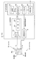
第1の実施形態の表示装置について図1を用いて説明する。図1は、第1の実施形態の表示装置の構成の一例を示した図である。
図1に示した表示装置1は、タッチパネル2と、画像表示パネル3と、制御装置4と、指示装置5と、検出補助装置6と、を有する。
[First Embodiment]
A display device according to a first embodiment will be described with reference to FIG. FIG. 1 is a diagram illustrating an example of the configuration of the display device according to the first embodiment.
The
タッチパネル2は、駆動電極2aと、駆動電極2aの少なくとも一部と誘電体を挟んで対向する検出電極2bとを備え、タッチ面側に検出電極2bが配置される。タッチパネル2では、このような駆動電極2aと検出電極2bとが、タッチ面領域をカバーして複数配置される。以下では、一部分が交差して対向部を形成する駆動電極2aと検出電極2bについて説明するが、他の駆動電極及び検出電極についても同様である。
The
駆動電極2aと検出電極2bとが対向する対向部は、駆動電極2a、誘電体及び検出電極2bにより第1の容量を有する。駆動電極2aに矩形波の駆動信号Txを印加すると、駆動信号Txに同期して検出電極2bにおいて検出信号Rxを検出することができる。すなわち、駆動電極2aに駆動信号Txが印加されると、検出電極2bには駆動電極−検出電極間の相互容量に応じた電荷が蓄えられる。この検出電極2bの電荷量を検出信号Rxとして取り出せば、駆動電極−検出電極間の相互容量を測定することができる。タッチパネル2に指示装置5が接触または近接しているときと、離れているときとでは相互容量が異なるため、相互容量を測定することにより、指示装置5のタッチの有無も検出できる。図1では、駆動電極2aと検出電極2bはタッチパネル2の互いに直交する方向に延在する帯状の形状を有し、その交差する部分に対向部が形成されているが、本発明はこれに限定されない。
The facing portion where the drive electrode 2a and the detection electrode 2b face each other has a first capacitance due to the drive electrode 2a, the dielectric, and the detection electrode 2b. When a rectangular-wave drive signal Tx is applied to the drive electrode 2a, the detection signal Rx can be detected at the detection electrode 2b in synchronization with the drive signal Tx. That is, when the drive signal Tx is applied to the drive electrode 2a, charges corresponding to the mutual capacitance between the drive electrode and the detection electrode are stored in the detection electrode 2b. By taking out the charge amount of the detection electrode 2b as the detection signal Rx, the mutual capacitance between the drive electrode and the detection electrode can be measured. Since the mutual capacitance differs between when the
画像表示パネル3は、平面状の表示面を備え、制御装置4から出力される表示用信号に基づいて画像を表示する。
制御装置4は、画像表示パネル3、駆動電極2a及び検出電極2bに接続し、画像表示パネル3に表示を行う表示制御と、指示装置5のタッチを検出する検出制御と、を行う。検出制御では、駆動電極2aに矩形波の駆動信号Txを印加し、検出電極2bから検出信号Rxを取得する。検出電極2bからは、駆動信号Txの電位変化タイミングに同期した立上り及び立下りの波形を持つ検出信号Rxが出力される。
The
The
指示装置5は、タッチパネル2のタッチ面上の位置を指示する。タッチパネル2に接触または近接した指示装置5は、タッチパネル2と電気的に接続され、第2の容量を形成する。接触または近接したタッチパネル2の検出電極2bを介して入力する駆動信号Txを検知した検出駆動信号Tdを検出補助装置6に出力する。また、検出補助装置6から反転信号RTdを取得し、指示装置5の出力回路と検出電極2b間の容量結合等により、検出電極2bに出力する。
The
検出補助装置6は、反転回路6aを有し、指示装置5から検出駆動信号Tdを取得し、検出駆動信号Tdの位相を反転した反転信号RTdを生成して指示装置5に出力する。なお、検出補助装置6は、他の装置内に設けるとしてもよい。例えば、指示装置5、あるいは制御装置4に設けることができる。
The detection assisting device 6 has an inverting
このような表示装置1のタッチ検出動作について説明する。以下では、指示装置5がタッチパネル2に接触または近接している状態を「タッチ状態」とし、接触も近接もしていない状態を「非タッチ状態」として説明する。
Such a touch detection operation of the
指示装置5が非タッチ状態では、駆動電極2aと検出電極2bとの間の相互容量は、第1の容量に相当する。制御装置4によって駆動電極2aに駆動信号が印加されると、駆動電極−検出電極間に第1の容量に応じた電界が発生する。一方、指示装置5がタッチ状態では、指示装置5との間の第2の容量によって電界の一部が指示装置5との間でも発生する。これにより、駆動電極−検出電極間の電界は減少し、相互容量も減少する。さらに、検出補助装置6から指示装置5を介して駆動信号Txとは逆位相の反転信号RTdが検出電極2bに出力される。この反転信号RTdは、指示装置5と検出電極2bとの容量結合を介して、指示装置5による検出信号Rxの信号変化を助ける方向に働く。
When the
このように、検出信号Rxには、駆動電極−検出電極間の相互容量に応じた信号成分(検出信号Rx0とする)に反転信号RTdによる信号成分が重畳されている。このため、単に駆動電極−検出電極間の相互容量に応じた検出信号Rx0より信号強度が増強される。制御装置4においては、このように信号強度が増強された検出信号Rxを用いて指示装置5のタッチ状態を検出することにより、タッチの有無を確実に検出することが可能となる。
As described above, in the detection signal Rx, the signal component based on the inverted signal RTd is superimposed on the signal component (referred to as the detection signal Rx0) corresponding to the mutual capacitance between the drive electrode and the detection electrode. For this reason, the signal intensity is increased more than the detection signal Rx0 corresponding to the mutual capacitance between the drive electrode and the detection electrode. In the
[第2の実施形態]
次に、第2の実施形態の表示装置について説明する。
図2は、第2の実施形態の表示装置の構成の一例を示した図である。
[Second Embodiment]
Next, a display device according to a second embodiment will be described.
FIG. 2 is a diagram illustrating an example of the configuration of the display device according to the second embodiment.
第2の実施形態の表示装置10は、タッチパネル20と、画像表示パネル30と、表示制御回路35と、タッチパネル制御回路(以下、TPICとする)40と、スタイラス50と、制御装置60と、を有する。表示制御回路35、TPIC40及び制御装置60は、それぞれ、図1に示した制御装置4の処理の一部を実行する。また、図1に示した検出補助装置6は、スタイラス50内に検出補助回路51として搭載される。
The
タッチパネル20は、図2の左右方向に延在する複数の帯状の駆動電極21と、駆動電極21の延在方向と直交する方向に延びる複数の帯状の検出電極22と、を有する相互容量検出方式のタッチパネルである。検出電極22は、タッチパネル20のタッチ面側に配置され、誘電体を挟んでその下層に駆動電極21が配置される。駆動電極21と検出電極22とは平面視で交差しており、その交差部分において駆動電極21と検出電極22とが対向する対向部が形成される。この対向部がタッチセンサとして機能し、タッチパネル20では、対向部がマトリクス状に配置されることにより、スタイラス50のタッチ位置が検出可能となっている。TPIC40は、検出したスタイラス50のタッチの有無と、タッチが検出されたときはその位置と、を含むタッチ情報を制御装置60に出力する。
The
画像表示パネル30は、タッチパネル20と一体化された、いわゆるインセル型で構成される。インセル型の構成では、タッチパネル20の駆動電極21と、液晶表示素子の共通電極と、が共用される。なお、タッチパネル20と画像表示パネル30とは、それぞれ別々に形成した後、接着剤などで貼り合せた構成であってよい。
表示制御回路35は、制御装置4の処理機能のうち、表示制御を行う。制御装置60から画像信号を入力して表示用信号を生成し、画像表示パネル30の表示制御を行う。
The
The
TPIC40は、制御装置4の処理機能のうち、スタイラス50によるタッチを検出する検出制御を行う。TPIC40は、制御装置60からの指示に応じて、駆動電極21を順次選択して交流矩形波の駆動信号を供給し、そのときの検出電極22の検出信号に基づき、スタイラス50のタッチの有無と、タッチ状態であるときはその位置とを検出する。
Of the processing functions of the
スタイラス50は、指示装置5の一実施形態であり、第2の実施形態では、スタイラス50は検出補助回路51を備える。検出補助回路51は、スタイラス50の先端がタッチパネル20に近づいたときに検出される駆動信号Txに応じた検出駆動信号Tdに基づき、駆動信号Txとは逆相の補助信号ARxを生成し、検出電極22に出力する。補助信号ARxは、図1に示した反転信号RTdを含む検出信号Rxの信号強度を強化するための信号を指す。
制御装置60は、表示装置10全体を制御する。
The stylus 50 is an embodiment of the
The
このような表示装置10の各部について説明する。
まず、装置全体を制御する制御装置60について説明する。図3は、第2の実施形態の制御装置の構成の一例を示した図である。
Each part of the
First, the
制御装置60は、CPU(Central Processing Unit)61によって制御されている。CPU61には、バス83を介してRAM(Random Access Memory)62及びROM(Read Only Memory)63と複数の周辺機器が接続されている。
The
RAM62は、制御装置60の主記憶装置として使用される。RAM62には、CPU61に実行させるOS(Operating System)のプログラムやアプリケーションプログラムの少なくとも一部が一時的に格納される。また、RAM62には、CPU61による処理に必要な各種データが格納される。
The
ROM63は、不揮発性の半導体メモリであり、制御装置60の二次記憶装置として使用され、更新する必要のない情報を記憶する。例えば、OSのプログラム、アプリケーションプログラム、及び各種データが格納される。なお、二次記憶装置としては、フラッシュメモリなどの半導体記憶装置を使用することもできる。
The
バス83に接続されている周辺機器としては、表示制御回路35、TPIC40及び通信インタフェース81がある。
表示制御回路35には、画像表示パネル30が接続されている。
Peripheral devices connected to the
An
TPIC40には、タッチパネル20が接続されている。TPIC40は、CPU61の命令に基づいて、スタイラス50のタッチ状態を検出する。また、タッチ位置の座標を算出し、タッチ位置の座標を含むタッチ情報を、バス83を介してCPU61に出力する。
The
通信インタフェース81は、ネットワーク90に接続され、ネットワーク90を介して、他のコンピュータまたは通信機器との間でデータの送受信を行う。また、スタイラス50がネットワーク90に接続すれば、ネットワーク90を介してスタイラス50との間でデータの送受信を行うとしてもよい。
以上のような構成によって、制御装置60の処理機能を実現することができる。
The
With the above configuration, the processing function of the
次に、TPIC40の構成について説明する。図4は、第2の実施形態のTPICの構成の一例を示した図である。図4には、TPIC40とともにタッチパネル20の対向部の断面の概略を示している。
Next, the configuration of the
TPIC40は、駆動制御回路41と、A/D(アナログ/デジタル)変換回路42と、信号処理回路43と、を有し、スタイラス50のタッチを検出する検出制御を行う。タッチを検出したときは、そのタッチ位置の座標を検出し、制御装置60へ通知する。駆動制御回路41は、所定の周波数の交流矩形波の駆動信号Txを駆動電極21に印加する。A/D変換回路42は、駆動制御回路41と同期して動作し、駆動電極−検出電極間の相互容量と、補助信号ARxとに応じた検出信号Rxを入力し、検出データVdetに変換する。A/D変換回路42は、検出電極22ごとに設けられ、対応する検出電極22の検出信号Rxをデジタルデータに変換する変換処理を行う。信号処理回路43は、各A/D変換回路42が変換処理を行った検出データVdetを入力し、タッチ面全体の検出データVdetに基づいて、スタイラス50のタッチ検出と、そのタッチ位置の座標を特定する処理を行う。
The
各処理部を信号の流れに沿って説明する。
駆動制御回路41は、1フレーム期間中の画像表示パネル30の共通電極として共用される駆動電極21が共通電極として動作していない期間に、複数の駆動電極21に対し、順番に駆動信号Txを印加する。例えば、図2に示した駆動電極21を、#1、#2、#3、#4、#5・・・の順に選択し、順次駆動信号Txを印加する。各駆動電極21には、1フレーム期間内に駆動信号Txが複数回印加される。駆動信号Txの印加は、選択した駆動電極21に対し連続的に複数回行うとしてもよい。
Each processing unit will be described along the signal flow.
The
タッチパネル20では、駆動電極21に印加された駆動信号Txによって駆動電極21と検出電極22との間の相互容量に応じた電流が検出電極22に流れる。図4に示したように、駆動電極21と検出電極22との対向部には駆動電極21及び検出電極22と、その間の誘電体とによって静電容量C1(以下、容量C1とする)が形成されている。スタイラス50が非タッチ状態では、駆動電極21に交流矩形波の駆動信号Txを印加したとき、検出電極22に容量C1に応じた電流が流れ、検出信号RxとしてA/D変換回路42に出力される。一方、スタイラス50がタッチ状態では、容量C1にスタイラス50との間に形成される容量C2が直列に追加された形となる。このとき駆動電極21に交流矩形波の駆動信号Txを印加すると、駆動電極−検出電極間とともに、駆動電極−スタイラス間にも電界が生じ、駆動電極−検出電極間の電界は非タッチ状態より減少する。従って、検出信号Rx0は、非タッチ状態よりも小さな値になる。さらに、スタイラス50からは、検出補助回路51で生成された補助信号ARxが検出電極22に出力される。これにより、検出信号Rx0に補助信号ARxの信号成分が重畳されて信号変化が強められた検出信号Rxが得られる。このように、スタイラス50から出力される補助信号ARxは、スタイラス50が駆動電極21との間に形成する容量による検出信号Rxの信号変化を強め、非タッチ状態における検出信号Rxとの差をより顕著にする。検出信号Rxは、複数の検出電極22においてそれぞれ生成され、A/D変換回路42に出力される。
In the
A/D変換回路42は、積分回路421、ADC(Analog to Digital Converter)422及びFIR(Finite Impulse Response)423を有し、駆動制御回路41と同期して検出信号Rxを取り出し、検出信号Rxから信号処理回路43で用いる検出データVdetを生成する。なお、図4では1つのA/D変換回路42のみを示したが、A/D変換回路42は複数の検出電極22それぞれに対応して設けられる。あるいは、複数の検出電極22と、A/D変換回路42とを、例えばマルチプレクサを介して接続し、駆動制御回路41の選択した駆動電極21に合わせて、検出信号の入力先の検出電極22を順次切り替えるとしてもよい。
The A / D conversion circuit 42 includes an
積分回路421は、検出信号Rxを積算した電圧値を出力する。スタイラス50が非タッチ状態では、駆動電極21に駆動信号が印加されると、駆動電極21、容量C1、検出電極22、積分回路421の容量の経路で電流が流れ、積分回路421の出力電圧が低下する。これに対し、スタイラス50がタッチ状態であるときは、駆動電極−検出電極間の容量が小さくなるとともに、スタイラス50の出力信号が加わり、積分回路421に流れ込む電流は小さくなり、積分回路421の出力電圧の降下に差が生じる。
The
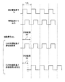
図5は、駆動信号に対する積分回路の出力信号の一例を示した図である。
(A)は、駆動信号Txの交流矩形波の1クロック区間の波形を示している。(B)は、スタイラス50が非タッチ状態のときの積分回路出力電圧の波形を示している。(C)は、スタイラス50がタッチ状態のときの積分回路出力電圧の波形を示している。(B)、(C)ともに、(A)の1クロック区間に対応する。
FIG. 5 is a diagram illustrating an example of an output signal of the integration circuit with respect to the drive signal.
(A) has shown the waveform of 1 clock area of the alternating current rectangular wave of the drive signal Tx. (B) shows the waveform of the integration circuit output voltage when the stylus 50 is in the non-touch state. (C) shows the waveform of the output voltage of the integration circuit when the stylus 50 is in the touch state. Both (B) and (C) correspond to one clock interval of (A).
図5に示したように、駆動信号Txの立上りでは、駆動電極21、相互容量、検出電極22、積分回路421の容量の経路で電流が流れ、積分回路421の出力電圧が降下する。駆動信号Txの立下りでは、逆になる。
As shown in FIG. 5, at the rise of the drive signal Tx, a current flows through the path of the
ここで、(B)に示したスタイラス50が非タッチ状態における積分回路出力電圧の負方向の最大値をベースラインVbとする。同様に、(C)に示したスタイラス50がタッチ状態における積分回路出力電圧の負方向の最大値をVxとする。前述のように、相互容量の大きさは、非タッチ状態>タッチ状態であり、さらに、タッチ状態においてはスタイラス50から検出電極22に駆動信号とは逆相の補助信号ARxが出力される。従って、非タッチ状態におけるベースラインVbと、タッチ状態におけるVxとの差は、タッチ状態/非タッチ状態の判定に用いるのに十分な大きさとなる。第2の実施形態では、タッチ状態と非タッチ状態との積分回路出力電圧の差(図5では、信号成分Vs)に基づいて、タッチ状態であるか非タッチ状態であるかを判定する。なお、図5に示したように、駆動信号の立下り時においても同様に信号成分を検出することができる。
Here, the maximum value in the negative direction of the integration circuit output voltage when the stylus 50 shown in FIG. Similarly, the maximum value in the negative direction of the integration circuit output voltage when the stylus 50 shown in FIG. As described above, the magnitude of the mutual capacitance is a non-touch state> touch state, further auxiliary signal ARx opposite phases are output from the drive signal to the
図4に戻って説明する。
ADC422は、サンプル/ホールド回路を有し、積分回路421において積分が完了した信号のピーク値をサンプル/ホールドし、サンプル/ホールドしたピーク値にA/D変換を施してデジタル信号に変換する。ADC422によって、図5に示した非タッチ状態におけるVbと、タッチ状態におけるVxとが算出される。
FIR423は、平均化処理を行ってADC422が生成した信号に含まれる不要なノイズを低減する。
Returning to FIG.
The
The
このようにして、A/D変換回路42では、駆動電極21に駆動信号Txを印加したときに検出電極22から出力される検出信号Rxに基づいて、検出データVdetが生成される。検出データVdetは、その時点における駆動電極−検出電極間の相互容量を示すものである。相互容量の大きさは、非タッチ状態>タッチ状態であり、これに応じて非タッチ状態とタッチ状態とでは検出データVdetの大きさが異なる。計測した検出データVdetは、信号処理回路43に出力される。
In this manner, the A / D conversion circuit 42 generates the detection data Vdet based on the detection signal Rx output from the
駆動制御回路41は、駆動電極21に選択的に駆動信号Txを印加し、A/D変換回路42では、駆動信号Txの印加に同期してすべての検出電極22において検出データVdetが生成される。この処理を全駆動電極21について行って、タッチパネル20に形成される対向部すべての検出データVdetが生成される。
The
信号処理回路43は、ベースライン記憶部431と、信号値算出部432と、ノイズ検出部433と、座標計算部434と、を有する。信号処理回路43には、駆動電極21と検出電極22とが対向する全対向部における検出データVdetが入力する。
The signal processing circuit 43 includes a
ベースライン記憶部431は、スタイラス50が非タッチ状態におけるA/D変換回路42の検出データVdetをベースラインVbとして記憶する。ベースラインVbは、信号算出部432によって適宜更新される。
The
信号値算出部432は、A/D変換回路42から取得した検出データVdetと、ベースライン記憶部431に記憶されるベースラインVbとに基づいて、検出データVdetに含まれるスタイラス50の存在に起因する信号成分Vsを算出し、スタイラス50がタッチ状態であるか非タッチ状態であるかを判定する。具体的には、A/D変換回路42から取得した検出データVdetと、ベースラインVbとの差分(Vdet−Vb)を算出し、算出した信号値Vsを閾値と比較する。信号値Vsが閾値以下であれば、スタイラス50は非タッチ状態であると判定する。閾値を超えていれば、スタイラス50はタッチ状態であると判定する。また、非タッチ状態であると判定したときは、このときの検出データVdetの値でベースラインVbを更新するとしてもよい。ベースラインVbを適宜更新することによって、動作環境の変化などによってベースライン値がずれてしまった場合にも対応が可能であり、正確なタッチ検出を行うことができる。
The signal
ノイズ検出部433は、信号値算出部432が算出したタッチ面領域の信号値Vsを解析し、タッチ面領域の信号値Vsにノイズが含まれているか否かを判定する。例えば、ACチャージャーノイズなど、想定されるノイズパターンと、タッチ面領域の信号値Vsとを比較し、ノイズパターンが検出されるか否かで判定する。ノイズを検出した場合には、駆動制御回路41に対し駆動信号Txの周波数の変更を指示するようにしてもよい。
The
座標計算部434は、算出された信号値Vsがタッチ状態を示すとき、タッチ状態を示した位置座標の検出処理を行う。ノイズ検出部433によってノイズが除去された信号値Vs(=Vdet−Vb)を用いて、タッチ状態を示す対向部の分布状況を解析し、位置座標を決定する。位置座標の決定方法は、動作状態等に応じて適宜選択される。例えば、対向部がタッチ状態を示す領域の重心を求め、位置座標としてもよい。あるいは、算出された信号値Vsの値が高いものに基づいて位置座標を決めるとしてもよい。また、必要に応じて、前回検出した位置座標と関連付ける追跡処理を行うとしてもよい。算出したタッチの有無と、タッチの位置座標とは、タッチ情報として制御装置60へ出力する。
なお、第2の実施形態では、信号処理回路43をTPIC40内に設けたが、同様の処理を制御装置60で行うとしてもよい。また、信号処理回路43の一部の処理を制御装置60で行うとしてもよい。
When the calculated signal value Vs indicates the touch state, the coordinate
Although the signal processing circuit 43 is provided in the
次に、スタイラスについて説明する。図6は、第2の実施形態のスタイラスの構成の一例を示した図である。
スタイラス50は、検出補助回路51と、ペン先検出部52と、ペン先出力部53と、を有する。
Next, the stylus will be described. FIG. 6 is a diagram illustrating an example of the configuration of the stylus according to the second embodiment.
The stylus 50 includes a detection
検出補助回路51は、反転回路511と、増幅回路512と、を有する。反転回路511は、ペン先検出部52から入力した検出駆動信号Tdの電位変化を反転し、反転信号を生成する。増幅回路512は、反転回路511から入力した反転信号を所定のゲインで増幅した増幅反転信号を生成し、増幅反転信号を補助信号ARxとしてペン先出力部53へ出力する。
The detection
ペン先検出部52は、タッチパネル20に向けられるスタイラス50の先端部分に形成される。そして駆動電極21に印加された駆動信号Txの電位変動を検知し、検出駆動信号Tdを反転回路511に出力する。
The pen
ペン先出力部53は、ペン先検出部52と同様に、スタイラス50の先端部分に形成される。そして、増幅回路512によって生成された補助信号ARxを、検出電極22に出力する。
Similar to the pen
このような構成のスタイラス50は、タッチパネル20に近づくと、ペン先検出部52を介してタッチパネル20の駆動信号Txの電位変動が検出される。検出した検出駆動信号Tdの信号レベルは、スタイラス50と検出電極22との間の距離が同じであれば、検出電極22と駆動信号Txが印加された駆動電極21との距離に応じて決まる。例えば、図2に示した駆動電極21の#1〜#5のうち、#3の近傍にスタイラス50が近接していたとする。#1から順に駆動信号Txを印加していくと、スタイラス50で検出される検出駆動信号Tdの電位レベルは、#3に駆動信号Txが印加されたときに最大となり、駆動信号Txが印加される位置が#3から離れるほど、電位レベルは小さくなる。スタイラス50では、このように検出された電位変化を検出補助回路51で反転・増幅した補助信号ARxをペン先出力部53から出力する。従って、補助信号ARxは、駆動信号Txが離れたところに印加している場合は弱く、近いところに印加している場合は強く信号変化を助けるため、検出信号Rxの信号強度を増強させることができる。
When the stylus 50 having such a configuration approaches the
このように、表示装置10では、相互容量方式のタッチパネル20における操作入力にこのようなスタイラス50を用いることにより、検出信号Rxの信号強度を増強することが可能となる。これにより、タッチ状態と非タッチ状態の信号変化の差が大きくなり、接触面積の小さいスタイラス50であっても、タッチの有無を確実に検出することができる。また、よりタッチ位置に近い駆動電極21において信号強度を増強させるため、タッチ位置をより確実に検出することができる。特に、インセル型のタッチパネルの場合、駆動電極21と検出電極22との距離が大きくなるため、検出電極22に届く駆動信号Txが小さくなり、タッチ検出が難しい。しかしながら、表示装置10によれば、信号強度を増強させることができるため、インセル型のタッチパネルでも確実にタッチを検出することができる。
As described above, in the
なお、増幅回路512のゲインは、補助信号ARxの電位レベルが最適となるように適宜設定される。また、スタイラス50がタッチ面に接触しているか否かにより、増幅回路512のゲインの設定を切り換えるようにしてもよい。例えば、ペン先検出部52に圧力検出機構を設け、スタイラス50のペン先がタッチ面に接触しているか否かを検出する。検出している場合と、タッチ面の上空に存在している場合とでは、増幅回路512のゲインを切り換えて増幅の度合いを変え、上空にあるときの指示入力を制御する。上空にあるときのゲインを下げれば、スタイラス50がタッチ面に接触していなければ指示入力ができなくなり、誤入力を防止できる。一方、ゲインを上げれば、上空での指示入力を確実に行うことができる。
Note that the gain of the amplifier circuit 512 is appropriately set so that the potential level of the auxiliary signal ARx is optimized. Further, the gain setting of the amplifier circuit 512 may be switched depending on whether the stylus 50 is in contact with the touch surface. For example, a pressure detection mechanism is provided in the pen
ところで、検出駆動信号Tdは、駆動電極21に印加された駆動信号Txが誘電体、検出電極22、スタイラス−検出電極間容量という経路を通ってスタイラス50に入力する。このため、経路途中でノイズが混入する場合がある。例えば、表示装置10に低コストの充電器を接続したときに充電器から発生するノイズ、いわゆるACチャージャーノイズが付加されることが考えられる。
By the way, the detection drive signal Td is input to the stylus 50 through the path of the dielectric, the
図7は、ノイズパターンの一例を示した図である。
図7に示した黒い領域がスタイラス50のタッチを検出した箇所を示す。図7の例では、(A)ノイズ無パターンの一例、(B)ノイズ有パターンの一例とも、タッチパネル20の同じ位置にスタイラス50をタッチしている。
FIG. 7 is a diagram illustrating an example of a noise pattern.
The black area shown in FIG. 7 indicates a location where the touch of the stylus 50 is detected. In the example of FIG. 7, the stylus 50 is touched at the same position on the
(A)ノイズ無パターンの一例に示すノイズ無の場合、領域P1の1箇所のみでタッチが検出されている。この領域P1がスタイラス50によってタッチされている箇所であり、このようなパターンであれば、タッチ位置の座標を容易に算出することができる。
これに対し、(B)ノイズ有パターンの一例に示すノイズ有の場合、領域P2の周りに複数の領域N1、N2、N3、N4にタッチが検出されている。領域P2がスタイラス50によってタッチされている箇所であり、領域N1、N2、N3、N4はノイズである。このようなパターンが発生した状態では、タッチ位置の検出精度が低下する。
(A) In the case of no noise shown in an example of a noiseless pattern, a touch is detected only at one location in the region P1. This area P1 is a place touched by the stylus 50. With such a pattern, the coordinates of the touch position can be easily calculated.
On the other hand, in the case of the presence of noise shown in the example of the (B) noisy pattern, the touch is detected in the plurality of areas N1, N2, N3, and N4 around the area P2. The region P2 is a place touched by the stylus 50, and the regions N1, N2, N3, and N4 are noises. When such a pattern is generated, the detection accuracy of the touch position decreases.
そこで、表示装置10では、信号処理回路43において、検出信号Rxから得た信号値Vsを解析し、ノイズの検出と、ノイズを軽減する処理を行う。
ノイズ検出部433では、信号値算出部432より取得したタッチパネル20のタッチ面全体のタッチ情報と、ACチャージャーノイズなど、予め予測されるノイズパターンと、を比較し、ノイズが発生しているか否かを判定する。ノイズが発生していると判断したときは、このようなノイズによるタッチ位置検出精度の低下を防ぐため、表示装置10では、駆動信号Txの周波数を切り換え、新たな駆動信号周波数Txfを駆動制御回路41に通知する。ACチャージャーノイズなど、周期的に発生するノイズの周波数と、駆動信号Txの周波数とが近い場合、検出信号Rxにノイズが重畳されてしまう。そこで、駆動信号Txの周波数を切り換え、ACチャージャーノイズの周波数と異ならせることにより、駆動信号とノイズを区別し、検出信号Rxに重畳するノイズを軽減することができる。
Therefore, in the
In the
このような構成の表示装置10におけるタッチ検出処理について、フローチャートを用いて説明する。図8は、第2の実施形態の表示装置のタッチ検出処理を示したフローチャートである。表示装置10が動作を開始し、タッチ検出処理を起動してTPIC40による処理が開始される。
The touch detection process in the
[ステップS01]TPIC40は、立上り時に、駆動信号周波数Txfに予め決められた初期値を設定し、駆動信号Txの周波数を初期設定する。
[ステップS02]TPIC40は、タッチ検出を行う処理期間であるか否かを判定する。タッチ検出は、駆動電極21が表示用の共通電極として動作していない期間に行われる。処理期間であれば、処理をステップS03に進める。処理期間でなければ、次の処理期間の開始まで待つ。
[Step S01] At the time of rising, the
[Step S02] The
[ステップS03]TPIC40は、処理期間であるのでタッチ検出処理を行う。タッチ検出処理では、駆動制御回路41によって駆動電極21に順次駆動信号Txを印加し、検出電極22から検出信号Rxを入力する。入力した検出信号Rxは、A/D変換回路42によって検出データVdetに変換される。タッチ検出処理では、駆動電極21と検出電極22とが交差する全ての対向部における検出データVdetを求める。
[Step S03] Since the
[ステップS04]TPIC40は、立ち上げ時の処理であるか否かを判定する。立ち上げ時であれば、処理をステップS05に進める。立ち上げ時でなければ、処理をステップS06に進める。
[Step S04] The
[ステップS05]TPIC40は、立ち上げ時の処理であるので、検出データVdetの値をベースラインVbに設定し、ベースライン記憶部431に記憶する。ベースラインVbには、スタイラス50が非タッチ状態にあると推定される検出データVdetが設定される。
[Step S05] Since the
[ステップS06]TPIC40は、ベースライン記憶部431に記憶するベースラインVbと、タッチ検出処理によって得られた検出データVdetを用いて信号成分Vsを算出する。信号成分Vsは、検出データVdetとベースラインVbとの差分(Vs=Vdet−Vb)を算出して得る。
[Step S06] The
[ステップS07]TPIC40は、算出した信号成分Vsと閾値とを比較する。信号成分Vsと閾値との比較は、対向部ごとに算出された信号成分Vs全てについて行う。信号成分Vs>閾値が成立するものがあるときは、処理をステップS08に進める。信号成分Vs>閾値が成立するものがないときは処理をステップS11に進める。
[Step S07] The
[ステップS08]TPIC40は、信号成分Vsが閾値より大きいとき、得られた検出データVdetと予め登録されたノイズパターンとを照合し、検出データVdetにノイズが含まれているか否かを判定する。ノイズ有と判定したときは、処理をステップS12に進める。ノイズ無と判定したときは、処理をステップS09に進める。
[Step S08] When the signal component Vs is larger than the threshold value, the
[ステップS09]TPIC40は、ノイズ無と判定したときは、信号成分Vsに基づいてタッチ位置の座標値を計算する。
[Step S09] When the
[ステップS10]TPIC40は、算出したタッチ位置の座標値を制御装置60に出力し、処理をステップS02に進める。
[ステップS11]TPIC40は、信号成分Vsが閾値未満であるとき、検出データVdetは非タッチ状態を示していると判定する。新たな検出データVdetをベースラインVbとしてベースライン記憶部431を更新し、処理をステップS02に進める。
[Step S10] The
[Step S11] When the signal component Vs is less than the threshold value, the
[ステップS12]TPIC40は、ノイズ有と判定したときは、ノイズを軽減するため、駆動信号Txの周波数(駆動信号周波数Txf)を異なる値に切り換え、処理をステップS02に進める。
[Step S12] When the
以上の処理手順が実行されることにより、TPIC40では、タッチパネル20にスタイラス50がタッチしたことを検出し、タッチした位置の座標値を得る。スタイラス50がタッチパネル20にタッチした状態では、スタイラス50から駆動信号Txとは逆位相の補助信号ARxが検出電極22に出力されるので、スタイラス50が補助信号ARxを出力しない場合と比較し、信号成分Vsが大きな値となる。このため、タッチの有無を確実に検出することが可能となる。
また、得られた信号成分Vsにノイズパターンが検出されたときは、駆動信号Txの周波数を切り換えノイズ低減を図る。これにより、ACチャージャーノイズなどのノイズによる影響を軽減することができる。
By executing the above processing procedure, the
When a noise pattern is detected in the obtained signal component Vs, the frequency of the drive signal Tx is switched to reduce noise. Thereby, the influence by noise, such as AC charger noise, can be reduced.
なお、上記では、スタイラス50を用いてタッチパネル20に入力操作を行う場合について説明した。しかし、タッチパネル20は、相互容量方式のタッチパネルであり、指をタッチ面に接触または近接して操作できることは当然である。この場合、指はタッチ面に充分な接触面積を確保できることから、補助信号ARxが検出電極22に出力されなくてもタッチの有無を確実に検出できる。
In the above description, the case where an input operation is performed on the
[第3の実施形態]
第2の実施形態では、ACチャージャーノイズなどのノイズを軽減するため、ノイズパターンが検出されたときには、TPIC40において駆動信号周波数Txfを切り換えるとしていた。第3の実施形態では、さらに、スタイラス50においてノイズを軽減する処理を行う。
[Third Embodiment]
In the second embodiment, in order to reduce noise such as AC charger noise, the drive signal frequency Txf is switched in the
以下、第3の実施形態の表示装置について図9を用いて説明する。第3の実施形態では、第2の実施形態のスタイラス50の検出補助回路51を新たな構成に置き換える。他の構成は第2の実施形態と同様であるので、新たな検出補助回路についてのみ説明する。
Hereinafter, a display device according to a third embodiment will be described with reference to FIG. In the third embodiment, the detection
図9は、第3の実施形態の表示装置の第2検出補助回路の構成の一例を示した図である。
第3の実施形態の第2検出補助回路54は、第2の実施形態の検出補助回路51を置き換えたものであり、検出補助回路51と同じものには同じ番号を付し、説明は省略する。
第2検出補助回路54は、周波数選択回路541と、反転回路511と、増幅回路512と、増幅回路542と、加算器(加算回路)543と、を有する。
FIG. 9 is a diagram illustrating an example of the configuration of the second detection auxiliary circuit of the display device according to the third embodiment.
The second detection auxiliary circuit 54 of the third embodiment replaces the detection
The second detection auxiliary circuit 54 includes a
周波数選択回路541は、入力した検出駆動信号Tdに含まれる信号成分の周波数が駆動信号周波数Txfであるか、それ以外の周波数であるかに応じて、信号成分ごとに出力先を選択する。信号成分には、まず、検出駆動信号Tdに含まれる駆動信号Txに応じた信号成分がある。ノイズが発生していないときは、検出駆動信号Tdに含まれる信号成分は、駆動信号Txに応じた信号成分のみになる。この周波数が駆動信号周波数Txfと一致する信号成分を便宜的に第1の信号とする。ノイズが発生している場合、検出駆動信号Tdには、第1の信号に加え、ノイズ成分が含まれる。ノイズによる信号は、駆動信号周波数Txfとは異なる周波数を有する。この信号を第2の信号とする。このような周波数の違いに基づき、周波数選択回路541では検出駆動信号Tdの信号成分を周波数によって分類し、第1の信号は反転回路511に出力し、第2の信号は増幅回路542に出力する。
The
反転回路511及び増幅回路512は、入力した検出駆動信号Tdに含まれる第1の信号の電位変化を反転し、増幅した後、加算器543に出力する。
増幅回路542は、入力した検出駆動信号Tdに含まれる第2の信号の電位変化をそのままの状態で増幅した後、加算器543に出力する。電位変化をそのままの状態で増幅した信号成分は、検出電極22に出力されたとき、駆動信号Txに含まれるノイズを削減する補正信号になる。
The inverting
The amplifier circuit 542 amplifies the potential change of the second signal included in the input detection drive signal Td as it is, and then outputs the amplified signal to the
加算器543は、増幅回路512を経由して入力した第1の信号の位相を反転した第1の反転信号と、増幅回路542を経由して入力した補正信号と、を加算した補正反転信号を生成し、補助信号ARxとしてペン先出力部53から出力する。
The
このような第2検出補助回路54によれば、周波数選択回路541において、検出駆動信号Tdに含まれる第1の信号の信号成分と、第2の信号の信号成分と、を分離する。駆動信号Txと同じ周波数の第1の信号については、反転回路511及び増幅回路512によって反転・増幅し、第1の反転信号を生成する。一方、ノイズ成分である第2の信号については、反転せずに、増幅回路542によって増幅し、検出信号Rxに含まれるノイズ成分を補正する補正信号を生成する。加算器543において、第1の反転信号と、補正信号とを加算した補正反転信号を生成し、補助信号ARxとして検出電極22に出力する。このような補助信号ARxが検出電極22に出力されることにより、検出信号Rxに含まれるタッチ検出に関する信号分を増強し、ノイズ成分を減少させることができる。
これにより、ノイズの多い環境下においても確実にタッチの有無を検出することができる。
According to the second detection auxiliary circuit 54, the
Thereby, the presence or absence of a touch can be reliably detected even in a noisy environment.
なお、図8に示したように、ノイズが検出されたときに駆動信号周波数Txfを切り換える構成とした場合、周波数選択回路541では、その時点における駆動信号周波数TxfをTPIC40側からスタイラス50側に通知する必要がある。第2検出補助回路54に駆動信号周波数Txfを通知する機能を設けた構成について説明する。
As shown in FIG. 8, when the drive signal frequency Txf is switched when noise is detected, the
図10は、第3検出補助回路の構成の一例を示した図である。
図10に示した第3検出補助回路55は、第2検出補助回路54に、周波数受信回路551を加えた構成を有する。周波数受信回路551は、検出駆動信号Tdを入力し、検出駆動信号Tdから検出駆動信号Tdに含まれる駆動信号周波数Txfの通知を分離する。そして取得した駆動信号周波数Txfを周波数選択回路541に通知する。周波数選択回路541では、通知を受けた駆動信号周波数Txfを記憶部に記憶しておき、検出駆動信号Tdの周波数による成分分離の際に参照する。
FIG. 10 is a diagram showing an example of the configuration of the third detection auxiliary circuit.
The third detection
TPIC40側では、ノイズ検出部433から新たな駆動信号周波数Txfを取得した駆動制御回路41が、駆動信号周波数Txfを切り換えるとともに、この駆動信号周波数Txfの通知を駆動信号Txに重畳して出力する。
On the
駆動信号周波数Txfの通知は、例えば、図8に示した信号処理の処理手順において、ステップS01の駆動信号周波数Txf初期設定及びステップS12の駆動信号周波数Txf切り換えの後、続けて行う。また、駆動信号周波数Txfの通知は、駆動電極21または検出電極22を介してタッチ検出をしていない期間にデータ通信を行うとしてもよい。駆動信号Txに重畳された駆動信号周波数Txfの通知は、スタイラス50が近づいたとき、駆動電極21、第1容量、検出電極22と流れ、ペン先検出部52から第3検出補助回路55へ入力する。
The notification of the drive signal frequency Txf is performed continuously after the initial setting of the drive signal frequency Txf in step S01 and the switching of the drive signal frequency Txf in step S12, for example, in the signal processing procedure shown in FIG. The notification of the drive signal frequency Txf may be performed through data communication during a period in which touch detection is not performed via the
なお、TPIC40からスタイラス50への駆動信号周波数Txfの転送は、検出電極22とスタイラス50との間の検出駆動信号Tdを介して行う方法に限定されない。例えば、通信インタフェース81を介して行うとしてもよい。
The transfer of the drive signal frequency Txf from the
[第4の実施形態]
第2の実施形態及び第3の実施形態では、スタイラス50内における信号処理による位相遅延については無視できるとしていた。例えば、第2の実施形態では、ペン先検出部52で検知された検出駆動信号Tdは、反転回路511で反転され、増幅回路512で増幅されて補助信号ARxとなった後、ペン先出力部53より出力されるのみであり、スタイラス50内で生じる位相遅延はほとんどないと考えられる。よって、ペン先検出部52で検知する信号と同期して検出電極22で検出される駆動電極−検出電極間の相互容量に応じた信号成分と、補助信号ARxとの位相差は無視できると考えらえる。
[Fourth Embodiment]
In the second and third embodiments, the phase delay due to signal processing in the stylus 50 is negligible. For example, in the second embodiment, the detection drive signal Td detected by the pen
しかしながら、スタイラス50内での位相遅延が大きくなると、検出信号Rxに含まれる検出電極22で検出される駆動電極−検出電極間の相互容量に応じた信号成分と、補助信号ARxの信号成分との位相差が大きくなり、検出信号Rxを用いるTPIC40での誤動作の要因となりうる。
However, when the phase delay in the stylus 50 increases, the signal component corresponding to the mutual capacitance between the drive electrode and the detection electrode detected by the
第4の実施形態は、第1の実施形態の検出補助回路51に、ペン先出力部53から出力される補助信号ARxの位相をペン先検出部52の検出駆動信号Tdの位相に合わせる回路を備える。
In the fourth embodiment, a circuit that matches the phase of the auxiliary signal ARx output from the pen
以下、第4の実施形態の表示装置について図11を用いて説明する。
図11は、第4の実施形態の表示装置の第4検出補助回路の構成の一例を示した図である。
Hereinafter, a display device according to a fourth embodiment will be described with reference to FIG.
FIG. 11 is a diagram illustrating an example of the configuration of the fourth detection auxiliary circuit of the display device according to the fourth embodiment.
図11に示した第4検出補助回路56は、図6に示した検出補助回路51に位相調整回路561を加えた構成である。検出補助回路51と同じものについては、説明を省略する。
The fourth detection auxiliary circuit 56 shown in FIG. 11 has a configuration in which a
位相調整回路561は、ペン先検出部52から入力する検出駆動信号Tdと、増幅回路512が出力する補助信号ARxと、を入力し、検出駆動信号Tdに対する補助信号ARxの位相の遅延を監視する。そして、位相の遅延量が一定量を超えた場合は、補助信号ARxの位相を検出駆動信号Tdに合わせる調整を行う。補助信号ARxの位相をシフトさせ、波形のエッジを次の検出駆動信号Tdのエッジに合わせる。位相の遅延量が一定量を超えない場合は、補助信号ARxの位相をシフトさせずにそのまま出力する。
The
図12は、位相調整回路の入力信号と出力信号との関係を示した図である。1clkは、検出駆動信号Tdの1周期を示している。
図12に示したように、検出駆動信号Tdに対し、増幅回路512の出力には位相遅延が発生している。位相調整回路561には、位相遅延の許容範囲が予め設定されており、この許容範囲に基づいて補助信号ARxの位相を検出駆動信号Tdの位相に合わせるか否かを判定する。
FIG. 12 is a diagram illustrating the relationship between the input signal and the output signal of the phase adjustment circuit. 1 clk indicates one cycle of the detection drive signal Td.
As shown in FIG. 12, a phase delay occurs in the output of the amplifier circuit 512 with respect to the detection drive signal Td. In the
図12(A)位相遅延が許容範囲内の出力は、増幅回路512の出力信号の位相が許容範囲(A)内である場合の位相調整回路561の出力を示している。位相遅延は、許容範囲(A)内であるので、位相遅延は行わず、増幅回路512の出力をそのまま補助信号ARxとして出力する。
12A shows the output of the
図12(B)位相遅延が許容範囲を超えたときの出力は、増幅回路512の出力信号の位相が許容範囲(B)を超えている場合の位相調整回路561の出力を示している。位相遅延は、許容範囲(B)を超えているので、増幅回路512の出力の位相を、1clk後の検出駆動信号Tdのエッジに合わせて遅延し、補助信号ARxとして出力する。
The output when the phase delay exceeds the allowable range in FIG. 12B indicates the output of the
このように、位相調整回路561を設け、補助信号ARxの位相を検出駆動信号Tdの位相に合わせることにより、補助信号ARxの位相が検出電極22における駆動電極−検出電極間の相互容量に応じた信号成分の位相と同期する。これにより、補助信号ARxの位相遅延に起因するTPIC40における誤動作を低減することが可能となる。
なお、第4の実施形態では、位相遅延を検出して位相をシフトさせるとしたが、補助信号ARxの位相を常に、次の検出駆動信号Tdのエッジに合わせて遅延させるとしてもよい。
As described above, the
In the fourth embodiment, the phase delay is detected and the phase is shifted. However, the phase of the auxiliary signal ARx may be always delayed in accordance with the edge of the next detection drive signal Td.
なお、上記の処理機能は、コンピュータによって実現することができる。その場合、表示装置が有すべき機能の処理内容を記述したプログラムが提供される。そのプログラムをコンピュータで実行することにより、上記処理機能がコンピュータ上で実現される。処理内容を記述したプログラムは、コンピュータで読み取り可能な記録媒体に記録しておくことができる。コンピュータで読み取り可能な記録媒体としては、磁気記憶装置、光ディスク、光磁気記録媒体、半導体メモリなどがある。磁気記憶装置には、ハードディスクドライブ(HDD;Hard Disk Drive)、フレキシブルディスク(FD)、磁気テープなどがある。光ディスクには、DVD(Digital Versatile Disc)、DVD−RAM、CD(Compact Disc)−ROM、CD−R(Recordable)/RW(ReWritable)などがある。光磁気記録媒体には、MO(Magneto-Optical disk)などがある。 The above processing functions can be realized by a computer. In that case, a program describing the processing contents of the functions that the display device should have is provided. By executing the program on a computer, the above processing functions are realized on the computer. The program describing the processing contents can be recorded on a computer-readable recording medium. Examples of the computer-readable recording medium include a magnetic storage device, an optical disk, a magneto-optical recording medium, and a semiconductor memory. Examples of the magnetic storage device include a hard disk drive (HDD), a flexible disk (FD), and a magnetic tape. Optical disks include DVD (Digital Versatile Disc), DVD-RAM, CD (Compact Disc) -ROM, CD-R (Recordable) / RW (ReWritable), and the like. Magneto-optical recording media include MO (Magneto-Optical disk).
プログラムを流通させる場合には、例えば、そのプログラムが記録されたDVD、CD−ROMなどの可搬型記録媒体が販売される。また、プログラムをサーバコンピュータの記憶装置に格納しておき、ネットワークを介して、サーバコンピュータから他のコンピュータにそのプログラムを転送することもできる。 When distributing the program, for example, a portable recording medium such as a DVD or a CD-ROM in which the program is recorded is sold. It is also possible to store the program in a storage device of a server computer and transfer the program from the server computer to another computer via a network.
プログラムを実行するコンピュータは、例えば、可搬型記録媒体に記録されたプログラムもしくはサーバコンピュータから転送されたプログラムを、自己の記憶装置に格納する。そして、コンピュータは、自己の記憶装置からプログラムを読み取り、プログラムにしたがった処理を実行する。なお、コンピュータは、可搬型記録媒体から直接プログラムを読み取り、そのプログラムにしたがった処理を実行することもできる。また、コンピュータは、ネットワークを介して接続されたサーバコンピュータからプログラムが転送されるごとに、逐次、受け取ったプログラムにしたがった処理を実行することもできる。 The computer that executes the program stores, for example, the program recorded on the portable recording medium or the program transferred from the server computer in its own storage device. Then, the computer reads the program from its own storage device and executes processing according to the program. The computer can also read the program directly from the portable recording medium and execute processing according to the program. In addition, each time a program is transferred from a server computer connected via a network, the computer can sequentially execute processing according to the received program.
また、上記の処理機能の少なくとも一部を、DSP(Digital Signal Processor)、ASIC(Application Specific Integrated Circuit)、PLD(Programmable Logic Device)などの電子回路で実現することもできる。 In addition, at least a part of the above processing functions can be realized by an electronic circuit such as a DSP (Digital Signal Processor), an ASIC (Application Specific Integrated Circuit), or a PLD (Programmable Logic Device).
本実施形態においては、開示例として液晶表示装置の場合を例示したが、その他の適用例として、有機EL(ElectroLuminescence)表示装置、その他の自発光型表示装置、あるいは電気泳動素子等を有する電子ペーパー型表示装置等、あらゆるフラットパネル型の表示装置が挙げられる。また、中小型から大型まで、特に限定することなく適用が可能であることは言うまでもない。
また、上記第1〜第4の実施形態は製品の仕様等により必要な構成要素を適宜組み合わせて構成してもよい。
In the present embodiment, the case of a liquid crystal display device has been exemplified as a disclosure example. However, as other application examples, an electronic paper having an organic EL ( ElectroLuminescence ) display device, another self-luminous display device, an electrophoretic element, or the like. Any flat panel type display device such as a type display device may be used. Moreover, it cannot be overemphasized that it can apply, without specifically limiting from a small size to a large size.
The first to fourth embodiments may be configured by appropriately combining necessary constituent elements according to product specifications and the like.
本発明の思想の範疇において、当業者であれば、各種の変更例及び修正例に想到し得るものであり、それら変更例及び修正例についても本発明の範囲に属するものと了解される。例えば、前述の各実施形態に対して、当業者が適宜、構成要素の追加、削除若しくは設計変更を行ったもの、または、工程の追加、省略もしくは条件変更を行ったものも、本発明の要旨を備えている限り、本発明の範囲に含まれる。 In the scope of the idea of the present invention, those skilled in the art can conceive various changes and modifications, and it is understood that these changes and modifications also belong to the scope of the present invention. For example, those in which the person skilled in the art has appropriately added, deleted, or changed the design of the above-described embodiments, or those in which processes have been added, omitted, or changed conditions are also the gist of the present invention. As long as it is provided, it is included in the scope of the present invention.
(1)開示される発明の一態様は、
駆動電極と、前記駆動電極の少なくとも一部と誘電体を挟んで対向する検出電極と、を備え、前記駆動電極に印加された駆動信号に同期して前記検出電極から検出信号を出力するタッチパネルと、
前記タッチパネルのタッチ面上の位置を指示する指示装置と、
前記指示装置において検出される前記駆動信号に応じた検出駆動信号を取得し、前記検出駆動信号の位相を反転した反転信号を生成する反転回路を有し、前記反転信号を前記指示装置経由で前記検出電極に出力する検出補助装置と、
前記駆動電極に前記駆動信号を印加し、前記駆動電極と前記検出電極との間の相互容量と、前記反転信号とに応じて前記検出電極に発生する前記検出信号を取得し、前記検出信号に基づいて前記指示装置の前記タッチパネルへの接触または近接を検出する制御装置と、
を有する表示装置である。
(1) One aspect of the disclosed invention is
A touch panel including a drive electrode and a detection electrode facing at least a part of the drive electrode with a dielectric interposed therebetween, and outputting a detection signal from the detection electrode in synchronization with the drive signal applied to the drive electrode; ,
An instruction device for indicating a position on the touch surface of the touch panel;
An inversion circuit that obtains a detection drive signal corresponding to the drive signal detected in the indication device and generates an inversion signal obtained by inverting the phase of the detection drive signal, and the inversion signal is transmitted through the indication device. A detection auxiliary device for outputting to the detection electrode;
Applying the drive signal to the drive electrode, obtaining the detection signal generated in the detection electrode according to the mutual capacitance between the drive electrode and the detection electrode and the inverted signal, and obtaining the detection signal A control device that detects contact or proximity of the pointing device to the touch panel,
It is a display apparatus which has.
(2)開示される発明の一態様は、
前記検出補助装置は、前記指示装置に設けられる、
(1)に記載の表示装置である。
(2) One aspect of the disclosed invention is as follows:
The detection assisting device is provided in the indicating device;
The display device according to (1).
(3)開示される発明の一態様は、
前記検出補助装置は、
前記反転信号を所定のゲインで増幅する増幅回路を有し、前記増幅回路において前記反転信号を増幅した増幅反転信号を前記指示装置経由で前記検出電極に出力する、
(1)または(2)に記載の表示装置である。
(3) One aspect of the disclosed invention is as follows:
The detection assisting device includes:
An amplification circuit that amplifies the inverted signal with a predetermined gain, and outputs an amplified inverted signal obtained by amplifying the inverted signal in the amplifier circuit to the detection electrode via the pointing device;
The display device according to (1) or (2).
(4)開示される発明の一態様は、
前記指示装置は、前記タッチ面に接触しているか否かを検出して検出結果を前記検出補助装置へ通知し、
前記検出補助装置は、前記検出結果に基づき、前記指示装置が前記タッチ面に接触しているときは前記増幅回路に第1のゲインを設定し、前記指示装置が前記タッチ面に接触していないときは前記増幅回路に第2のゲインを設定して、前記増幅反転信号の増幅の度合いを切り換える、
(3)に記載の表示装置である。
(4) One aspect of the disclosed invention is as follows:
The pointing device detects whether the touch surface is touched and notifies the detection assisting device of a detection result;
The detection assisting device sets a first gain in the amplification circuit when the pointing device is in contact with the touch surface based on the detection result, and the pointing device is not in contact with the touch surface. When setting a second gain in the amplifier circuit, the degree of amplification of the amplified inverted signal is switched.
The display device according to (3).
(5)開示される発明の一態様は、
前記検出補助装置は、
前記検出駆動信号に含まれる信号成分と前記駆動信号の周波数とを比較し、周波数が同じ第1の信号を選択して前記反転回路に出力する周波数選択回路と、
前記反転回路によって前記第1の信号の位相が反転された第1の反転信号に、周波数が前記駆動信号の周波数と異なる第2の信号を加算して前記第1の反転信号を補正した補正反転信号を生成する加算回路と、
を有し、前記補正反転信号を前記指示装置経由で前記検出電極に出力する、
(1)乃至(4)の何れか一に記載の表示装置である。
(5) One aspect of the disclosed invention is
The detection assisting device includes:
A frequency selection circuit that compares a signal component included in the detection drive signal with the frequency of the drive signal, selects a first signal having the same frequency, and outputs the first signal to the inverting circuit;
Correction inversion in which the first inverted signal is corrected by adding a second signal having a frequency different from the frequency of the drive signal to the first inverted signal obtained by inverting the phase of the first signal by the inverting circuit. An adder circuit for generating a signal;
And outputting the correction inversion signal to the detection electrode via the pointing device,
(1) It is a display apparatus as described in any one of (4).
(6)開示される発明の一態様は、
前記制御装置は、前記検出信号と、予め定義されたノイズ情報とを照合し、前記検出信号にノイズが含まれると判定したときは、前記駆動信号の周波数を変更し、変更後の変更周波数を前記検出補助装置へ通知するノイズ検出部を有し、
前記検出補助装置は、通知された前記変更周波数を取得し、前記周波数選択回路の前記変更周波数を前記検出駆動信号に含まれる信号成分の選択に用いる、
(5)に記載の表示装置である。
(6) One aspect of the disclosed invention is
The control device collates the detection signal with predefined noise information, and determines that the detection signal contains noise, changes the frequency of the drive signal, and sets the changed frequency after the change. A noise detection unit for notifying the detection assisting device;
The detection assisting device acquires the notified the changed frequency, using said frequency change of said frequency selecting circuit to select a signal component included in the detection drive signal,
The display device according to (5).
(7)開示される発明の一態様は、
前記検出補助装置は、前記指示装置経由で前記検出電極へ出力する補助信号の位相を前記検出駆動信号の位相と比較して、前記検出駆動信号に対する前記補助信号の位相遅延量が所定の許容範囲内であるか否かを判定し、前記位相遅延量が前記許容範囲を超えているときは、前記補助信号の位相を前記検出駆動信号の位相に合わせる位相調整回路を有する、
(1)乃至(6)の何れか一に記載の表示装置である。
(7) One aspect of the disclosed invention is as follows:
The detection auxiliary device compares the phase of the auxiliary signal output to the detection electrode via the pointing device with the phase of the detection drive signal, and the phase delay amount of the auxiliary signal with respect to the detection drive signal is within a predetermined allowable range. A phase adjustment circuit that adjusts the phase of the auxiliary signal to the phase of the detection drive signal when the phase delay amount exceeds the allowable range.
(1) It is a display apparatus as described in any one of (6).
(8)開示される発明の一態様は、
駆動電極と、前記駆動電極の少なくとも一部と誘電体を挟んで対向する検出電極と、を備え、前記駆動電極に印加された駆動信号に同期して前記検出電極から検出信号を出力するタッチパネルと、前記タッチパネルのタッチ面上の位置を指示する指示装置と、を有する表示装置の駆動方法において、
制御装置が、
前記駆動電極に前記駆動信号を印加し、
検出補助装置が、
前記指示装置において検出される前記駆動信号に応じた検出駆動信号を取得し、
前記検出駆動信号の位相を反転した反転信号を生成し、
前記反転信号を前記指示装置経由で前記検出電極に出力し、
前記制御装置が、
前記駆動電極と前記検出電極との間の相互容量と、前記反転信号とに応じて前記検出電極に発生する前記検出信号を取得し、
前記検出信号に基づいて前記指示装置の前記タッチパネルへの接触または近接を検出する、
表示装置の駆動方法である。
(8) One aspect of the disclosed invention is
A touch panel including a drive electrode and a detection electrode facing at least a part of the drive electrode with a dielectric interposed therebetween, and outputting a detection signal from the detection electrode in synchronization with the drive signal applied to the drive electrode; In a driving method of a display device having an instruction device that indicates a position on the touch surface of the touch panel,
The control unit
Applying the drive signal to the drive electrode;
The detection auxiliary device
Obtaining a detection drive signal corresponding to the drive signal detected in the pointing device;
Generating an inverted signal obtained by inverting the phase of the detection drive signal;
Outputting the inverted signal to the detection electrode via the pointing device;
The control device is
Obtaining the detection signal generated in the detection electrode according to the mutual capacitance between the drive electrode and the detection electrode and the inverted signal;
Detecting contact or proximity of the pointing device to the touch panel based on the detection signal;
It is a drive method of a display apparatus.
(9)開示される発明の一態様は、
駆動電極と、前記駆動電極の少なくとも一部と誘電体を挟んで対向する検出電極と、を備え、前記駆動電極に印加された駆動信号に同期して前記検出電極から検出信号を出力するタッチパネルのタッチ面上の位置を指示する指示装置において、
前記駆動信号に応じた検出駆動信号を検出し、前記検出駆動信号の位相を反転した反転信号を生成する反転回路と、
前記検出電極に前記反転信号を出力する出力部と、
を有し、
前記駆動電極に前記駆動信号が印加されたときに、前記駆動電極と前記検出電極との間の相互容量と、前記反転信号とに応じた前記検出信号を前記検出電極に発生させる、
指示装置である。
(9) One aspect of the disclosed invention is
A touch panel comprising: a drive electrode; and a detection electrode opposed to at least a part of the drive electrode with a dielectric interposed therebetween, wherein the detection signal is output from the detection electrode in synchronization with the drive signal applied to the drive electrode. In the pointing device that indicates the position on the touch surface,
An inverting circuit that detects a detection drive signal corresponding to the drive signal and generates an inverted signal obtained by inverting the phase of the detected drive signal;
An output unit for outputting the inverted signal to the detection electrode;
Have
When the drive signal is applied to the drive electrode, the detection signal corresponding to the mutual capacitance between the drive electrode and the detection electrode and the inverted signal is generated in the detection electrode.
It is a pointing device.
1・・・表示装置、 2・・・タッチパネル、 2a・・・駆動電極、 2b・・・検出電極、 3・・・画像表示パネル、 4・・・制御装置、 5・・・指示装置、 6・・・検出補助装置、 6a・・・反転回路、 10・・・表示装置、 20・・・タッチパネル、 21・・・駆動電極、 22・・・検出電極、 30・・・画像表示パネル、 35・・・表示制御回路、 40・・・タッチパネル制御回路(TPIC)、 41・・・駆動制御回路、 42・・・A/D変換回路、 43・・・信号処理回路、 50・・・スタイラス、 51・・・検出補助回路、 52・・・ペン先検出部、 53・・・ペン先出力部、 54・・・第2検出補助回路、 55・・・第3検出補助回路、 56・・・第4検出補助回路、 60・・・制御装置、 61・・・CPU、 62・・・RAM、 63・・・ROM、 81・・・通信インタフェース、 83・・・バス、 90・・・ネットワーク、 421・・・積分回路、 422・・・ADC、 423・・・FIR、 431・・・ベースライン記憶部、 432・・・信号値算出部、 433・・・ノイズ検出部、 434・・・座標計算部、 511・・・反転回路、 512・・・増幅回路、 541・・・周波数選択回路、 542・・・増幅回路、 543・・・加算器、 551・・・周波数受信回路、 561・・・位相調整回路
DESCRIPTION OF
Claims (8)
前記タッチパネルのタッチ面上の位置を指示する指示装置と、
前記指示装置において検出される前記駆動信号に応じた検出駆動信号を取得し、前記検出駆動信号の位相を反転した反転信号を生成する反転回路を有し、前記検出駆動信号に含まれる信号成分と前記駆動信号の周波数とを比較し、周波数が同じ第1の信号を選択して前記反転回路に出力する周波数選択回路と、前記反転回路によって前記第1の信号の位相が反転された第1の反転信号に、周波数が前記駆動信号の周波数と異なる第2の信号を加算して前記第1の反転信号を補正した補正反転信号を生成する加算回路と、を有し、前記補正反転信号を前記指示装置経由で前記検出電極に出力する検出補助装置と、
前記駆動電極に前記駆動信号を印加し、前記駆動電極と前記検出電極との間の相互容量と、前記補正反転信号とに応じて前記検出電極に発生する前記検出信号を取得し、前記検出信号に基づいて前記指示装置の前記タッチパネルへの接触または近接を検出する制御装置と、
を有する表示装置。 A touch panel including a drive electrode and a detection electrode facing at least a part of the drive electrode with a dielectric interposed therebetween, and outputting a detection signal from the detection electrode in synchronization with the drive signal applied to the drive electrode; ,
An instruction device for indicating a position on the touch surface of the touch panel;
An inverting circuit that obtains a detection drive signal corresponding to the drive signal detected by the pointing device and generates an inverted signal obtained by inverting the phase of the detection drive signal; and a signal component included in the detection drive signal; A frequency selection circuit that compares the frequency of the drive signal, selects a first signal having the same frequency, and outputs the first signal to the inverting circuit, and a first phase in which the phase of the first signal is inverted by the inverting circuit An addition circuit that adds a second signal having a frequency different from the frequency of the drive signal to the inverted signal to generate a corrected inverted signal that corrects the first inverted signal, and the corrected inverted signal is A detection assisting device that outputs to the detection electrode via an indicating device ;
Applying the drive signal to the drive electrode, obtaining the detection signal generated in the detection electrode according to the mutual capacitance between the drive electrode and the detection electrode and the correction inversion signal, and detecting the detection signal A control device for detecting contact or proximity of the pointing device to the touch panel based on
A display device.
請求項1に記載の表示装置。 The detection assisting device is provided in the indicating device;
The display device according to claim 1.
前記第1の反転信号を所定のゲインで増幅する増幅回路を有し、前記増幅回路において前記第1の反転信号を増幅した増幅反転信号から前記補正反転信号を生成する、
請求項1または2に記載の表示装置。 The detection assisting device includes:
An amplifier circuit that amplifies the first inverted signal with a predetermined gain, and generates the corrected inverted signal from the amplified inverted signal obtained by amplifying the first inverted signal in the amplifier circuit;
The display device according to claim 1.
前記検出補助装置は、前記検出結果に基づき、前記指示装置が前記タッチ面に接触しているときは前記増幅回路に第1のゲインを設定し、前記指示装置が前記タッチ面に接触していないときは前記増幅回路に第2のゲインを設定して、前記増幅反転信号の増幅の度合いを切り換える、
請求項3に記載の表示装置。 The pointing device detects whether the touch surface is touched and notifies the detection assisting device of a detection result;
The detection assisting device sets a first gain in the amplification circuit when the pointing device is in contact with the touch surface based on the detection result, and the pointing device is not in contact with the touch surface. When setting a second gain in the amplifier circuit, the degree of amplification of the amplified inverted signal is switched.
The display device according to claim 3.
前記検出補助装置は、通知された前記変更周波数を取得し、前記周波数選択回路の前記変更周波数を前記検出駆動信号に含まれる信号成分の選択に用いる、
請求項1に記載の表示装置。 The control device collates the detection signal with predefined noise information, and determines that the detection signal contains noise, changes the frequency of the drive signal, and sets the changed frequency after the change. A noise detection unit for notifying the detection assisting device;
The detection assisting device acquires the notified change frequency, and uses the change frequency of the frequency selection circuit to select a signal component included in the detection drive signal.
The display device according to claim 1 .
請求項1乃至5の何れか1項に記載の表示装置。 The detection auxiliary device compares the phase of the auxiliary signal output to the detection electrode via the pointing device with the phase of the detection drive signal, and the phase delay amount of the auxiliary signal with respect to the detection drive signal is within a predetermined allowable range. A phase adjustment circuit that adjusts the phase of the auxiliary signal to the phase of the detection drive signal when the phase delay amount exceeds the allowable range.
Display device according to any one of claims 1 to 5.
制御装置が、
前記駆動電極に前記駆動信号を印加し、
検出補助装置が、
前記指示装置において検出される前記駆動信号に応じた検出駆動信号を取得し、
前記検出駆動信号に含まれる信号成分と前記駆動信号の周波数とを比較し、周波数が同じ第1の信号から前記第1の信号の位相を反転した第1の反転信号を生成し、
前記第1の反転信号に、周波数が前記駆動信号の周波数と異なる第2の信号を加算して前記第1の反転信号を補正した補正反転信号を生成し、
前記補正反転信号を前記指示装置経由で前記検出電極に出力し、
前記制御装置が、
前記駆動電極と前記検出電極との間の相互容量と、前記補正反転信号とに応じて前記検出電極に発生する前記検出信号を取得し、
前記検出信号に基づいて前記指示装置の前記タッチパネルへの接触または近接を検出する、
表示装置の駆動方法。 A touch panel including a drive electrode and a detection electrode facing at least a part of the drive electrode with a dielectric interposed therebetween, and outputting a detection signal from the detection electrode in synchronization with the drive signal applied to the drive electrode; In a driving method of a display device having an instruction device that indicates a position on the touch surface of the touch panel,
The control unit
Applying the drive signal to the drive electrode;
The detection auxiliary device
Obtaining a detection drive signal corresponding to the drive signal detected in the pointing device;
A signal component included in the detection drive signal is compared with the frequency of the drive signal, and a first inverted signal obtained by inverting the phase of the first signal from the first signal having the same frequency is generated.
Adding a second signal having a frequency different from the frequency of the drive signal to the first inverted signal to generate a corrected inverted signal by correcting the first inverted signal;
Outputting the corrected inversion signal to the detection electrode via the pointing device;
The control device is
Obtaining the detection signal generated in the detection electrode according to the mutual capacitance between the drive electrode and the detection electrode, and the correction inversion signal;
Detecting contact or proximity of the pointing device to the touch panel based on the detection signal;
A driving method of a display device.
前記駆動信号に応じた検出駆動信号を検出し、前記検出駆動信号の位相を反転した反転信号を生成する反転回路と、
前記検出駆動信号に含まれる信号成分と前記駆動信号の周波数とを比較し、周波数が同じ第1の信号を選択して前記反転回路に出力する周波数選択回路と、
前記反転回路によって前記第1の信号の位相が反転された第1の反転信号に、周波数が前記駆動信号の周波数と異なる第2の信号を加算して前記第1の反転信号を補正した補正反転信号を生成する加算回路と、
前記検出電極に前記補正反転信号を出力する出力部と、
を有し、
前記駆動電極に前記駆動信号が印加されたときに、前記駆動電極と前記検出電極との間の相互容量と、前記補正反転信号とに応じた前記検出信号を前記検出電極に発生させる、
指示装置。
A touch panel comprising: a drive electrode; and a detection electrode opposed to at least a part of the drive electrode with a dielectric interposed therebetween, wherein the detection signal is output from the detection electrode in synchronization with the drive signal applied to the drive electrode. In the pointing device that indicates the position on the touch surface,
An inverting circuit that detects a detection drive signal corresponding to the drive signal and generates an inverted signal obtained by inverting the phase of the detected drive signal;
A frequency selection circuit that compares a signal component included in the detection drive signal with the frequency of the drive signal, selects a first signal having the same frequency, and outputs the first signal to the inverting circuit;
Correction inversion in which the first inverted signal is corrected by adding a second signal having a frequency different from the frequency of the drive signal to the first inverted signal obtained by inverting the phase of the first signal by the inverting circuit. An adder circuit for generating a signal;
An output unit for outputting the correction inversion signal to the detection electrode;
Have
When the drive signal is applied to the drive electrode, the detection signal corresponding to the mutual capacitance between the drive electrode and the detection electrode and the correction inversion signal is generated in the detection electrode.
Pointing device.
Priority Applications (3)
| Application Number | Priority Date | Filing Date | Title |
|---|---|---|---|
| JP2014234104A JP6324301B2 (en) | 2014-11-19 | 2014-11-19 | Display device, display device driving method, and indication device |
| US14/883,821 US20160139730A1 (en) | 2014-11-19 | 2015-10-15 | Display apparatus, method for driving display apparatus, and pointing device |
| US15/944,243 US10191586B2 (en) | 2014-11-19 | 2018-04-03 | Display apparatus, method for driving display apparatus, and pointing device |
Applications Claiming Priority (1)
| Application Number | Priority Date | Filing Date | Title |
|---|---|---|---|
| JP2014234104A JP6324301B2 (en) | 2014-11-19 | 2014-11-19 | Display device, display device driving method, and indication device |
Publications (3)
| Publication Number | Publication Date |
|---|---|
| JP2016099687A JP2016099687A (en) | 2016-05-30 |
| JP2016099687A5 JP2016099687A5 (en) | 2017-06-29 |
| JP6324301B2 true JP6324301B2 (en) | 2018-05-16 |
Family
ID=55961667
Family Applications (1)
| Application Number | Title | Priority Date | Filing Date |
|---|---|---|---|
| JP2014234104A Expired - Fee Related JP6324301B2 (en) | 2014-11-19 | 2014-11-19 | Display device, display device driving method, and indication device |
Country Status (2)
| Country | Link |
|---|---|
| US (2) | US20160139730A1 (en) |
| JP (1) | JP6324301B2 (en) |
Families Citing this family (12)
| Publication number | Priority date | Publication date | Assignee | Title |
|---|---|---|---|---|
| KR102384766B1 (en) * | 2014-12-07 | 2022-04-07 | 마이크로소프트 테크놀로지 라이센싱, 엘엘씨 | Stylus for operating a digitizer system |
| CN108700975B (en) | 2016-09-21 | 2020-07-28 | 华为技术有限公司 | Anti-interference method and device for touch panel |
| JP2018132850A (en) * | 2017-02-14 | 2018-08-23 | 株式会社ジャパンディスプレイ | Display device and portable information terminal |
| WO2018225204A1 (en) | 2017-06-08 | 2018-12-13 | 株式会社ワコム | Pointer position detection method |
| KR102324210B1 (en) | 2017-06-30 | 2021-11-08 | 엘지디스플레이 주식회사 | Touch display device, pen, touch system, sensing circuit, and pen recognition method |
| TWI621058B (en) * | 2017-07-17 | 2018-04-11 | 矽統科技股份有限公司 | Capacitive touch system and sensing method thereof |
| CN109271051B (en) * | 2017-07-17 | 2021-09-28 | 矽统科技股份有限公司 | Capacitive touch system and sensing method thereof |
| CN110892368A (en) * | 2017-11-14 | 2020-03-17 | 株式会社和冠 | Sensor controller |
| WO2019113773A1 (en) * | 2017-12-12 | 2019-06-20 | 深圳市汇顶科技股份有限公司 | Touch chip, touch detection method and device, and terminal device |
| US11054942B2 (en) * | 2018-04-05 | 2021-07-06 | Synaptics Incorporated | Noise suppression circuit |
| JP6952753B2 (en) * | 2019-01-25 | 2021-10-20 | 株式会社ワコム | Active pen position detection method and sensor controller |
| US11656725B2 (en) | 2021-08-31 | 2023-05-23 | Microsoft Technology Licensing, Llc | Touch-sensing electrode driving for display device |
Family Cites Families (14)
| Publication number | Priority date | Publication date | Assignee | Title |
|---|---|---|---|---|
| US6016114A (en) * | 1997-04-21 | 2000-01-18 | Lsi Logic Corporation | Apparatus and method of fabricating mixed signal interface in GSM wireless application |
| JP3750905B2 (en) * | 1999-10-29 | 2006-03-01 | エスアイアイ・データサービス株式会社 | Coordinate input device |
| JP4175038B2 (en) * | 2002-06-20 | 2008-11-05 | 三菱電機株式会社 | MPEG2 decoder |
| JP2007183809A (en) * | 2006-01-06 | 2007-07-19 | Sony Corp | Stylus input device and stylus input method |
| JP4683505B1 (en) * | 2010-12-14 | 2011-05-18 | 株式会社ワコム | Position indicator |
| KR101219273B1 (en) * | 2011-01-14 | 2013-01-08 | 삼성디스플레이 주식회사 | touch screen system |
| JP5669263B2 (en) * | 2011-04-11 | 2015-02-12 | 株式会社ワコム | Position indicator |
| CN102981659B (en) | 2011-09-06 | 2016-01-27 | 宸鸿光电科技股份有限公司 | The pointer of the control system of contact panel and control method and use thereof |
| JP5814707B2 (en) * | 2011-09-07 | 2015-11-17 | ローム株式会社 | Capacitance detection circuit for touch panel, capacity detection method, touch panel input device using the same, and electronic device |
| US9411928B2 (en) * | 2012-07-17 | 2016-08-09 | Parade Technologies, Ltd. | Discontinuous integration using half periods |
| US20140160085A1 (en) * | 2012-12-07 | 2014-06-12 | Qualcomm Incorporated | Adaptive analog-front-end to optimize touch processing |
| TWI511055B (en) * | 2012-12-28 | 2015-12-01 | Egalax Empia Technology Inc | Method and device for detecting touch screen |
| JP6073466B2 (en) * | 2013-04-25 | 2017-02-01 | シャープ株式会社 | Touch panel system and electronic device |
| US9256330B2 (en) * | 2013-05-22 | 2016-02-09 | Qualcomm Technologies, Inc. | Capacitive touch panel configured to sense both active and passive input with a single sensor |
-
2014
- 2014-11-19 JP JP2014234104A patent/JP6324301B2/en not_active Expired - Fee Related
-
2015
- 2015-10-15 US US14/883,821 patent/US20160139730A1/en not_active Abandoned
-
2018
- 2018-04-03 US US15/944,243 patent/US10191586B2/en active Active
Also Published As
| Publication number | Publication date |
|---|---|
| US10191586B2 (en) | 2019-01-29 |
| US20160139730A1 (en) | 2016-05-19 |
| US20180225002A1 (en) | 2018-08-09 |
| JP2016099687A (en) | 2016-05-30 |
Similar Documents
| Publication | Publication Date | Title |
|---|---|---|
| JP6324301B2 (en) | Display device, display device driving method, and indication device | |
| US10459546B2 (en) | Channel aggregation for optimal stylus detection | |
| EP3227764B1 (en) | Stylus for operating a digitizer system | |
| JP3185748U (en) | Device for calibrating the effect of pressure on a touch sensor panel | |
| KR101642621B1 (en) | Touch-sensitive button with two levels | |
| CN106909254B (en) | Capacitive touch near-field-far-field switching | |
| US9405414B2 (en) | Method of sensing a touch and touch sensing system | |
| EP2724215B1 (en) | Touch sensor system | |
| US20150109212A1 (en) | Orthogonal frequency scan scheme in touch system | |
| US9377907B2 (en) | Self capacitance implementation method | |
| JP6833981B2 (en) | Touch sensor type electronic device and sensor control method | |
| US20180059870A1 (en) | Analog front end with variable gain control for touch applications | |
| KR20150130334A (en) | Capacitive-based touch apparatus and method therefor, with reduced interference | |
| JP5961467B2 (en) | Touch panel | |
| US20140267071A1 (en) | Stylus signal detection and demodulation architecture | |
| JP2013222283A (en) | Electronic device, and method and program for controlling the same | |
| JP2013218688A (en) | Touch sensing device and control method thereof | |
| TW201339935A (en) | Capacitive touch control system and touch control device and touch control method using the same | |
| US11243639B2 (en) | Touch detection method, touch detection apparatus, and touch sensor controller | |
| JP6320256B2 (en) | Electrostatic touch panel control device | |
| US9864467B2 (en) | Calibration method and capacitive sensing device | |
| US20170038868A1 (en) | Touch Detection Method and Capacitive Sensing Device | |
| KR101844848B1 (en) | Touch Detection Method and Touch Detection Apparatus | |
| KR20160094555A (en) | Touch panel display device, Active stylus pen and controlling method thereof | |
| JP6613854B2 (en) | Information processing apparatus, information processing program, and electronic device |
Legal Events
| Date | Code | Title | Description |
|---|---|---|---|
| A521 | Request for written amendment filed |
Free format text: JAPANESE INTERMEDIATE CODE: A523 Effective date: 20170516 |
|
| A621 | Written request for application examination |
Free format text: JAPANESE INTERMEDIATE CODE: A621 Effective date: 20170516 |
|
| A131 | Notification of reasons for refusal |
Free format text: JAPANESE INTERMEDIATE CODE: A131 Effective date: 20180130 |
|
| A977 | Report on retrieval |
Free format text: JAPANESE INTERMEDIATE CODE: A971007 Effective date: 20180131 |
|
| A521 | Request for written amendment filed |
Free format text: JAPANESE INTERMEDIATE CODE: A523 Effective date: 20180305 |
|
| TRDD | Decision of grant or rejection written | ||
| A01 | Written decision to grant a patent or to grant a registration (utility model) |
Free format text: JAPANESE INTERMEDIATE CODE: A01 Effective date: 20180403 |
|
| A61 | First payment of annual fees (during grant procedure) |
Free format text: JAPANESE INTERMEDIATE CODE: A61 Effective date: 20180410 |
|
| R150 | Certificate of patent or registration of utility model |
Ref document number: 6324301 Country of ref document: JP Free format text: JAPANESE INTERMEDIATE CODE: R150 |
|
| R250 | Receipt of annual fees |
Free format text: JAPANESE INTERMEDIATE CODE: R250 |
|
| LAPS | Cancellation because of no payment of annual fees |