EP2474034B1 - Low energy portable low-light camera with wavelength cutoff - Google Patents
Low energy portable low-light camera with wavelength cutoff Download PDFInfo
- Publication number
- EP2474034B1 EP2474034B1 EP10812779.6A EP10812779A EP2474034B1 EP 2474034 B1 EP2474034 B1 EP 2474034B1 EP 10812779 A EP10812779 A EP 10812779A EP 2474034 B1 EP2474034 B1 EP 2474034B1
- Authority
- EP
- European Patent Office
- Prior art keywords
- photocathode
- night vision
- semiconductor
- layer
- image
- Prior art date
- Legal status (The legal status is an assumption and is not a legal conclusion. Google has not performed a legal analysis and makes no representation as to the accuracy of the status listed.)
- Active
Links
Images


Classifications
-
- H—ELECTRICITY
- H10—SEMICONDUCTOR DEVICES; ELECTRIC SOLID-STATE DEVICES NOT OTHERWISE PROVIDED FOR
- H10F—INORGANIC SEMICONDUCTOR DEVICES SENSITIVE TO INFRARED RADIATION, LIGHT, ELECTROMAGNETIC RADIATION OF SHORTER WAVELENGTH OR CORPUSCULAR RADIATION
- H10F39/00—Integrated devices, or assemblies of multiple devices, comprising at least one element covered by group H10F30/00, e.g. radiation detectors comprising photodiode arrays
- H10F39/10—Integrated devices
- H10F39/12—Image sensors
- H10F39/18—Complementary metal-oxide-semiconductor [CMOS] image sensors; Photodiode array image sensors
-
- H—ELECTRICITY
- H10—SEMICONDUCTOR DEVICES; ELECTRIC SOLID-STATE DEVICES NOT OTHERWISE PROVIDED FOR
- H10F—INORGANIC SEMICONDUCTOR DEVICES SENSITIVE TO INFRARED RADIATION, LIGHT, ELECTROMAGNETIC RADIATION OF SHORTER WAVELENGTH OR CORPUSCULAR RADIATION
- H10F30/00—Individual radiation-sensitive semiconductor devices in which radiation controls the flow of current through the devices, e.g. photodetectors
- H10F30/20—Individual radiation-sensitive semiconductor devices in which radiation controls the flow of current through the devices, e.g. photodetectors the devices having potential barriers, e.g. phototransistors
- H10F30/21—Individual radiation-sensitive semiconductor devices in which radiation controls the flow of current through the devices, e.g. photodetectors the devices having potential barriers, e.g. phototransistors the devices being sensitive to infrared, visible or ultraviolet radiation
- H10F30/22—Individual radiation-sensitive semiconductor devices in which radiation controls the flow of current through the devices, e.g. photodetectors the devices having potential barriers, e.g. phototransistors the devices being sensitive to infrared, visible or ultraviolet radiation the devices having only one potential barrier, e.g. photodiodes
- H10F30/222—Individual radiation-sensitive semiconductor devices in which radiation controls the flow of current through the devices, e.g. photodetectors the devices having potential barriers, e.g. phototransistors the devices being sensitive to infrared, visible or ultraviolet radiation the devices having only one potential barrier, e.g. photodiodes the potential barrier being a PN heterojunction
-
- H—ELECTRICITY
- H10—SEMICONDUCTOR DEVICES; ELECTRIC SOLID-STATE DEVICES NOT OTHERWISE PROVIDED FOR
- H10F—INORGANIC SEMICONDUCTOR DEVICES SENSITIVE TO INFRARED RADIATION, LIGHT, ELECTROMAGNETIC RADIATION OF SHORTER WAVELENGTH OR CORPUSCULAR RADIATION
- H10F39/00—Integrated devices, or assemblies of multiple devices, comprising at least one element covered by group H10F30/00, e.g. radiation detectors comprising photodiode arrays
- H10F39/10—Integrated devices
- H10F39/12—Image sensors
- H10F39/199—Back-illuminated image sensors
-
- H—ELECTRICITY
- H10—SEMICONDUCTOR DEVICES; ELECTRIC SOLID-STATE DEVICES NOT OTHERWISE PROVIDED FOR
- H10F—INORGANIC SEMICONDUCTOR DEVICES SENSITIVE TO INFRARED RADIATION, LIGHT, ELECTROMAGNETIC RADIATION OF SHORTER WAVELENGTH OR CORPUSCULAR RADIATION
- H10F77/00—Constructional details of devices covered by this subclass
- H10F77/10—Semiconductor bodies
- H10F77/12—Active materials
- H10F77/124—Active materials comprising only Group III-V materials, e.g. GaAs
- H10F77/1248—Active materials comprising only Group III-V materials, e.g. GaAs having three or more elements, e.g. GaAlAs, InGaAs or InGaAsP
-
- Y—GENERAL TAGGING OF NEW TECHNOLOGICAL DEVELOPMENTS; GENERAL TAGGING OF CROSS-SECTIONAL TECHNOLOGIES SPANNING OVER SEVERAL SECTIONS OF THE IPC; TECHNICAL SUBJECTS COVERED BY FORMER USPC CROSS-REFERENCE ART COLLECTIONS [XRACs] AND DIGESTS
- Y02—TECHNOLOGIES OR APPLICATIONS FOR MITIGATION OR ADAPTATION AGAINST CLIMATE CHANGE
- Y02E—REDUCTION OF GREENHOUSE GAS [GHG] EMISSIONS, RELATED TO ENERGY GENERATION, TRANSMISSION OR DISTRIBUTION
- Y02E10/00—Energy generation through renewable energy sources
- Y02E10/50—Photovoltaic [PV] energy
- Y02E10/544—Solar cells from Group III-V materials
Definitions
- This invention relates to the field of Low Light Level Imaging for Night Vision Applications.
- Photocathode based image intensifier tubes Electron Bombarded CCDs (EBCCD), and Electron Bombarded Active Pixel Sensors (EBAPS) are well known for the purpose of acquiring images under low light level illumination conditions.
- EBAPS are described in US 6,285,018 B1 .
- EBCCDs are described in US 4,687,922 .
- photocathode based devices employ a wide array of photocathode materials ranging from traditional multi-alkali or bi-alkali photocathodes used in so called Generation-II image intensifiers to modern negative electron affinity (NEA) III-V semiconductor photocathodes using GaAs, GaAs 1-x P x (lattice constant and bandgap determined by value of x, 0 ⁇ x ⁇ 1), and related III-V semiconductor materials.
- Image intensifiers employing GaAs photocathodes are used in Generation III image intensifiers that are widely used in Night Vision Goggles as described in US 6,597,112 .
- An InGaAs NEA photocathode for use in image intensifiers is described in US 6,121,612 .
- EBAPS cameras using GaAs photocathodes are widely used for low light level imaging cameras and digital night vision systems.
- TE photocathodes using an InGaAs light absorbing layer lattice matched to InP (InGaAs composition is In 0.53 Ga 0.47 As for InP lattice matched InGaAs) and an InP emission layer have been employed in EBAPS for active systems utilizing laser illumination at 1.06 microns or in the 1.5 to 1.6 micron wavelength range.
- TE photocathodes are described in US 5,047,821 and US 5,576,559 . In these systems the laser is pulsed and the photocathode-to-anode high voltage is pulsed in a timing relationship with the laser to enable imaging of illuminated objects at a predetermined range from the system employing the laser and EBAPS camera.
- Solid State focal plane arrays are also employed in low light level imaging systems targeted for Night Vision applications.
- Exemplary Solid State (semiconductor) imaging sensors include silicon CMOS imaging arrays, silicon charge coupled devices (CCD), hybridized photodiode or avalanche photodiode arrays where the light sensing photodiodes are bonded to a Read Out Integrated Circuit (ROIC), and germanium photodetectors integrated with a silicon readout circuit.
- the term photodiode will be defined to include photodiode, avalanche photodiode, and photodetectors directly integrated with the ROIC.
- the hybridized photodiode array enables use of semiconductors other than silicon for the light sensing element.
- Semiconductors used for the hybridized photodiode array include Hg 1-x Cd x Te of varying compositions determined by value of x between 0 and 1, InSb, and InGaAs among other materials known in the art. These semiconductor materials have sensitivity in other spectral regions than silicon. Typically these materials have a long wavelength cutoff in the SWIR or Infra-Red portion of the electromagnetic spectrum with long wavelength cutoffs ranging from 1.7 ⁇ m to 12 ⁇ m. The long wavelength cutoff is determined by the energy bandgap of the material.
- the energy bandgap is a function of the material composition for the ternary and quaternary semiconductor alloys. These semiconductor materials may have short wave cutoffs extending into the visible (0.4 - 0.7 micron wavelength) or Near Infra-Red (0.7 - 1 micron wavelength) portions of the spectrum.
- InGaAs photodiode array image sensors are described in US 6,852,976 B2 and US 6,573,581 B1 .
- Monolithic image sensors utilizing photosensitive elements comprised of germanium that is directly integrated with the silicon readout circuit are disclosed in US 7,453,129 and US 7,651,880 B2 . These image sensors employ germanium as the optical absorbing material and have a long wavelength cutoff of 1.6 ⁇ m.
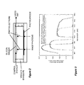
- Fig. 1 shows the relative nighttime photon flux versus wavelength on moonlit and moonless nights as measured by Vatsia over the 0.47 to 1.93 micron spectral range.
- the variation in available light at particular wavelength bands is due to atmospheric absorption over specific regions due to water and other atmospheric gases and due to the emission spectrum of optical sources at night including moonlight, starlight, and emission from the upper atmosphere.
- thermal radiation due to blackbody emission of objects at ambient temperature becomes significant relative to other sources of available light at night and one moves into the realm of thermal imaging.
- the object of this invention is to provide improved night time imaging performance using reflected ambient light, not thermal imaging using blackbody radiation.
- Fig. 1 shows that substantially more light is available on moonless nights at longer wavelengths.
- the low amount of light available on moonless nights provides the greatest challenge to Night Vision image sensors.
- Night Vision device performance is limited by the amount of available light on moonless nights. Due to the increased photon flux at wavelengths above 1.5 ⁇ m, designers of night vision image sensors have focused on developing sensors that extend sensitivity to these higher wavelengths, i.e., to include detection of photons in the 1.4 - 1.9 ⁇ m range. An example of this is disclosed in U.S.
- Patent 7,608,825 B2 where the long wavelength cutoff of the semiconductor optical absorber layer is extended from 1.7 ⁇ m for In 0.53 Ga 0.47 As to wavelengths as long at 3.0 ⁇ m by epitaxial growth of GaInNAsP, GaInNAsSb or GaInNAs semiconductor layers of varying composition of the Group III and Group V constituents of the quaternary or quinary semiconductor lattice matched to an InP substrate.
- High performance sensors have other requirements for good night vision performance in addition to spectral response range.
- Two fundamental requirements are high quantum efficiency (photon detection efficiency) over the sensitive wavelength range with low associated dark noise. Dark noise is dominated by thermally generated dark current in a high performance sensor. Dark current magnitude is a critical performance parameter as fundamentally the dark noise associated with the dark current needs to be less than the photogenerated current to obtain imaging performance at a given light level.
- the combination of these requirements on the photosensing element limits the choice of semiconductor materials for the photocathode or photodiode and specifies image sensor operating temperature.
- InGaAs lattice matched to an InP substrate has been used in the past to meet these requirements for the photosensing material.
- the InGaAs composition that results in the same lattice constant as InP is In 0.53 Ga 0.47
- this composition of InGaAs is also denoted by the term "lattice matched InGaAs or InGaAs lattice matched to InP" in this disclosure.
- InGaAs lattice matched to InP is sensitive to 1.7 micron and shorter wavelength light. The short wavelength cutoff ranges from 0.4 to 0.95 micron depending upon the specific structure of the photocathode or photodiode.
- This wavelength range captures substantially more light than the commonly used GaAs, Generation-III, photocathode that is sensitive over the 0.4 - 0.9 micron Visible Near Infra-Red (VNIR) wavelength band.
- VNIR Visible Near Infra-Red
- System size, weight, unit cost, and power consumption are critical night vision system metrics. Size and performance are impacted by the relatively large pixel size (15 ⁇ m for state-of-the-art, developmental, FPAs and 25 ⁇ m for commercially available product) of the available SWIR FPAs.
- the minimum pixel size is limited by the bump bonding technology used to attach the photodiode array to the ROIC. This restricts overall sensor format to SXGA (1280 x 1024) and lower array sizes to maintain an acceptable overall FPA size. Larger FPAs would increase system size and cost to unacceptable levels for manportable applications.
- a typical image intensifier tube based night vision goggle has a 40° Field of View and the equivalent resolution of a modem image intensifier is approximately 6 to 9 megapixels.
- One object of this invention is to increase the array size of a SWIR image sensor relative to the prior art for use as a night vision image sensor.
- Cooling is required as the level of dark current emitted by either an In 1-x Ga x As or other semiconductor used for imaging in the SWIR band or at longer wavelengths is too high at room temperature (20° - 25°C) to enable low light level imaging on moonless nights.
- the provision of cooling for portable applications places a high demand on batteries, thereby reducing the useful operational time of the device before batteries are emptied.
- a SWIR EBCCD can be achieved by replacing the GaAs photocathode with an In 0.53 Ga 0.47 As based photocathode. This has been demonstrated by Intevac for Laser Illuminated Viewing and Ranging (LIV AR ® ) applications ( V. Aebi and P. Vallianos, "Laser-illuminated viewing provides long-range detail," LASER FOCUS WORLD, September 2000 ). These applications utilize a pulsed eyesafe laser illuminator typically operating at 1.57 ⁇ m.
- the present LIVAR camera utilizes an InGaAs photocathode used in an EBAPS with a CMOS anode array.
- the photocathode is gated on for very short periods (typically in the 100 ns to 2 ⁇ s time range).
- This low duty cycle enables operation at ambient temperature ( ⁇ 40 degrees C) without performance being photocathode dark current limited.
- InGaAs lattice matched to InP and used in a TE photocathode configuration is a good choice for this application with 20 degree C emitted dark current in the 10 - 40 nA/cm 2 range and good sensitivity in the 1.5 - 1.6 micron spectral range for compatibility with eyesafe laser illuminators.
- Passive night time imaging requires continuous integration of the light by the image sensor to maximize light collection. Under these conditions substantial cooling is required of the In 0.53 Ga 0.47 As TE photocathode to reduce dark current to an acceptable level to achieve signal limited performance at night (typically cooling to -40 degrees C is required). This level of cooling substantial increases system size and power requirements making the approach unsuitable for battery operated night vision applications.
- focal plane arrays used for night vision applications also require cooling to reduce focal plane dark current to levels where it does not limit performance on moonless nights.
- the smaller bandgap semiconductors such as InSb or various alloys of Hg 1-x Cd x Te also require cooling to temperatures substantially below 20°C to reduce dark current.
- US 2008/0142714 teaches an image pickup device which picks up an image of an object by absorbing light in a near infrared region reflected from the object and which has semiconductor photodetectors including an absorption layer of a bandgap wavelength in the range of 1.65 to 3.0 ⁇ m.
- the image pickup device picks up an image of an object by absorbing light in a near infrared region reflected from the object.
- This image pickup device comprises semiconductor photodetectors which includes an absorption layer having a bandgap wavelength in the range of 1.65 to 3.0 ⁇ m.
- US 6,740,851 B2 discloses a photodetector including a semiconductor conductive layer, light-absorbing layer and wide bandgap layer, which are stacked in this order on a semi-insulating semiconductor substrate.
- the conductive layer has been formed on a surface region of the substrate.
- the photodetector further includes a doped region defined in part of the wide bandgap layer.
- the conductive layer has etch susceptibility different from that of the substrate.
- the photodetector comprises a semi-insulating semiconductor substrate; a semiconductor conductive layer, which has been formed on a surface region of the substrate and has electrical conductivity; a light-absorbing layer, which has been formed on the conductive layer and absorbs light that has been incident on the photodetector; a wide bandgap layer, which has been formed on the light-absorbing layer and has a bandgap wider than a bandgap of the light-absorbing layer; and a doped region, which has been defined in the wide bandgap layer by doping part of the wide bandgap layer with a dopant that reaches the light-absorbing layer, wherein the conductive layer has etch susceptibility different from that of the substrate.
- the substrate is made of InP
- the conductive layer is made of InGaAsP
- the light-absorbing layer is made of InGaAs
- the wide bandgap layer is made of InP.
- EP 1 796 169 A1 discloses a photo-detector, in which metal wiring for connecting electrodes is arranged on a planarized surface and thus the metal wiring arrangement is simplified, and a method of manufacturing the same are provided.
- the photo-detector includes a multi-layer compound semiconductor layer formed on a compound semiconductor substrate. A number of p-n junction diodes are arranged in a regular order in a selected region of the compound semiconductor layer, and an isolation region for individually isolating the p-n junction diodes is formed by implanting impurity ions in the multi-layer compound semiconductor layer. The isolation region and the surface of the compound semiconductor layer are positioned on the same level.
- the isolation region may be a Fe-impurity region.
- the device for generating an electrical signal in response to light comprises a photodetector including at least one superlattice layer operative to generate an electrical signal in response to light incident thereon; and one or more lenslets for directing light onto the photodetector.
- the photodetector incudes one or more photosensitive pixels, each of the pixels having a superlattice layer, a non-intentionally-doped (NID) superlattice layer, and a contact layer and wherein the active area of each of the pixels is smaller than the projection area of each of the lenslets.
- NID non-intentionally-doped
- CMOS imager including passive pixel sensors which in tum generates an electronic image which is fed out of the vacuum and is used to create useful images corresponding to the low level input image. Also a camera and other low light imaging devices are described.
- the method to record low light level images comprises projecting an input image to be recorded onto a photocathode to cause said photocathode to release electrons in a spatial configuration into a vacuum chamber conforming to the input image, positioning a passive pixel sensor at a receiving plane of the electron image within the vacuum chamber, creating a electron driving field from the photocathode to the passive pixel sensor to cause electrons to bombard the passive pixel sensor within the vacuum chamber, and directing the output of said active pixel sensor out of said vacuum chamber.
- the night vision apparatus comprises the features of claim 1, Preferred embodiments of the invention are characterized in the dependent claims.
- the sensor for a night vision camera comprises a semiconductor absorption layer of composition that limits long wavelength response cutoff to between 1.25 to 1.4 ⁇ m wavelength.
- a semiconductor absorption layer of composition that limits long wavelength response cutoff to between 1.25 to 1.4 ⁇ m wavelength.
- this choice seems counter-intuitive, as conventionally artisans seeks to have sensors having the highest possible long wavelength response cutoff in order to absorb as much light as possible. Therefore, artisans seeks sensors having absorption layer that absorbs light beyond 1.7 ⁇ m, so as to absorb the light available beyond the deep reduction in available light in the 1.4 ⁇ m - 1.5 ⁇ m wavelength range, as shown in Fig. 1 .
- the inventor has found that for portable applications, the reduced dark current of a sensor having long wavelength response cutoff to between 1.25 to 1.4 ⁇ m, provides advantages that more than compensate for the loss of light detection at wavelengths above 1.4 ⁇ m. These advantages will be discussed below.
- the apparatus senses light at low lighting conditions at wavelengths below 1.4 ⁇ m with low dark current at ambient operating temperatures, energy consumption is reduced, as the sensor does not require active cooling.
- a photocathode, photodiode, or avalanche photodiode array is optimized for use in mobile Night Vision systems for use in the Short Wave Infra-Red (SWIR) 0.9 ⁇ m - 2.0 ⁇ m wavelength band.
- SWIR Short Wave Infra-Red
- a novel semiconductor structure for the photocathode or photodiode array is optimized to achieve improved performance at elevated operating temperatures relative to prior art SWIR image sensors.
- the novel structure is suitable for use in image intensifiers for direct view Night Vision systems, photocathode based cameras, and in semiconductor focal plane based image sensors and cameras based on solid state photodiode or avalanche photodiode arrays.
- Photocathode or photodiode dark current and overall camera power consumption are addressed through use Of In 1-x Ga x As y P 1-y lattice matched to InP for the SWIR photocathode or photodiode array.
- the In 1-x Ga x As y P 1-y composition is optimized to obtain a lattice constant matched to the InP lattice constant.
- E g,dir is in eV and y is the As compositional value as defined in the preceding equations for lattice matching to InP.
- E g,dir is defined by the above equation at a temperature of 298°K.
- the In 1-x Ga x As y P 1-y composition is chosen to optimize spectral response of the In 1-x Ga x As y P 1-y to maximize detection of moonless night sky illumination while minimizing dark current generated in the In 1-x Ga x As y P 1-y absorber layer.
- Fig. 1 shows the spectral intensity of the night sky illumination as a function of wavelength. This data is disclosed by Vatsia, Mirshri, L. "Atmospheric Optical Environment", Research and Development Technical Report ECOM-7023, September (1972 ). Curve 1 on this graph plots the illumination level versus wavelength on a moonless night. This represents the darkest, most challenging, condition for operation of a night vision device. It can be observed that there is a large reduction in the available light at night in the 1.4 to 1.5 ⁇ m wavelength range. This reduction is caused by absorption of optical radiation in this band by water in the atmosphere. On the other hand, there is a second "maxima" beyond 1.4 ⁇ m, centered at about 1.63 ⁇ m.
- an absorption layer of In 1-x Ga x As y P 1-y is designed to have a 1.4 ⁇ m cutoff wavelength.
- the specific composition that results in a 1.4 ⁇ m cutoff wavelength is: In 0.68 Ga 0.32 As 0.69 P 0.31 -
- One example is the (Al s Ga 1-s ) 1-t In t As semiconductor alloy system where s, 1, and t all can vary between 0 and 1.
- This system also has a range of compositions that are lattice matched to an InP substrate and can be used to limit the long wavelength cutoff of the semiconductor layer to the 1.25 ⁇ m to 1.4 ⁇ m range as specified here-in and with the same advantage of reduced dark current generation as the In 1-x Ga x As y P 1-y InP lattice matched system.
- the spectral coverage of this material is from 950 -1400 nm (termed Near SWIR or NSWIR) it has the advantage of a factor of 100 or more reduced dark current relative to a conventional InGaAs photocathode or photodiode array operated at the same temperature, thereby greatly reducing sensor cooling requirements.
- This spectral band still has a factor of 5 or greater photon flux relative to the GaAs VNIR band and is compatible with commonly available 1.3 ⁇ m laser or LED sources for out of band laser pointers, illuminators, and markers.
- the long wavelength cutoff of the InGaAsP photocathode was chosen in the 1250 -1400 nm range (In 1-x Ga x As y P 1-y compositions in the range of In 0.68 Ga 0.32 As 0.69 P 0.31 to In 0.76 Ga 0.24 As 0.51 P 0.49 as defined by the above equations for lattice match to InP) to enable good detection of the peak in illumination intensity on moonless nights centered at approximately 1280 nm ( Fig. 1 ).
- the camera has a 1600 x 1200 format with a 10.8 ⁇ m pixel and operates at 60 Hz frame rate.
- An aspect of the invention is to greatly extend the state-of-the-art of FPAs operating in the SWIR spectral band.
- the sensor will extend sensitivity to near single photon level and reduce pixel size to 10.8 ⁇ m for an UXGA array (1600 x 1200 format, 2 megapixel array).
- the FPA achieves this performance by combining a backside illuminated 2 megapixel Active Pixel Sensor (APS) CMOS image chip in an electron bombarded (EB) mode with an InGaAsP based Transferred Electron (TE) photocathode with > 30% QE in the NSWIR spectral band.
- APS Active Pixel Sensor
- EB electron bombarded
- TE Transferred Electron
- This TE photocathode based Electron Bombarded Active Pixel Sensor allows extreme low light sensitivity (single photon sensitivity) for increased sensitivity over present SWIR cameras (InGaAs focal plane array) combined with higher resolution.
- the NSWIR EBAPS is compatible with low power, battery operated, cameras due to reduced cooling requirements and use of a low power APS CMOS image chip.
- CMOS image chip that forms the anode of the sensor ( Fig. 2 ).
- Low noise gain is achieved by electron multiplication resulting when the high velocity electron beam dissipates its energy in the silicon of the imager chip to produce electron-hole pairs by the electron-bombarded semiconductor gain process.
- the low read out noise of the CMOS chip when combined with the high electron bombarded gain results in an effective noise floor referenced to the photocathode of well under 1 photoelectron for close to single photon sensitivity.
- EBAPS technology enables the spectral response of the image sensor to be modified by changing the photocathode. This enables re-use of the CMOS readout array and camera electronics.
- Fig. 3 illustrates quantum efficiency curves for III-V semiconductor photocathodes fabricated by Intevac.
- the performance of staring (passive) SWIR sensors operated at ambient temperature is typically dark current limited at low light levels.
- the sensor becomes dark current limited when the number of photoelectrons collected by the pixel per integration time generated by the input photon flux falls below the square root of the number of dark current electrons generated in the same integration time in the pixel.
- the image sensor becomes dark current limited at a higher input signal level due to non-uniformity of the dark current generation in the image sensor and with the inclusion of the signal shot noise as part of the noise term in the signal-to-noise of the pixel.
- the In 0.53 Ga 0.47 As TE photocathode EBAPS is operated at ambient temperature (>20°C) for LIVAR and becomes dark current limited when operated as a passive image sensor under night time illumination conditions. This is also the case for present In 0.53 Ga 0.47 As photodiode array FPAs.
- the present In 0.53 Ga 0.47 As TE photocathode EBAPS camera requires several other improvements to allow application of EBAPS based cameras for passive night vision imaging in the SWIR band.
- the improvements provided by embodiments of the invention may include:
- the first three improvements can be obtained by fabricating an EBAPS anode EBAPS using a CMOS anode array with a larger format.
- this array is UXGA format (1600 x 1200 pixels) with a 10.8 micron pixel pitch resulting in a 4/" optical format for the image sensor.
- Response in the SWIR wavelength band can be obtained by using an InGaAs TE photocathode.
- the fourth improvement can be obtained by limiting the long wavelength cutoff of the TE photocathode to approximately 1.35 ⁇ m ( Fig. 3 InGaAsP photocathode spectral response for InGaAsP with a composition of In 0.71 Ga 0.29 As 0.63 P 0.37 ).
- the disadvantage of this approach is a reduction in the available light on moonless nights relative to the spectral response of the InGaAs photocathode shown in Fig. 3 .
- the Table 1 shows the relative nighttime photon flux versus wavelength band on a moonless night as measured by Vatsia ( Fig. 1 ).
- the short wavelength cut-off for NSWIR and SWIR detectors is often chosen to be 950 nm.
- the NSWIR sensor may show further benefits relative to an In 0.53 Ga 0.47 As SWIR FPA due to the contrast reversal at about 1400 nm with a green foliage background.
- Green foliage is highly reflective from approximately 700 nm to 1370 nm with lower reflectivity outside this band. Contrast of many objects or targets of interest relative to a green foliage background may be enhanced by a NSWIR spectral response where the focal plane is only sensitive within this spectral band relative to a sensor with a SWIR spectral response.
- Night Vision performance has been modeled comparing the NSWIR In 0.71 Ga 0.29 As 0.63 P 0.37 photocathode with an image sensor utilizing an In 0.53 Ga 0.47 As photocathode lattice matched to InP. Performance was compared under the darkest conditions reported by Vatsia in Fig. 1 , Night Glow only.
- the modeling assumed a 30% reflective target across the specified spectral band and use of a T/1.4 lens and a 30 frame per second imaging sensor with an integration time of 1/30 second.
- SNR was calculated over a 0.2 mm spot size as is the case for image intensifyers used in night vision goggles. This approach takes into account the ability of eye/brain of the observer to integrate low SNR imagery both temporally and spatially.
- the modeling shows that the additional light over the SWIR band results in approximately a factor of two greater signal.
- the higher signal is more than offset at a 20 degree C operating temperature by the much higher dark current of the InGaAs photocathode relative to the InGaAsP photocathode.
- the InGaAsP photocathode device has a factor of 5 greater SNR than the InGaAs photocathode device.
- FIG. 4 An uncorrected (Nonuniformity Correction not applied) daytime image captured with the NSWIR EBAPS camera is shown in Fig. 4 .
- This image was captured during the day using a f/1.4, 25 mm focal length, lens optimized for the SWIR band.
- the high voltage gate time for this image was 1 ⁇ s to avoid image saturation. This indicates that the camera has high sensitivity as the integration time can be increased by about 5 orders of magnitude for video rate nighttime imaging.
- the image gives an example of NSWIR imagery.
- the high reflectivity of green foliage in the NSWIR band is also evident in the image. This demonstrates the good image contrast obtained in the NSWIR spectral band relative to foliage.
- the EBAPS NSWIR camera according to embodiments of the invention will significantly outperform (low light sensitivity and power) present solid-state and photocathode based InGaAs image sensor cameras.
- Table 4 summarizes the performance for one embodiment of the new camera. Table 4: Performance for NSWIR EBAPS NSWIR EBAPS Focal Plane Format UXGA (1600 x 1200 pixels) Pixel Size 10.8 ⁇ m Frame Rate 60 fps Effective Read Noise ⁇ 1 electron Spectral Response 950 - 1350 nm Quantum Efficiency > 30% Dark Current @ 20°C ⁇ 100 pA/cm 2
- the invention benefits and improvements are the reduced room temperature dark current for low power operation combined with the low effective readout noise enabled by the high electron bombarded gain in the EBAPS.
- the other features are the small pixel size and the UXGA format.
- the UXGA format substantially improves resolution at all light levels allowing longer recognition ranges.
- the small pixel size enables small optics for a given field of view. Small optics are critical to meet size and weight objectives for man-portable equipment.
- FIG. 5 A structure for an embodiment of a NSWIR TE photocathode is shown in Fig. 5 .
- An InP substrate 500 is coated on its front surface (light receiving surface) with an anti-reflective coating ARC 505.
- An InP buffer layer is formed on the back side of the substrate 500.
- an absorption layer 515 is fabricated on the buffer layer.
- an In 0.71 Ga 0.29 As 0.63 P 0.37 layer is used as the photon absorbing layer.
- the composition of this semiconductor (lattice matched to InP) is chosen to select the desired long wavelength cutoff for the photocathode. In this case the bandgap is chosen in the 1.35 - 1.40 microns wavelength.
- a grading layer 520 is fabricated on the absorber, and InP emitted layer 525 is fabricated on the grading layer.
- a Schottky barrier 530 caps the back of the sensor and grid lines 535 are provided to allow a bias voltage to be applied to the Schottky barrier.
- the InGaAsP bandedge is chosen to fall in the 1.35 - 1.4 micron range as there is a reduction in night sky illumination in the 1.4 -1.5 micron range as shown by Vatsia. Sensitivity in the 1.4 to 1.5 micron range would not significantly increase the number of detected photons under night time illumination conditions.
- an SXGA format CMOS based EBAPS is fabricated utilizing a NSWIR InGaAsP TE photocathode with a spectral response from 950 - 1350 nm.
- a Camera utilizing the NSWIR EBAPS sensor can be fabricated.
- the camera may be supplied with a Thermo Electric Cooler (TEC) controller to enable up to 20°C lower operating temperature than ambient and allow performance investigation at below ambient operating temperatures.
- TEC Thermo Electric Cooler
- the camera will utilize a cameralink video interface.
- the camera can be integrated with standard lens.
- a PIN photodiode structure according to this example is shown in Fig. 6 .
- An array of photodiodes with this or similar structures familiar to those skilled in the art can be hybridized with a ROIC to form a NSWIR image sensor according to this invention.
- An InP buffer layer 605 is fabricated over an InP substrate 600 of n+ type.
- an InGaAsP active layer 610 is fabricated over the buffer layer.
- the InGaAsP layer is an n-type layer having a 1.4 ⁇ m cutoff wavelength. For example, a 3 micron thick layer of In 0.71 Ga 0.29 As 0.63 P 0.37 can be used.
- An InP cap layer 615 is fabricated over the active layer 610, and a p + -type diffused layer 620 is formed through the cap, partially extending (in this example, 0.25 microns) into the active layer 610.
- the active pixel sensor component includes a vacuum enclosure 3 that houses a photocathode 12 in proximity focus with a specialized active pixel array sensor chip 13.
- the sensor chip 13 forms the anode for receiving proximity focused photoelectrons from the photocathode 12.
- the active pixel array sensor 13 is mounted with its backside facing the photocathode 12.
- the backside of the substrate of the active pixel array sensor 13 is thinned. Thinning the backside of the substrate provides for a greater collection efficiency of the photoelectron excited carriers and reduces the crosstalk between pixels as a result of diffusion.
- the active pixel sensor array 13 may also include a passivated surface or layer.
- the base of the vacuum device 3 is a transparent faceplate 21.
- the photocathode 12 is positioned on the faceplate 21.
- Vacuum enclosure sidewalls 22 extend between the transparent faceplate 21 and the header assembly 23.
- the active pixel sensor chip 13 is positioned on the header assembly 23.
- the header assembly 23 also allows for electrical feedthroughs for applying and reading back control voltages 17, bias voltage 18, and signal output lines 20 associated with the active pixel array sensor chip 13. Control electronics (not shown) are used to read out and operate the pixel array.
- the photocathode 12 is an InP/InGaAsP transferred electron photocathode.
- a photocathode bias voltage is applied between the grid line ( Fig. 5 ) and the InP substrate to bias the photocathode and enable photoemission. See, for example, US Patent No. 5,047,821 , the entirety of which is hereby incorporated by reference.
- An electron accelerating voltage 37 is applied to the photocathode 12 relative to the active pixel sensor chip 13.
- Photoelectrons 15 are emitted from the photocathode 12 in response to incident light in the form of an optical image 9.
- Optical components (not shown) are typically employed to form the optical image on the photocathode 12.
- a projection system may be used to place the image on the photocathode 12.
- An anode voltage 18 is applied to the sensor 13.
- the photoelectrons 15 are accelerated by virtue of the difference between the accelerating voltage 37 and the anode voltage 18.
- the accelerating voltage 37 is negative with respect to the anode voltage 18. This permits biasing the sensor 13 to near (or at) ground potential to simplify interfacing with other components.
- Control signals and bias voltages 17 are applied to the active pixel sensor 3 and a video output signal 20 may be taken off the sensor 13.
- the electron bombarded active pixel array sensor 13 is usefully employed in various systems, such as cameras, night vision imagers and the like. To that end, optical lenses or the like form an image of real objects on a focal plane which is disposed to coincide with the photocathode 12. Taken together, the electron bombarded active pixel array component with optics, power supply and control electronics may be regarded as a camera system.
Landscapes
- Solid State Image Pick-Up Elements (AREA)
- Transforming Light Signals Into Electric Signals (AREA)
- Image-Pickup Tubes, Image-Amplification Tubes, And Storage Tubes (AREA)
- Light Receiving Elements (AREA)
Priority Applications (1)
| Application Number | Priority Date | Filing Date | Title |
|---|---|---|---|
| EP14191472.1A EP2835830B1 (en) | 2009-08-31 | 2010-08-31 | Night-vision sensor and apparatus |
Applications Claiming Priority (2)
| Application Number | Priority Date | Filing Date | Title |
|---|---|---|---|
| US23864109P | 2009-08-31 | 2009-08-31 | |
| PCT/US2010/047406 WO2011026143A1 (en) | 2009-08-31 | 2010-08-31 | Low energy portable low-light camera with wavelength cutoff |
Related Child Applications (1)
| Application Number | Title | Priority Date | Filing Date |
|---|---|---|---|
| EP14191472.1A Division EP2835830B1 (en) | 2009-08-31 | 2010-08-31 | Night-vision sensor and apparatus |
Publications (3)
| Publication Number | Publication Date |
|---|---|
| EP2474034A1 EP2474034A1 (en) | 2012-07-11 |
| EP2474034A4 EP2474034A4 (en) | 2014-02-26 |
| EP2474034B1 true EP2474034B1 (en) | 2014-11-12 |
Family
ID=43623431
Family Applications (2)
| Application Number | Title | Priority Date | Filing Date |
|---|---|---|---|
| EP10812779.6A Active EP2474034B1 (en) | 2009-08-31 | 2010-08-31 | Low energy portable low-light camera with wavelength cutoff |
| EP14191472.1A Active EP2835830B1 (en) | 2009-08-31 | 2010-08-31 | Night-vision sensor and apparatus |
Family Applications After (1)
| Application Number | Title | Priority Date | Filing Date |
|---|---|---|---|
| EP14191472.1A Active EP2835830B1 (en) | 2009-08-31 | 2010-08-31 | Night-vision sensor and apparatus |
Country Status (7)
Cited By (1)
| Publication number | Priority date | Publication date | Assignee | Title |
|---|---|---|---|---|
| EP4189719A4 (en) * | 2020-07-29 | 2024-07-24 | Elbit Systems of America, LLC | Wafer scale enhanced gain electron bombarded cmos imager |
Families Citing this family (10)
| Publication number | Priority date | Publication date | Assignee | Title |
|---|---|---|---|---|
| US8581228B2 (en) * | 2009-01-22 | 2013-11-12 | Bae Systems Information And Electronic Systems Integration Inc. | Corner cube enhanced photocathode |
| US8692198B2 (en) * | 2010-04-21 | 2014-04-08 | Sionyx, Inc. | Photosensitive imaging devices and associated methods |
| US8687110B1 (en) * | 2011-05-31 | 2014-04-01 | Flir Systems, Inc. | Intelligent power management for actively-cooled cameras |
| DE102017215715B4 (de) * | 2017-09-06 | 2019-09-12 | Fraunhofer-Gesellschaft zur Förderung der angewandten Forschung e.V. | Optischer bildaufnehmer zur aufnahme zweidimensionaler bilder im nahen infrarotbereich |
| US11606515B2 (en) | 2019-10-24 | 2023-03-14 | Trieye Ltd | Methods and systems for active SWIR imaging using germanium receivers |
| US11665447B2 (en) | 2019-10-24 | 2023-05-30 | Trieye Ltd. | Systems and methods for compensating for dark current in a photodetecting device |
| US11811194B2 (en) | 2019-10-24 | 2023-11-07 | Trieye Ltd. | Passive Q-switched lasers and methods for operation and manufacture thereof |
| US11810990B2 (en) | 2019-10-24 | 2023-11-07 | Trieye Ltd. | Electro-optical systems, methods and computer program products for image generation |
| EP3891525B1 (en) * | 2019-10-24 | 2022-05-11 | Trieye Ltd. | Photonics systems and methods |
| US11551906B1 (en) * | 2021-06-30 | 2023-01-10 | Fei Company | Time-gated detection, dual-layer SPAD-based electron detection |
Family Cites Families (22)
| Publication number | Priority date | Publication date | Assignee | Title |
|---|---|---|---|---|
| FR2574239B1 (fr) | 1984-11-30 | 1987-01-23 | Labo Electronique Physique | Capteur d'images pour camera fonctionnant en mode " jour-nuit " |
| US5047821A (en) * | 1990-03-15 | 1991-09-10 | Intevac, Inc. | Transferred electron III-V semiconductor photocathode |
| US5576559A (en) * | 1994-11-01 | 1996-11-19 | Intevac, Inc. | Heterojunction electron transfer device |
| EP0773591A3 (en) * | 1995-11-13 | 1998-09-16 | Sumitomo Electric Industries, Ltd. | Light emitting/detecting module |
| US6121612A (en) | 1997-10-22 | 2000-09-19 | Litton Systems, Inc. | Night vision device, image intensifier and photomultiplier tube, transfer-electron photocathode for such, and method of making |
| US6229152B1 (en) | 1999-02-18 | 2001-05-08 | The Trustees Of Princeton University | Strain compensated indium galium arsenide quantum well photoconductors with high indium content extended wavelength operation |
| US6573581B1 (en) | 1999-03-01 | 2003-06-03 | Finisar Corporation | Reduced dark current pin photo diodes using intentional doping |
| US6657178B2 (en) * | 1999-07-20 | 2003-12-02 | Intevac, Inc. | Electron bombarded passive pixel sensor imaging |
| US6285018B1 (en) | 1999-07-20 | 2001-09-04 | Intevac, Inc. | Electron bombarded active pixel sensor |
| JP2002050786A (ja) * | 2000-05-25 | 2002-02-15 | Matsushita Electric Ind Co Ltd | 受光素子およびその製造方法 |
| US6586718B2 (en) * | 2000-05-25 | 2003-07-01 | Matsushita Electric Industrial Co., Ltd. | Photodetector and method for fabricating the same |
| US6597112B1 (en) | 2000-08-10 | 2003-07-22 | Itt Manufacturing Enterprises, Inc. | Photocathode for night vision image intensifier and method of manufacture |
| JP2002289904A (ja) | 2001-03-23 | 2002-10-04 | Sumitomo Electric Ind Ltd | 半導体受光素子とその製造方法 |
| US7276749B2 (en) | 2002-02-05 | 2007-10-02 | E-Phocus, Inc. | Image sensor with microcrystalline germanium photodiode layer |
| US6852976B2 (en) | 2002-09-26 | 2005-02-08 | Indigo Systems Corporation | Infrared detector array with improved spectral range and method for making the same |
| US7453129B2 (en) | 2002-12-18 | 2008-11-18 | Noble Peak Vision Corp. | Image sensor comprising isolated germanium photodetectors integrated with a silicon substrate and silicon circuitry |
| KR100670828B1 (ko) * | 2005-12-12 | 2007-01-19 | 한국전자통신연구원 | 적외선 레이저 레이다의 영상 신호를 검출하기 위한 광검출기 및 그 제조방법 |
| JP2007201432A (ja) * | 2005-12-28 | 2007-08-09 | Sumitomo Electric Ind Ltd | 撮像装置、視界支援装置、暗視装置、航海支援装置および監視装置 |
| US7651880B2 (en) | 2006-11-04 | 2010-01-26 | Sharp Laboratories Of America, Inc. | Ge short wavelength infrared imager |
| US7608825B2 (en) * | 2006-12-14 | 2009-10-27 | Sumitomo Electric Industries, Ltd. | Image pickup device, vision enhancement apparatus, night-vision apparatus, navigation support apparatus, and monitoring apparatus |
| US7598582B2 (en) | 2007-06-13 | 2009-10-06 | The Boeing Company | Ultra low dark current pin photodetector |
| US20090020700A1 (en) * | 2007-07-17 | 2009-01-22 | Locheed Martin Corporation | Method and device for generating an electrical signal in response to light |
-
2010
- 2010-08-31 JP JP2012527110A patent/JP5628315B2/ja not_active Expired - Fee Related
- 2010-08-31 CA CA2772394A patent/CA2772394C/en active Active
- 2010-08-31 EP EP10812779.6A patent/EP2474034B1/en active Active
- 2010-08-31 EP EP14191472.1A patent/EP2835830B1/en active Active
- 2010-08-31 US US12/873,225 patent/US8421012B2/en active Active
- 2010-08-31 AU AU2010286372A patent/AU2010286372B2/en active Active
- 2010-08-31 WO PCT/US2010/047406 patent/WO2011026143A1/en active Application Filing
-
2012
- 2012-02-28 IL IL218363A patent/IL218363A0/en active IP Right Grant
Cited By (1)
| Publication number | Priority date | Publication date | Assignee | Title |
|---|---|---|---|---|
| EP4189719A4 (en) * | 2020-07-29 | 2024-07-24 | Elbit Systems of America, LLC | Wafer scale enhanced gain electron bombarded cmos imager |
Also Published As
| Publication number | Publication date |
|---|---|
| EP2835830A2 (en) | 2015-02-11 |
| EP2835830A3 (en) | 2015-05-20 |
| JP5628315B2 (ja) | 2014-11-19 |
| JP2013503455A (ja) | 2013-01-31 |
| AU2010286372B2 (en) | 2014-09-18 |
| WO2011026143A1 (en) | 2011-03-03 |
| US20110049365A1 (en) | 2011-03-03 |
| EP2474034A1 (en) | 2012-07-11 |
| EP2474034A4 (en) | 2014-02-26 |
| EP2835830B1 (en) | 2018-10-17 |
| CA2772394C (en) | 2018-02-06 |
| AU2010286372A1 (en) | 2012-03-22 |
| CA2772394A1 (en) | 2011-03-03 |
| US8421012B2 (en) | 2013-04-16 |
| IL218363A0 (en) | 2012-04-30 |
Similar Documents
| Publication | Publication Date | Title |
|---|---|---|
| EP2474034B1 (en) | Low energy portable low-light camera with wavelength cutoff | |
| CA2379956C (en) | Electron bombarded active pixel sensor | |
| US6657178B2 (en) | Electron bombarded passive pixel sensor imaging | |
| US5818052A (en) | Low light level solid state image sensor | |
| EP1891678B1 (en) | Photocathode structure and operation | |
| US20100327387A1 (en) | Avalanche Photodiode | |
| Martin et al. | 640x512 InGaAs focal plane array camera for visible and SWIR imaging | |
| Delaunay et al. | Background limited performance of long wavelength infrared focal plane arrays fabricated from M-structure InAs–GaSb superlattices | |
| Rouvié et al. | InGaAs focal plane array developments at III-V Lab | |
| JP2004510352A (ja) | 室温で動作する高性能紫外線イメジャ | |
| US20230041955A1 (en) | Sensor with upconversion layer | |
| Martin et al. | 320x240 pixel InGaAs/InP focal plane array for short-wave infrared and visible light imaging | |
| Turner et al. | The development of, and applications for, extended response (0.7 to 1.7 µm) InGaAs focal plane arrays | |
| US20250076108A1 (en) | High-Definition Broad-Band Visible-shortwave Infrared (SWIR) Sensors for Laser Detection | |
| EP1652237B1 (en) | Backside thinning of image array devices | |
| JP2009027047A (ja) | 検出装置 | |
| JP2024159599A (ja) | 低照度性能改善のための、集光器及びフルデプスディープアイソレーショントレンチを有する光学ピクセル | |
| Brennan | A. SOLID-STATE ALTERNATIVES FOR IMAGE INTENSIFICATION | |
| Cohen et al. | An Indium Gallium Arsenide Visible/SWIR Focal Plane Array for Low Light Level Imaging | |
| Inebund et al. | New photocathodes for UV and IR spectral range for prospective photodetectors |
Legal Events
| Date | Code | Title | Description |
|---|---|---|---|
| PUAI | Public reference made under article 153(3) epc to a published international application that has entered the european phase |
Free format text: ORIGINAL CODE: 0009012 |
|
| 17P | Request for examination filed |
Effective date: 20120302 |
|
| AK | Designated contracting states |
Kind code of ref document: A1 Designated state(s): AL AT BE BG CH CY CZ DE DK EE ES FI FR GB GR HR HU IE IS IT LI LT LU LV MC MK MT NL NO PL PT RO SE SI SK SM TR |
|
| DAX | Request for extension of the european patent (deleted) | ||
| A4 | Supplementary search report drawn up and despatched |
Effective date: 20140123 |
|
| RIC1 | Information provided on ipc code assigned before grant |
Ipc: H01L 31/109 20060101ALI20140117BHEP Ipc: H01L 31/0304 20060101ALI20140117BHEP Ipc: H01L 27/146 20060101AFI20140117BHEP |
|
| GRAP | Despatch of communication of intention to grant a patent |
Free format text: ORIGINAL CODE: EPIDOSNIGR1 |
|
| INTG | Intention to grant announced |
Effective date: 20140625 |
|
| GRAS | Grant fee paid |
Free format text: ORIGINAL CODE: EPIDOSNIGR3 |
|
| GRAA | (expected) grant |
Free format text: ORIGINAL CODE: 0009210 |
|
| AK | Designated contracting states |
Kind code of ref document: B1 Designated state(s): AL AT BE BG CH CY CZ DE DK EE ES FI FR GB GR HR HU IE IS IT LI LT LU LV MC MK MT NL NO PL PT RO SE SI SK SM TR |
|
| REG | Reference to a national code |
Ref country code: GB Ref legal event code: FG4D |
|
| REG | Reference to a national code |
Ref country code: CH Ref legal event code: EP |
|
| REG | Reference to a national code |
Ref country code: AT Ref legal event code: REF Ref document number: 696208 Country of ref document: AT Kind code of ref document: T Effective date: 20141115 |
|
| REG | Reference to a national code |
Ref country code: IE Ref legal event code: FG4D |
|
| REG | Reference to a national code |
Ref country code: DE Ref legal event code: R096 Ref document number: 602010020254 Country of ref document: DE Effective date: 20141224 |
|
| REG | Reference to a national code |
Ref country code: SE Ref legal event code: TRGR |
|
| REG | Reference to a national code |
Ref country code: NL Ref legal event code: T3 |
|
| REG | Reference to a national code |
Ref country code: AT Ref legal event code: MK05 Ref document number: 696208 Country of ref document: AT Kind code of ref document: T Effective date: 20141112 |
|
| PG25 | Lapsed in a contracting state [announced via postgrant information from national office to epo] |
Ref country code: PT Free format text: LAPSE BECAUSE OF FAILURE TO SUBMIT A TRANSLATION OF THE DESCRIPTION OR TO PAY THE FEE WITHIN THE PRESCRIBED TIME-LIMIT Effective date: 20150312 Ref country code: ES Free format text: LAPSE BECAUSE OF FAILURE TO SUBMIT A TRANSLATION OF THE DESCRIPTION OR TO PAY THE FEE WITHIN THE PRESCRIBED TIME-LIMIT Effective date: 20141112 Ref country code: IS Free format text: LAPSE BECAUSE OF FAILURE TO SUBMIT A TRANSLATION OF THE DESCRIPTION OR TO PAY THE FEE WITHIN THE PRESCRIBED TIME-LIMIT Effective date: 20150312 Ref country code: LT Free format text: LAPSE BECAUSE OF FAILURE TO SUBMIT A TRANSLATION OF THE DESCRIPTION OR TO PAY THE FEE WITHIN THE PRESCRIBED TIME-LIMIT Effective date: 20141112 Ref country code: NO Free format text: LAPSE BECAUSE OF FAILURE TO SUBMIT A TRANSLATION OF THE DESCRIPTION OR TO PAY THE FEE WITHIN THE PRESCRIBED TIME-LIMIT Effective date: 20150212 Ref country code: FI Free format text: LAPSE BECAUSE OF FAILURE TO SUBMIT A TRANSLATION OF THE DESCRIPTION OR TO PAY THE FEE WITHIN THE PRESCRIBED TIME-LIMIT Effective date: 20141112 |
|
| PG25 | Lapsed in a contracting state [announced via postgrant information from national office to epo] |
Ref country code: PL Free format text: LAPSE BECAUSE OF FAILURE TO SUBMIT A TRANSLATION OF THE DESCRIPTION OR TO PAY THE FEE WITHIN THE PRESCRIBED TIME-LIMIT Effective date: 20141112 Ref country code: HR Free format text: LAPSE BECAUSE OF FAILURE TO SUBMIT A TRANSLATION OF THE DESCRIPTION OR TO PAY THE FEE WITHIN THE PRESCRIBED TIME-LIMIT Effective date: 20141112 Ref country code: LV Free format text: LAPSE BECAUSE OF FAILURE TO SUBMIT A TRANSLATION OF THE DESCRIPTION OR TO PAY THE FEE WITHIN THE PRESCRIBED TIME-LIMIT Effective date: 20141112 Ref country code: AT Free format text: LAPSE BECAUSE OF FAILURE TO SUBMIT A TRANSLATION OF THE DESCRIPTION OR TO PAY THE FEE WITHIN THE PRESCRIBED TIME-LIMIT Effective date: 20141112 Ref country code: GR Free format text: LAPSE BECAUSE OF FAILURE TO SUBMIT A TRANSLATION OF THE DESCRIPTION OR TO PAY THE FEE WITHIN THE PRESCRIBED TIME-LIMIT Effective date: 20150213 Ref country code: CY Free format text: LAPSE BECAUSE OF FAILURE TO SUBMIT A TRANSLATION OF THE DESCRIPTION OR TO PAY THE FEE WITHIN THE PRESCRIBED TIME-LIMIT Effective date: 20141112 |
|
| REG | Reference to a national code |
Ref country code: FR Ref legal event code: PLFP Year of fee payment: 6 |
|
| PG25 | Lapsed in a contracting state [announced via postgrant information from national office to epo] |
Ref country code: SK Free format text: LAPSE BECAUSE OF FAILURE TO SUBMIT A TRANSLATION OF THE DESCRIPTION OR TO PAY THE FEE WITHIN THE PRESCRIBED TIME-LIMIT Effective date: 20141112 Ref country code: CZ Free format text: LAPSE BECAUSE OF FAILURE TO SUBMIT A TRANSLATION OF THE DESCRIPTION OR TO PAY THE FEE WITHIN THE PRESCRIBED TIME-LIMIT Effective date: 20141112 Ref country code: RO Free format text: LAPSE BECAUSE OF FAILURE TO SUBMIT A TRANSLATION OF THE DESCRIPTION OR TO PAY THE FEE WITHIN THE PRESCRIBED TIME-LIMIT Effective date: 20141112 Ref country code: EE Free format text: LAPSE BECAUSE OF FAILURE TO SUBMIT A TRANSLATION OF THE DESCRIPTION OR TO PAY THE FEE WITHIN THE PRESCRIBED TIME-LIMIT Effective date: 20141112 Ref country code: DK Free format text: LAPSE BECAUSE OF FAILURE TO SUBMIT A TRANSLATION OF THE DESCRIPTION OR TO PAY THE FEE WITHIN THE PRESCRIBED TIME-LIMIT Effective date: 20141112 |
|
| REG | Reference to a national code |
Ref country code: DE Ref legal event code: R097 Ref document number: 602010020254 Country of ref document: DE |
|
| PLBE | No opposition filed within time limit |
Free format text: ORIGINAL CODE: 0009261 |
|
| STAA | Information on the status of an ep patent application or granted ep patent |
Free format text: STATUS: NO OPPOSITION FILED WITHIN TIME LIMIT |
|
| 26N | No opposition filed |
Effective date: 20150813 |
|
| PG25 | Lapsed in a contracting state [announced via postgrant information from national office to epo] |
Ref country code: SI Free format text: LAPSE BECAUSE OF FAILURE TO SUBMIT A TRANSLATION OF THE DESCRIPTION OR TO PAY THE FEE WITHIN THE PRESCRIBED TIME-LIMIT Effective date: 20141112 |
|
| PG25 | Lapsed in a contracting state [announced via postgrant information from national office to epo] |
Ref country code: LU Free format text: LAPSE BECAUSE OF FAILURE TO SUBMIT A TRANSLATION OF THE DESCRIPTION OR TO PAY THE FEE WITHIN THE PRESCRIBED TIME-LIMIT Effective date: 20150831 Ref country code: MC Free format text: LAPSE BECAUSE OF FAILURE TO SUBMIT A TRANSLATION OF THE DESCRIPTION OR TO PAY THE FEE WITHIN THE PRESCRIBED TIME-LIMIT Effective date: 20141112 |
|
| REG | Reference to a national code |
Ref country code: CH Ref legal event code: PL |
|
| PG25 | Lapsed in a contracting state [announced via postgrant information from national office to epo] |
Ref country code: LI Free format text: LAPSE BECAUSE OF NON-PAYMENT OF DUE FEES Effective date: 20150831 Ref country code: CH Free format text: LAPSE BECAUSE OF NON-PAYMENT OF DUE FEES Effective date: 20150831 |
|
| REG | Reference to a national code |
Ref country code: SE Ref legal event code: EUG |
|
| PG25 | Lapsed in a contracting state [announced via postgrant information from national office to epo] |
Ref country code: SE Free format text: LAPSE BECAUSE OF NON-PAYMENT OF DUE FEES Effective date: 20150901 |
|
| REG | Reference to a national code |
Ref country code: IE Ref legal event code: MM4A |
|
| REG | Reference to a national code |
Ref country code: FR Ref legal event code: PLFP Year of fee payment: 7 |
|
| PG25 | Lapsed in a contracting state [announced via postgrant information from national office to epo] |
Ref country code: IE Free format text: LAPSE BECAUSE OF NON-PAYMENT OF DUE FEES Effective date: 20150831 |
|
| PG25 | Lapsed in a contracting state [announced via postgrant information from national office to epo] |
Ref country code: IT Free format text: LAPSE BECAUSE OF NON-PAYMENT OF DUE FEES Effective date: 20150831 |
|
| PG25 | Lapsed in a contracting state [announced via postgrant information from national office to epo] |
Ref country code: MT Free format text: LAPSE BECAUSE OF FAILURE TO SUBMIT A TRANSLATION OF THE DESCRIPTION OR TO PAY THE FEE WITHIN THE PRESCRIBED TIME-LIMIT Effective date: 20141112 |
|
| PG25 | Lapsed in a contracting state [announced via postgrant information from national office to epo] |
Ref country code: SM Free format text: LAPSE BECAUSE OF FAILURE TO SUBMIT A TRANSLATION OF THE DESCRIPTION OR TO PAY THE FEE WITHIN THE PRESCRIBED TIME-LIMIT Effective date: 20141112 Ref country code: BG Free format text: LAPSE BECAUSE OF FAILURE TO SUBMIT A TRANSLATION OF THE DESCRIPTION OR TO PAY THE FEE WITHIN THE PRESCRIBED TIME-LIMIT Effective date: 20141112 Ref country code: HU Free format text: LAPSE BECAUSE OF FAILURE TO SUBMIT A TRANSLATION OF THE DESCRIPTION OR TO PAY THE FEE WITHIN THE PRESCRIBED TIME-LIMIT; INVALID AB INITIO Effective date: 20100831 |
|
| REG | Reference to a national code |
Ref country code: FR Ref legal event code: PLFP Year of fee payment: 8 |
|
| PG25 | Lapsed in a contracting state [announced via postgrant information from national office to epo] |
Ref country code: MK Free format text: LAPSE BECAUSE OF FAILURE TO SUBMIT A TRANSLATION OF THE DESCRIPTION OR TO PAY THE FEE WITHIN THE PRESCRIBED TIME-LIMIT Effective date: 20141112 |
|
| REG | Reference to a national code |
Ref country code: FR Ref legal event code: PLFP Year of fee payment: 9 |
|
| PG25 | Lapsed in a contracting state [announced via postgrant information from national office to epo] |
Ref country code: AL Free format text: LAPSE BECAUSE OF FAILURE TO SUBMIT A TRANSLATION OF THE DESCRIPTION OR TO PAY THE FEE WITHIN THE PRESCRIBED TIME-LIMIT Effective date: 20141112 |
|
| P01 | Opt-out of the competence of the unified patent court (upc) registered |
Effective date: 20230802 |
|
| REG | Reference to a national code |
Ref country code: DE Ref legal event code: R081 Ref document number: 602010020254 Country of ref document: DE Owner name: EOTECH, LLC., PLYMOUTH, US Free format text: FORMER OWNER: INTEVAC, INC., SANTA CLARA, CALIF., US |
|
| REG | Reference to a national code |
Ref country code: GB Ref legal event code: 732E Free format text: REGISTERED BETWEEN 20240321 AND 20240327 |
|
| PGFP | Annual fee paid to national office [announced via postgrant information from national office to epo] |
Ref country code: NL Payment date: 20240826 Year of fee payment: 15 |
|
| PG25 | Lapsed in a contracting state [announced via postgrant information from national office to epo] |
Ref country code: TR Free format text: LAPSE BECAUSE OF NON-PAYMENT OF DUE FEES Effective date: 20150831 |
|
| PGFP | Annual fee paid to national office [announced via postgrant information from national office to epo] |
Ref country code: DE Payment date: 20240828 Year of fee payment: 15 |
|
| PGFP | Annual fee paid to national office [announced via postgrant information from national office to epo] |
Ref country code: GB Payment date: 20240827 Year of fee payment: 15 |
|
| PGFP | Annual fee paid to national office [announced via postgrant information from national office to epo] |
Ref country code: BE Payment date: 20240827 Year of fee payment: 15 |
|
| PGFP | Annual fee paid to national office [announced via postgrant information from national office to epo] |
Ref country code: FR Payment date: 20240826 Year of fee payment: 15 |
|
| REG | Reference to a national code |
Ref country code: DE Ref legal event code: R079 Ref document number: 602010020254 Country of ref document: DE Free format text: PREVIOUS MAIN CLASS: H01L0027146000 Ipc: H10F0039180000 |