EP2474008B1 - Resistor with temperature coefficient of resistance (tcr) compensation - Google Patents
Resistor with temperature coefficient of resistance (tcr) compensation Download PDFInfo
- Publication number
- EP2474008B1 EP2474008B1 EP10814475.9A EP10814475A EP2474008B1 EP 2474008 B1 EP2474008 B1 EP 2474008B1 EP 10814475 A EP10814475 A EP 10814475A EP 2474008 B1 EP2474008 B1 EP 2474008B1
- Authority
- EP
- European Patent Office
- Prior art keywords
- tcr
- resistor
- voltage sense
- slot
- calibration
- Prior art date
- Legal status (The legal status is an assumption and is not a legal conclusion. Google has not performed a legal analysis and makes no representation as to the accuracy of the status listed.)
- Active
Links
- 238000000034 method Methods 0.000 claims description 22
- 238000004519 manufacturing process Methods 0.000 claims description 10
- 238000009966 trimming Methods 0.000 claims description 7
- 238000003754 machining Methods 0.000 claims description 6
- 238000004080 punching Methods 0.000 claims description 6
- 238000013459 approach Methods 0.000 claims description 4
- RYGMFSIKBFXOCR-UHFFFAOYSA-N Copper Chemical compound [Cu] RYGMFSIKBFXOCR-UHFFFAOYSA-N 0.000 description 11
- 229910052802 copper Inorganic materials 0.000 description 11
- 239000010949 copper Substances 0.000 description 11
- 239000000463 material Substances 0.000 description 6
- 230000015572 biosynthetic process Effects 0.000 description 3
- 238000005755 formation reaction Methods 0.000 description 3
- 238000009434 installation Methods 0.000 description 3
- 239000002184 metal Substances 0.000 description 3
- 229910052751 metal Inorganic materials 0.000 description 3
- 238000003801 milling Methods 0.000 description 3
- 230000008901 benefit Effects 0.000 description 2
- 238000005192 partition Methods 0.000 description 2
- 230000008569 process Effects 0.000 description 2
- 238000007514 turning Methods 0.000 description 2
- 238000010276 construction Methods 0.000 description 1
- 238000007796 conventional method Methods 0.000 description 1
- 238000005520 cutting process Methods 0.000 description 1
- 238000013461 design Methods 0.000 description 1
- 230000000694 effects Effects 0.000 description 1
- 238000005516 engineering process Methods 0.000 description 1
- 239000011888 foil Substances 0.000 description 1
- 230000007246 mechanism Effects 0.000 description 1
- 238000012986 modification Methods 0.000 description 1
- 230000004048 modification Effects 0.000 description 1
Images


Classifications
-
- H—ELECTRICITY
- H01—ELECTRIC ELEMENTS
- H01C—RESISTORS
- H01C7/00—Non-adjustable resistors formed as one or more layers or coatings; Non-adjustable resistors made from powdered conducting material or powdered semi-conducting material with or without insulating material
- H01C7/06—Non-adjustable resistors formed as one or more layers or coatings; Non-adjustable resistors made from powdered conducting material or powdered semi-conducting material with or without insulating material including means to minimise changes in resistance with changes in temperature
-
- H—ELECTRICITY
- H01—ELECTRIC ELEMENTS
- H01C—RESISTORS
- H01C1/00—Details
- H01C1/14—Terminals or tapping points or electrodes specially adapted for resistors; Arrangements of terminals or tapping points or electrodes on resistors
- H01C1/148—Terminals or tapping points or electrodes specially adapted for resistors; Arrangements of terminals or tapping points or electrodes on resistors the terminals embracing or surrounding the resistive element
-
- G—PHYSICS
- G01—MEASURING; TESTING
- G01R—MEASURING ELECTRIC VARIABLES; MEASURING MAGNETIC VARIABLES
- G01R1/00—Details of instruments or arrangements of the types included in groups G01R5/00 - G01R13/00 and G01R31/00
- G01R1/20—Modifications of basic electric elements for use in electric measuring instruments; Structural combinations of such elements with such instruments
- G01R1/203—Resistors used for electric measuring, e.g. decade resistors standards, resistors for comparators, series resistors, shunts
-
- G—PHYSICS
- G01—MEASURING; TESTING
- G01R—MEASURING ELECTRIC VARIABLES; MEASURING MAGNETIC VARIABLES
- G01R19/00—Arrangements for measuring currents or voltages or for indicating presence or sign thereof
- G01R19/0092—Arrangements for measuring currents or voltages or for indicating presence or sign thereof measuring current only
-
- G—PHYSICS
- G01—MEASURING; TESTING
- G01R—MEASURING ELECTRIC VARIABLES; MEASURING MAGNETIC VARIABLES
- G01R19/00—Arrangements for measuring currents or voltages or for indicating presence or sign thereof
- G01R19/32—Compensating for temperature change
-
- H—ELECTRICITY
- H01—ELECTRIC ELEMENTS
- H01C—RESISTORS
- H01C1/00—Details
-
- H—ELECTRICITY
- H01—ELECTRIC ELEMENTS
- H01C—RESISTORS
- H01C17/00—Apparatus or processes specially adapted for manufacturing resistors
- H01C17/22—Apparatus or processes specially adapted for manufacturing resistors adapted for trimming
- H01C17/232—Adjusting the temperature coefficient; Adjusting value of resistance by adjusting temperature coefficient of resistance
-
- H—ELECTRICITY
- H01—ELECTRIC ELEMENTS
- H01C—RESISTORS
- H01C17/00—Apparatus or processes specially adapted for manufacturing resistors
- H01C17/28—Apparatus or processes specially adapted for manufacturing resistors adapted for applying terminals
-
- H—ELECTRICITY
- H01—ELECTRIC ELEMENTS
- H01C—RESISTORS
- H01C7/00—Non-adjustable resistors formed as one or more layers or coatings; Non-adjustable resistors made from powdered conducting material or powdered semi-conducting material with or without insulating material
- H01C7/02—Non-adjustable resistors formed as one or more layers or coatings; Non-adjustable resistors made from powdered conducting material or powdered semi-conducting material with or without insulating material having positive temperature coefficient
-
- Y—GENERAL TAGGING OF NEW TECHNOLOGICAL DEVELOPMENTS; GENERAL TAGGING OF CROSS-SECTIONAL TECHNOLOGIES SPANNING OVER SEVERAL SECTIONS OF THE IPC; TECHNICAL SUBJECTS COVERED BY FORMER USPC CROSS-REFERENCE ART COLLECTIONS [XRACs] AND DIGESTS
- Y10—TECHNICAL SUBJECTS COVERED BY FORMER USPC
- Y10T—TECHNICAL SUBJECTS COVERED BY FORMER US CLASSIFICATION
- Y10T29/00—Metal working
- Y10T29/49—Method of mechanical manufacture
- Y10T29/49002—Electrical device making
- Y10T29/49082—Resistor making
- Y10T29/49101—Applying terminal
Definitions
- the present invention relates to a four terminal current sense resistor of very low ohmic value and high stability.
- TCR Temperature Coefficient of Resistance
- the resistive element length is short while the length of the resistor is a standard length, or in the case of high current shunts long because of the application.
- the long resistor length and short resistive element length causes a significant amount of copper termination metal to be in the current path.
- Copper has a TCR of 3900 ppm/°C while the resistive material is typically less than 100 ppm/°C.
- the added copper in the current path drives the overall TCR of the resistor to values that can be in the 800 ppm/°C range or greater, versus a desired TCR of less than 100 ppm/°C.
- typical current sense resistors have four terminals, two main terminals and two voltage sense terminals, separated by two slots.
- the length of two slots is manipulated to adjust TCR. See U.S. 5,999,085 (Szwarc) .
- This method does not lend itself to conventional resistor calibration equipment such as a laser or other cutting techniques that are typically used to reduce the width of the resistive element to increase the resistor's resistance value.
- a resistor according to the invention is defined in claim 1
- a method of manufacturing a corresponding resistor is defined in claim 5.
- a resistor according to an alternative way of carrying out the invention is defined in claim 11.
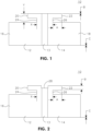
- FIGS 1-3 show exemplary resistor geometries through various stages of adjustment of the Temperature Coefficient of Resistance (TCR). It is understood that the techniques disclosed herein could also apply to other resistor types including film resistors, metal foil resistors and other types of resistor technologies.
- TCR Temperature Coefficient of Resistance
- Figure 1 shows a resistor 10 generally formed of a resistive strip 13 disposed between two conductive strips 12, 14.
- the resistor 10 has main terminals 16, 18 and voltage sense terminals 20, 22. In operation, the main terminals 16, 18 carry the majority of the current passing through the resistor.
- a pair of first and second slots 24, 26 are located between the main terminals and the voltage sense terminals.
- First and second slots 24, 26 each have an associated depth that extends towards the resistive strip 13. This is shown generally as depth A. It is understood that each first and second slots 24, 26 can use the same depth A, or in the alternative, first and second slots 24 and 26 can have different depths.
- Figures 2 and 3 show the formation of a third slot having a depth B and a fourth slot having a depth C. The relationship between these slots will be discussed below.
- the conductive strips are generally formed of copper sheet material and have a thickness typically in the range of about 0.008 - 0.120 inches ( ⁇ 0.2 - 3 mm).
- the thickness of the copper is generally selected based on the desired power dissipation of the device and the desired mechanical strength (e.g., so that the resistor has sufficient strength during manufacture, installation and use).
- the pair of first and second slots 24, 26 partition off a portion of the conductive strips 12, 14 and create a four terminal device.
- the size and location of the pair of first and second slots 24, 26 generally define the dimensions of the main terminals 16, 18 and the voltage sense terminals 20, 22.
- the pair of first and second slots 24, 26 are generally located towards one edge of the resistor.
- the pair of first and second slots 24, 26 are located a distance Y measured from the upper edge of the device.
- the Y distance is generally selected to yield appropriately sized voltage sense terminals.
- the Y distance can be selected to provide voltage sense terminals of sufficient width to withstand punching or machining operations during manufacture and to have sufficient strength during installation and use.
- first and second slots 24, 26 each have a depth generally shown as distance A in Figure 1 . In most applications first and second slots 24, 26 will have the same depth A. It is understood that first and second slots 24 and 26 could each be associated with a different depth. It is also understood that the depth associated with first and second slots 24, 26 could be referenced from a variety of points on the device. Generally, the pair of first and second slots 24, 26 define a reduced thickness or neck between the main terminals 16, 18 and the voltage sense terminals 20, 22. This is shown generally as the distance X in Figure 1 . A description of how the first and second slot depth A is determined is set out below.
- conductive strips 12, 14 are formed of copper.
- copper has a TCR of 3900 ppm/°C.
- the resistive strip 13 may have a TCR of less than 100 ppm/°C.
- the resistor 10 would typically have a very high, positive TCR due to the large amount of copper disposed in the current path. It is generally desirable to minimize the TCR (i.e., a TCR having an absolute value approaching zero).
- a typical range for a given current sense resistor may be ⁇ 25 ppm/°C.
- a given device has a target resistance value of 200 ⁇ (i.e., 0.0002 ⁇ ).
- the initial design without the pair of first and second slots 24, 26 yields a device with a TCR of approximately 800 ppm/°C.
- the thickness of the copper conductive strips 12, 14 is selected as discussed above.
- the dimensions of the resistive strip 13 are selected to yield a resistance that is close to but below the target resistance value. This is done because the final resistance value will be set by a subsequent trimming operation (which will increase the resistance value of the resistor).
- the pair of first and second slots 24, 26 cause the TCR at the voltage sense terminals 20, 22 to become more negative.
- the pair of first and second slots 24, 26 do not significantly alter the TCR of the resistor itself, rather the pair of first and second slots 24, 26 alter the TCR observed at the voltage sense terminals 20, 22.
- first and second slot depth A, and the TCR observed at the voltage sense terminals 20, 22 is determined via a prototyping process. For example, a prototype device is manufactured and then tested using conventional methods (i.e., the voltage, current and temperature is measured through a range of conditions). The depth of the first and second slots 24, 26 is successively increased until a negative starting TCR value is observed at the voltage sense terminals 20, 22, for example approximately -200 ppm/°C. Thus, first and second slots 24, 26 can be thought of as rough TCR calibration slots.
- a negative starting TCR value is desirable at this stage because a third slot will be used to fine tune the TCR value as discussed in more detail below.
- this depth is not altered for a particular style of product (i.e., resistors having the same physical and electrical characteristics). This is advantageous since the pair of first and second slots 24, 26 can be inserted early in the manufacturing process using conventional punching, end milling or other machining techniques. Subsequent slotting operations can be then carried out later in the manufacturing process and can even be accomplished via laser trimming.
- a third slot 28 functioning as a fine TCR calibration slot and having a depth B is shown located between the voltage sense terminals 20, 22.
- the third slot 28 is formed in the resistive strip 13 between the voltage sense terminals 20, 22. It is understood that the second slot can also result in the removal of a portion of the voltage sense terminals 20, 22, as shown in Figure 2 .
- the net effect of the third slot 28 is to drive the TCR observed at the voltage sense terminals 20, 22 positive.
- the third slot 28 will also cause a small increase in resistance value. This is shown graphically in Figure 4 .
- the TCR of the resistor without a third slot 28 is -198 ppm/°C.
- the initial resistance of the device (without third slot 28) is approximately 110 ⁇ (i.e., 0.00011Q).
- the third slot depth set to 0.040" ( ⁇ 1 mm) the TCR improves to -100 ppm/°C.
- the resistance increases to approximately 125 ⁇ (i.e., 0.000125 ⁇ ).
- the third slot 28 functions as a fine TCR calibration slot.
- a typical target range for TCR range for a given device can be approximately ⁇ 25 ppm/°C.
- the third slot 28 can be formed using laser trimming techniques, conventional punching, end milling or any other machining technique that will permit removal of material to a desired depth and width.
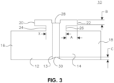
- Figure 3 also shows a fourth slot 30 (resistance calibration slot) formed between main terminals 16, 18.
- the fourth slot 30 has a depth that is selected to fine tune the resistor value. In this case the depth C is selected to yield a target resistance value within specified tolerance (e.g., 200 ⁇ ⁇ 1%).
- the fourth slot 30 can be formed using laser trimming techniques, conventional punching, end milling or any other machining technique techniques that will permit removal of material to a desired depth and width.
- first and second slots 24, 26 and the third slot 28 can be formed at the same time or at separate times. It is also understood that the third slot 28 can be changed "on the fly" (e.g., if TCR is measured on a resistor by resistor basis). Thus the TCR of each resistor could be customized to a specified value. As an added advantage, the third slot 28 can be formed using laser trimming techniques which can greatly simplify the TCR adjustment process.
- First and second slots 24, 26 and third slot 28 shown in Figures 1 and 2 have a generally rectangular profile.
- Fourth slot 30 shown in Figure 3 has a generally triangular profile. It should be understood that other simple or complex geometric slot profiles could be used without departing from the scope of this disclosure.
- Figure 5 shows another slot configuration for TCR compensation.
- Figure 5 shows a resistor 100 generally formed of a resistive strip 113 disposed between two conductive strips 112, 114.
- the conductive strips are generally formed of copper sheet material and have a thickness typically in the range of about 0.008 - 0.120 inches ( ⁇ 0.2 - 3 mm).
- the thickness of the copper is generally selected based on the desired power dissipation of the device and the desired mechanical strength (e.g., so that the resistor has sufficient strength during manufacture, installation and use).
- the resistor 100 has main terminals 116, 118 and voltage sense terminals 120, 122.
- the main terminals 116, 118 carry the majority of the current passing through the resistor.
- the main terminals are formed with a defined internal area (e.g., spaced away from the edges of the conductive strips 112, 114).
- a pair of first and second slots 124, 126 are located between the main terminals and the voltage sense terminals. In this embodiment the voltage sense terminals are formed within the defined internal area of the main terminals. This configuration is desirable for applications requiring more compact and centrally located voltage sense terminals.
- First and second slots 124, 126 are formed with two legs.
- First leg 123 has a length that extends generally orthogonal to the main current path as shown by "A".
- Second leg 125 has a length extends generally parallel to the main current path as shown by "B". It is understood that first and second slots 124 and 126 can use the same leg lengths A and B. In the alternative, first and second slots 124 and 126 can have different leg lengths.
- the resistor 100 also has a third slot 128 having a depth C. The relationship between these slots will be discussed below.
- the pair of first and second slots 124, 126 partition off an internal portion of the conductive strips 112, 114 and create a four terminal device.
- the size and location of the pair of first and second slots 124, 126 generally define the dimensions of the voltage sense terminals 120, 122.
- the sense terminals are located generally in the junction between the first and second legs 123, 125.
- FIG. 6 is a graph showing the TCR compensation associated with the formation of the first and second slots 124, 126.
- Sample 1 is a baseline resistor configured without first and second slots 124, 126. In this configuration, the TCR is +60 ppm/°C.
- Samples 2 and 3 show TCR compensation as the first legs 123 are added (Sample 2) and increased in length (Sample 3). As shown on the graph, the TCR becomes more negative ending at +20 ppm/°C.
- Samples 4 and 5 show TCR compensation as the second legs 125 are added (Sample 4) and increased in length (Sample 5). First legs 123 remain constant in samples 4 and 5. As shown on the graph, the TCR becomes more negative ending at approximately -35 ppm/°C.
- first leg 123 can be inserted first until a rough level of TCR compensation is achieved.
- First legs can be formed by a variety of methods including punching or machining.
- the second leg 125 can be then inserted to fine tune the TCR compensation to the desired level.
- Second legs can be formed by a variety of methods including laser trimming.
- first and second slots 124, 126 will have the same dimensions. It is understood that first and second slots 124 and 126 could each be associated with other leg configurations.
- third slot 128 can be formed to fine tune the resistance value.
- First and second slots 124, 126 and first and second legs 123, 125 as shown in Figure 5 have a generally rectangular profile.
- Third slot 128 shown in Figure 5 has a generally rounded profile. It should be understood that other simple or complex geometric slot or leg profiles could be used without departing from the scope of this disclosure.
Description
- This application claims the benefit of
U.S. Provisional Application No. 61/239,962, filed September 4, 2009 U.S. Provisional Application No. 61/359,000, filed June 28, 2010 - The present invention relates to a four terminal current sense resistor of very low ohmic value and high stability.
- Surface mounted current sense resistors have been available for the electronic market for many years. Their construction typically includes a flat strip of a resistive material that is coupled between high conductivity metal terminals forming the main terminals of the device. A pair of voltage sense terminals can be formed in the main terminals thereby creating a four terminal device. The main terminals carry the majority of the current through the device. The voltage sense terminals produce a voltage that is proportional to the current passing through the device. Such devices provide a mechanism to monitor the current passing through a given circuit using conventional voltage sensing techniques. The actual current passing through the device can be determined based on the sensed voltage and the resistance value of the device as dictated by ohms law. An ideal device would have a Temperature Coefficient of Resistance (TCR) that is close to zero. However, most devices have a non-zero TCR that can lead to inaccurate voltage readings at the voltage sense terminals particularly when the temperature of the device varies.
- In low ohmic current sense resistors and high current shunts, the resistive element length is short while the length of the resistor is a standard length, or in the case of high current shunts long because of the application. The long resistor length and short resistive element length causes a significant amount of copper termination metal to be in the current path. Copper has a TCR of 3900 ppm/°C while the resistive material is typically less than 100 ppm/°C. The added copper in the current path drives the overall TCR of the resistor to values that can be in the 800 ppm/°C range or greater, versus a desired TCR of less than 100 ppm/°C.
- As noted above, typical current sense resistors have four terminals, two main terminals and two voltage sense terminals, separated by two slots. The length of two slots is manipulated to adjust TCR. See
U.S. 5,999,085 (Szwarc) . This method does not lend itself to conventional resistor calibration equipment such as a laser or other cutting techniques that are typically used to reduce the width of the resistive element to increase the resistor's resistance value. - What is needed is an improved configuration and method of making a current sense resistor with TCR compensation or adjustment. It would also be desirable to provide an improved resistor configuration and method that simplifies TCR adjustment of current sense resistor during the manufacturing process. One or more of these aspects will become apparent from the specification and claims that follow.
- The problem posed is solved by the invention as claimed. A resistor according to the invention is defined in claim 1, a method of manufacturing a corresponding resistor is defined in
claim 5. A resistor according to an alternative way of carrying out the invention is defined in claim 11. -
-
Figure 1 illustrates a four terminal resistor with a pair of first and second slots configured to adjust TCR to a negative starting value; -
Figure 2 illustrates a four terminal resistor with a pair of first and second slots and a third slot configured to collectively adjust TCR to a minimum value; -
Figure 3 illustrates a four terminal resistor with a pair of first and second slots and a third slot configured to collectively adjust TCR to a minimum value and a fourth slot configured for resistance calibration; -
Figure 4 is a graph showing the relationship between the third slot depth and TCR and resistance value; -
Figure 5 illustrates another embodiment of a four terminal resistor with TCR compensation; and -
Figure 6 is a graph showing the TCR compensation associated with the various slot formations. -
Figures 1-3 show exemplary resistor geometries through various stages of adjustment of the Temperature Coefficient of Resistance (TCR). It is understood that the techniques disclosed herein could also apply to other resistor types including film resistors, metal foil resistors and other types of resistor technologies. -
Figure 1 , shows aresistor 10 generally formed of aresistive strip 13 disposed between twoconductive strips resistor 10 hasmain terminals voltage sense terminals main terminals second slots second slots resistive strip 13. This is shown generally as depth A. It is understood that each first andsecond slots second slots Figures 2 and3 show the formation of a third slot having a depth B and a fourth slot having a depth C. The relationship between these slots will be discussed below. - Returning to
Figure 1 , the conductive strips are generally formed of copper sheet material and have a thickness typically in the range of about 0.008 - 0.120 inches (~ 0.2 - 3 mm). The thickness of the copper is generally selected based on the desired power dissipation of the device and the desired mechanical strength (e.g., so that the resistor has sufficient strength during manufacture, installation and use). - The pair of first and
second slots conductive strips second slots main terminals voltage sense terminals second slots second slots - The first and
second slots Figure 1 . In most applications first andsecond slots second slots second slots second slots main terminals voltage sense terminals Figure 1 . A description of how the first and second slot depth A is determined is set out below. - In the following example,
conductive strips resistive strip 13 may have a TCR of less than 100 ppm/°C. In absence of the pair of first andsecond slots resistor 10 would typically have a very high, positive TCR due to the large amount of copper disposed in the current path. It is generally desirable to minimize the TCR (i.e., a TCR having an absolute value approaching zero). A typical range for a given current sense resistor may be ± 25 ppm/°C. Assume for this example that a given device has a target resistance value of 200µΩ (i.e., 0.0002Ω). Also assume that the initial design without the pair of first andsecond slots - The thickness of the copper
conductive strips resistive strip 13 are selected to yield a resistance that is close to but below the target resistance value. This is done because the final resistance value will be set by a subsequent trimming operation (which will increase the resistance value of the resistor). - Aside from defining the dimensions of the voltage sense terminals, the pair of first and
second slots voltage sense terminals second slots voltage sense terminals second slots second slots voltage sense terminals - Typically, the relationship between the first and second slot depth A, and the TCR observed at the
voltage sense terminals second slots voltage sense terminals second slots - A negative starting TCR value is desirable at this stage because a third slot will be used to fine tune the TCR value as discussed in more detail below. Once the proper first and second slot depth is determined, this depth is not altered for a particular style of product (i.e., resistors having the same physical and electrical characteristics). This is advantageous since the pair of first and
second slots - Turning to
Figure 2 , athird slot 28 functioning as a fine TCR calibration slot and having a depth B is shown located between thevoltage sense terminals third slot 28 is formed in theresistive strip 13 between thevoltage sense terminals voltage sense terminals Figure 2 . The net effect of thethird slot 28 is to drive the TCR observed at thevoltage sense terminals third slot 28 will also cause a small increase in resistance value. This is shown graphically inFigure 4 . In this example, the TCR of the resistor without a third slot 28 (e.g., as shown inFigure 1 ) is -198 ppm/°C. The initial resistance of the device (without third slot 28) is approximately 110 µΩ (i.e., 0.00011Q). With the third slot depth set to 0.040" (~1 mm) the TCR improves to -100 ppm/°C. Similarly, the resistance increases to approximately 125 µΩ (i.e., 0.000125Ω). - Turning to
Figure 3 , with thethird slot 28 set to at 0.080" (~2mm) the TCR continues to become more positive and approaches zero. The resistance increases to approximately 140 µΩ (i.e., 0.00014Ω). Thus, thethird slot 28 functions as a fine TCR calibration slot. As noted above a typical target range for TCR range for a given device can be approximately ± 25 ppm/°C. Thethird slot 28 can be formed using laser trimming techniques, conventional punching, end milling or any other machining technique that will permit removal of material to a desired depth and width. -
Figure 3 also shows a fourth slot 30 (resistance calibration slot) formed betweenmain terminals fourth slot 30 has a depth that is selected to fine tune the resistor value. In this case the depth C is selected to yield a target resistance value within specified tolerance (e.g., 200 µΩ ± 1%). Thefourth slot 30 can be formed using laser trimming techniques, conventional punching, end milling or any other machining technique techniques that will permit removal of material to a desired depth and width. - It is understood that the first and
second slots third slot 28 can be formed at the same time or at separate times. It is also understood that thethird slot 28 can be changed "on the fly" (e.g., if TCR is measured on a resistor by resistor basis). Thus the TCR of each resistor could be customized to a specified value. As an added advantage, thethird slot 28 can be formed using laser trimming techniques which can greatly simplify the TCR adjustment process. First andsecond slots third slot 28 shown inFigures 1 and 2 have a generally rectangular profile.Fourth slot 30 shown inFigure 3 has a generally triangular profile. It should be understood that other simple or complex geometric slot profiles could be used without departing from the scope of this disclosure. -
Figure 5 shows another slot configuration for TCR compensation.Figure 5 shows aresistor 100 generally formed of aresistive strip 113 disposed between twoconductive strips - The
resistor 100 hasmain terminals voltage sense terminals main terminals conductive strips 112, 114). A pair of first andsecond slots second slots First leg 123 has a length that extends generally orthogonal to the main current path as shown by "A".Second leg 125 has a length extends generally parallel to the main current path as shown by "B". It is understood that first andsecond slots second slots resistor 100 also has athird slot 128 having a depth C. The relationship between these slots will be discussed below. - The pair of first and
second slots conductive strips second slots voltage sense terminals second legs - As discussed above, the
first leg 123 has a length A and thesecond leg 125 has a length B.Figure 6 is a graph showing the TCR compensation associated with the formation of the first andsecond slots second slots C. Samples first legs 123 are added (Sample 2) and increased in length (Sample 3). As shown on the graph, the TCR becomes more negative ending at +20 ppm/°C. Samples second legs 125 are added (Sample 4) and increased in length (Sample 5).First legs 123 remain constant insamples - During manufacturing, the
first leg 123 can be inserted first until a rough level of TCR compensation is achieved. First legs can be formed by a variety of methods including punching or machining. Thesecond leg 125 can be then inserted to fine tune the TCR compensation to the desired level. Second legs can be formed by a variety of methods including laser trimming. In most applications first andsecond slots second slots second slots third slot 128 can be formed to fine tune the resistance value. First andsecond slots second legs Figure 5 have a generally rectangular profile.Third slot 128 shown inFigure 5 has a generally rounded profile. It should be understood that other simple or complex geometric slot or leg profiles could be used without departing from the scope of this disclosure. - Based on the foregoing it is readily apparent that a variety of modifications are possible without departing from the scope of the invention. For example the first and
second slots
Claims (15)
- A resistor (10) with temperature coefficient of resistance, TCR, compensation, the resistor (10) comprising:a resistive strip (13) disposed between two conductive strips (12, 14);first and second main terminals (16, 18) and first and second voltage sense terminals (20, 22) formed in the conductive strips (12, 14),a first slot (24) located between the first main terminal (16) and the first voltage sense terminal (20) and a second slot (26) located between the second main terminal (18) and the second voltage sense terminal (22), -characterized by the first and second slots (24, 26) each having a depth that extends towards the resistive strip (13), the depth being configured to obtain a negative starting TCR value observed at the voltage sense terminals (20, 22), anda fine TCR calibration slot (28) formed between the first and second voltage sense terminals (20, 22), wherein the fine TCR calibration slot (28) has a depth configured to obtain a TCR value observed at the voltage sense terminals (20, 22) that approaches zero.
- The resistor (10) of claim 1 further comprising a resistance calibration slot (30) formed between the first and second main terminals (16, 18), wherein the resistance calibration slot (30) has a depth selected to calibrate a resistance value of the resistor (10).
- The resistor (10) of claim 1 wherein the fine TCR calibration slot (28) is formed in the resistive strip (13).
- The resistor (10) of claim 1 wherein the fine TCR calibration slot (28) is formed in the resistive strip (13) and at least one of the first or second voltage sense terminals (20, 22).
- A method of manufacturing a resistor (10) with temperature coefficient of resistance, TCR, compensation, the method comprising:disposing a resistive strip (13) between two conductive strips (12, 14);forming first and second main terminals (16, 18) and first and second voltage sense terminals (20, 22) in the conductive strips (12, 14),forming a first slot (24) between the first main terminal (16) and the first voltage sense terminal (20) and a second slot (26) between the second main terminal (18) and the second voltage sense terminal (22), characterized by the first and second slots (24, 26) each having a depth that extends towards the resistive strip (13), the depth being configured to obtain a negative starting TCR value observed at the voltage sense terminals (20, 22), andforming a fine TCR calibration slot (28) between the first and second voltage sense terminals (20, 22), wherein the fine TCR calibration slot (28) has a depth configured to obtain a TCR value observed at the voltage sense terminals (20, 22) that approaches zero.
- The method of claim 5 further comprising forming a resistance calibration slot (30) between the first and second main terminals (16, 18), wherein the resistance calibration slot (30) has a depth selected to calibrate a resistance value of the resistor (10).
- The method of claim 5 further comprising forming the fine TCR calibration slot (28) in the resistive strip (13).
- The method of claim 5 further comprising forming the fine TCR calibration slot (28) in the resistive strip (13) and at least one of the voltage sense terminals (20, 22).
- The method of claim 5 further comprising forming the first and second slots (24, 26) by punching or machining.
- The method of claim 5 further comprising forming the fine TCR calibration slot (28) by laser trimming.
- A resistor (100) with temperature coefficient of resistance (TCR) compensation, the resistor (100) comprising:a resistive strip (113) disposed between two conductive strips (112, 114), each of the conductive strips (112, 114) have a defined internal area spaced away from the-edges of each of the conductive strips;first and second main terminals (116, 118) and first and second voltage sense terminals (120, 122) formed within the defined internal area of the conductive strips (112, 114), -and first and second TCR calibration slots (124, 126) characterized by thefirst and second TCR calibration slots (124, 126) each having a first TCR calibration leg (123) located between the first main terminal (116) and the first voltage sense terminal (120) and between the second main terminal (118) and the second voltage sense terminal (122), the first TCR calibration legs (123) having a length configured to obtain a TCR value observed at the voltage sense terminals (120, 122) that is lower than a TCR value observed without the first calibration legs (123), andthe first and second TCR calibration slots (124, 126) each having second TCR calibration legs (125) formed between the first and second main terminals (116, 118), wherein the second TCR calibration legs (125) have a length configured to obtain a TCR value observed at the voltage sense terminals (120, 122) that approaches zero.
- The resistor (100) of claim 11 wherein the two conductive strips (112, 114) define a main current path and the first TCR calibration legs (123) are disposed generally orthogonal to the main current path.
- The resistor (100) of claim 12 wherein the second TCR calibration legs (125) are disposed generally parallel to the main current path.
- The resistor (100) of claim 11 wherein each of the first and second TCR calibration legs (123, 125) form junctions that define a location of the first and second voltage sense terminals (120, 122).
- The resistor (100) of claim 11 further comprising a resistance calibration slot (128) formed in the resistive strip (113).
Priority Applications (1)
| Application Number | Priority Date | Filing Date | Title |
|---|---|---|---|
| EP23201364.9A EP4280232A2 (en) | 2009-09-04 | 2010-09-02 | Resistor with temperature coefficient of resistance (tcr) compensation |
Applications Claiming Priority (3)
| Application Number | Priority Date | Filing Date | Title |
|---|---|---|---|
| US23996209P | 2009-09-04 | 2009-09-04 | |
| US35900010P | 2010-06-28 | 2010-06-28 | |
| PCT/US2010/047628 WO2011028870A1 (en) | 2009-09-04 | 2010-09-02 | Resistor with temperature coefficient of resistance (tcr) compensation |
Related Child Applications (1)
| Application Number | Title | Priority Date | Filing Date |
|---|---|---|---|
| EP23201364.9A Division EP4280232A2 (en) | 2009-09-04 | 2010-09-02 | Resistor with temperature coefficient of resistance (tcr) compensation |
Publications (3)
| Publication Number | Publication Date |
|---|---|
| EP2474008A1 EP2474008A1 (en) | 2012-07-11 |
| EP2474008A4 EP2474008A4 (en) | 2018-03-28 |
| EP2474008B1 true EP2474008B1 (en) | 2023-10-04 |
Family
ID=43647284
Family Applications (2)
| Application Number | Title | Priority Date | Filing Date |
|---|---|---|---|
| EP10814475.9A Active EP2474008B1 (en) | 2009-09-04 | 2010-09-02 | Resistor with temperature coefficient of resistance (tcr) compensation |
| EP23201364.9A Pending EP4280232A2 (en) | 2009-09-04 | 2010-09-02 | Resistor with temperature coefficient of resistance (tcr) compensation |
Family Applications After (1)
| Application Number | Title | Priority Date | Filing Date |
|---|---|---|---|
| EP23201364.9A Pending EP4280232A2 (en) | 2009-09-04 | 2010-09-02 | Resistor with temperature coefficient of resistance (tcr) compensation |
Country Status (10)
| Country | Link |
|---|---|
| US (9) | US8198977B2 (en) |
| EP (2) | EP2474008B1 (en) |
| JP (5) | JP5545784B2 (en) |
| KR (7) | KR101603005B1 (en) |
| CN (2) | CN105679474B (en) |
| HK (2) | HK1175296A1 (en) |
| IL (2) | IL218453A (en) |
| IN (1) | IN2012DN01923A (en) |
| TW (3) | TWI544502B (en) |
| WO (1) | WO2011028870A1 (en) |
Families Citing this family (25)
| Publication number | Priority date | Publication date | Assignee | Title |
|---|---|---|---|---|
| IN2012DN01923A (en) * | 2009-09-04 | 2015-07-24 | Vishay Dale Electronics Inc | |
| US9305687B2 (en) | 2010-05-13 | 2016-04-05 | Cyntec Co., Ltd. | Current sensing resistor |
| US8779887B2 (en) | 2010-05-13 | 2014-07-15 | Cyntec Co., Ltd. | Current sensing resistor |
| DE102010035485A1 (en) | 2010-08-26 | 2012-03-01 | Isabellenhütte Heusler Gmbh & Co. Kg | Current sense resistor |
| CN104376938B (en) * | 2013-08-13 | 2018-03-13 | 乾坤科技股份有限公司 | Resistance device |
| US20150276881A1 (en) * | 2014-03-25 | 2015-10-01 | The Boeing Company | Model-independent battery life and performance forecaster |
| JP6509022B2 (en) * | 2015-04-28 | 2019-05-08 | サンコール株式会社 | Method of manufacturing shunt resistor |
| JP6795879B2 (en) * | 2015-06-15 | 2020-12-02 | Koa株式会社 | Resistor and its manufacturing method |
| JP6842823B2 (en) * | 2015-06-22 | 2021-03-17 | Koa株式会社 | Current detection resistor |
| US9595518B1 (en) | 2015-12-15 | 2017-03-14 | Globalfoundries Inc. | Fin-type metal-semiconductor resistors and fabrication methods thereof |
| DE102016014130B3 (en) * | 2016-11-25 | 2017-11-23 | Isabellenhütte Heusler Gmbh & Co. Kg | Current measuring device |
| JP2018132386A (en) * | 2017-02-14 | 2018-08-23 | Koa株式会社 | Current measurement device and resistor for detecting current |
| WO2018229817A1 (en) * | 2017-06-12 | 2018-12-20 | 新電元工業株式会社 | Power module |
| EP3853620B1 (en) * | 2018-09-21 | 2023-11-08 | Continental Automotive Technologies GmbH | Battery sensor for temperature-independent current measurement using a shunt |
| US11415601B2 (en) * | 2018-12-21 | 2022-08-16 | Cyntec Co., Ltd. | Resistor having low temperature coefficient of resistance |
| JP7210335B2 (en) * | 2019-03-08 | 2023-01-23 | サンコール株式会社 | Shunt resistor and its manufacturing method |
| TWM581283U (en) * | 2019-04-02 | 2019-07-21 | 光頡科技股份有限公司 | Four-terminal resistor |
| US11361635B2 (en) | 2019-05-07 | 2022-06-14 | Invue Security Products Inc. | Merchandise display security systems and methods |
| WO2021161237A1 (en) * | 2020-02-12 | 2021-08-19 | Sendyne Corporation | Method of predicting thermal resistive behavior of shunts |
| WO2021220526A1 (en) * | 2020-04-27 | 2021-11-04 | Koa株式会社 | Shunt resistor, shunt resistor manufacturing method, and current detecting device |
| IL300693B2 (en) * | 2020-08-20 | 2024-02-01 | Vishay Dale Electronics Llc | Resistors, current sense resistors, battery shunts, shunt resistors, and methods of making |
| DE102020007556A1 (en) * | 2020-12-10 | 2022-06-15 | Wieland-Werke Aktiengesellschaft | Resistor arrangement and method for its manufacture |
| DE102021103241A1 (en) | 2021-02-11 | 2022-08-11 | Isabellenhütte Heusler Gmbh & Co. Kg | current sensing resistor |
| JP7435505B2 (en) * | 2021-03-04 | 2024-02-21 | トヨタ自動車株式会社 | Resistance spot welding method and resistance spot welding device |
| JP2023087730A (en) | 2021-12-14 | 2023-06-26 | Koa株式会社 | Shunt resistor and current detection device |
Family Cites Families (68)
| Publication number | Priority date | Publication date | Assignee | Title |
|---|---|---|---|---|
| US4079349A (en) * | 1976-09-29 | 1978-03-14 | Corning Glass Works | Low TCR resistor |
| US4200970A (en) * | 1977-04-14 | 1980-05-06 | Milton Schonberger | Method of adjusting resistance of a thermistor |
| JPS57117204A (en) * | 1981-01-14 | 1982-07-21 | Hitachi Ltd | Method of forming thick film resistor |
| DE3113745A1 (en) * | 1981-04-04 | 1982-10-21 | Robert Bosch Gmbh, 7000 Stuttgart | THIN LAYER STRETCH MEASUREMENT STRIP AND METHOD FOR THE PRODUCTION THEREOF |
| FR2529374B1 (en) * | 1982-06-25 | 1985-06-21 | Renix Electronique Sa | RESISTIVE CIRCUIT ELEMENT AND MANUFACTURING METHOD THEREOF |
| US4529958A (en) * | 1983-05-02 | 1985-07-16 | Dale Electronics, Inc. | Electrical resistor |
| US4907341A (en) * | 1987-02-27 | 1990-03-13 | John Fluke Mfg. Co., Inc. | Compound resistor manufacturing method |
| JPH0325994A (en) * | 1989-06-23 | 1991-02-04 | Nec Corp | Hybrid integrated circuit |
| US5015989A (en) * | 1989-07-28 | 1991-05-14 | Pacific Hybrid Microelectronics, Inc. | Film resistor with enhanced trimming characteristics |
| JPH02110903A (en) | 1989-08-31 | 1990-04-24 | Murata Mfg Co Ltd | Manufacture of resistor |
| JP3049843B2 (en) * | 1991-04-26 | 2000-06-05 | 株式会社デンソー | Method of forming resistor electrode structure |
| US5214407A (en) | 1991-11-06 | 1993-05-25 | Hewlett-Packard Company | High performance current shunt |
| US5287083A (en) * | 1992-03-30 | 1994-02-15 | Dale Electronics, Inc. | Bulk metal chip resistor |
| DE4243349A1 (en) | 1992-12-21 | 1994-06-30 | Heusler Isabellenhuette | Manufacture of resistors from composite material |
| JP3284375B2 (en) * | 1993-03-10 | 2002-05-20 | コーア株式会社 | Current detecting resistor and method of manufacturing the same |
| BE1007868A3 (en) * | 1993-12-10 | 1995-11-07 | Koninkl Philips Electronics Nv | Electrical resistance. |
| US5604477A (en) * | 1994-12-07 | 1997-02-18 | Dale Electronics, Inc. | Surface mount resistor and method for making same |
| US5621240A (en) * | 1995-09-05 | 1997-04-15 | Delco Electronics Corp. | Segmented thick film resistors |
| JP3637124B2 (en) | 1996-01-10 | 2005-04-13 | ローム株式会社 | Structure of chip resistor and manufacturing method thereof |
| DE69715091T2 (en) | 1996-05-29 | 2003-01-02 | Matsushita Electric Ind Co Ltd | Surface mount resistor |
| EP0870306B1 (en) | 1996-10-30 | 2005-07-27 | Koninklijke Philips Electronics N.V. | Method of securing an electric contact to a ceramic layer as well as a resistance element thus manufactured |
| JPH10289803A (en) * | 1997-04-16 | 1998-10-27 | Matsushita Electric Ind Co Ltd | Resistor and manufacture thereof |
| US5953811A (en) * | 1998-01-20 | 1999-09-21 | Emc Technology Llc | Trimming temperature variable resistor |
| US5999085A (en) | 1998-02-13 | 1999-12-07 | Vishay Dale Electronics, Inc. | Surface mounted four terminal resistor |
| JPH11283802A (en) * | 1998-03-30 | 1999-10-15 | Kyocera Corp | Chip resistor |
| GB9813982D0 (en) * | 1998-06-30 | 1998-08-26 | Mem Limited | Residual current detection device |
| DE19906276A1 (en) | 1999-02-15 | 2000-09-21 | Heusler Isabellenhuette | Method and current measuring module for current monitoring in a power supply system |
| JP2000269012A (en) | 1999-03-17 | 2000-09-29 | Kooa T & T Kk | Chip-type electronic components with resistance element and its manufacture |
| JP3366916B2 (en) | 1999-06-03 | 2003-01-14 | スミダコーポレーション株式会社 | Inductance element |
| JP2001155902A (en) * | 1999-11-30 | 2001-06-08 | Taiyosha Denki Kk | Chip resistor and its manufacturing method |
| US6401329B1 (en) * | 1999-12-21 | 2002-06-11 | Vishay Dale Electronics, Inc. | Method for making overlay surface mount resistor |
| US6181234B1 (en) | 1999-12-29 | 2001-01-30 | Vishay Dale Electronics, Inc. | Monolithic heat sinking resistor |
| JP4722318B2 (en) | 2000-06-05 | 2011-07-13 | ローム株式会社 | Chip resistor |
| JP2002025802A (en) | 2000-07-10 | 2002-01-25 | Rohm Co Ltd | Chip resistor |
| JP2002050501A (en) * | 2000-08-01 | 2002-02-15 | K-Tech Devices Corp | Mounting body and using method thereof |
| JP3967553B2 (en) | 2001-03-09 | 2007-08-29 | ローム株式会社 | Chip resistor manufacturing method and chip resistor |
| JP3958532B2 (en) | 2001-04-16 | 2007-08-15 | ローム株式会社 | Manufacturing method of chip resistor |
| CN2490589Y (en) * | 2001-07-20 | 2002-05-08 | 成都希望电子研究所 | Current sampling resistance |
| DE20117650U1 (en) * | 2001-10-29 | 2003-03-13 | Heusler Isabellenhuette | Surface mount electrical resistance |
| JP2003197403A (en) * | 2001-12-26 | 2003-07-11 | Koa Corp | Low-resistance resistor |
| US7342480B2 (en) | 2002-06-13 | 2008-03-11 | Rohm Co., Ltd. | Chip resistor and method of making same |
| JP2004047603A (en) * | 2002-07-10 | 2004-02-12 | Matsushita Electric Ind Co Ltd | Resistor for current detection and its manufacture |
| US20040216303A1 (en) * | 2003-05-01 | 2004-11-04 | Berlin Carl W. | Thick film current sensing resistor and method |
| DE10328870A1 (en) | 2003-06-26 | 2005-01-20 | Isabellenhütte Heusler GmbH KG | Resistance arrangement, manufacturing method and measuring circuit |
| JP2005181056A (en) * | 2003-12-18 | 2005-07-07 | Microjenics Inc | Resistor for current detection |
| JP4391918B2 (en) * | 2004-10-13 | 2009-12-24 | コーア株式会社 | Current detection resistor |
| JP2007221006A (en) * | 2006-02-17 | 2007-08-30 | Sanken Electric Co Ltd | Resistor including resistance element and method of resistance value inspection performed by resistor |
| US20090205196A1 (en) * | 2006-03-23 | 2009-08-20 | Oleg Grudin | Self-heating effects during operation of thermally-trimmable resistors |
| JP4971693B2 (en) * | 2006-06-09 | 2012-07-11 | コーア株式会社 | Metal plate resistor |
| US8018310B2 (en) | 2006-09-27 | 2011-09-13 | Vishay Dale Electronics, Inc. | Inductor with thermally stable resistance |
| US7843309B2 (en) | 2007-09-27 | 2010-11-30 | Vishay Dale Electronics, Inc. | Power resistor |
| JP5179155B2 (en) | 2007-12-07 | 2013-04-10 | 太陽社電気株式会社 | Chip resistor |
| US8031043B2 (en) | 2008-01-08 | 2011-10-04 | Infineon Technologies Ag | Arrangement comprising a shunt resistor and method for producing an arrangement comprising a shunt resistor |
| US7911319B2 (en) * | 2008-02-06 | 2011-03-22 | Vishay Dale Electronics, Inc. | Resistor, and method for making same |
| US8242878B2 (en) | 2008-09-05 | 2012-08-14 | Vishay Dale Electronics, Inc. | Resistor and method for making same |
| WO2010052697A1 (en) | 2008-11-06 | 2010-05-14 | Vishay Intertechnology, Inc. | Four-terminal resistor with four resistors and adjustable temperature coefficient of resistance |
| US8248202B2 (en) | 2009-03-19 | 2012-08-21 | Vishay Dale Electronics, Inc. | Metal strip resistor for mitigating effects of thermal EMF |
| DE202009010319U1 (en) * | 2009-07-01 | 2009-11-19 | Isabellenhütte Heusler Gmbh & Co. Kg | Electronic component |
| IN2012DN01923A (en) * | 2009-09-04 | 2015-07-24 | Vishay Dale Electronics Inc | |
| TWI381170B (en) | 2009-09-17 | 2013-01-01 | Cyntec Co Ltd | Current sensing resistor device and process |
| DE102010035485A1 (en) * | 2010-08-26 | 2012-03-01 | Isabellenhütte Heusler Gmbh & Co. Kg | Current sense resistor |
| ITTO20120293A1 (en) * | 2012-04-03 | 2013-10-04 | Metallux Sa | PROCEDURE FOR CALIBRATING A CALIBRATION ELEMENT AND ITS DEVICE |
| US9396849B1 (en) | 2014-03-10 | 2016-07-19 | Vishay Dale Electronics Llc | Resistor and method of manufacture |
| JP6795879B2 (en) * | 2015-06-15 | 2020-12-02 | Koa株式会社 | Resistor and its manufacturing method |
| US10438730B2 (en) | 2017-10-31 | 2019-10-08 | Cyntec Co., Ltd. | Current sensing resistor and fabrication method thereof |
| US11415601B2 (en) | 2018-12-21 | 2022-08-16 | Cyntec Co., Ltd. | Resistor having low temperature coefficient of resistance |
| IL300693B2 (en) | 2020-08-20 | 2024-02-01 | Vishay Dale Electronics Llc | Resistors, current sense resistors, battery shunts, shunt resistors, and methods of making |
| DE202021103627U1 (en) | 2021-07-06 | 2021-07-15 | Vishay Dale Electronics, Llc | Electrical resistance |
-
2010
- 2010-09-02 IN IN1923DEN2012 patent/IN2012DN01923A/en unknown
- 2010-09-02 KR KR1020137028154A patent/KR101603005B1/en active Application Filing
- 2010-09-02 KR KR1020177025439A patent/KR101895742B1/en active IP Right Grant
- 2010-09-02 EP EP10814475.9A patent/EP2474008B1/en active Active
- 2010-09-02 US US12/874,514 patent/US8198977B2/en active Active
- 2010-09-02 KR KR1020167005915A patent/KR20160032255A/en active Application Filing
- 2010-09-02 CN CN201610094458.7A patent/CN105679474B/en active Active
- 2010-09-02 KR KR1020127008673A patent/KR101398145B1/en active IP Right Grant
- 2010-09-02 KR KR1020177013849A patent/KR20170061185A/en not_active Application Discontinuation
- 2010-09-02 CN CN201080039614.0A patent/CN102696079B/en active Active
- 2010-09-02 KR KR1020147016551A patent/KR20140094619A/en not_active Application Discontinuation
- 2010-09-02 JP JP2012528034A patent/JP5545784B2/en active Active
- 2010-09-02 WO PCT/US2010/047628 patent/WO2011028870A1/en active Application Filing
- 2010-09-02 KR KR1020187035465A patent/KR102115114B1/en active IP Right Grant
- 2010-09-02 EP EP23201364.9A patent/EP4280232A2/en active Pending
- 2010-09-03 TW TW099129838A patent/TWI544502B/en active
- 2010-09-03 TW TW105120298A patent/TWI590265B/en active
- 2010-09-03 TW TW103133717A patent/TWI590264B/en active
-
2012
- 2012-03-04 IL IL218453A patent/IL218453A/en active IP Right Grant
- 2012-06-11 US US13/493,402 patent/US8525637B2/en active Active
-
2013
- 2013-02-19 HK HK13102068.8A patent/HK1175296A1/en unknown
- 2013-08-30 US US14/015,488 patent/US8878643B2/en active Active
-
2014
- 2014-01-08 JP JP2014001810A patent/JP5778794B2/en active Active
- 2014-03-27 IL IL231753A patent/IL231753B/en active IP Right Grant
- 2014-05-07 JP JP2014096081A patent/JP6044964B2/en active Active
- 2014-11-03 US US14/531,505 patent/US9400294B2/en active Active
-
2015
- 2015-08-14 JP JP2015160132A patent/JP6586315B2/en active Active
-
2016
- 2016-07-25 US US15/218,219 patent/US9779860B2/en active Active
- 2016-12-06 HK HK16113908A patent/HK1225852A1/en unknown
-
2017
- 2017-10-02 US US15/722,536 patent/US10217550B2/en active Active
-
2018
- 2018-05-17 JP JP2018095582A patent/JP2018160675A/en active Pending
-
2019
- 2019-02-25 US US16/284,592 patent/US10796826B2/en active Active
-
2020
- 2020-10-05 US US17/063,235 patent/US11562838B2/en active Active
-
2023
- 2023-01-23 US US18/158,289 patent/US20230343495A1/en active Pending
Also Published As
Similar Documents
| Publication | Publication Date | Title |
|---|---|---|
| EP2474008B1 (en) | Resistor with temperature coefficient of resistance (tcr) compensation |
Legal Events
| Date | Code | Title | Description |
|---|---|---|---|
| PUAI | Public reference made under article 153(3) epc to a published international application that has entered the european phase |
Free format text: ORIGINAL CODE: 0009012 |
|
| STAA | Information on the status of an ep patent application or granted ep patent |
Free format text: STATUS: REQUEST FOR EXAMINATION WAS MADE |
|
| 17P | Request for examination filed |
Effective date: 20120328 |
|
| AK | Designated contracting states |
Kind code of ref document: A1 Designated state(s): AL AT BE BG CH CY CZ DE DK EE ES FI FR GB GR HR HU IE IS IT LI LT LU LV MC MK MT NL NO PL PT RO SE SI SK SM TR |
|
| DAX | Request for extension of the european patent (deleted) | ||
| RA4 | Supplementary search report drawn up and despatched (corrected) |
Effective date: 20180227 |
|
| RIC1 | Information provided on ipc code assigned before grant |
Ipc: G01R 19/00 20060101ALI20180221BHEP Ipc: H01C 17/232 20060101ALI20180221BHEP Ipc: G01R 1/20 20060101ALI20180221BHEP Ipc: H01C 1/148 20060101ALI20180221BHEP Ipc: H01C 17/28 20060101ALI20180221BHEP Ipc: H01C 1/00 20060101ALI20180221BHEP Ipc: G01R 19/32 20060101ALI20180221BHEP Ipc: H01C 7/06 20060101AFI20180221BHEP |
|
| GRAJ | Information related to disapproval of communication of intention to grant by the applicant or resumption of examination proceedings by the epo deleted |
Free format text: ORIGINAL CODE: EPIDOSDIGR1 |
|
| GRAP | Despatch of communication of intention to grant a patent |
Free format text: ORIGINAL CODE: EPIDOSNIGR1 |
|
| STAA | Information on the status of an ep patent application or granted ep patent |
Free format text: STATUS: REQUEST FOR EXAMINATION WAS MADE |
|
| GRAP | Despatch of communication of intention to grant a patent |
Free format text: ORIGINAL CODE: EPIDOSNIGR1 |
|
| STAA | Information on the status of an ep patent application or granted ep patent |
Free format text: STATUS: GRANT OF PATENT IS INTENDED |
|
| INTG | Intention to grant announced |
Effective date: 20210604 |
|
| GRAJ | Information related to disapproval of communication of intention to grant by the applicant or resumption of examination proceedings by the epo deleted |
Free format text: ORIGINAL CODE: EPIDOSDIGR1 |
|
| STAA | Information on the status of an ep patent application or granted ep patent |
Free format text: STATUS: REQUEST FOR EXAMINATION WAS MADE |
|
| INTC | Intention to grant announced (deleted) | ||
| GRAP | Despatch of communication of intention to grant a patent |
Free format text: ORIGINAL CODE: EPIDOSNIGR1 |
|
| STAA | Information on the status of an ep patent application or granted ep patent |
Free format text: STATUS: GRANT OF PATENT IS INTENDED |
|
| INTG | Intention to grant announced |
Effective date: 20211202 |
|
| GRAJ | Information related to disapproval of communication of intention to grant by the applicant or resumption of examination proceedings by the epo deleted |
Free format text: ORIGINAL CODE: EPIDOSDIGR1 |
|
| STAA | Information on the status of an ep patent application or granted ep patent |
Free format text: STATUS: REQUEST FOR EXAMINATION WAS MADE |
|
| INTC | Intention to grant announced (deleted) | ||
| GRAP | Despatch of communication of intention to grant a patent |
Free format text: ORIGINAL CODE: EPIDOSNIGR1 |
|
| STAA | Information on the status of an ep patent application or granted ep patent |
Free format text: STATUS: GRANT OF PATENT IS INTENDED |
|
| INTG | Intention to grant announced |
Effective date: 20220704 |
|
| GRAJ | Information related to disapproval of communication of intention to grant by the applicant or resumption of examination proceedings by the epo deleted |
Free format text: ORIGINAL CODE: EPIDOSDIGR1 |
|
| STAA | Information on the status of an ep patent application or granted ep patent |
Free format text: STATUS: REQUEST FOR EXAMINATION WAS MADE |
|
| INTC | Intention to grant announced (deleted) | ||
| GRAP | Despatch of communication of intention to grant a patent |
Free format text: ORIGINAL CODE: EPIDOSNIGR1 |
|
| STAA | Information on the status of an ep patent application or granted ep patent |
Free format text: STATUS: GRANT OF PATENT IS INTENDED |
|
| INTG | Intention to grant announced |
Effective date: 20230404 |
|
| GRAS | Grant fee paid |
Free format text: ORIGINAL CODE: EPIDOSNIGR3 |
|
| GRAA | (expected) grant |
Free format text: ORIGINAL CODE: 0009210 |
|
| STAA | Information on the status of an ep patent application or granted ep patent |
Free format text: STATUS: THE PATENT HAS BEEN GRANTED |
|
| AK | Designated contracting states |
Kind code of ref document: B1 Designated state(s): AL AT BE BG CH CY CZ DE DK EE ES FI FR GB GR HR HU IE IS IT LI LT LU LV MC MK MT NL NO PL PT RO SE SI SK SM TR |
|
| REG | Reference to a national code |
Ref country code: GB Ref legal event code: FG4D |
|
| REG | Reference to a national code |
Ref country code: CH Ref legal event code: EP |
|
| REG | Reference to a national code |
Ref country code: DE Ref legal event code: R096 Ref document number: 602010069070 Country of ref document: DE |
|
| REG | Reference to a national code |
Ref country code: IE Ref legal event code: FG4D |
|
| REG | Reference to a national code |
Ref country code: LT Ref legal event code: MG9D |
|
| REG | Reference to a national code |
Ref country code: NL Ref legal event code: MP Effective date: 20231004 |
|
| REG | Reference to a national code |
Ref country code: DE Ref legal event code: R081 Ref document number: 602010069070 Country of ref document: DE Owner name: VISHAY DALE ELECTRONICS, LLC, COLUMBUS, US Free format text: FORMER OWNER: VISHAY DALE ELECTRONICS, INC., COLUMBUS, NE, US |
|
| RAP4 | Party data changed (patent owner data changed or rights of a patent transferred) |
Owner name: VISHAY DALE ELECTRONICS, LLC |
|
| REG | Reference to a national code |
Ref country code: AT Ref legal event code: MK05 Ref document number: 1618633 Country of ref document: AT Kind code of ref document: T Effective date: 20231004 |
|
| PG25 | Lapsed in a contracting state [announced via postgrant information from national office to epo] |
Ref country code: NL Free format text: LAPSE BECAUSE OF FAILURE TO SUBMIT A TRANSLATION OF THE DESCRIPTION OR TO PAY THE FEE WITHIN THE PRESCRIBED TIME-LIMIT Effective date: 20231004 |
|
| PG25 | Lapsed in a contracting state [announced via postgrant information from national office to epo] |
Ref country code: GR Free format text: LAPSE BECAUSE OF FAILURE TO SUBMIT A TRANSLATION OF THE DESCRIPTION OR TO PAY THE FEE WITHIN THE PRESCRIBED TIME-LIMIT Effective date: 20240105 |
|
| PG25 | Lapsed in a contracting state [announced via postgrant information from national office to epo] |
Ref country code: IS Free format text: LAPSE BECAUSE OF FAILURE TO SUBMIT A TRANSLATION OF THE DESCRIPTION OR TO PAY THE FEE WITHIN THE PRESCRIBED TIME-LIMIT Effective date: 20240204 |
|
| PG25 | Lapsed in a contracting state [announced via postgrant information from national office to epo] |
Ref country code: LT Free format text: LAPSE BECAUSE OF FAILURE TO SUBMIT A TRANSLATION OF THE DESCRIPTION OR TO PAY THE FEE WITHIN THE PRESCRIBED TIME-LIMIT Effective date: 20231004 |