EP2472615A2 - Sealing member, sealing method, and method for producing optical semiconductor device - Google Patents
Sealing member, sealing method, and method for producing optical semiconductor device Download PDFInfo
- Publication number
- EP2472615A2 EP2472615A2 EP11192972A EP11192972A EP2472615A2 EP 2472615 A2 EP2472615 A2 EP 2472615A2 EP 11192972 A EP11192972 A EP 11192972A EP 11192972 A EP11192972 A EP 11192972A EP 2472615 A2 EP2472615 A2 EP 2472615A2
- Authority
- EP
- European Patent Office
- Prior art keywords
- sealing
- resin layer
- sealing resin
- releasing film
- sealing member
- Prior art date
- Legal status (The legal status is an assumption and is not a legal conclusion. Google has not performed a legal analysis and makes no representation as to the accuracy of the status listed.)
- Granted
Links
Images



Classifications
-
- H—ELECTRICITY
- H10—SEMICONDUCTOR DEVICES; ELECTRIC SOLID-STATE DEVICES NOT OTHERWISE PROVIDED FOR
- H10H—INORGANIC LIGHT-EMITTING SEMICONDUCTOR DEVICES HAVING POTENTIAL BARRIERS
- H10H20/00—Individual inorganic light-emitting semiconductor devices having potential barriers, e.g. light-emitting diodes [LED]
- H10H20/80—Constructional details
- H10H20/85—Packages
- H10H20/852—Encapsulations
-
- B—PERFORMING OPERATIONS; TRANSPORTING
- B29—WORKING OF PLASTICS; WORKING OF SUBSTANCES IN A PLASTIC STATE IN GENERAL
- B29C—SHAPING OR JOINING OF PLASTICS; SHAPING OF MATERIAL IN A PLASTIC STATE, NOT OTHERWISE PROVIDED FOR; AFTER-TREATMENT OF THE SHAPED PRODUCTS, e.g. REPAIRING
- B29C43/00—Compression moulding, i.e. applying external pressure to flow the moulding material; Apparatus therefor
- B29C43/02—Compression moulding, i.e. applying external pressure to flow the moulding material; Apparatus therefor of articles of definite length, i.e. discrete articles
- B29C43/18—Compression moulding, i.e. applying external pressure to flow the moulding material; Apparatus therefor of articles of definite length, i.e. discrete articles incorporating preformed parts or layers, e.g. compression moulding around inserts or for coating articles
-
- B—PERFORMING OPERATIONS; TRANSPORTING
- B29—WORKING OF PLASTICS; WORKING OF SUBSTANCES IN A PLASTIC STATE IN GENERAL
- B29C—SHAPING OR JOINING OF PLASTICS; SHAPING OF MATERIAL IN A PLASTIC STATE, NOT OTHERWISE PROVIDED FOR; AFTER-TREATMENT OF THE SHAPED PRODUCTS, e.g. REPAIRING
- B29C43/00—Compression moulding, i.e. applying external pressure to flow the moulding material; Apparatus therefor
- B29C43/02—Compression moulding, i.e. applying external pressure to flow the moulding material; Apparatus therefor of articles of definite length, i.e. discrete articles
- B29C43/20—Making multilayered or multicoloured articles
- B29C43/203—Making multilayered articles
-
- B—PERFORMING OPERATIONS; TRANSPORTING
- B32—LAYERED PRODUCTS
- B32B—LAYERED PRODUCTS, i.e. PRODUCTS BUILT-UP OF STRATA OF FLAT OR NON-FLAT, e.g. CELLULAR OR HONEYCOMB, FORM
- B32B37/00—Methods or apparatus for laminating, e.g. by curing or by ultrasonic bonding
- B32B37/14—Methods or apparatus for laminating, e.g. by curing or by ultrasonic bonding characterised by the properties of the layers
- B32B37/16—Methods or apparatus for laminating, e.g. by curing or by ultrasonic bonding characterised by the properties of the layers with all layers existing as coherent layers before laminating
-
- B—PERFORMING OPERATIONS; TRANSPORTING
- B29—WORKING OF PLASTICS; WORKING OF SUBSTANCES IN A PLASTIC STATE IN GENERAL
- B29C—SHAPING OR JOINING OF PLASTICS; SHAPING OF MATERIAL IN A PLASTIC STATE, NOT OTHERWISE PROVIDED FOR; AFTER-TREATMENT OF THE SHAPED PRODUCTS, e.g. REPAIRING
- B29C33/00—Moulds or cores; Details thereof or accessories therefor
- B29C33/56—Coatings, e.g. enameled or galvanised; Releasing, lubricating or separating agents
- B29C33/68—Release sheets
-
- H—ELECTRICITY
- H10—SEMICONDUCTOR DEVICES; ELECTRIC SOLID-STATE DEVICES NOT OTHERWISE PROVIDED FOR
- H10H—INORGANIC LIGHT-EMITTING SEMICONDUCTOR DEVICES HAVING POTENTIAL BARRIERS
- H10H20/00—Individual inorganic light-emitting semiconductor devices having potential barriers, e.g. light-emitting diodes [LED]
- H10H20/01—Manufacture or treatment
- H10H20/036—Manufacture or treatment of packages
- H10H20/0361—Manufacture or treatment of packages of wavelength conversion means
-
- H—ELECTRICITY
- H10—SEMICONDUCTOR DEVICES; ELECTRIC SOLID-STATE DEVICES NOT OTHERWISE PROVIDED FOR
- H10H—INORGANIC LIGHT-EMITTING SEMICONDUCTOR DEVICES HAVING POTENTIAL BARRIERS
- H10H20/00—Individual inorganic light-emitting semiconductor devices having potential barriers, e.g. light-emitting diodes [LED]
- H10H20/01—Manufacture or treatment
- H10H20/036—Manufacture or treatment of packages
- H10H20/0362—Manufacture or treatment of packages of encapsulations
-
- H—ELECTRICITY
- H10—SEMICONDUCTOR DEVICES; ELECTRIC SOLID-STATE DEVICES NOT OTHERWISE PROVIDED FOR
- H10W—GENERIC PACKAGES, INTERCONNECTIONS, CONNECTORS OR OTHER CONSTRUCTIONAL DETAILS OF DEVICES COVERED BY CLASS H10
- H10W72/00—Interconnections or connectors in packages
- H10W72/01—Manufacture or treatment
- H10W72/0198—Manufacture or treatment batch processes
-
- H—ELECTRICITY
- H10—SEMICONDUCTOR DEVICES; ELECTRIC SOLID-STATE DEVICES NOT OTHERWISE PROVIDED FOR
- H10W—GENERIC PACKAGES, INTERCONNECTIONS, CONNECTORS OR OTHER CONSTRUCTIONAL DETAILS OF DEVICES COVERED BY CLASS H10
- H10W74/00—Encapsulations, e.g. protective coatings
-
- Y—GENERAL TAGGING OF NEW TECHNOLOGICAL DEVELOPMENTS; GENERAL TAGGING OF CROSS-SECTIONAL TECHNOLOGIES SPANNING OVER SEVERAL SECTIONS OF THE IPC; TECHNICAL SUBJECTS COVERED BY FORMER USPC CROSS-REFERENCE ART COLLECTIONS [XRACs] AND DIGESTS
- Y10—TECHNICAL SUBJECTS COVERED BY FORMER USPC
- Y10T—TECHNICAL SUBJECTS COVERED BY FORMER US CLASSIFICATION
- Y10T156/00—Adhesive bonding and miscellaneous chemical manufacture
- Y10T156/10—Methods of surface bonding and/or assembly therefor
-
- Y—GENERAL TAGGING OF NEW TECHNOLOGICAL DEVELOPMENTS; GENERAL TAGGING OF CROSS-SECTIONAL TECHNOLOGIES SPANNING OVER SEVERAL SECTIONS OF THE IPC; TECHNICAL SUBJECTS COVERED BY FORMER USPC CROSS-REFERENCE ART COLLECTIONS [XRACs] AND DIGESTS
- Y10—TECHNICAL SUBJECTS COVERED BY FORMER USPC
- Y10T—TECHNICAL SUBJECTS COVERED BY FORMER US CLASSIFICATION
- Y10T428/00—Stock material or miscellaneous articles
- Y10T428/28—Web or sheet containing structurally defined element or component and having an adhesive outermost layer
- Y10T428/2839—Web or sheet containing structurally defined element or component and having an adhesive outermost layer with release or antistick coating
-
- Y—GENERAL TAGGING OF NEW TECHNOLOGICAL DEVELOPMENTS; GENERAL TAGGING OF CROSS-SECTIONAL TECHNOLOGIES SPANNING OVER SEVERAL SECTIONS OF THE IPC; TECHNICAL SUBJECTS COVERED BY FORMER USPC CROSS-REFERENCE ART COLLECTIONS [XRACs] AND DIGESTS
- Y10—TECHNICAL SUBJECTS COVERED BY FORMER USPC
- Y10T—TECHNICAL SUBJECTS COVERED BY FORMER US CLASSIFICATION
- Y10T428/00—Stock material or miscellaneous articles
- Y10T428/28—Web or sheet containing structurally defined element or component and having an adhesive outermost layer
- Y10T428/2848—Three or more layers
Definitions
- the present invention relates to a sealing member, in particular, to a sealing member that seals in an optical semiconductor element, a sealing method using such a sealing member, and a method for producing an optical semiconductor device including the sealing method.
- Japanese Unexamined Patent Publication No. 2002-43345 has proposed a method for sealing in a molding object with a resin: in this method, a molding object on which a semiconductor chip and circuit components are mounted, and a metal mold for molding a sealing resin that seals in the molding object are disposed to face each other; a sealing resin is injected in the metal mold with the molding face of the metal mold covered with a releasing film; and the molding object and the sealing resin are pressed against each other.
- the sealing in with resin is performed while the molding face of the metal mold is covered with a releasing film, and therefore the sealing resin is easily released from the metal mold, and at the same time, the sealing resin can be prevented from remaining in the metal mold.
- a time period for re-injecting the sealing resin in the metal mold is necessary during the period after the current sealing operation and before the next sealing operation, and working efficiency may be reduced.
- an object of the present invention is to provide a sealing member that is capable of sealing in a sealing object efficiently and continuously; a sealing method using the sealing member; and a method for producing an optical semiconductor device including the sealing method.
- a sealing member of the present invention includes an elongated releasing film, and a plurality of sealing resin layers composed of a sealing resin, the plurality of sealing resin layers being laminated on the releasing film so that the plurality of sealing resin layers are arranged in a row along the longitudinal direction of the releasing film with a space provided therebetween.
- the sealing member of the present invention seals in an optical semiconductor element.
- the sealing member of the present invention further includes a lens-forming resin layer composed of a lens-forming resin that forms a lens, and interposed between the releasing film and the sealing resin layer.
- the sealing resin is a thermosetting resin
- the sealing resin layer is formed from the thermosetting resin in a B-stage state.
- a sealing method of the present invention includes a repetition of the steps of: allowing the sealing resin layer and a sealing object to face each other while conveying the above-described sealing member in a longitudinal direction; and pressing the sealing resin layer and/or the sealing object that are facing each other in a direction such that the sealing resin layer and the sealing object are brought closer, so as to seal in the sealing object with the sealing resin layer.
- the sealing object is an optical semiconductor element, and the above-described sealing method is included.
- the sealing resin layer and a sealing object are allowed to face each other while the sealing member is conveyed in the longitudinal direction, and the sealing resin layer and/or the sealing object that are facing each other are pressed in a direction such that the sealing resin layer and the sealing object are brought closer, so as to seal in the sealing object with the sealing resin layer.
- the sealing object can be sealed in continuously by conveying the sealing member along the longitudinal direction, and successively sending out the sealing resin layers together with the releasing film.
- the releasing film and the sealing resin layer can be set simultaneously every time, and therefore the time for resetting the sealing resin layer can be shortened.
- the sealing object can be sealed in efficiently and continuously, and when the sealing object is an optical semiconductor element, an optical semiconductor device can be produced efficiently.
- FIG. 1 is a cross section of a sealing member in an embodiment of the present invention.
- a sealing member 1 includes, as shown in FIG. 1 , a releasing film 2; a plurality of sealing layers 3 laminated on the releasing film 2; and a protection film 4 laminated on the releasing film 2 so as to cover the sealing layer 3.
- the sealing member 1 is used, for example, for sealing in sealing objects such as optical semiconductor elements including a light-emitting element (ex. a light-emitting diode (LED)) and a light-receiving element.
- a light-emitting element ex. a light-emitting diode (LED)
- LED light-receiving element
- the releasing film 2 is formed into an elongated flat belt shape.
- the sealing layers 3 are formed into a generally circular shape when viewed from the top, and are arranged in a row along the longitudinal direction of the releasing film 2 with a space provided therebetween.
- the sealing layer 3 includes a lens-forming resin layer 5 that is formed into a lens, and a sealing resin layer 6 that seals in an LED.
- the lens-forming resin layer 5 is transparent, formed into a generally circular shape when viewed from the top, and is laminated on the releasing film 2.
- the sealing resin layer 6 is transparent, formed into a generally circular shape when viewed from the top having about the same diameter with the lens-forming resin layer 5, and formed on the lens-forming resin layer 5 so as to share the center with the lens-forming resin layer 5.
- the lens-forming resin layer 5 is interposed between the releasing film 2 and the sealing resin layer 6.
- the protection film 4 is formed into generally the same shape (elongated flat belt shape) as that of the releasing film 2.
- FIG. 2 and FIG. 3 are process diagrams for describing the method for producing a sealing member shown in FIG. 1 .
- the sealing resin layer 6 is formed on the base film 11.
- the base film 11 is formed into an elongated flat belt shape from, for example, polyesters such as polyethylene terephthalate; and polyolefins such as polyethylene and polypropylene.
- the base film 11 has a thickness of, for example, 12 to 250 ⁇ m, or preferably 25 to 75 ⁇ m.
- sealing resins that form the sealing resin layer 6 include thermosetting resins such as thermosetting silicone resin, epoxy resin, thermosetting polyimide resin, phenolic resin, urea resin, melamine resin, unsaturated polyester resin, diallyl phthalate resin, and thermosetting urethane resin, and a preferable example is a thermosetting silicone resin.
- a solution of the sealing resin is applied on the base film 11, and dried, thereby producing a sealing resin layer 6 in a semi-cured state (B-STAGE).
- the solvent for dissolving the sealing resin is not particularly limited, and examples thereof include known organic solvents.
- the sealing resin layer 6 is heated, for example, at 40 to 150°C for 1 to 60 min.
- the sealing resin layer 6 is heated, for example, at 125 to 250°C for 5 minutes to 24 hours.
- phosphor particles and silica particles may be blended.
- Examples of phosphor particles include particles composed of a phosphor such as Y 3 Al 5 O 12 : Ce (YAG (yttrium ⁇ aluminium garnet): Ce).
- the phosphor particles are blended at a proportion of, for example, 1 to 10 mass% relative to the total solid content in the solution of the sealing resin.
- silica particles examples include silica particles having an average particle size (volume-based, measured by dynamic light scattering method) of 20 nm or less.
- the silica particles are blended at a proportion of, for example, 5 to 20 mass% relative to the total solid content in the solution of the sealing resin.
- Examples of methods for applying the solution of the sealing resin onto the base film 11 include methods using doctor blades, gravure coaters, and fountain coaters.
- the solution of the sealing resin applied on the base film 11 is dried, for example, at 100 to 150°C for 5 to 30 min.
- the obtained sealing resin layer 6 has a thickness of, for example, 300 to 500 ⁇ m
- a lens-forming resin layer 5 is separately formed on the releasing film 2.
- the releasing film 2 is formed, for example, into an elongated flat belt shape from a fluorine resin such as ethylene-tetrafluoroethylene copolymer resin.
- the releasing film 2 has a thickness of, for example, 12 to 250 ⁇ m, or preferably 25 to 75 ⁇ m.
- lens-forming resins that form the lens-forming resin layer 5 include the above-described resins for the sealing resin.
- a lens-forming resin or a solution thereof is applied on the releasing film 2, and heated or dried, thereby producing a lens-forming resin layer 5 in a semi-cured state (B-STAGE).
- the solvent for dissolving the lens-forming resin is not particularly limited, and examples thereof include known organic solvents.
- the above-described silica particles may be blended.
- the silica particles are blended at a proportion of, for example, 5 to 20 mass% relative to the total solid content in the solution of the lens-forming resin.
- Examples of methods for applying the solution of the lens-forming resin onto the releasing film 2 include methods using comma coaters, doctor blades, gravure coaters, and fountain coaters.
- the solution of the lens-forming resin applied on the releasing film 2 is dried, for example, by heating at 100 to 150°C for 5 to 30 main.
- the obtained lens-forming resin layer 5 has a thickness of, for example, 100 to 1200 ⁇ m, or preferably 600 to 900 ⁇ m.
- the sealing resin layer 6 and the lens-forming resin layer 5 are bonded together, and pressed under normal temperature at a predetermined pressure.
- sealing resin layer 6 and the lens-forming resin layer 5 are laminated, thereby forming a sealing layer 3.
- FIG. 3 (d) using a circular die cutting blade, a plurality of generally circular cuts when viewed from the top are formed on the base film 11 and the sealing layer 3 (the sealing resin layer 6 and the lens-forming resin layer 5) along the longitudinal direction of the releasing film 2 with a space provided therebetween; and as shown in FIG. 3 (e) , portions excluding the generally circular shape (when viewed from the top) portions of the base film 11 and the sealing layer 3 are removed.
- a plurality of sealing layers 3 are formed along the longitudinal direction of the releasing film 2 with a space provided therebetween.
- the sealing layer 3 has a diameter of, for example, 50 to 300 mm, or preferably 100 to 200 mm.
- the sealing layers 3 are spaced apart by, for example, 20 to 1000 mm, or preferably 50 to 200 mm.
- the protection film 4 is laminated on the releasing film 2 so as to cover the sealing layer 3.
- the protection film 4 is formed, for example, into an elongated flat belt shape from polyolefins such as polyethylene and polypropylene.
- the protection film 4 has a thickness of, for example, 12 to 250 ⁇ m, or preferably 25 to 50 ⁇ m.
- the sealing member 1 is obtained in this manner.
- the steps for producing the above-described sealing member 1 are performed, industrially, by roll-to-roll processing.
- FIG. 4 and FIG. 5 are diagrams for describing an embodiment of a sealing method of the present invention.
- the sealing device 21 includes a pressing unit 23, a sealing member feed unit 24, a protection film release unit 25, and a releasing film take-up unit 26.
- the pressing unit 23 includes a base portion 27 on which the light-emitting substrate 22 is placed; and a metal mold 28 that is disposed above and facing the base portion 27 and that has a plurality of hemispherical depressions.
- the pressing unit 23 presses, while heating, the sealing layer 3 and the light-emitting substrate 22 that are facing each other in a direction in which the sealing layer 3 and the light-emitting substrate 22 are brought closer.
- the sealing member feed unit 24 is disposed upstream with respect to the pressing unit 23 in the conveying direction of the sealing member 1; retains the sealing member 1 in a rolled state; and conveys the retained sealing member 1 along the longitudinal direction of the sealing member 1 towards the pressing unit 23 (between the base portion 27 and the metal mold 28).
- the protection film release unit 25 is disposed between the pressing unit 23 and the sealing member feed unit 24 in the conveying direction of the sealing member 1, and peels off the protection film 4 from the sealing member 1 while winding the peeled protection film 4 into a rolled state.
- the releasing film take-up unit 26 is disposed downstream with respect to the pressing unit 23 in the conveying direction of the sealing member 1, and winds and takes up the used releasing film 2.
- the sealing member 1 is sent out from the sealing member feed unit 24 towards a space between the metal mold 28 and the light-emitting substrate 22.
- the protection film 4 is peeled off from the sealing member 1 by the protection film release unit 25, and the sealing resin layer 6 of the sealing layer 3 is exposed.
- the sealing member 1 is successively sent out, the sealing layer 3 is disposed above the light-emitting substrate 22 on which the LEDs 20 are mounted so that the sealing resin layer 6 is exposed downward and the releasing film 2 faces the metal mold 28.
- the sealing resin layer 6 and the LEDs 20 are thus allowed to face each other vertically.
- the metal mold 28 is brought closer to the base portion 27, and, while heating, the sealing layer 3 is pressed against the light-emitting substrate 22.
- the temperature of the metal mold 28 is, for example, 120 to 200°C, or preferably 140 to 165°C.
- the base portion 27 is pressed against the metal mold 28 at, for example, 0.01 to 10 MPa, or preferably 0.1 to 4 MPa.
- the LEDs 20 are thus embedded in the sealing resin layer 6.
- the lens-forming resin layer 5 of the sealing layer 3 is injected into the depressions of the metal mold 28.
- the releasing film 2 is deformed so as to conform to the depressions of the metal mold 28, protecting the internal face of the depressions of the metal mold 28, and also allowing the entrance of the lens-forming resin layer 5 into the depressions of the metal mold 28.
- the metal mold 28 is brought away upward from the base portion 27 so as to be spaced apart therefrom, thereby opening the mold. This allows the releasing film 2 to be released from the depressions of the metal mold 28.
- the LEDs 20 are sealed in with the sealing resin layer 6, and at the same time, the lens-forming resin layer 5 is molded into lenses.
- the light-emitting substrate 22 in which the LEDs 20 are sealed in with the sealing layer 3 is removed from the base portion 27, and then a new light-emitting substrate 22 is placed on the base portion 27.
- the sealing member 1 is sent out from the sealing member feed unit 24.
- the steps are repeated, i.e., the step of allowing the sealing resin layer 6 and the LEDs 20 to face each other while conveying the sealing member 1, and the step of pressing the sealing resin layer 6 facing the LEDs 20 towards and against the LEDs 20, thereby sealing in the LEDs 20 with the sealing resin layer 6.
- the LEDs 20 can be sealed in continuously.
- the LEDs 20 can be continuously sealed in by conveying the sealing member 1 along the longitudinal direction, and successively sending out the sealing resin layers 6 together with the releasing film 2.
- the releasing film 2 and the sealing resin layer 6 can be set simultaneously every time, which allows shortening of time for re-setting the sealing resin layer 6.
- the LEDs 20 can be efficiently and continuously sealed in.
- the sealing member 1 includes a lens-forming resin layer 5.
- sealing resin layer 6 and the lens-forming resin layer 5 are set as the sealing layer 3 in the above-described sealing method, it is also possible to set only the sealing resin layer 6 as the sealing layer 3.
- thermosetting silicone resin containing 5 mass% of Y 3 Al 5 O 12 : Ce phosphor particles, and 10 mass% of silica particles having an average particle size (volume-based, measured by dynamic light scattering method) of 20 nm or less was applied on the releasing face of an elongated base film composed of polyethylene terephthalate and having a thickness of 50 ⁇ m, and heated at 120°C for 10 min, thereby producing a sealing resin layer (ref: FIG. 2 (a) ) having a thickness of 400 ⁇ m in a semi-cured state (B-STAGE).
- thermosetting silicone resin containing 10 mass% of silica particles having an average particle size (volume-based, measured by dynamic light scattering method) of 20 nm or less was applied on an elongated releasing film composed of an ethylene-tetrafluoroethylene copolymer resin and having a thickness of 50 ⁇ m, and heated at 120°C for 10 min, thereby producing a lens-forming resin layer (ref: FIG. 2 (b) ) having a thickness of 600 ⁇ m in a semi-cured state (B-STAGE).
- sealing resin layer and the lens-forming resin layer were bonded together, and a pressure was applied at a predetermined pressure and normal temperature, laminating the sealing resin layer and the lens-forming resin layer, thereby forming a sealing layer (ref: FIG. 3 (c) ).
- a plurality of generally circular cuts having a diameter of 150 mm when viewed from the top were formed in the base film and the sealing layer (the sealing resin layer and the lens-forming resin layer) using a circular die cutting blade along the longitudinal direction of the releasing film with a distance of 150 mm provided therebetween (ref: FIG. 3 (d) ), and portions of the base film and the sealing layer excluding the portions of the generally circular shape when viewed from the top were removed (ref: FIG. 3 (e) ).
- a plurality of sealing layers having a generally circular shape when viewed from the top and having a diameter of 150 mm were formed along the longitudinal direction of the releasing film with a distance of 150 mm provided therebetween.
- an elongated protection film composed of polypropylene was laminated on the releasing film so as to cover the sealing layer (ref: FIG. 1 ).
- a sealing member was obtained in this manner.
- the sealing device shown in FIG. 4 while sending out the sealing member successively, the sealing layer, and a light-emitting substrate including the LEDs were allowed to face each other, and the LEDs were continuously sealed in.
- a light-emitting substrate on which a plurality of LEDs are mounted was placed on the base portion of the pressing unit.
- the sealing member was sent out from the sealing member feed unit towards a space between the metal mold and the light-emitting substrate.
- the protection film was peeled off by the protection film release unit from the sealing member, thereby exposing the sealing resin layer of the sealing layer.
- the sealing member was sent out, and the sealing layer was disposed above the light-emitting substrate on which LEDs were mounted so that the sealing resin layer was exposed downwardly and at the same time the releasing film faced the metal mold.
- the sealing resin layer and the LEDs were allowed to face each other vertically in this manner (ref: FIG. 4 ).
- the metal mold was brought closer to the base portion at an applied pressure of 2.77 MPa, and the sealing layer, while heating, was pressed against the light-emitting substrate.
- the LEDs were embedded in the sealing resin layer in this manner. Also, the lens-forming resin layer of the sealing layer was injected in the depressions of the metal mold.
- the sealing layer was heated, thereby completely curing the sealing resin layer and the lens-forming resin layer (ref: FIG. 5 ).
- the metal mold was brought away upward so as to be spaced apart from the base portion, thereby opening the mold.
- the LEDs were sealed in with the sealing resin layer, and at the same time, the lens-forming resin layer was molded into a lens.
- the light-emitting substrate in which the LEDs were sealed in with the sealing layer was removed from the base portion, and thereafter, a new light-emitting substrate was placed on the base portion.
- the sealing member was sent out from the sealing member feed unit.
- the sealing resin layer and LEDs were allowed to face each other vertically again in this manner.
Landscapes
- Engineering & Computer Science (AREA)
- Mechanical Engineering (AREA)
- Led Device Packages (AREA)
- Encapsulation Of And Coatings For Semiconductor Or Solid State Devices (AREA)
- Structures Or Materials For Encapsulating Or Coating Semiconductor Devices Or Solid State Devices (AREA)
Abstract
Description
- The present invention relates to a sealing member, in particular, to a sealing member that seals in an optical semiconductor element, a sealing method using such a sealing member, and a method for producing an optical semiconductor device including the sealing method.
- It has been known so far that an optical semiconductor element such as a light-emitting diode (LED) is sealed in with resin.
- For example, Japanese Unexamined Patent Publication No.
2002-43345 - In this method, the sealing in with resin is performed while the molding face of the metal mold is covered with a releasing film, and therefore the sealing resin is easily released from the metal mold, and at the same time, the sealing resin can be prevented from remaining in the metal mold.
- However, in the above-described method of Japanese Unexamined Patent Publication No.
2002-43345 - Therefore, a time period for re-injecting the sealing resin in the metal mold is necessary during the period after the current sealing operation and before the next sealing operation, and working efficiency may be reduced.
- Thus, an object of the present invention is to provide a sealing member that is capable of sealing in a sealing object efficiently and continuously; a sealing method using the sealing member; and a method for producing an optical semiconductor device including the sealing method.
- A sealing member of the present invention includes an elongated releasing film, and a plurality of sealing resin layers composed of a sealing resin, the plurality of sealing resin layers being laminated on the releasing film so that the plurality of sealing resin layers are arranged in a row along the longitudinal direction of the releasing film with a space provided therebetween.
- It is preferable that the sealing member of the present invention seals in an optical semiconductor element.
- It is preferable that the sealing member of the present invention further includes a lens-forming resin layer composed of a lens-forming resin that forms a lens, and interposed between the releasing film and the sealing resin layer.
- It is preferable that in the sealing member of the present invention, the sealing resin is a thermosetting resin, and the sealing resin layer is formed from the thermosetting resin in a B-stage state.
- A sealing method of the present invention includes a repetition of the steps of: allowing the sealing resin layer and a sealing object to face each other while conveying the above-described sealing member in a longitudinal direction; and pressing the sealing resin layer and/or the sealing object that are facing each other in a direction such that the sealing resin layer and the sealing object are brought closer, so as to seal in the sealing object with the sealing resin layer.
- In a method for producing an optical semiconductor device of the present invention, the sealing object is an optical semiconductor element, and the above-described sealing method is included.
- In the sealing method of the present invention, using a sealing member including an elongated releasing film, and a plurality of sealing resin layers laminated on the releasing film so as to be arranged in a row along the longitudinal direction of the releasing film with a space provided therebetween, the following is repeated: the sealing resin layer and a sealing object are allowed to face each other while the sealing member is conveyed in the longitudinal direction, and the sealing resin layer and/or the sealing object that are facing each other are pressed in a direction such that the sealing resin layer and the sealing object are brought closer, so as to seal in the sealing object with the sealing resin layer.
- Therefore, the sealing object can be sealed in continuously by conveying the sealing member along the longitudinal direction, and successively sending out the sealing resin layers together with the releasing film.
- Thus, when the sealing object is to be sealed, the releasing film and the sealing resin layer can be set simultaneously every time, and therefore the time for resetting the sealing resin layer can be shortened.
- As a result, the sealing object can be sealed in efficiently and continuously, and when the sealing object is an optical semiconductor element, an optical semiconductor device can be produced efficiently.
-
-
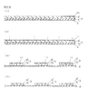
FIG. 1 is a cross section of a sealing member in an embodiment of the present invention. -
FIG. 2 is a process diagram for describing a method for producing the sealing member shown inFIG. 1 ,- (a) illustrating a step of forming a sealing resin layer on a base film, and
- (b) illustrating a step of forming a lens-forming resin layer on a releasing film.
-
FIG. 3 is, followingFIG. 2 , a process diagram for describing a method for producing a sealing member,- (c) illustrating a step of laminating a sealing resin layer and a lens-forming resin layer,
- (d) illustrating a step of forming a cut having a predetermined shape in the base film, the sealing resin layer, and the lens-forming resin layer,
- (e) illustrating a step of removing a portion excluding the cut having the predetermined shape of the base film, the sealing resin layer, and the lens-forming resin layer, and
- (f) a step of removing the base film.
-
FIG. 4 is a diagram for describing an embodiment of a sealing method of the present invention, illustrating a step of allowing a sealing member and an optical semiconductor element to face each other. -
FIG. 5 is a diagram for describing the sealing method shown inFIG. 4 , illustrating a step of sealing in an optical semiconductor element. -
FIG. 1 is a cross section of a sealing member in an embodiment of the present invention. - A
sealing member 1 includes, as shown inFIG. 1 , a releasingfilm 2; a plurality of sealinglayers 3 laminated on the releasingfilm 2; and aprotection film 4 laminated on the releasingfilm 2 so as to cover the sealinglayer 3. The sealingmember 1 is used, for example, for sealing in sealing objects such as optical semiconductor elements including a light-emitting element (ex. a light-emitting diode (LED)) and a light-receiving element. In this embodiment, description is given using an LED as an example of the sealing object. - The releasing
film 2 is formed into an elongated flat belt shape. - The sealing
layers 3 are formed into a generally circular shape when viewed from the top, and are arranged in a row along the longitudinal direction of the releasingfilm 2 with a space provided therebetween. The sealinglayer 3 includes a lens-formingresin layer 5 that is formed into a lens, and a sealingresin layer 6 that seals in an LED. - The lens-forming
resin layer 5 is transparent, formed into a generally circular shape when viewed from the top, and is laminated on the releasingfilm 2. - The sealing
resin layer 6 is transparent, formed into a generally circular shape when viewed from the top having about the same diameter with the lens-formingresin layer 5, and formed on the lens-formingresin layer 5 so as to share the center with the lens-formingresin layer 5. - That is, the lens-forming
resin layer 5 is interposed between the releasingfilm 2 and the sealingresin layer 6. - The
protection film 4 is formed into generally the same shape (elongated flat belt shape) as that of the releasingfilm 2. -
FIG. 2 andFIG. 3 are process diagrams for describing the method for producing a sealing member shown inFIG. 1 . - To produce the sealing
member 1, as shown inFIG. 2 (a) , first, the sealingresin layer 6 is formed on thebase film 11. - The
base film 11 is formed into an elongated flat belt shape from, for example, polyesters such as polyethylene terephthalate; and polyolefins such as polyethylene and polypropylene. - The
base film 11 has a thickness of, for example, 12 to 250 µm, or preferably 25 to 75 µm. - Examples of sealing resins that form the sealing
resin layer 6 include thermosetting resins such as thermosetting silicone resin, epoxy resin, thermosetting polyimide resin, phenolic resin, urea resin, melamine resin, unsaturated polyester resin, diallyl phthalate resin, and thermosetting urethane resin, and a preferable example is a thermosetting silicone resin. - To form the sealing
resin layer 6, a solution of the sealing resin is applied on thebase film 11, and dried, thereby producing a sealingresin layer 6 in a semi-cured state (B-STAGE). The solvent for dissolving the sealing resin is not particularly limited, and examples thereof include known organic solvents. - To allow the sealing
resin layer 6 to reach the B-STAGE, the sealingresin layer 6 is heated, for example, at 40 to 150°C for 1 to 60 min. - To cure the sealing
resin layer 6 completely, the sealingresin layer 6 is heated, for example, at 125 to 250°C for 5 minutes to 24 hours. - In the solution of the sealing resin, for example, phosphor particles and silica particles may be blended.
- Examples of phosphor particles include particles composed of a phosphor such as Y3Al5O12: Ce (YAG (yttrium ·aluminium garnet): Ce).
- The phosphor particles are blended at a proportion of, for example, 1 to 10 mass% relative to the total solid content in the solution of the sealing resin.
- Examples of silica particles include silica particles having an average particle size (volume-based, measured by dynamic light scattering method) of 20 nm or less.
- The silica particles are blended at a proportion of, for example, 5 to 20 mass% relative to the total solid content in the solution of the sealing resin.
- Examples of methods for applying the solution of the sealing resin onto the
base film 11 include methods using doctor blades, gravure coaters, and fountain coaters. - Although not limited, the solution of the sealing resin applied on the
base film 11 is dried, for example, at 100 to 150°C for 5 to 30 min. - The obtained sealing
resin layer 6 has a thickness of, for example, 300 to 500 µm, - To produce a sealing
member 1, as shown inFIG. 2 (b) , a lens-formingresin layer 5 is separately formed on the releasingfilm 2. - The releasing
film 2 is formed, for example, into an elongated flat belt shape from a fluorine resin such as ethylene-tetrafluoroethylene copolymer resin. - The releasing
film 2 has a thickness of, for example, 12 to 250 µm, or preferably 25 to 75 µm. - Examples of lens-forming resins that form the lens-forming
resin layer 5 include the above-described resins for the sealing resin. - To form the lens-forming
resin layer 5, in the same manner as the above-describedsealing resin layer 6, a lens-forming resin or a solution thereof is applied on the releasingfilm 2, and heated or dried, thereby producing a lens-formingresin layer 5 in a semi-cured state (B-STAGE). The solvent for dissolving the lens-forming resin is not particularly limited, and examples thereof include known organic solvents. - In the solution of the lens-forming resin, for example, the above-described silica particles may be blended.
- The silica particles are blended at a proportion of, for example, 5 to 20 mass% relative to the total solid content in the solution of the lens-forming resin.
- Examples of methods for applying the solution of the lens-forming resin onto the releasing
film 2 include methods using comma coaters, doctor blades, gravure coaters, and fountain coaters. - Although not limited, the solution of the lens-forming resin applied on the releasing
film 2 is dried, for example, by heating at 100 to 150°C for 5 to 30 main. - The obtained lens-forming
resin layer 5 has a thickness of, for example, 100 to 1200 µm, or preferably 600 to 900 µm. - Then, to produce a sealing
member 1, as shown inFIG. 3 (c) , the sealingresin layer 6 and the lens-formingresin layer 5 are bonded together, and pressed under normal temperature at a predetermined pressure. - This allows the sealing
resin layer 6 and the lens-formingresin layer 5 to be laminated, thereby forming asealing layer 3. - Then, as shown in
FIG. 3 (d) , using a circular die cutting blade, a plurality of generally circular cuts when viewed from the top are formed on thebase film 11 and the sealing layer 3 (the sealingresin layer 6 and the lens-forming resin layer 5) along the longitudinal direction of the releasingfilm 2 with a space provided therebetween; and as shown inFIG. 3 (e) , portions excluding the generally circular shape (when viewed from the top) portions of thebase film 11 and thesealing layer 3 are removed. - In this way, a plurality of sealing
layers 3 are formed along the longitudinal direction of the releasingfilm 2 with a space provided therebetween. - The
sealing layer 3 has a diameter of, for example, 50 to 300 mm, or preferably 100 to 200 mm. The sealing layers 3 are spaced apart by, for example, 20 to 1000 mm, or preferably 50 to 200 mm. - Then, as shown in
FIG. 3 (f) , after removing the remainedbase film 11, as shown inFIG. 1 , theprotection film 4 is laminated on the releasingfilm 2 so as to cover thesealing layer 3. - The
protection film 4 is formed, for example, into an elongated flat belt shape from polyolefins such as polyethylene and polypropylene. - The
protection film 4 has a thickness of, for example, 12 to 250 µm, or preferably 25 to 50 µm. - The sealing
member 1 is obtained in this manner. - The steps for producing the above-described
sealing member 1 are performed, industrially, by roll-to-roll processing. -
FIG. 4 andFIG. 5 are diagrams for describing an embodiment of a sealing method of the present invention. - Next, a method for producing an LED device using the obtained the sealing
member 1 to seal inLEDs 20 is described. In this method, as shown inFIG. 4 , using asealing device 21, while the sealingmember 1 is successively sent out, thesealing layer 3 and a light-emittingsubstrate 22 including theLEDs 20 are allowed to face each other, and theLEDs 20 are sealed in continuously. - In particular, the sealing
device 21 includes apressing unit 23, a sealingmember feed unit 24, a protectionfilm release unit 25, and a releasing film take-upunit 26. - The
pressing unit 23 includes abase portion 27 on which the light-emittingsubstrate 22 is placed; and ametal mold 28 that is disposed above and facing thebase portion 27 and that has a plurality of hemispherical depressions. Thepressing unit 23 presses, while heating, thesealing layer 3 and the light-emittingsubstrate 22 that are facing each other in a direction in which thesealing layer 3 and the light-emittingsubstrate 22 are brought closer. - The sealing
member feed unit 24 is disposed upstream with respect to thepressing unit 23 in the conveying direction of the sealingmember 1; retains the sealingmember 1 in a rolled state; and conveys the retained sealingmember 1 along the longitudinal direction of the sealingmember 1 towards the pressing unit 23 (between thebase portion 27 and the metal mold 28). - The protection
film release unit 25 is disposed between thepressing unit 23 and the sealingmember feed unit 24 in the conveying direction of the sealingmember 1, and peels off theprotection film 4 from the sealingmember 1 while winding the peeledprotection film 4 into a rolled state. - The releasing film take-up
unit 26 is disposed downstream with respect to thepressing unit 23 in the conveying direction of the sealingmember 1, and winds and takes up the used releasingfilm 2. - Then, to continuously seal in the
LEDs 20 using thesealing device 21, first, the light-emittingsubstrate 22 on which a plurality ofLEDs 20 are mounted is placed on thebase portion 27 of thepressing unit 23. At the same time, the sealingmember 1 is sent out from the sealingmember feed unit 24 towards a space between themetal mold 28 and the light-emittingsubstrate 22. - At this time, on the way from the sealing
member feed unit 24 to thepressing unit 23, theprotection film 4 is peeled off from the sealingmember 1 by the protectionfilm release unit 25, and the sealingresin layer 6 of thesealing layer 3 is exposed. - Then, the sealing
member 1 is successively sent out, thesealing layer 3 is disposed above the light-emittingsubstrate 22 on which theLEDs 20 are mounted so that the sealingresin layer 6 is exposed downward and the releasingfilm 2 faces themetal mold 28. The sealingresin layer 6 and theLEDs 20 are thus allowed to face each other vertically. - Then, while heating, the
metal mold 28 is brought closer to thebase portion 27, and, while heating, thesealing layer 3 is pressed against the light-emittingsubstrate 22. - The temperature of the
metal mold 28 is, for example, 120 to 200°C, or preferably 140 to 165°C. - The
base portion 27 is pressed against themetal mold 28 at, for example, 0.01 to 10 MPa, or preferably 0.1 to 4 MPa. - The
LEDs 20 are thus embedded in the sealingresin layer 6. In addition, the lens-formingresin layer 5 of thesealing layer 3 is injected into the depressions of themetal mold 28. At this time, the releasingfilm 2 is deformed so as to conform to the depressions of themetal mold 28, protecting the internal face of the depressions of themetal mold 28, and also allowing the entrance of the lens-formingresin layer 5 into the depressions of themetal mold 28. - Then, as shown in
FIG. 5 , by subsequently heating thesealing layer 3, the sealingresin layer 6 and the lens-formingresin layer 5 are completely cured. - Next, the
metal mold 28 is brought away upward from thebase portion 27 so as to be spaced apart therefrom, thereby opening the mold. This allows the releasingfilm 2 to be released from the depressions of themetal mold 28. - In this fashion, the
LEDs 20 are sealed in with the sealingresin layer 6, and at the same time, the lens-formingresin layer 5 is molded into lenses. - Next, while releasing the releasing
film 2 from the light-emittingsubstrate 22 in which theLEDs 20 are sealed in with thesealing layer 3, the light-emittingsubstrate 22 in which theLEDs 20 are sealed in with thesealing layer 3 is removed from thebase portion 27, and then a new light-emittingsubstrate 22 is placed on thebase portion 27. - At the same time, while winding up the peeled releasing
film 2 with the releasing film take-upunit 26, the sealingmember 1 is sent out from the sealingmember feed unit 24. - Then, as described above, a sealing
resin layer 6 andLEDs 20 are allowed to face each other vertically again. - In this way, the steps are repeated, i.e., the step of allowing the sealing
resin layer 6 and theLEDs 20 to face each other while conveying the sealingmember 1, and the step of pressing the sealingresin layer 6 facing theLEDs 20 towards and against theLEDs 20, thereby sealing in theLEDs 20 with the sealingresin layer 6. - In this way, using the
sealing device 21, theLEDs 20 can be sealed in continuously. - In this sealing method, as shown in
FIG. 4 , using the sealingmember 1 including the elongated releasingfilm 2 and the plurality of sealingresin layers 6 laminated on the releasingfilm 2 and arranged in a row along the longitudinal direction of the releasingfilm 2 with a space provided therebetween, the following is repeated: while conveying the sealingmember 1 in the longitudinal direction, the sealingresin layer 6 and theLEDs 20 are allowed to face each other, and the sealingresin layer 6 facing theLEDs 20 is pressed toward and against theLEDs 20, thereby sealing in theLEDs 20 with the sealingresin layer 6. - Therefore, the
LEDs 20 can be continuously sealed in by conveying the sealingmember 1 along the longitudinal direction, and successively sending out the sealingresin layers 6 together with the releasingfilm 2. - Therefore, when sealing in the
LEDs 20, the releasingfilm 2 and the sealingresin layer 6 can be set simultaneously every time, which allows shortening of time for re-setting the sealingresin layer 6. - As a result, the
LEDs 20 can be efficiently and continuously sealed in. - Furthermore, in this sealing method, the sealing
member 1 includes a lens-formingresin layer 5. - Thus, simultaneously with the sealing in of the
LEDs 20, lenses can be formed. - As a result, by using this sealing method to seal in the
LEDs 20, an LED device can be produced efficiently. - Although the sealing
resin layer 6 and the lens-formingresin layer 5 are set as thesealing layer 3 in the above-described sealing method, it is also possible to set only the sealingresin layer 6 as thesealing layer 3. - While the present invention is described in further detail with reference to Examples in the following, the present invention is not limited to any of them by no means.
- A thermosetting silicone resin containing 5 mass% of Y3Al5O12: Ce phosphor particles, and 10 mass% of silica particles having an average particle size (volume-based, measured by dynamic light scattering method) of 20 nm or less was applied on the releasing face of an elongated base film composed of polyethylene terephthalate and having a thickness of 50 µm, and heated at 120°C for 10 min, thereby producing a sealing resin layer (ref:
FIG. 2 (a) ) having a thickness of 400 µm in a semi-cured state (B-STAGE). - Separately, a thermosetting silicone resin containing 10 mass% of silica particles having an average particle size (volume-based, measured by dynamic light scattering method) of 20 nm or less was applied on an elongated releasing film composed of an ethylene-tetrafluoroethylene copolymer resin and having a thickness of 50 µm, and heated at 120°C for 10 min, thereby producing a lens-forming resin layer (ref:
FIG. 2 (b) ) having a thickness of 600 µm in a semi-cured state (B-STAGE). - Then, the obtained sealing resin layer and the lens-forming resin layer were bonded together, and a pressure was applied at a predetermined pressure and normal temperature, laminating the sealing resin layer and the lens-forming resin layer, thereby forming a sealing layer (ref:
FIG. 3 (c) ). - Then, a plurality of generally circular cuts having a diameter of 150 mm when viewed from the top were formed in the base film and the sealing layer (the sealing resin layer and the lens-forming resin layer) using a circular die cutting blade along the longitudinal direction of the releasing film with a distance of 150 mm provided therebetween (ref:
FIG. 3 (d) ), and portions of the base film and the sealing layer excluding the portions of the generally circular shape when viewed from the top were removed (ref:FIG. 3 (e) ). - In this way, a plurality of sealing layers having a generally circular shape when viewed from the top and having a diameter of 150 mm were formed along the longitudinal direction of the releasing film with a distance of 150 mm provided therebetween.
- Then, after removing the remaining base film (ref:
FIG. 3 (f) ), an elongated protection film composed of polypropylene was laminated on the releasing film so as to cover the sealing layer (ref:FIG. 1 ). - A sealing member was obtained in this manner.
- Using the sealing device shown in
FIG. 4 , while sending out the sealing member successively, the sealing layer, and a light-emitting substrate including the LEDs were allowed to face each other, and the LEDs were continuously sealed in. - Specifically, a light-emitting substrate on which a plurality of LEDs are mounted was placed on the base portion of the pressing unit. At the same time, the sealing member was sent out from the sealing member feed unit towards a space between the metal mold and the light-emitting substrate.
- At this time, on the way from the sealing member feed unit to the pressing unit, the protection film was peeled off by the protection film release unit from the sealing member, thereby exposing the sealing resin layer of the sealing layer.
- Thereafter, the sealing member was sent out, and the sealing layer was disposed above the light-emitting substrate on which LEDs were mounted so that the sealing resin layer was exposed downwardly and at the same time the releasing film faced the metal mold. The sealing resin layer and the LEDs were allowed to face each other vertically in this manner (ref:
FIG. 4 ). - Then, while heating at 160°C, the metal mold was brought closer to the base portion at an applied pressure of 2.77 MPa, and the sealing layer, while heating, was pressed against the light-emitting substrate.
- The LEDs were embedded in the sealing resin layer in this manner. Also, the lens-forming resin layer of the sealing layer was injected in the depressions of the metal mold.
- Subsequently, the sealing layer was heated, thereby completely curing the sealing resin layer and the lens-forming resin layer (ref:
FIG. 5 ). - Then, the metal mold was brought away upward so as to be spaced apart from the base portion, thereby opening the mold.
- In this fashion, the LEDs were sealed in with the sealing resin layer, and at the same time, the lens-forming resin layer was molded into a lens.
- Then, while peeling off the releasing film from the light-emitting substrate in which the LEDs were sealed in with the sealing layer, the light-emitting substrate in which the LEDs were sealed in with the sealing layer was removed from the base portion, and thereafter, a new light-emitting substrate was placed on the base portion.
- At the same time, while winding the peeled releasing film onto the releasing film take-up unit, the sealing member was sent out from the sealing member feed unit.
- The sealing resin layer and LEDs were allowed to face each other vertically again in this manner.
- As described above, while conveying the sealing member, the following steps were repeated: a step of allowing the sealing resin layer and LEDs to face each other, and a step of pressing the sealing resin layer facing the LEDs towards the LEDs, thereby sealing in the LEDs with the sealing resin layer.
- While the illustrative embodiments of the present invention are provided in the above description, such is for illustrative purpose only and it is not to be construed as limiting the scope of the present invention. Modifications and variations of the present invention that will be obvious to those skilled in the art are to be covered by the following claims.
Claims (6)
- A sealing member comprising:an elongated releasing film, anda plurality of sealing resin layers composed of a sealing resin, the plurality of sealing resin layers being laminated on the releasing film so that the plurality of sealing resin layers are arranged in a row along the longitudinal direction of the releasing film with a space provided therebetween.
- The sealing member according to Claim 1, wherein the sealing member seals in an optical semiconductor element.
- The sealing member according to Claim 2, further comprising a lens-forming resin layer composed of a lens-forming resin that forms a lens, and interposed between the releasing film and the sealing resin layer.
- The sealing member according to Claim 1, wherein the sealing resin is a thermosetting resin, and
the sealing resin layer is formed from the thermosetting resin in a B-stage state. - A sealing method comprising a repetition of the steps of:preparing a sealing member comprising an elongated releasing film, and a plurality of sealing resin layers composed of a sealing resin, the plurality of sealing resin layers being laminated on the releasing film so that the plurality of sealing resin layers are arranged in a row along the longitudinal direction of the releasing film with a space provided therebetween,allowing the sealing resin layer and a sealing object to face each other while conveying the sealing member in a longitudinal direction, andpressing the sealing resin layer and/or the sealing object that are facing each other in a direction such that the sealing resin layer and the sealing object are brought closer, so as to seal in the sealing object with the sealing resin layer.
- A sealing method according to claim 5, wherein the sealing object is an optical semiconductor element.
Applications Claiming Priority (1)
| Application Number | Priority Date | Filing Date | Title |
|---|---|---|---|
| JP2010292861A JP2012142364A (en) | 2010-12-28 | 2010-12-28 | Sealing member, sealing method, and manufacturing method of optical semiconductor device |
Publications (3)
| Publication Number | Publication Date |
|---|---|
| EP2472615A2 true EP2472615A2 (en) | 2012-07-04 |
| EP2472615A3 EP2472615A3 (en) | 2014-01-08 |
| EP2472615B1 EP2472615B1 (en) | 2016-04-20 |
Family
ID=45098947
Family Applications (1)
| Application Number | Title | Priority Date | Filing Date |
|---|---|---|---|
| EP11192972.5A Not-in-force EP2472615B1 (en) | 2010-12-28 | 2011-12-12 | Method for producing optical semiconductor device |
Country Status (6)
| Country | Link |
|---|---|
| US (2) | US20120160412A1 (en) |
| EP (1) | EP2472615B1 (en) |
| JP (1) | JP2012142364A (en) |
| KR (1) | KR20120075424A (en) |
| CN (1) | CN102543901A (en) |
| TW (1) | TW201251139A (en) |
Families Citing this family (11)
| Publication number | Priority date | Publication date | Assignee | Title |
|---|---|---|---|---|
| JP2014127525A (en) * | 2012-12-25 | 2014-07-07 | Shin Etsu Chem Co Ltd | Mold release film with sealing resin, sealing method of optical semiconductor element using the same, and optical semiconductor device including sealed optical semiconductor element |
| JP2014229791A (en) * | 2013-05-23 | 2014-12-08 | 日東電工株式会社 | Encapsulation sheet pasting method |
| WO2014188742A1 (en) * | 2013-05-24 | 2014-11-27 | 日東電工株式会社 | Sealing sheet and method for manufacturing same |
| CN106469767B (en) * | 2015-08-18 | 2017-12-01 | 江苏诚睿达光电有限公司 | A kind of change system of the organic siliconresin light conversion body fitting encapsulation LED based on series connection rolling |
| CN106469768B (en) * | 2015-08-18 | 2018-02-02 | 江苏诚睿达光电有限公司 | A kind of special-shaped organic siliconresin light conversion body fitting encapsulation LED change system |
| CN106469778B (en) * | 2015-08-18 | 2017-12-22 | 江苏诚睿达光电有限公司 | A kind of special-shaped organic siliconresin light conversion body fitting encapsulation LED process |
| CN106469780B (en) * | 2015-08-18 | 2018-02-13 | 江苏诚睿达光电有限公司 | A kind of process of the organic siliconresin light conversion body fitting encapsulation LED based on series connection rolling |
| JP6423399B2 (en) * | 2016-09-27 | 2018-11-14 | アピックヤマダ株式会社 | Resin molding method, film conveying apparatus, and resin molding apparatus |
| US11538777B2 (en) * | 2020-07-01 | 2022-12-27 | Sandisk Technologies Llc | Semiconductor structure containing pre-polymerized protective layer and method of making thereof |
| US11776922B2 (en) | 2020-07-01 | 2023-10-03 | Sandisk Technologies Llc | Semiconductor structure containing pre-polymerized protective layer and method of making thereof |
| KR102333673B1 (en) * | 2021-06-02 | 2021-12-02 | 넥스타테크놀로지 주식회사 | Apparatus for preparing semiconductor molding film |
Citations (1)
| Publication number | Priority date | Publication date | Assignee | Title |
|---|---|---|---|---|
| JP2002043345A (en) | 1998-07-10 | 2002-02-08 | Apic Yamada Corp | Method of manufacturing semiconductor device and resin- sealing device |
Family Cites Families (19)
| Publication number | Priority date | Publication date | Assignee | Title |
|---|---|---|---|---|
| JPH06163617A (en) * | 1992-11-21 | 1994-06-10 | Nitto Denko Corp | Semiconductor device sealing method |
| JPH07211738A (en) * | 1994-01-14 | 1995-08-11 | Nippon Chemicon Corp | Sealing of circuit element |
| JP2994219B2 (en) * | 1994-05-24 | 1999-12-27 | シャープ株式会社 | Method for manufacturing semiconductor device |
| US6881611B1 (en) * | 1996-07-12 | 2005-04-19 | Fujitsu Limited | Method and mold for manufacturing semiconductor device, semiconductor device and method for mounting the device |
| EP0971401B1 (en) * | 1998-07-10 | 2010-06-09 | Apic Yamada Corporation | Method of manufacturing semiconductor devices and a resin molding machine therefor |
| JP2002299699A (en) * | 2001-03-30 | 2002-10-11 | Sumitomo Electric Ind Ltd | Light emitting device and method of manufacturing the same |
| US7189601B2 (en) * | 2004-03-02 | 2007-03-13 | Texas Instruments Incorporated | System and method for forming mold caps over integrated circuit devices |
| JP2005294733A (en) * | 2004-04-05 | 2005-10-20 | Nitto Denko Corp | Optical semiconductor element sealing sheet and method for manufacturing optical semiconductor device using the sheet |
| DE102004041867A1 (en) * | 2004-08-27 | 2006-03-16 | Leonhard Kurz Gmbh & Co. Kg | Decorated injection molded article, as well as transfer film and method for producing such |
| JP4676735B2 (en) * | 2004-09-22 | 2011-04-27 | 東レ・ダウコーニング株式会社 | Optical semiconductor device manufacturing method and optical semiconductor device |
| JP2006140362A (en) * | 2004-11-15 | 2006-06-01 | Nitto Denko Corp | Optical semiconductor element sealing sheet and method for manufacturing optical semiconductor device using the sheet |
| JP2006323147A (en) * | 2005-05-19 | 2006-11-30 | Seiko Epson Corp | Microlens manufacturing method, microlens, optical film, projection screen, projector system, electro-optical device, and electronic apparatus |
| US7985357B2 (en) * | 2005-07-12 | 2011-07-26 | Towa Corporation | Method of resin-sealing and molding an optical device |
| US8048358B2 (en) * | 2006-04-18 | 2011-11-01 | Texas Instruments Incorporated | Pop semiconductor device manufacturing method |
| JP2008230114A (en) * | 2007-03-22 | 2008-10-02 | Hitachi Chem Co Ltd | Sealing film |
| JP2009137253A (en) * | 2007-12-10 | 2009-06-25 | Dainippon Printing Co Ltd | Method for forming protective layer using thermal transfer sheet |
| JP2010159411A (en) * | 2008-12-12 | 2010-07-22 | Nitto Denko Corp | Semi-cured silicone resin sheet |
| JP5566088B2 (en) * | 2008-12-12 | 2014-08-06 | 日東電工株式会社 | Composition for thermosetting silicone resin |
| JP4913858B2 (en) * | 2009-04-14 | 2012-04-11 | 日東電工株式会社 | Composition for thermosetting silicone resin |
-
2010
- 2010-12-28 JP JP2010292861A patent/JP2012142364A/en active Pending
-
2011
- 2011-12-07 CN CN2011104050576A patent/CN102543901A/en active Pending
- 2011-12-12 TW TW100145830A patent/TW201251139A/en unknown
- 2011-12-12 EP EP11192972.5A patent/EP2472615B1/en not_active Not-in-force
- 2011-12-20 US US13/331,219 patent/US20120160412A1/en not_active Abandoned
- 2011-12-27 KR KR1020110143426A patent/KR20120075424A/en not_active Withdrawn
-
2014
- 2014-03-14 US US14/211,291 patent/US20140199795A1/en not_active Abandoned
Patent Citations (1)
| Publication number | Priority date | Publication date | Assignee | Title |
|---|---|---|---|---|
| JP2002043345A (en) | 1998-07-10 | 2002-02-08 | Apic Yamada Corp | Method of manufacturing semiconductor device and resin- sealing device |
Also Published As
| Publication number | Publication date |
|---|---|
| CN102543901A (en) | 2012-07-04 |
| EP2472615A3 (en) | 2014-01-08 |
| US20140199795A1 (en) | 2014-07-17 |
| KR20120075424A (en) | 2012-07-06 |
| TW201251139A (en) | 2012-12-16 |
| JP2012142364A (en) | 2012-07-26 |
| EP2472615B1 (en) | 2016-04-20 |
| US20120160412A1 (en) | 2012-06-28 |
Similar Documents
| Publication | Publication Date | Title |
|---|---|---|
| EP2472615B1 (en) | Method for producing optical semiconductor device | |
| KR101253586B1 (en) | Phosphor film, method of manufacturing the same, method of coating phosphor layer on an LED chip, method of manufacturing LED package and LED package manufactured thereof | |
| US11024781B2 (en) | Glueless light emitting device with phosphor converter | |
| CN1174479C (en) | Manufacturing method of semiconductor device | |
| EP2680327A2 (en) | Reflecting layer-phosphor layer-covered LED, producing method thereof, LED device, and producing method thereof | |
| EP2680328A2 (en) | Phosphor layer-covered LED, producing method thereof, and LED device | |
| US20100283065A1 (en) | Led device with a light extracting rough structure and manufacturing methods thereof | |
| KR20170128298A (en) | Optical semiconductor element with light reflecting layer and method for manufacturing optical semiconductor element with light reflecting layer and phosphor layer | |
| JP2014168036A (en) | Sealing layer covered semiconductor element, manufacturing method of the same, and semiconductor device | |
| KR101849447B1 (en) | Semiconductor device using singulated unit substrate and manufacturing method thereof | |
| JP2014165462A (en) | Semiconductor chip manufacturing method | |
| EP2680330A2 (en) | Encapsulating layer-covered semiconductor element, producing method thereof, and semiconductor device | |
| JP2009051107A (en) | Optical element resin sealing molding method and apparatus | |
| JP5800640B2 (en) | Method for manufacturing light emitting diode device | |
| EP3188261B1 (en) | Chip scale packaging light emitting device and manufacturing method of the same | |
| US20180033925A1 (en) | Method of producing a light-emitting device, and light-emitting device | |
| CN103715329A (en) | High-power LED chip making method | |
| CN1171173C (en) | Manufacturing method of non-contact data carrier | |
| US11398587B2 (en) | Method of manufacturing light-transmissive sheet | |
| JP2018523256A (en) | Conversion part manufacturing method and optoelectronic lighting device | |
| KR101364438B1 (en) | Manufacturing method of semiconductor device using a energy ray -responsive heat-resistant adhesive sheet | |
| US10879427B2 (en) | Method of producing an optoelectronic component, and optoelectronic component | |
| KR101132346B1 (en) | Adhesive resin composition for fan-out wafer level package and adhesive tape using the same | |
| JP5359732B2 (en) | Method for manufacturing light emitting device | |
| JP2019033175A (en) | Manufacturing method of semiconductor device |
Legal Events
| Date | Code | Title | Description |
|---|---|---|---|
| AK | Designated contracting states |
Kind code of ref document: A2 Designated state(s): AL AT BE BG CH CY CZ DE DK EE ES FI FR GB GR HR HU IE IS IT LI LT LU LV MC MK MT NL NO PL PT RO RS SE SI SK SM TR |
|
| AX | Request for extension of the european patent |
Extension state: BA ME |
|
| PUAI | Public reference made under article 153(3) epc to a published international application that has entered the european phase |
Free format text: ORIGINAL CODE: 0009012 |
|
| RIN1 | Information on inventor provided before grant (corrected) |
Inventor name: ITO, HISATAKA Inventor name: SHINBORI, YUKI Inventor name: OOYABU, YASUNARI Inventor name: SATO, SATOSHI |
|
| PUAL | Search report despatched |
Free format text: ORIGINAL CODE: 0009013 |
|
| AK | Designated contracting states |
Kind code of ref document: A3 Designated state(s): AL AT BE BG CH CY CZ DE DK EE ES FI FR GB GR HR HU IE IS IT LI LT LU LV MC MK MT NL NO PL PT RO RS SE SI SK SM TR |
|
| AX | Request for extension of the european patent |
Extension state: BA ME |
|
| RIC1 | Information provided on ipc code assigned before grant |
Ipc: B29C 43/20 20060101ALI20131129BHEP Ipc: H01L 33/52 20100101AFI20131129BHEP Ipc: B29C 43/18 20060101ALI20131129BHEP |
|
| 17P | Request for examination filed |
Effective date: 20140624 |
|
| RBV | Designated contracting states (corrected) |
Designated state(s): AL AT BE BG CH CY CZ DE DK EE ES FI FR GB GR HR HU IE IS IT LI LT LU LV MC MK MT NL NO PL PT RO RS SE SI SK SM TR |
|
| GRAP | Despatch of communication of intention to grant a patent |
Free format text: ORIGINAL CODE: EPIDOSNIGR1 |
|
| INTG | Intention to grant announced |
Effective date: 20151208 |
|
| GRAS | Grant fee paid |
Free format text: ORIGINAL CODE: EPIDOSNIGR3 |
|
| GRAA | (expected) grant |
Free format text: ORIGINAL CODE: 0009210 |
|
| AK | Designated contracting states |
Kind code of ref document: B1 Designated state(s): AL AT BE BG CH CY CZ DE DK EE ES FI FR GB GR HR HU IE IS IT LI LT LU LV MC MK MT NL NO PL PT RO RS SE SI SK SM TR |
|
| REG | Reference to a national code |
Ref country code: GB Ref legal event code: FG4D |
|
| REG | Reference to a national code |
Ref country code: CH Ref legal event code: EP |
|
| REG | Reference to a national code |
Ref country code: AT Ref legal event code: REF Ref document number: 793281 Country of ref document: AT Kind code of ref document: T Effective date: 20160515 |
|
| REG | Reference to a national code |
Ref country code: IE Ref legal event code: FG4D |
|
| REG | Reference to a national code |
Ref country code: DE Ref legal event code: R096 Ref document number: 602011025501 Country of ref document: DE |
|
| REG | Reference to a national code |
Ref country code: LT Ref legal event code: MG4D |
|
| REG | Reference to a national code |
Ref country code: AT Ref legal event code: MK05 Ref document number: 793281 Country of ref document: AT Kind code of ref document: T Effective date: 20160420 |
|
| REG | Reference to a national code |
Ref country code: NL Ref legal event code: MP Effective date: 20160420 |
|
| PG25 | Lapsed in a contracting state [announced via postgrant information from national office to epo] |
Ref country code: PL Free format text: LAPSE BECAUSE OF FAILURE TO SUBMIT A TRANSLATION OF THE DESCRIPTION OR TO PAY THE FEE WITHIN THE PRESCRIBED TIME-LIMIT Effective date: 20160420 Ref country code: NO Free format text: LAPSE BECAUSE OF FAILURE TO SUBMIT A TRANSLATION OF THE DESCRIPTION OR TO PAY THE FEE WITHIN THE PRESCRIBED TIME-LIMIT Effective date: 20160720 Ref country code: LT Free format text: LAPSE BECAUSE OF FAILURE TO SUBMIT A TRANSLATION OF THE DESCRIPTION OR TO PAY THE FEE WITHIN THE PRESCRIBED TIME-LIMIT Effective date: 20160420 Ref country code: NL Free format text: LAPSE BECAUSE OF FAILURE TO SUBMIT A TRANSLATION OF THE DESCRIPTION OR TO PAY THE FEE WITHIN THE PRESCRIBED TIME-LIMIT Effective date: 20160420 Ref country code: FI Free format text: LAPSE BECAUSE OF FAILURE TO SUBMIT A TRANSLATION OF THE DESCRIPTION OR TO PAY THE FEE WITHIN THE PRESCRIBED TIME-LIMIT Effective date: 20160420 |
|
| PG25 | Lapsed in a contracting state [announced via postgrant information from national office to epo] |
Ref country code: RS Free format text: LAPSE BECAUSE OF FAILURE TO SUBMIT A TRANSLATION OF THE DESCRIPTION OR TO PAY THE FEE WITHIN THE PRESCRIBED TIME-LIMIT Effective date: 20160420 Ref country code: LV Free format text: LAPSE BECAUSE OF FAILURE TO SUBMIT A TRANSLATION OF THE DESCRIPTION OR TO PAY THE FEE WITHIN THE PRESCRIBED TIME-LIMIT Effective date: 20160420 Ref country code: SE Free format text: LAPSE BECAUSE OF FAILURE TO SUBMIT A TRANSLATION OF THE DESCRIPTION OR TO PAY THE FEE WITHIN THE PRESCRIBED TIME-LIMIT Effective date: 20160420 Ref country code: HR Free format text: LAPSE BECAUSE OF FAILURE TO SUBMIT A TRANSLATION OF THE DESCRIPTION OR TO PAY THE FEE WITHIN THE PRESCRIBED TIME-LIMIT Effective date: 20160420 Ref country code: GR Free format text: LAPSE BECAUSE OF FAILURE TO SUBMIT A TRANSLATION OF THE DESCRIPTION OR TO PAY THE FEE WITHIN THE PRESCRIBED TIME-LIMIT Effective date: 20160721 Ref country code: AT Free format text: LAPSE BECAUSE OF FAILURE TO SUBMIT A TRANSLATION OF THE DESCRIPTION OR TO PAY THE FEE WITHIN THE PRESCRIBED TIME-LIMIT Effective date: 20160420 Ref country code: PT Free format text: LAPSE BECAUSE OF FAILURE TO SUBMIT A TRANSLATION OF THE DESCRIPTION OR TO PAY THE FEE WITHIN THE PRESCRIBED TIME-LIMIT Effective date: 20160822 Ref country code: ES Free format text: LAPSE BECAUSE OF FAILURE TO SUBMIT A TRANSLATION OF THE DESCRIPTION OR TO PAY THE FEE WITHIN THE PRESCRIBED TIME-LIMIT Effective date: 20160420 |
|
| PG25 | Lapsed in a contracting state [announced via postgrant information from national office to epo] |
Ref country code: IT Free format text: LAPSE BECAUSE OF FAILURE TO SUBMIT A TRANSLATION OF THE DESCRIPTION OR TO PAY THE FEE WITHIN THE PRESCRIBED TIME-LIMIT Effective date: 20160420 Ref country code: BE Free format text: LAPSE BECAUSE OF FAILURE TO SUBMIT A TRANSLATION OF THE DESCRIPTION OR TO PAY THE FEE WITHIN THE PRESCRIBED TIME-LIMIT Effective date: 20160420 |
|
| REG | Reference to a national code |
Ref country code: DE Ref legal event code: R097 Ref document number: 602011025501 Country of ref document: DE |
|
| PG25 | Lapsed in a contracting state [announced via postgrant information from national office to epo] |
Ref country code: CZ Free format text: LAPSE BECAUSE OF FAILURE TO SUBMIT A TRANSLATION OF THE DESCRIPTION OR TO PAY THE FEE WITHIN THE PRESCRIBED TIME-LIMIT Effective date: 20160420 Ref country code: DK Free format text: LAPSE BECAUSE OF FAILURE TO SUBMIT A TRANSLATION OF THE DESCRIPTION OR TO PAY THE FEE WITHIN THE PRESCRIBED TIME-LIMIT Effective date: 20160420 Ref country code: EE Free format text: LAPSE BECAUSE OF FAILURE TO SUBMIT A TRANSLATION OF THE DESCRIPTION OR TO PAY THE FEE WITHIN THE PRESCRIBED TIME-LIMIT Effective date: 20160420 Ref country code: SK Free format text: LAPSE BECAUSE OF FAILURE TO SUBMIT A TRANSLATION OF THE DESCRIPTION OR TO PAY THE FEE WITHIN THE PRESCRIBED TIME-LIMIT Effective date: 20160420 Ref country code: RO Free format text: LAPSE BECAUSE OF FAILURE TO SUBMIT A TRANSLATION OF THE DESCRIPTION OR TO PAY THE FEE WITHIN THE PRESCRIBED TIME-LIMIT Effective date: 20160420 |
|
| PLBE | No opposition filed within time limit |
Free format text: ORIGINAL CODE: 0009261 |
|
| STAA | Information on the status of an ep patent application or granted ep patent |
Free format text: STATUS: NO OPPOSITION FILED WITHIN TIME LIMIT |
|
| PG25 | Lapsed in a contracting state [announced via postgrant information from national office to epo] |
Ref country code: SM Free format text: LAPSE BECAUSE OF FAILURE TO SUBMIT A TRANSLATION OF THE DESCRIPTION OR TO PAY THE FEE WITHIN THE PRESCRIBED TIME-LIMIT Effective date: 20160420 |
|
| 26N | No opposition filed |
Effective date: 20170123 |
|
| PG25 | Lapsed in a contracting state [announced via postgrant information from national office to epo] |
Ref country code: SI Free format text: LAPSE BECAUSE OF FAILURE TO SUBMIT A TRANSLATION OF THE DESCRIPTION OR TO PAY THE FEE WITHIN THE PRESCRIBED TIME-LIMIT Effective date: 20160420 |
|
| REG | Reference to a national code |
Ref country code: DE Ref legal event code: R119 Ref document number: 602011025501 Country of ref document: DE |
|
| REG | Reference to a national code |
Ref country code: CH Ref legal event code: PL |
|
| GBPC | Gb: european patent ceased through non-payment of renewal fee |
Effective date: 20161212 |
|
| PG25 | Lapsed in a contracting state [announced via postgrant information from national office to epo] |
Ref country code: MC Free format text: LAPSE BECAUSE OF FAILURE TO SUBMIT A TRANSLATION OF THE DESCRIPTION OR TO PAY THE FEE WITHIN THE PRESCRIBED TIME-LIMIT Effective date: 20160420 |
|
| REG | Reference to a national code |
Ref country code: FR Ref legal event code: ST Effective date: 20170831 |
|
| REG | Reference to a national code |
Ref country code: IE Ref legal event code: MM4A |
|
| PG25 | Lapsed in a contracting state [announced via postgrant information from national office to epo] |
Ref country code: FR Free format text: LAPSE BECAUSE OF NON-PAYMENT OF DUE FEES Effective date: 20170102 Ref country code: CH Free format text: LAPSE BECAUSE OF NON-PAYMENT OF DUE FEES Effective date: 20161231 Ref country code: LI Free format text: LAPSE BECAUSE OF NON-PAYMENT OF DUE FEES Effective date: 20161231 Ref country code: LU Free format text: LAPSE BECAUSE OF NON-PAYMENT OF DUE FEES Effective date: 20161212 |
|
| PG25 | Lapsed in a contracting state [announced via postgrant information from national office to epo] |
Ref country code: DE Free format text: LAPSE BECAUSE OF NON-PAYMENT OF DUE FEES Effective date: 20170701 Ref country code: IE Free format text: LAPSE BECAUSE OF NON-PAYMENT OF DUE FEES Effective date: 20161212 Ref country code: GB Free format text: LAPSE BECAUSE OF NON-PAYMENT OF DUE FEES Effective date: 20161212 |
|
| PG25 | Lapsed in a contracting state [announced via postgrant information from national office to epo] |
Ref country code: HU Free format text: LAPSE BECAUSE OF FAILURE TO SUBMIT A TRANSLATION OF THE DESCRIPTION OR TO PAY THE FEE WITHIN THE PRESCRIBED TIME-LIMIT; INVALID AB INITIO Effective date: 20111212 Ref country code: CY Free format text: LAPSE BECAUSE OF FAILURE TO SUBMIT A TRANSLATION OF THE DESCRIPTION OR TO PAY THE FEE WITHIN THE PRESCRIBED TIME-LIMIT Effective date: 20160420 |
|
| PG25 | Lapsed in a contracting state [announced via postgrant information from national office to epo] |
Ref country code: MK Free format text: LAPSE BECAUSE OF FAILURE TO SUBMIT A TRANSLATION OF THE DESCRIPTION OR TO PAY THE FEE WITHIN THE PRESCRIBED TIME-LIMIT Effective date: 20160420 Ref country code: IS Free format text: LAPSE BECAUSE OF FAILURE TO SUBMIT A TRANSLATION OF THE DESCRIPTION OR TO PAY THE FEE WITHIN THE PRESCRIBED TIME-LIMIT Effective date: 20160420 Ref country code: TR Free format text: LAPSE BECAUSE OF FAILURE TO SUBMIT A TRANSLATION OF THE DESCRIPTION OR TO PAY THE FEE WITHIN THE PRESCRIBED TIME-LIMIT Effective date: 20160420 |
|
| PG25 | Lapsed in a contracting state [announced via postgrant information from national office to epo] |
Ref country code: BG Free format text: LAPSE BECAUSE OF FAILURE TO SUBMIT A TRANSLATION OF THE DESCRIPTION OR TO PAY THE FEE WITHIN THE PRESCRIBED TIME-LIMIT Effective date: 20160420 |
|
| PG25 | Lapsed in a contracting state [announced via postgrant information from national office to epo] |
Ref country code: MT Free format text: LAPSE BECAUSE OF NON-PAYMENT OF DUE FEES Effective date: 20161212 |
|
| PG25 | Lapsed in a contracting state [announced via postgrant information from national office to epo] |
Ref country code: AL Free format text: LAPSE BECAUSE OF FAILURE TO SUBMIT A TRANSLATION OF THE DESCRIPTION OR TO PAY THE FEE WITHIN THE PRESCRIBED TIME-LIMIT Effective date: 20160420 |