EP2472590A2 - Electrode, photovoltaic device, and method of making - Google Patents
Electrode, photovoltaic device, and method of making Download PDFInfo
- Publication number
- EP2472590A2 EP2472590A2 EP20110190195 EP11190195A EP2472590A2 EP 2472590 A2 EP2472590 A2 EP 2472590A2 EP 20110190195 EP20110190195 EP 20110190195 EP 11190195 A EP11190195 A EP 11190195A EP 2472590 A2 EP2472590 A2 EP 2472590A2
- Authority
- EP
- European Patent Office
- Prior art keywords
- region
- cadmium
- layer
- tin
- tin oxide
- Prior art date
- Legal status (The legal status is an assumption and is not a legal conclusion. Google has not performed a legal analysis and makes no representation as to the accuracy of the status listed.)
- Withdrawn
Links
- 238000004519 manufacturing process Methods 0.000 title abstract description 13
- BEQNOZDXPONEMR-UHFFFAOYSA-N cadmium;oxotin Chemical compound [Cd].[Sn]=O BEQNOZDXPONEMR-UHFFFAOYSA-N 0.000 claims abstract description 120
- 229910052793 cadmium Inorganic materials 0.000 claims abstract description 110
- BDOSMKKIYDKNTQ-UHFFFAOYSA-N cadmium atom Chemical compound [Cd] BDOSMKKIYDKNTQ-UHFFFAOYSA-N 0.000 claims abstract description 109
- ATJFFYVFTNAWJD-UHFFFAOYSA-N Tin Chemical compound [Sn] ATJFFYVFTNAWJD-UHFFFAOYSA-N 0.000 claims abstract description 87
- 229910052718 tin Inorganic materials 0.000 claims abstract description 77
- 230000007704 transition Effects 0.000 claims abstract description 59
- 239000000758 substrate Substances 0.000 claims abstract description 51
- QVGXLLKOCUKJST-UHFFFAOYSA-N atomic oxygen Chemical compound [O] QVGXLLKOCUKJST-UHFFFAOYSA-N 0.000 claims abstract description 31
- 229910052760 oxygen Inorganic materials 0.000 claims abstract description 31
- 239000001301 oxygen Substances 0.000 claims abstract description 31
- 239000004065 semiconductor Substances 0.000 claims description 61
- WUPHOULIZUERAE-UHFFFAOYSA-N 3-(oxolan-2-yl)propanoic acid Chemical compound OC(=O)CCC1CCCO1 WUPHOULIZUERAE-UHFFFAOYSA-N 0.000 claims description 40
- 229910052980 cadmium sulfide Inorganic materials 0.000 claims description 40
- 238000000034 method Methods 0.000 claims description 24
- MARUHZGHZWCEQU-UHFFFAOYSA-N 5-phenyl-2h-tetrazole Chemical compound C1=CC=CC=C1C1=NNN=N1 MARUHZGHZWCEQU-UHFFFAOYSA-N 0.000 claims description 18
- 238000010438 heat treatment Methods 0.000 claims description 12
- 230000015572 biosynthetic process Effects 0.000 claims description 8
- 239000013078 crystal Substances 0.000 claims description 5
- 239000011029 spinel Substances 0.000 claims description 5
- 229910052596 spinel Inorganic materials 0.000 claims description 5
- 230000007423 decrease Effects 0.000 claims description 4
- 239000010410 layer Substances 0.000 description 295
- 239000010408 film Substances 0.000 description 30
- 238000000137 annealing Methods 0.000 description 25
- XOLBLPGZBRYERU-UHFFFAOYSA-N tin dioxide Chemical compound O=[Sn]=O XOLBLPGZBRYERU-UHFFFAOYSA-N 0.000 description 22
- 229910001887 tin oxide Inorganic materials 0.000 description 21
- XKRFYHLGVUSROY-UHFFFAOYSA-N Argon Chemical compound [Ar] XKRFYHLGVUSROY-UHFFFAOYSA-N 0.000 description 20
- 230000003287 optical effect Effects 0.000 description 17
- 239000000203 mixture Substances 0.000 description 16
- 230000006870 function Effects 0.000 description 13
- 238000004544 sputter deposition Methods 0.000 description 12
- 238000000151 deposition Methods 0.000 description 11
- 239000000463 material Substances 0.000 description 11
- 229910052786 argon Inorganic materials 0.000 description 10
- 230000005540 biological transmission Effects 0.000 description 9
- 239000010409 thin film Substances 0.000 description 9
- 239000007789 gas Substances 0.000 description 8
- 239000011521 glass Substances 0.000 description 8
- XLOMVQKBTHCTTD-UHFFFAOYSA-N Zinc monoxide Chemical compound [Zn]=O XLOMVQKBTHCTTD-UHFFFAOYSA-N 0.000 description 6
- 239000006096 absorbing agent Substances 0.000 description 6
- 238000002441 X-ray diffraction Methods 0.000 description 5
- 239000011149 active material Substances 0.000 description 5
- 238000001000 micrograph Methods 0.000 description 5
- 230000005855 radiation Effects 0.000 description 5
- 238000005477 sputtering target Methods 0.000 description 5
- 238000000859 sublimation Methods 0.000 description 5
- 230000008022 sublimation Effects 0.000 description 5
- SKJCKYVIQGBWTN-UHFFFAOYSA-N (4-hydroxyphenyl) methanesulfonate Chemical compound CS(=O)(=O)OC1=CC=C(O)C=C1 SKJCKYVIQGBWTN-UHFFFAOYSA-N 0.000 description 4
- RYGMFSIKBFXOCR-UHFFFAOYSA-N Copper Chemical compound [Cu] RYGMFSIKBFXOCR-UHFFFAOYSA-N 0.000 description 4
- 229910052802 copper Inorganic materials 0.000 description 4
- 239000010949 copper Substances 0.000 description 4
- 230000007547 defect Effects 0.000 description 4
- 229910052751 metal Inorganic materials 0.000 description 4
- 239000002184 metal Substances 0.000 description 4
- 230000008569 process Effects 0.000 description 4
- VYPSYNLAJGMNEJ-UHFFFAOYSA-N Silicium dioxide Chemical compound O=[Si]=O VYPSYNLAJGMNEJ-UHFFFAOYSA-N 0.000 description 3
- 238000002425 crystallisation Methods 0.000 description 3
- 230000008025 crystallization Effects 0.000 description 3
- 239000002019 doping agent Substances 0.000 description 3
- 230000000694 effects Effects 0.000 description 3
- 229910052738 indium Inorganic materials 0.000 description 3
- APFVFJFRJDLVQX-UHFFFAOYSA-N indium atom Chemical compound [In] APFVFJFRJDLVQX-UHFFFAOYSA-N 0.000 description 3
- 229910003437 indium oxide Inorganic materials 0.000 description 3
- PJXISJQVUVHSOJ-UHFFFAOYSA-N indium(iii) oxide Chemical compound [O-2].[O-2].[O-2].[In+3].[In+3] PJXISJQVUVHSOJ-UHFFFAOYSA-N 0.000 description 3
- 239000011787 zinc oxide Substances 0.000 description 3
- PXHVJJICTQNCMI-UHFFFAOYSA-N Nickel Chemical compound [Ni] PXHVJJICTQNCMI-UHFFFAOYSA-N 0.000 description 2
- KDLHZDBZIXYQEI-UHFFFAOYSA-N Palladium Chemical compound [Pd] KDLHZDBZIXYQEI-UHFFFAOYSA-N 0.000 description 2
- HCHKCACWOHOZIP-UHFFFAOYSA-N Zinc Chemical compound [Zn] HCHKCACWOHOZIP-UHFFFAOYSA-N 0.000 description 2
- YKYOUMDCQGMQQO-UHFFFAOYSA-L cadmium dichloride Chemical compound Cl[Cd]Cl YKYOUMDCQGMQQO-UHFFFAOYSA-L 0.000 description 2
- CXKCTMHTOKXKQT-UHFFFAOYSA-N cadmium oxide Inorganic materials [Cd]=O CXKCTMHTOKXKQT-UHFFFAOYSA-N 0.000 description 2
- QWUZMTJBRUASOW-UHFFFAOYSA-N cadmium tellanylidenezinc Chemical compound [Zn].[Cd].[Te] QWUZMTJBRUASOW-UHFFFAOYSA-N 0.000 description 2
- CFEAAQFZALKQPA-UHFFFAOYSA-N cadmium(2+);oxygen(2-) Chemical compound [O-2].[Cd+2] CFEAAQFZALKQPA-UHFFFAOYSA-N 0.000 description 2
- 230000008859 change Effects 0.000 description 2
- 238000003618 dip coating Methods 0.000 description 2
- -1 for example Substances 0.000 description 2
- AMGQUBHHOARCQH-UHFFFAOYSA-N indium;oxotin Chemical compound [In].[Sn]=O AMGQUBHHOARCQH-UHFFFAOYSA-N 0.000 description 2
- BASFCYQUMIYNBI-UHFFFAOYSA-N platinum Chemical compound [Pt] BASFCYQUMIYNBI-UHFFFAOYSA-N 0.000 description 2
- 238000005086 pumping Methods 0.000 description 2
- 238000005546 reactive sputtering Methods 0.000 description 2
- 238000004626 scanning electron microscopy Methods 0.000 description 2
- 238000004528 spin coating Methods 0.000 description 2
- 238000005507 spraying Methods 0.000 description 2
- 239000000126 substance Substances 0.000 description 2
- XSOKHXFFCGXDJZ-UHFFFAOYSA-N telluride(2-) Chemical compound [Te-2] XSOKHXFFCGXDJZ-UHFFFAOYSA-N 0.000 description 2
- 229910052725 zinc Inorganic materials 0.000 description 2
- 239000011701 zinc Substances 0.000 description 2
- OYPRJOBELJOOCE-UHFFFAOYSA-N Calcium Chemical compound [Ca] OYPRJOBELJOOCE-UHFFFAOYSA-N 0.000 description 1
- GYHNNYVSQQEPJS-UHFFFAOYSA-N Gallium Chemical compound [Ga] GYHNNYVSQQEPJS-UHFFFAOYSA-N 0.000 description 1
- FYYHWMGAXLPEAU-UHFFFAOYSA-N Magnesium Chemical compound [Mg] FYYHWMGAXLPEAU-UHFFFAOYSA-N 0.000 description 1
- ZOKXTWBITQBERF-UHFFFAOYSA-N Molybdenum Chemical compound [Mo] ZOKXTWBITQBERF-UHFFFAOYSA-N 0.000 description 1
- KJTLSVCANCCWHF-UHFFFAOYSA-N Ruthenium Chemical compound [Ru] KJTLSVCANCCWHF-UHFFFAOYSA-N 0.000 description 1
- BUGBHKTXTAQXES-UHFFFAOYSA-N Selenium Chemical compound [Se] BUGBHKTXTAQXES-UHFFFAOYSA-N 0.000 description 1
- NINIDFKCEFEMDL-UHFFFAOYSA-N Sulfur Chemical compound [S] NINIDFKCEFEMDL-UHFFFAOYSA-N 0.000 description 1
- 239000005864 Sulphur Substances 0.000 description 1
- RTAQQCXQSZGOHL-UHFFFAOYSA-N Titanium Chemical compound [Ti] RTAQQCXQSZGOHL-UHFFFAOYSA-N 0.000 description 1
- QCWXUUIWCKQGHC-UHFFFAOYSA-N Zirconium Chemical compound [Zr] QCWXUUIWCKQGHC-UHFFFAOYSA-N 0.000 description 1
- QDOSJNSYIUHXQG-UHFFFAOYSA-N [Mn].[Cd] Chemical compound [Mn].[Cd] QDOSJNSYIUHXQG-UHFFFAOYSA-N 0.000 description 1
- 238000010521 absorption reaction Methods 0.000 description 1
- 230000003466 anti-cipated effect Effects 0.000 description 1
- 239000005388 borosilicate glass Substances 0.000 description 1
- 229940065285 cadmium compound Drugs 0.000 description 1
- 150000001662 cadmium compounds Chemical class 0.000 description 1
- WZGKIRHYWDCEKP-UHFFFAOYSA-N cadmium magnesium Chemical compound [Mg].[Cd] WZGKIRHYWDCEKP-UHFFFAOYSA-N 0.000 description 1
- CJOBVZJTOIVNNF-UHFFFAOYSA-N cadmium sulfide Chemical compound [Cd]=S CJOBVZJTOIVNNF-UHFFFAOYSA-N 0.000 description 1
- 229910052791 calcium Inorganic materials 0.000 description 1
- 239000011575 calcium Substances 0.000 description 1
- 239000000969 carrier Substances 0.000 description 1
- 239000000919 ceramic Substances 0.000 description 1
- 238000006243 chemical reaction Methods 0.000 description 1
- 239000007795 chemical reaction product Substances 0.000 description 1
- 230000000295 complement effect Effects 0.000 description 1
- 238000005336 cracking Methods 0.000 description 1
- 230000003247 decreasing effect Effects 0.000 description 1
- 238000007598 dipping method Methods 0.000 description 1
- 230000005670 electromagnetic radiation Effects 0.000 description 1
- 238000005516 engineering process Methods 0.000 description 1
- 229910052733 gallium Inorganic materials 0.000 description 1
- PCHJSUWPFVWCPO-UHFFFAOYSA-N gold Chemical compound [Au] PCHJSUWPFVWCPO-UHFFFAOYSA-N 0.000 description 1
- 229910052737 gold Inorganic materials 0.000 description 1
- 239000010931 gold Substances 0.000 description 1
- 229910052735 hafnium Inorganic materials 0.000 description 1
- VBJZVLUMGGDVMO-UHFFFAOYSA-N hafnium atom Chemical compound [Hf] VBJZVLUMGGDVMO-UHFFFAOYSA-N 0.000 description 1
- 239000012535 impurity Substances 0.000 description 1
- 238000011031 large-scale manufacturing process Methods 0.000 description 1
- 239000002346 layers by function Substances 0.000 description 1
- 229910052749 magnesium Inorganic materials 0.000 description 1
- 239000011777 magnesium Substances 0.000 description 1
- 238000001755 magnetron sputter deposition Methods 0.000 description 1
- 229910052750 molybdenum Inorganic materials 0.000 description 1
- 239000011733 molybdenum Substances 0.000 description 1
- 229910052759 nickel Inorganic materials 0.000 description 1
- 230000006911 nucleation Effects 0.000 description 1
- 238000010899 nucleation Methods 0.000 description 1
- 229910052763 palladium Inorganic materials 0.000 description 1
- 230000035515 penetration Effects 0.000 description 1
- 238000010587 phase diagram Methods 0.000 description 1
- 229910052697 platinum Inorganic materials 0.000 description 1
- 239000010453 quartz Substances 0.000 description 1
- 230000009467 reduction Effects 0.000 description 1
- 229910052703 rhodium Inorganic materials 0.000 description 1
- 239000010948 rhodium Substances 0.000 description 1
- MHOVAHRLVXNVSD-UHFFFAOYSA-N rhodium atom Chemical compound [Rh] MHOVAHRLVXNVSD-UHFFFAOYSA-N 0.000 description 1
- 229910052707 ruthenium Inorganic materials 0.000 description 1
- 238000007650 screen-printing Methods 0.000 description 1
- 229910052711 selenium Inorganic materials 0.000 description 1
- 239000011669 selenium Substances 0.000 description 1
- 239000000377 silicon dioxide Substances 0.000 description 1
- 238000004611 spectroscopical analysis Methods 0.000 description 1
- 229940071182 stannate Drugs 0.000 description 1
- 238000006467 substitution reaction Methods 0.000 description 1
- 150000003606 tin compounds Chemical class 0.000 description 1
- 229910052719 titanium Inorganic materials 0.000 description 1
- 239000010936 titanium Substances 0.000 description 1
- 229910052720 vanadium Inorganic materials 0.000 description 1
- LEONUFNNVUYDNQ-UHFFFAOYSA-N vanadium atom Chemical compound [V] LEONUFNNVUYDNQ-UHFFFAOYSA-N 0.000 description 1
- 229910052727 yttrium Inorganic materials 0.000 description 1
- VWQVUPCCIRVNHF-UHFFFAOYSA-N yttrium atom Chemical compound [Y] VWQVUPCCIRVNHF-UHFFFAOYSA-N 0.000 description 1
- BNEMLSQAJOPTGK-UHFFFAOYSA-N zinc;dioxido(oxo)tin Chemical compound [Zn+2].[O-][Sn]([O-])=O BNEMLSQAJOPTGK-UHFFFAOYSA-N 0.000 description 1
- 229910052726 zirconium Inorganic materials 0.000 description 1
Images



Classifications
-
- H—ELECTRICITY
- H10—SEMICONDUCTOR DEVICES; ELECTRIC SOLID-STATE DEVICES NOT OTHERWISE PROVIDED FOR
- H10F—INORGANIC SEMICONDUCTOR DEVICES SENSITIVE TO INFRARED RADIATION, LIGHT, ELECTROMAGNETIC RADIATION OF SHORTER WAVELENGTH OR CORPUSCULAR RADIATION
- H10F77/00—Constructional details of devices covered by this subclass
- H10F77/20—Electrodes
- H10F77/244—Electrodes made of transparent conductive layers, e.g. transparent conductive oxide [TCO] layers
-
- H—ELECTRICITY
- H10—SEMICONDUCTOR DEVICES; ELECTRIC SOLID-STATE DEVICES NOT OTHERWISE PROVIDED FOR
- H10F—INORGANIC SEMICONDUCTOR DEVICES SENSITIVE TO INFRARED RADIATION, LIGHT, ELECTROMAGNETIC RADIATION OF SHORTER WAVELENGTH OR CORPUSCULAR RADIATION
- H10F10/00—Individual photovoltaic cells, e.g. solar cells
- H10F10/10—Individual photovoltaic cells, e.g. solar cells having potential barriers
- H10F10/16—Photovoltaic cells having only PN heterojunction potential barriers
- H10F10/162—Photovoltaic cells having only PN heterojunction potential barriers comprising only Group II-VI materials, e.g. CdS/CdTe photovoltaic cells
-
- H—ELECTRICITY
- H10—SEMICONDUCTOR DEVICES; ELECTRIC SOLID-STATE DEVICES NOT OTHERWISE PROVIDED FOR
- H10F—INORGANIC SEMICONDUCTOR DEVICES SENSITIVE TO INFRARED RADIATION, LIGHT, ELECTROMAGNETIC RADIATION OF SHORTER WAVELENGTH OR CORPUSCULAR RADIATION
- H10F71/00—Manufacture or treatment of devices covered by this subclass
- H10F71/138—Manufacture of transparent electrodes, e.g. transparent conductive oxides [TCO] or indium tin oxide [ITO] electrodes
-
- Y—GENERAL TAGGING OF NEW TECHNOLOGICAL DEVELOPMENTS; GENERAL TAGGING OF CROSS-SECTIONAL TECHNOLOGIES SPANNING OVER SEVERAL SECTIONS OF THE IPC; TECHNICAL SUBJECTS COVERED BY FORMER USPC CROSS-REFERENCE ART COLLECTIONS [XRACs] AND DIGESTS
- Y02—TECHNOLOGIES OR APPLICATIONS FOR MITIGATION OR ADAPTATION AGAINST CLIMATE CHANGE
- Y02E—REDUCTION OF GREENHOUSE GAS [GHG] EMISSIONS, RELATED TO ENERGY GENERATION, TRANSMISSION OR DISTRIBUTION
- Y02E10/00—Energy generation through renewable energy sources
- Y02E10/50—Photovoltaic [PV] energy
- Y02E10/543—Solar cells from Group II-VI materials
-
- Y—GENERAL TAGGING OF NEW TECHNOLOGICAL DEVELOPMENTS; GENERAL TAGGING OF CROSS-SECTIONAL TECHNOLOGIES SPANNING OVER SEVERAL SECTIONS OF THE IPC; TECHNICAL SUBJECTS COVERED BY FORMER USPC CROSS-REFERENCE ART COLLECTIONS [XRACs] AND DIGESTS
- Y02—TECHNOLOGIES OR APPLICATIONS FOR MITIGATION OR ADAPTATION AGAINST CLIMATE CHANGE
- Y02P—CLIMATE CHANGE MITIGATION TECHNOLOGIES IN THE PRODUCTION OR PROCESSING OF GOODS
- Y02P70/00—Climate change mitigation technologies in the production process for final industrial or consumer products
- Y02P70/50—Manufacturing or production processes characterised by the final manufactured product
Definitions
- the invention relates to photovoltaic devices with enhanced cell performance and reduced cost of manufacturing. More particularly, the invention relates to transparent electrodes having graded cadmium tin oxide layer for use in photovoltaic devices.
- Thin film solar cells or photovoltaic devices typically include a plurality of semiconductor layers disposed on a transparent substrate, wherein one layer serves as a window layer and a second layer serves as an absorber layer.
- the window layer allows the penetration of solar radiation to the absorber layer, where the optical energy is converted to usable electrical energy.
- Cadmium telluride/cadmium sulfide (CdTe/CdS) heterojunction-based photovoltaic cells are one such example of thin films solar cells
- a thin layer of transparent conductive oxide is deposited between the substrate and the window layer (for example, CdS) to function as a front contact current collector.
- TCO transparent conductive oxide
- conventional TCOs such as tin oxide, indium tin oxide, and zinc oxide, have high electrical resistivities at thickness necessary for good optical transmission.
- CTO cadmium tin oxide
- CTO/CdS-based thin film solar cells still have challenges, for example, thick CdS films typically result in low device efficiencies whereas thin CdS films lead to reduced open circuit voltage (V OC ).
- a thin layer of a buffer material such as a tin oxide (SnO2) layer, is intercalated between the cadmium tin oxide (CTO) and the window (CdS) layers.
- the typical method used to manufacture the CTO layer includes depositing a layer of amorphous cadmium tin oxide on a substrate, followed by slow thermal annealing of the CTO layer, which is in contact with a CdS film, to achieve desired transparency and resistivity.
- CdS-based annealing of CTO is difficult to implement in a large-scale manufacturing environment. Further, the use of expensive CdS increases the cost of manufacturing.
- a separate buffer layer for example, tin oxide
- the performance of the buffer layer usually depends in part on the crystallinity and morphology of that layer and is affected by the surface of the CTO on which it is deposited.
- a high quality buffer layer is desirable to obtain the desired performance in the solar cells manufactured therefrom.
- the transparent electrode includes a substrate and a transparent layer disposed on the substrate.
- the transparent layer includes (a) a first region including cadmium tin oxide; (b) a second region including tin and oxygen; and (c) a transition region including cadmium, tin, and oxygen interposed between the first region and the second region, wherein an atomic ratio of cadmium to tin in the transition region varies across a thickness of the transition region.
- the second region has an electrical resistivity greater than an electrical resistivity of the first region.
- the photovoltaic device includes a substrate; a transparent layer disposed on the substrate; a first semiconductor layer disposed on the transparent layer; a second semiconductor layer disposed on the first semiconductor layer; and a back contact layer disposed on the second semiconductor layer.
- the transparent layer includes (a) a first region including cadmium tin oxide, (b) a second region including tin and oxygen, and (c) a transition region including cadmium, tin, and oxygen interposed between the first region and the second region, wherein an atomic ratio of cadmium to tin in the transition region varies across a thickness of the transition region.
- the second region has an electrical resistivity greater than an electrical resistivity of the first region.
- One embodiment is a photovoltaic module including a plurality of photovoltaic devices as described above.
- the method includes disposing a substantially amorphous cadmium tin oxide layer on a substrate and thermally processing the substantially amorphous cadmium tin oxide layer to form a transparent layer, wherein thermally processing includes heating the substantially amorphous cadmium tin oxide layer at a treatment temperature, under vacuum conditions, and for a time duration sufficient to allow formation of (a) a first region including cadmium tin oxide, (b) a second region including tin and oxygen, and (c) a transition region including cadmium, tin, and oxygen interposed between the first region and the second region, wherein an atomic ratio of cadmium to tin in the transition region varies across a thickness of the transition region.
- the second region has an electrical resistivity greater than an electrical resistivity of the first region.
- some of the embodiments of the invention provide transparent electrodes and photovoltaic devices having a graded cadmium tin oxide layer.
- the graded cadmium tin oxide layer may advantageously function as a transparent conductive oxide (TCO) layer and a buffer layer in some embodiments or alternatively facilitate disposing of a crystalline buffer layer in some other embodiments, enabling enhanced crystallization and performance of the buffer layer.
- TCO transparent conductive oxide
- the graded cadmium tin oxide layer of the present invention may substantially eliminate the discontinuous interface between the TCO layer and the buffer layer characteristic of device structures that are fabricated by depositing first the TCO layer and then the buffer layer.
- the graded cadmium tin oxide layer may provide for improved adhesion between the TCO layer and the CdS layer and accordingly lower contact resistance and reduce optical losses as compared to a bilayer of buffer layer and TCO.
- a bilayer of TCO layer and a buffer layer may have a higher propensity to accumulate impurities at the interface between the TCO layer and the buffer layer leading to increased defect formation.
- the graded layer may also relieve stresses at the interface between the TCO layer and CdS, and thus create a lower stress level at the CdS/CdTe interface, where defects contribute to lowering the Voc of these devices.
- the graded cadmium tin oxide layer may thus provide cost reduction during fabrication of the photovoltaic device and enhanced device performance by decreasing the optical absorption in the window layers, reducing the total optical losses, and optimizing the open-circuit voltage of the device.
- Approximating language may be applied to modify any quantitative representation that could permissibly vary without resulting in a change in the basic function to which it is related. Accordingly, a value modified by a term or terms, such as "about”, is not limited to the precise value specified. In some instances, the approximating language may correspond to the precision of an instrument for measuring the value.
- the terms “may” and “may be” indicate a possibility of an occurrence within a set of circumstances; a possession of a specified property, characteristic or function; and/or qualify another verb by expressing one or more of an ability, capability, or possibility associated with the qualified verb. Accordingly, usage of “may” and “may be” indicates that a modified term is apparently appropriate, capable, or suitable for an indicated capacity, function, or usage, while taking into account that in some circumstances the modified term may sometimes not be appropriate, capable, or suitable. For example, in some circumstances, an event or capacity can be expected, while in other circumstances the event or capacity cannot occur ⁇ this distinction is captured by the terms “may” and “may be”.
- transparent region refers to a region, a layer, or an article that allows an average transmission of at least 80% of incident electromagnetic radiation having a wavelength in a range from about 300 nm to about 850 nm.
- disposed on refers to layers disposed directly in contact with each other or indirectly by having intervening layers therebetween.
- a transparent electrode 100 according to one embodiment of the invention is illustrated in FIG. 1 .
- the transparent electrode 100 includes a substrate 200 and a transparent layer 300 disposed on the substrate 200.
- the transparent layer 300 further includes a first region 320, a second region 340, and a transition region 360 interposed between the first region 320 and the second region 340.
- the first region 320 includes cadmium tin oxide
- the second region 340 includes tin and oxygen
- the transition region 360 includes cadmium, tin, and oxygen, wherein an atomic ratio of cadmium to tin in the transition region 360 varies across a thickness of the transition region 360.
- the second region 340 has an electrical resistivity that is greater than that an electrical resistivity of the first region 320.
- the substrate 200 further includes a first surface 201 and a second surface 202, wherein the solar radiation is incident on the first surface 201 and the transparent layer 300 is disposed adjacent to the second surface 202.
- the substrate 200 is transparent over the range of wavelengths for which transmission through the substrate 200 is desired.
- the substrate 200 may be transparent to visible light having a wavelength in a range from about 300 nm to about 850 nm.
- the substrate 200 further includes a material capable of withstanding heat treatment temperatures greater than about 550 °C.
- the thermal expansion coefficient of the substrate 200 is close to the thermal expansion coefficient of the transparent layer 300 to prevent cracking or buckling of the transparent layer 300 during heat treatment.
- Suitable examples of materials for substrate 200 include, but are not limited to, silica and glass.
- the substrate 200 includes glass. Suitable examples of glass include, but are not limited to, soda-glass and borosilicate glass.
- the transparent layer 300 includes a first region 320 and a second region 340, wherein the second region 340 is more electrically resistive than the first region 320.
- the transparent layer 300 includes a graded cadmium tin oxide (CTO) layer wherein the concentration of cadmium and tin in the layer varies across the thickness of the layer.
- the transparent layer 300 includes a graded cadmium tin oxide (CTO) layer wherein the concentration of cadmium decreases from a first surface of the transparent layer 301 to a second surface 302 of the transparent layer, as illustrated in FIG. 1 .
- the first region 320 functions as a transparent conductive oxide (TCO) layer and the second region 340 functions as buffer layer.
- TCO transparent conductive oxide
- the composition of the transparent layer 300 is advantageously engineered to vary across the thickness of the layer such that the transparent layer 300 functions both as a TCO layer and a buffer layer.
- the first region 320 in the transparent layer 300 includes cadmium tin oxide.
- cadmium tin oxide includes a composition of cadmium, tin, and oxygen.
- cadmium tin oxide includes a stoichiometric oxide composition of cadmium and tin, wherein, for example, the atomic ratio of cadmium to tin is about 2:1.
- cadmium tin oxide includes a non-stoichiometric oxide composition of cadmium and tin, wherein, for example, the atomic ratio of cadmium to tin is in a range less than about 2:1 or greater than about 2:1.
- cadmium tin oxide may further include dopants, such as, for example, copper, zinc, calcium, yttrium, zirconium, hafnium, vanadium, tin, ruthenium, magnesium, indium, zinc, palladium, rhodium, titanium, or combinations thereof.
- cadmium tin oxide may function as a transparent conductive oxide (TCO).
- TCO transparent conductive oxide
- Cadmium tin oxide as a TCO has numerous advantages including superior electrical, optical, surface, and mechanical properties and increased stability at elevated temperatures when compared to tin oxide, indium oxide, indium tin oxide, and other transparent conductive oxides.
- the electrical properties of the first region 320 may depend in part on the composition of cadmium tin oxide characterized in some embodiments by the atomic concentration of cadmium and tin, or alternatively in some other embodiments by the atomic ratio of cadmium to tin in cadmium tin oxide. Accordingly, in some embodiments the atomic ratio of cadmium to tin in the first region 320 may be advantageously engineered to provide the desired electrical properties.
- Atomic ratio of cadmium to tin refers to the ratio of atomic concentration of cadmium to tin in cadmium tin oxide. Atomic concentrations of cadmium and tin and the corresponding atomic ratio are commonly measured using, for instance, x-ray photon spectroscopy (XPS).
- the atomic ratio of cadmium to tin in the first region 320 is in a range from about 1.2:1 to about 3:1. In another embodiment, the atomic ratio of cadmium to tin in the first region 320 is in a range from about 1.4:1 to about 2.5:1. In yet another embodiment, the atomic ratio of cadmium to tin in the first region 320 is in a range from about 1.7:1 to about 2.15:1. In one particular embodiment, the atomic ratio of cadmium to tin in the first region 320 is in a range from about 1.5:1 to about 2:1.
- atomic concentration of cadmium is in a range from about 20% to about 40% of the total atomic content of cadmium tin oxide. In another embodiment, atomic concentration of cadmium is in a range from about 25% to about 35% of the total atomic content of cadmium tin oxide. In a particular embodiment, atomic concentration of cadmium is in a range from about 28% to about 32% of the total atomic content of cadmium tin oxide. In one embodiment, atomic concentration of tin is in a range from about 10% to about 30% of the total atomic content of cadmium tin oxide.
- atomic concentration of tin is in a range from about 15% to about 28% of the total atomic content of cadmium tin oxide. In a particular embodiment, atomic concentration of tin is in a range from about 18% to about 24% of the total atomic content of cadmium tin oxide. In one embodiment, atomic concentration of oxygen is in a range from about 30% to about 70% of the total atomic content of cadmium tin oxide. In another embodiment, atomic concentration of oxygen is in a range from about 40% to about 60% of the total atomic content of cadmium tin oxide. In a particular embodiment, atomic concentration of oxygen is in a range from about 44% to about 50% of the total atomic content of cadmium tin oxide.
- the atomic ratio of cadmium to tin in the first region 320 is substantially constant across a thickness of the first region 320.
- the term "substantially constant" as used herein means that the variation in the atomic ratio of cadmium to tin is less than about 10% across the thickness of the first region 320.
- the electrical and optical properties of the first region 320 may also depend in part on the thickness of the cadmium tin oxide layer.
- the first region 320 has a thickness in a range from about 100 nm to about 500 nm. In another embodiment, the first region 320 has a thickness in a range from about 150 nm to about 450 nm.
- the first region 320 has a thickness in a range from about 100 nm to about 400 nm.
- the higher conductivity of the first region 320 may complement the optical transmission.
- Higher conductivity or lower resistivity of the first region 320 may allow for a thinner first region 320, which further increases the optical transmission.
- the first region 320 is formed by disposing a substantially amorphous cadmium tin oxide layer on the substrate and thermally processing the amorphous cadmium tin oxide layer to form the first region 320 within the transparent layer 300.
- substantially amorphous refers to a cadmium tin oxide layer that does not have a crystalline pattern as observed by X-ray diffraction (XRD).
- the first region 320 includes a uniform single-phase polycrystalline cadmium tin oxide, formed for example, by annealing the amorphous cadmium tin oxide layer.
- the crystalline cadmium tin oxide has an inverse spinel crystal structure.
- the uniform single-phase crystalline cadmium tin oxide that forms the first region 320 is referred to herein as "cadmium tin oxide" as distinguished from a “substantially amorphous cadmium tin oxide” that is disposed on the substrate 200 and thermally treated to form the transparent layer 300.
- the transparent layer 300 further includes a second region 340 including tin and oxygen that is formed by thermal processing of the amorphous cadmium tin oxide layer.
- the second region 340 may function as a buffer layer in some embodiments or may assist the nucleation of a separately deposited crystalline buffer (for example, tin oxide) layer on the CTO layer resulting in a higher quality buffer layer.
- the second region 340 is formed by non-stoichiometric sublimation of cadmium from cadmium tin oxide at annealing conditions employed during thermal processing.
- the vapor pressure of cadmium above the amorphous cadmium tin oxide layer is higher than that of tin, resulting in cadmium depletion at the surface during thermal processing.
- controlled depletion of cadmium from the surface results in formation of the second region 340 having controlled thickness, morphology, and composition
- the electrical properties of the second region 340 may also depend in part on the composition of the second region 340 or the concentration of cadmium to tin in the second region 340.
- the second region 340 includes tin oxide.
- the second region 340 further includes cadmium.
- the atomic concentration of cadmium in the second region 340 is less than about 10%.
- the atomic concentration of cadmium in the second region 340 is less than about 5%.
- the atomic concentration of cadmium in the second region 340 is less than about 0.5%.
- the second region 340 is substantially free of cadmium. "Substantially free of cadmium” as used herein means that the atomic concentration of cadmium in the second region 340 is less than about 0.01%. In one embodiment, the atomic concentration of cadmium in the second region 340 is less than about 0.001%. In one embodiment, the atomic concentration of cadmium in the second region 340 is about 0%.
- the atomic ratio of cadmium to tin in the second 340 region is substantially constant across a thickness of the second region 340.
- the term "substantially constant" as used herein means that the variation in the atomic ratio of cadmium to tin is less than about 10% across the thickness of the second region 340.
- the thickness of the second region 340 is controlled by varying one or more of treatment temperature, time duration, and vacuum conditions employed during the thermal annealing process.
- thickness of the second region 340 is engineered to be in a range from about 10 nm to about 300 nm.
- the second region 340 has a thickness in a range from about 50 nm to about 250 nm.
- the second region 340 has a thickness in a range from about 20 nm to about 200 nm.
- the transparent layer 300 further includes a transition region 360 interposed between the first region 320 and the second region 340.
- the transition region 360 includes cadmium, tin and oxygen.
- the atomic ratio of cadmium to tin in the transition region 360 varies across the thickness of the transition region 360. In one particular embodiment, the atomic ratio of cadmium to tin in the transition region 360 decreases from the first region 320 to the second region 340.
- the transition region 360 includes a continuous gradient of atomic concentration of cadmium and tin.
- the continuous gradient of atomic concentrations of cadmium and tin in the transition region 360 allows for continuous transition of composition between the first region 320 (functioning as a transparent conductive oxide (TCO) layer) and the second region 340 (functioning as a buffer layer).
- TCO transparent conductive oxide
- the graded cadmium tin oxide (CTO) layer of the present invention substantially eliminates the discontinuous interface between the TCO layer and the buffer layer characteristic of device structures that are fabricated by depositing first the TCO layer and then the buffer layer.
- the presence of discontinuous interfaces between functional layers in thin film solar cells may result in both optical and electrical losses.
- the thickness of the transition region 360 is controlled by varying one or more of treatment temperature, time duration, and vacuum conditions employed during the thermal annealing process.
- the thickness of the transition region 360 is engineered to be in a range from about 10 nm to about 200 nm.
- the transition region 360 has a thickness in a range from about 20 nm to about 150 nm.
- the transition region 360 has a thickness in a range from about 40 nm to about 100 nm.
- the first region 320 and the second region 340 may be further characterized by their electrical and optical properties.
- the second region 340 has an electrical resistivity that is greater than the electrical resistivity of the first region 320 by a factor of 1000. In some other embodiments, the second region 340 has an electrical resistivity that is greater than the electrical resistivity of the first region 320 by a factor of 100. In certain embodiments, the second region 340 has an electrical resistivity that is greater than the electrical resistivity of the first region 320 by a factor of 50.
- the first region 320 has an average electrical resistivity (p) that is less than about 2.5 x10 -4 Ohms-cm. In some other embodiments, the first region 320 has an average electrical resistivity (p) that is less than about 2x10 -4 Ohms-cm. In some embodiments, the second region 340 has an average electrical resistivity (p) that is greater about 10 -3 Ohms-cm. In some embodiments, the second region 340 has an average electrical resistivity (p) that is greater about 10 -2 Ohms-cm.
- the first region 320 and the second region 340 further have an average optical transmission greater than about 80%. In some embodiments, the transparent electrode 100 has an average optical transmission greater than about 80%. In some other embodiments, the transparent electrode 100 has an average optical transmission greater than about 95%.
- FIG. 2 A photovoltaic device according to one embodiment of the invention is illustrated in FIG. 2 .
- the photovoltaic device 10 includes a substrate 200, a transparent layer 300 disposed on the substrate 200, a first semiconductor layer 400 disposed on the transparent layer 300, a second semiconductor layer 500 disposed on the first semiconductor layer 400, and a back contact layer 600 disposed on the second semiconductor layer 500.
- the transparent layer 300 includes a first region 320, a second region 340, and a transition region 360 interposed between the first region 320 and the second region 340.
- the first type semiconductor layer 400 and the second semiconductor layer 500 may be doped with a p-type dopant or n-type dopant to form a heterojunction.
- a heterojunction is a semiconductor junction, which is composed of layers of dissimilar semiconductor material. These materials usually have non-equal band gaps.
- a heterojunction can be formed by contact between a layer or region of one conductivity type with a layer or region of opposite conductivity, e.g., a "p-n" junction.
- other devices that utilize the heterojunction include thin film transistors and bipolar transistors.
- the second semiconductor layer 500 includes an absorber layer.
- the absorber layer is a part of a photovoltaic device where the conversion of electromagnetic energy of incident light (for instance, sunlight) to electron-hole pairs (that is, to electrical current) occurs.
- a photo-active material is typically used for forming the absorber layer.
- Suitable photo-active materials include cadmium telluride (CdTe), cadmium zinc telluride (CdZnTe), cadmium magnesium telluride (CdMgTe), cadmium manganese telluride (CdMnTe), cadmium sulfur telluride (CdSTe), zinc telluride (ZnTe), CIS (copper, indium, sulphur), CIGS (copper, indium, gallium, selenium), and combinations thereof.
- the above-mentioned photo-active semiconductor materials may be used alone or in combination. Further, these materials may be present in more than one layer, each layer having different type of photo-active material or having combinations of the materials in separate layers.
- the second semiconductor layer 500 or the absorber layer includes cadmium telluride (CdTe) as the photo-active material.
- CdTe is an efficient photo-active material that is used in thin-film photovoltaic devices.
- CdTe is relatively easy to deposit and therefore is considered suitable for large-scale production.
- the second semiconductor layer has a thickness in a range from about 1500 nm to about 4000 nm.
- the first semiconductor layer 400 is disposed adjacent to the second region 340 of the transparent layer 300.
- the first semiconductor layer 400 includes cadmium sulfide (CdS) and may be referred to as the "window layer".
- the window layer is typically transparent to a substantial portion of solar radiation entering from the transparent substrate 200.
- the CdS layer may not be completely transparent to solar radiation, especially in the range of shorter wavelength, that is, less than 500 nm. Accordingly, a thin CdS layer may be desirable because the thinner the CdS layer, the greater is the portion of shorter wavelength solar radiation that may be transferred into the CdTe layer to be absorbed and converted into electrical energy.
- the graded cadmium tin oxide (CTO) layer may advantageously allow for thinner CdS layer to be used without compromising on the photovoltaic device performance.
- the second region 340 may function as a buffer layer or insulating layer between the CdTe and the first region 320 (functioning as TCO) if the CdS has pinholes.
- the second region 340 may also relieve stress at the interface between the first region 320 (functioning as TCO) and CdS, and thus create a lower stress level at the CdS/CdTe interface, where defects contribute to lowering the Voc of these devices. Accordingly, the second region 340 within the transparent layer 300 may obviate the need to dispose an additional buffer layer between the CTO layer and the first semiconductor layer 400 (for example, CdS) in certain embodiments.
- the first semiconductor layer 400 has a thickness in a range from about 30 nm to about 150 nm.
- the photovoltaic device further includes a buffer layer disposed between the transparent layer and the first semiconductor layer.
- the buffer layer is disposed adjacent to the second region 340 such that the second region 340 facilitates disposing of higher quality buffer layer on the cadmium tin oxide (CTO) layer and further reduces the effect of discontinuous interface between the cadmium tin oxide (CTO) layer and the buffer layer.
- the photovoltaic device 10 includes a substrate 200, a transparent layer 300 disposed on the substrate 200, a first semiconductor layer 400 disposed on the transparent layer 300, a second semiconductor layer 500 disposed on the first semiconductor layer 400, and a back contact layer 600 disposed on the second semiconductor layer 500.
- the transparent layer 300 includes a first region 320, a second region 340, and a transition region 360 interposed between the first region 320 and the second region 340.
- the photovoltaic device 10 further includes a buffer layer 700 disposed adjacent to the second region 340 and interposed between the transparent layer 300 and the first semiconductor layer 400.
- the buffer layer 700 includes an oxide selected from the group consisting of tin oxide, indium oxide, zinc oxide, zinc stannate, and combinations thereof. In a particular embodiment, the buffer layer 700 includes tin oxide or ternary mixed oxide thereof.
- a back contact layer 600 is further disposed adjacent to the second semiconductor layer 500 and is in ohmic contact therewith.
- Back contact layer 600 may include a metal, semiconductor, or combination thereof.
- a back contact layer 600 may include gold, platinum, molybdenum, or nickel, or zinc telluride.
- one or more additional layers may be interposed between the second semiconductor layer 500 and the back contact layer 600, such as, for example, a p+-type semiconductor layer.
- the second semiconductor layer 500 may include p-type cadmium telluride (CdTe) that may be further treated or doped to improve the back contact resistance, such as for example, by cadmium chloride treatment or by forming a zinc telluride or copper telluride layer on the backside.
- the back contact resistance may be improved by increasing the p type carriers in the CdTe material to form a p+ type layer on the backside of the CdTe material that is in contact with the back contact layer.
- a photovoltaic module may have an array of a number of photovoltaic devices described above electrically connected in series or in parallel. Substantially all photovoltaic devices include the transparent electrode 100 as discussed in above embodiments.
- a method of making the transparent electrode 100 includes disposing a substantially amorphous cadmium tin oxide layer on a substrate 200; and thermally processing the amorphous cadmium tin oxide layer to form a transparent layer 300.
- Thermal processing of the amorphous cadmium tin oxide layer includes heating the substantially amorphous cadmium tin oxide layer at a treatment temperature, under vacuum conditions, and for time duration sufficient to allow formation of the first region 320, the second region 340, and the transition region 360.
- the substantially amorphous cadmium tin oxide layer is deposited on the substrate 200 by any suitable technique, such as sputtering, chemical vapor depositing, spin coating, spray coating, or dip coating.
- the substantially amorphous cadmium tin oxide layer may be formed by dipping a substrate 200 into a solution of a reaction product containing cadmium and tin derived from a cadmium compound and a tin compound.
- the substantially amorphous cadmium tin oxide layer is deposited on the substrate 200 by sputtering.
- the substantially amorphous cadmium tin oxide layer may be deposited on the substrate by 200 radio frequency (RF) sputtering or direct current (DC) magnetron sputtering.
- the substantially amorphous cadmium tin oxide layer may be deposited by reactive sputtering in the presence of oxygen.
- the substantially amorphous cadmium tin oxide layer is disposed on the substrate 200 using a ceramic cadmium tin oxide target. In some other embodiments, a substantially amorphous cadmium tin oxide layer is disposed on the substrate 200 by co-sputtering using cadmium oxide and tin oxide targets or by sputtering from a single target including a blend of cadmium oxide and tin oxide.
- a substantially amorphous cadmium tin oxide layer is disposed on the substrate 200 by reactive sputtering using a single metallic target, wherein the metal target includes a mixture of cadmium and tin metals or by reactive co-sputtering using two different metal targets, that is, a cadmium target and a tin target.
- the sputtering target(s) may be manufactured, formed, or shaped by any process and in any shape, composition, or configuration suitable for use with any appropriate sputtering tool, machine, apparatus, or system.
- the atomic concentration of cadmium and tin in the deposited layer may be directly proportional to the atomic concentration of cadmium and tin in the sputtering target(s).
- the atomic ratio of cadmium to tin in the sputtering target(s) is in a range from about 1.2:1 to about 3:1.
- the atomic ratio of cadmium to tin in the sputtering target(s) is in a range from about 1.7:1 to about 2.5:1.
- the atomic ratio of cadmium to tin in sputtering target(s) is in a range from about 1.5:1 to about 2:1.
- the atomic concentration of cadmium and tin in the first region 320 of the transparent layer 300 is directly proportional to the atomic concentration of cadmium and tin in the target(s).
- the as-deposited cadmium tin oxide layer is substantially amorphous.
- the amorphous cadmium tin oxide layer is further thermally processed by heating the amorphous cadmium tin oxide layer.
- thermally processing the amorphous cadmium tin oxide layer forms a first region 320 that includes cadmium tin oxide having a substantially single-phase spinel crystal structure.
- the thermal processing step is carried out in the absence of a CdS film or any additional external source of cadmium that is conventionally used for annealing cadmium tin oxide.
- the thermal processing step of the present invention eliminates the additional step of preparing a CdS film on a substrate 200 that is later used for annealing of cadmium tin oxide. Further, it also reduces the amount of CdS used in the fabrication of a photovoltaic device, and is economically advantageous as CdS is an expensive material.
- Thermal processing of the cadmium tin oxide layer is carried out by heating the amorphous cadmium tin oxide layer to further allow for formation of a second region 340 and a transition region 360.
- the second region 340 may function as a buffer layer. Accordingly, in some embodiments, the thermal processing step eliminates the need for a separate step for depositing the additional buffer layer thus reducing the cost of fabrication. In some other embodiments, the thermal processing step may provide for an improved interface between the first region 320 (functioning as TCO) and the additional buffer layer by controlling the thickness, morphology, and composition of the second region 340.
- the composition, thickness, and morphology of the first region 320, the second region 340, and the transition region 360 are advantageously controlled by varying one or more of treatment temperature, time duration of heat treatment, and vacuum conditions employed during heat treatment.
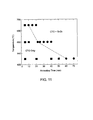
- FIG. 11 illustrates the effect of temperature and time on the composition of thermally treated cadmium tin oxide layers. As noted in FIG. 11 two distinct regions of cadmium tin oxide and tin oxide may be obtained by varying the temperature and time of thermal processing.
- the amorphous cadmium tin oxide layer is heated at the treatment temperature in a range from about 600°C to about 695°C. In another embodiment, the amorphous cadmium tin oxide layer is heated at the treatment temperature in a range from about 620°C to about 680°C. In a particular embodiment, the amorphous cadmium tin oxide layer is heated at the treatment temperature in a range from about 630°C to about 660°C.
- the amorphous cadmium tin oxide layer is heated at the treatment temperature for a time duration in a range from about 1 minute to about 70 minutes. In another embodiment, the amorphous cadmium tin oxide layer is heated at the treatment temperature for a time duration in a range from about 10 minutes to about 60 minutes. In a particular embodiment, the amorphous cadmium tin oxide layer is heated at the treatment temperature for a time duration in a range from about 20 minutes to about 40 minutes.
- the composition of the second region 340 may be further controlled by varying the pressure conditions employed during thermal processing.
- thermal processing is carried out under vacuum conditions, defmed here in as pressure conditions less than atmospheric pressure.
- thermal processing may be carried out in the presence of argon gas at a constant pressure.
- thermal processing may be carried out under dynamic pressure by continuous pumping.
- thermal processing is conducted in the presence of argon gas at a pressure less than about 500 Torr.
- thermal processing is conducted in the presence of argon gas at a pressure equal to or less than about 250 Torr.
- thermal processing is conducted in the presence of argon gas at a pressure equal to or less than about 50 Torr.
- thermal processing is conducted in the presence of argon gas at a pressure equal to or less than about 10 -3 Torr.
- the first region 320, the second region 340, and the transition region 360 are formed within the transparent layer 300 by sublimation of cadmium from the amorphous cadmium tin oxide layer.
- sublimation of cadmium from the cadmium tin oxide layer is non-stoichiometric resulting in a concentration gradient of cadmium within the layer.
- the concentration gradient is advantageously controlled by varying the thermal processing conditions (temperature, time and vacuum) to form the first region 320, the transition region 360, and the second region 340 within the transparent layer 300.
- the method further includes the steps of disposing a first semiconductor layer 400 on the transparent layer 300 after the step of thermal processing, disposing a second semiconductor layer 500 on the first semiconductor layer 400, and disposing a back contact layer 600 on the second semiconductor layer 500 to form a photovoltaic device 10.
- the first semiconductor layer 400 is disposed directly on the transparent layer 300 and an intermediate step of depositing an additional buffer layer is not required.
- an additional buffer layer 700 is disposed on the transparent layer 300 adjacent to the second region 340 after the thermal processing step. In such embodiments, the first 400 semiconductor layer is disposed on the buffer layer 700.
- One or more of the first semiconductor layer 400, second semiconductor layer 500, back contact layer 600, or the buffer layer (optional) 700 may be deposited by one or more of the following techniques: sputtering, electrodepositing, screen printing, spraying, physical vapor depositing, or closed space sublimation. One or more of these layers may be further heated or subsequently treated to manufacture the photovoltaic device 10.
- CTO cadmium tin oxide
- Thin films of cadmium tin oxide (CTO) were prepared on a 1.3 mm thick glass substrate by non-reactive magnetron DC sputtering from a pre-reacted cadmium stannate target having a 2:1 Cd:Sn ratio.
- the sputtering process was performed in an atmosphere containing oxygen and argon (wherein the concentration of oxygen was greater than 90%) at a pressure of about 16 mTorr.
- the thickness of the sputtered CTO film was in a range from 200 nm to 400nm.
- Annealing was carried out by placing the CTO films prepared above in contact with a CdS-coated glass substrate (referred to herein as CdS proximity annealing). The assembly was heated to a temperature of 630 °C for about 20 minutes in the presence of argon at a pressure of about 150 Torr.
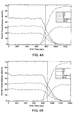
- FIG. 4A shows the XPS profile of as-deposited cadmium tin oxide film illustrating that the cadmium to tin atomic ratio is homogeneous across the thickness of the film.
- FIG. 4B shows the XPS profile of the CdS proximity-annealed cadmium tin oxide film illustrating that there was no change in atomic concentration of cadmium and tin and the corresponding atomic ratio after the annealing step. Further, no gradation in atomic concentration was observed for CTO films annealed using CdS film. As described above, a separate buffer or HRT layer may be deposited on the annealed CTO layer to obtain the desired configuration and performance properties of photovoltaic devices manufactured using these CTO films.
- CTO cadmium tin oxide
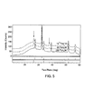
- FIG. 5 shows the X-ray diffraction patterns obtained from the three set of samples annealed at three different pressures indicate clear presence of tin oxide peaks (marked by arrows) for the samples sealed under vacuum at 10 -5 Torr and at 50 Torr.
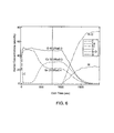
- FIG. 6 shows the XPS profile of cadmium tin oxide film annealed under vacuum at 10 -5 Torr.
- the CTO film showed three different concentration profiles: (a) a first region showing a constant atomic ratio of cadmium to tin for etch times in the range of about 600 seconds to about 1000 seconds; (b) a substantially cadmium-depleted region for etch times in the range of 0 second to about 300 seconds; and (c) a transition region for etch times in the range of 300 seconds to about 600 seconds in which the atomic concentration of cadmium and tin varies across the thickness of the transition region.
- the first region had the same atomic ratio of cadmium to tin as observed for the as-deposited amorphous cadmium tin oxide film ( FIG. 4A ).
- the XPS profile in FIG. 6 confirmed the presence of a substantially cadmium-free region having a thickness of about 50 nm after the annealing step.
- the substantially cadmium-free region may function as the buffer layer in some embodiments of the invention thus obviating the need for a separate step of depositing a buffer layer on the CTO layer.
- a first semiconductor layer of CdS may be deposited directly on the annealed CTO layer.
- the substantially cadmium-free region may provide a better interface between the annealed CTO layer and the additional buffer layer disposed on the CTO layer, enabling enhanced crystallization and performance of the buffer layer.
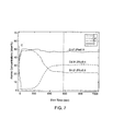
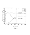
- FIG. 7 and FIG. 8 show the XPS profiles of cadmium tin oxide films annealed at a pressure of 50 Torr and 250 Torr, respectively. Similar to FIG. 6 , the XPS profiles in FIG. 7 and FIG.8 illustrate the formation of three different concentration profiles of cadmium and tin. A substantially cadmium-free region of about 50 nm was observed for sample annealed at 50 Torr as seen in FIG. 7 . FIG. 8 also illustrates severe depletion of cadmium in the first 50 nm of the film. However, the presence of cadmium at an atomic concentration less than about 5% is also observed throughout the surface of the film. This indicates that the atomic ratio and thickness of the tin-oxide rich region (second region) may be modified by varying the annealing pressure conditions.
- Example 3 Annealing of cadmium tin oxide without CdS film at different temperatures and for different time duration.
- CTO cadmium tin oxide
- FIG. 9 shows the XRD pattern for the CTO films annealed for different time durations. As illustrated in FIG. 9 , tin oxide peaks are observed more prominently as the annealing time duration increases from 10 minutes to 40 minutes.
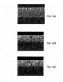
- FIG. 10A shows the scanning electron microscopy (SEM) micrograph for an un-annealed CTO film.
- Figs 10B and 10C show the scanning electron microscopy (SEM) micrographs for CTO films annealed for 25 minutes and 40 minutes, respectively. As illustrated in FIG. 10B after 25 minutes, a tin-oxide rich surface was observed.
- FIG. 10C illustrates that after 40 minutes of annealing cadmium is completely removed from the film.
- FIG. 10A shows the scanning electron microscopy (SEM) micrograph for an un-annealed CTO film.
- Figs 10B and 10C show the scanning electron microscopy (SEM) micrographs for CTO films annealed for 25 minutes and 40 minutes, respectively. As
- FIG. 11 shows an annealing time -temperature phase diagram for CTO films. As indicated in FIG. 11 , different combinations of annealing temperatures and times result in tin oxide-rich region (second region). Further, as described above, the atomic concentration and thickness of the tin oxide-rich region (second region) may be modified by varying one or both of annealing temperature or time duration of annealing.
- the word "comprises” and its grammatical variants logically also subtend and include phrases of varying and differing extent such as for example, but not limited thereto, “consisting essentially of” and “consisting of.” Where necessary, ranges have been supplied; those ranges are inclusive of all sub-ranges there between. It is to be expected that variations in these ranges will suggest themselves to a practitioner having ordinary skill in the art and where not already dedicated to the public, those variations should where possible be construed to be covered by the appended claims. It is also anticipated that advances in science and technology will make equivalents and substitutions possible that are not now contemplated by reason of the imprecision of language and these variations should also be construed where possible to be covered by the appended claims.
Landscapes
- Photovoltaic Devices (AREA)
- Electrodes Of Semiconductors (AREA)
Abstract
Description
- The invention relates to photovoltaic devices with enhanced cell performance and reduced cost of manufacturing. More particularly, the invention relates to transparent electrodes having graded cadmium tin oxide layer for use in photovoltaic devices.
- Thin film solar cells or photovoltaic devices typically include a plurality of semiconductor layers disposed on a transparent substrate, wherein one layer serves as a window layer and a second layer serves as an absorber layer. The window layer allows the penetration of solar radiation to the absorber layer, where the optical energy is converted to usable electrical energy. Cadmium telluride/cadmium sulfide (CdTe/CdS) heterojunction-based photovoltaic cells are one such example of thin films solar cells
- Typically, a thin layer of transparent conductive oxide (TCO) is deposited between the substrate and the window layer (for example, CdS) to function as a front contact current collector. However conventional TCOs, such as tin oxide, indium tin oxide, and zinc oxide, have high electrical resistivities at thickness necessary for good optical transmission. The use of cadmium tin oxide (CTO) as TCO provides better electrical, optical, and mechanical properties, as well as stability at elevated temperatures. However, CTO/CdS-based thin film solar cells still have challenges, for example, thick CdS films typically result in low device efficiencies whereas thin CdS films lead to reduced open circuit voltage (VOC).
- In some instances, to achieve high device efficiencies with thin CdS films, a thin layer of a buffer material, such as a tin oxide (SnO2) layer, is intercalated between the cadmium tin oxide (CTO) and the window (CdS) layers. The typical method used to manufacture the CTO layer includes depositing a layer of amorphous cadmium tin oxide on a substrate, followed by slow thermal annealing of the CTO layer, which is in contact with a CdS film, to achieve desired transparency and resistivity. However, CdS-based annealing of CTO is difficult to implement in a large-scale manufacturing environment. Further, the use of expensive CdS increases the cost of manufacturing. After crystallization of CTO is achieved, a separate buffer layer (for example, tin oxide) is deposited on the CTO layer, which may be further followed by a second annealing step to obtain good crystalline quality. The performance of the buffer layer usually depends in part on the crystallinity and morphology of that layer and is affected by the surface of the CTO on which it is deposited. A high quality buffer layer is desirable to obtain the desired performance in the solar cells manufactured therefrom.
- Thus, there is a need to provide improved electrodes and photovoltaic devices manufactured from CTO and buffer layers having desired electrical and optical properties. Further, there is a need to reduce the number of steps for depositing and annealing of CTO and buffer layers during manufacturing of photovoltaic devices, resulting in reduced costs and improved manufacturing capability.
- Embodiments of the present invention are provided to meet these and other needs. One embodiment is a transparent electrode. The transparent electrode includes a substrate and a transparent layer disposed on the substrate. The transparent layer includes (a) a first region including cadmium tin oxide; (b) a second region including tin and oxygen; and (c) a transition region including cadmium, tin, and oxygen interposed between the first region and the second region, wherein an atomic ratio of cadmium to tin in the transition region varies across a thickness of the transition region. The second region has an electrical resistivity greater than an electrical resistivity of the first region.
- One embodiment is a photovoltaic device. The photovoltaic device includes a substrate; a transparent layer disposed on the substrate; a first semiconductor layer disposed on the transparent layer; a second semiconductor layer disposed on the first semiconductor layer; and a back contact layer disposed on the second semiconductor layer. The transparent layer includes (a) a first region including cadmium tin oxide, (b) a second region including tin and oxygen, and (c) a transition region including cadmium, tin, and oxygen interposed between the first region and the second region, wherein an atomic ratio of cadmium to tin in the transition region varies across a thickness of the transition region. The second region has an electrical resistivity greater than an electrical resistivity of the first region.
- One embodiment is a photovoltaic module including a plurality of photovoltaic devices as described above.
- Another embodiment is a method. The method includes disposing a substantially amorphous cadmium tin oxide layer on a substrate and thermally processing the substantially amorphous cadmium tin oxide layer to form a transparent layer, wherein thermally processing includes heating the substantially amorphous cadmium tin oxide layer at a treatment temperature, under vacuum conditions, and for a time duration sufficient to allow formation of (a) a first region including cadmium tin oxide, (b) a second region including tin and oxygen, and (c) a transition region including cadmium, tin, and oxygen interposed between the first region and the second region, wherein an atomic ratio of cadmium to tin in the transition region varies across a thickness of the transition region. The second region has an electrical resistivity greater than an electrical resistivity of the first region.
- These and other features, aspects, and advantages of the present invention will become better understood when the following detailed description is read with reference to the accompanying drawings, wherein:
-
FIG. 1 is a schematic of a transparent electrode, according to one embodiment of the present invention. -
FIG. 2 is a schematic of a photovoltaic device, according to one embodiment of the present invention. -
FIG. 3 is a schematic of a photovoltaic device, according to one embodiment of the present invention. -
FIG. 4A shows the XPS profile of as-deposited amorphous cadmium tin oxide layer. -
FIG. 4B shows the XPS profile of crystalline cadmium tin oxide layer annealed in contact with CdS film. -
FIG. 5 shows the XRD patterns of a transparent layer, according to an exemplary embodiment of the invention. -
FIG. 6 shows the XPS profile of a transparent layer, according to an exemplary embodiment of the invention. -
FIG. 7 shows the XPS profile of a transparent layer, according to an exemplary embodiment of the invention. -
FIG. 8 shows the XPS profile of a transparent layer, according to an exemplary embodiment of the invention. -
FIG. 9 shows the XRD pattern of a transparent layer, according to an exemplary embodiment of the invention. -
FIG. 10A shows the micrograph of an un-annealed amorphous cadmium tin oxide layer. -
FIG. 10B shows the micrograph of a transparent layer, according to an exemplary embodiment of the invention. -
FIG. 10C the micrograph of a transparent layer, according to an exemplary embodiment of the invention. -
FIG. 11 shows the effect of time and temperature on the composition of the cadmium tin oxide layer, according to an exemplary embodiment of the invention. - As discussed in detail below, some of the embodiments of the invention provide transparent electrodes and photovoltaic devices having a graded cadmium tin oxide layer. The graded cadmium tin oxide layer may advantageously function as a transparent conductive oxide (TCO) layer and a buffer layer in some embodiments or alternatively facilitate disposing of a crystalline buffer layer in some other embodiments, enabling enhanced crystallization and performance of the buffer layer.
- Further, the graded cadmium tin oxide layer of the present invention may substantially eliminate the discontinuous interface between the TCO layer and the buffer layer characteristic of device structures that are fabricated by depositing first the TCO layer and then the buffer layer. Thus, the graded cadmium tin oxide layer may provide for improved adhesion between the TCO layer and the CdS layer and accordingly lower contact resistance and reduce optical losses as compared to a bilayer of buffer layer and TCO. In contrast, a bilayer of TCO layer and a buffer layer may have a higher propensity to accumulate impurities at the interface between the TCO layer and the buffer layer leading to increased defect formation. The graded layer may also relieve stresses at the interface between the TCO layer and CdS, and thus create a lower stress level at the CdS/CdTe interface, where defects contribute to lowering the Voc of these devices. The graded cadmium tin oxide layer may thus provide cost reduction during fabrication of the photovoltaic device and enhanced device performance by decreasing the optical absorption in the window layers, reducing the total optical losses, and optimizing the open-circuit voltage of the device.
- Approximating language, as used herein throughout the specification and claims, may be applied to modify any quantitative representation that could permissibly vary without resulting in a change in the basic function to which it is related. Accordingly, a value modified by a term or terms, such as "about", is not limited to the precise value specified. In some instances, the approximating language may correspond to the precision of an instrument for measuring the value.
- In the following specification and the claims, the singular forms "a", "an" and "the" include plural referents unless the context clearly dictates otherwise.
- As used herein, the terms "may" and "may be" indicate a possibility of an occurrence within a set of circumstances; a possession of a specified property, characteristic or function; and/or qualify another verb by expressing one or more of an ability, capability, or possibility associated with the qualified verb. Accordingly, usage of "may" and "may be" indicates that a modified term is apparently appropriate, capable, or suitable for an indicated capacity, function, or usage, while taking into account that in some circumstances the modified term may sometimes not be appropriate, capable, or suitable. For example, in some circumstances, an event or capacity can be expected, while in other circumstances the event or capacity cannot occur ― this distinction is captured by the terms "may" and "may be".
- The terms "transparent region", "transparent layer" and "transparent electrode" as used herein, refer to a region, a layer, or an article that allows an average transmission of at least 80% of incident electromagnetic radiation having a wavelength in a range from about 300 nm to about 850 nm. As used herein, the term "disposed on" refers to layers disposed directly in contact with each other or indirectly by having intervening layers therebetween.
- As discussed in detail below, some embodiments of the invention are directed to an improved transparent electrode. A
transparent electrode 100 according to one embodiment of the invention is illustrated inFIG. 1 . Thetransparent electrode 100 includes asubstrate 200 and atransparent layer 300 disposed on thesubstrate 200. Thetransparent layer 300 further includes afirst region 320, asecond region 340, and atransition region 360 interposed between thefirst region 320 and thesecond region 340. Thefirst region 320 includes cadmium tin oxide, thesecond region 340 includes tin and oxygen, and thetransition region 360 includes cadmium, tin, and oxygen, wherein an atomic ratio of cadmium to tin in thetransition region 360 varies across a thickness of thetransition region 360. Thesecond region 340 has an electrical resistivity that is greater than that an electrical resistivity of thefirst region 320. - The
substrate 200 further includes afirst surface 201 and asecond surface 202, wherein the solar radiation is incident on thefirst surface 201 and thetransparent layer 300 is disposed adjacent to thesecond surface 202. In one embodiment, thesubstrate 200 is transparent over the range of wavelengths for which transmission through thesubstrate 200 is desired. In one embodiment, thesubstrate 200 may be transparent to visible light having a wavelength in a range from about 300 nm to about 850 nm. In another embodiment, thesubstrate 200 further includes a material capable of withstanding heat treatment temperatures greater than about 550 °C. In yet another embodiment, the thermal expansion coefficient of thesubstrate 200 is close to the thermal expansion coefficient of thetransparent layer 300 to prevent cracking or buckling of thetransparent layer 300 during heat treatment. Suitable examples of materials forsubstrate 200 include, but are not limited to, silica and glass. In a particular embodiment, thesubstrate 200 includes glass. Suitable examples of glass include, but are not limited to, soda-glass and borosilicate glass. - As described above, the
transparent layer 300 includes afirst region 320 and asecond region 340, wherein thesecond region 340 is more electrically resistive than thefirst region 320. In some embodiments, thetransparent layer 300 includes a graded cadmium tin oxide (CTO) layer wherein the concentration of cadmium and tin in the layer varies across the thickness of the layer. In a particular embodiment, thetransparent layer 300 includes a graded cadmium tin oxide (CTO) layer wherein the concentration of cadmium decreases from a first surface of thetransparent layer 301 to asecond surface 302 of the transparent layer, as illustrated inFIG. 1 . In some embodiments, thefirst region 320 functions as a transparent conductive oxide (TCO) layer and thesecond region 340 functions as buffer layer. Thus, in some embodiments, the composition of thetransparent layer 300 is advantageously engineered to vary across the thickness of the layer such that thetransparent layer 300 functions both as a TCO layer and a buffer layer. - The
first region 320 in thetransparent layer 300 includes cadmium tin oxide. As used herein, the term "cadmium tin oxide" includes a composition of cadmium, tin, and oxygen. In some embodiments, cadmium tin oxide includes a stoichiometric oxide composition of cadmium and tin, wherein, for example, the atomic ratio of cadmium to tin is about 2:1. In some other embodiments, cadmium tin oxide includes a non-stoichiometric oxide composition of cadmium and tin, wherein, for example, the atomic ratio of cadmium to tin is in a range less than about 2:1 or greater than about 2:1. As used herein, the terms "cadmium tin oxide" and "CTO" may be used interchangeably. In some embodiments, cadmium tin oxide may further include dopants, such as, for example, copper, zinc, calcium, yttrium, zirconium, hafnium, vanadium, tin, ruthenium, magnesium, indium, zinc, palladium, rhodium, titanium, or combinations thereof. In certain embodiments, cadmium tin oxide may function as a transparent conductive oxide (TCO). Cadmium tin oxide as a TCO has numerous advantages including superior electrical, optical, surface, and mechanical properties and increased stability at elevated temperatures when compared to tin oxide, indium oxide, indium tin oxide, and other transparent conductive oxides. - The electrical properties of the
first region 320 may depend in part on the composition of cadmium tin oxide characterized in some embodiments by the atomic concentration of cadmium and tin, or alternatively in some other embodiments by the atomic ratio of cadmium to tin in cadmium tin oxide. Accordingly, in some embodiments the atomic ratio of cadmium to tin in thefirst region 320 may be advantageously engineered to provide the desired electrical properties. Atomic ratio of cadmium to tin, as used herein, refers to the ratio of atomic concentration of cadmium to tin in cadmium tin oxide. Atomic concentrations of cadmium and tin and the corresponding atomic ratio are commonly measured using, for instance, x-ray photon spectroscopy (XPS). - In one embodiment, the atomic ratio of cadmium to tin in the
first region 320 is in a range from about 1.2:1 to about 3:1. In another embodiment, the atomic ratio of cadmium to tin in thefirst region 320 is in a range from about 1.4:1 to about 2.5:1. In yet another embodiment, the atomic ratio of cadmium to tin in thefirst region 320 is in a range from about 1.7:1 to about 2.15:1. In one particular embodiment, the atomic ratio of cadmium to tin in thefirst region 320 is in a range from about 1.5:1 to about 2:1. - In one embodiment, atomic concentration of cadmium is in a range from about 20% to about 40% of the total atomic content of cadmium tin oxide. In another embodiment, atomic concentration of cadmium is in a range from about 25% to about 35% of the total atomic content of cadmium tin oxide. In a particular embodiment, atomic concentration of cadmium is in a range from about 28% to about 32% of the total atomic content of cadmium tin oxide. In one embodiment, atomic concentration of tin is in a range from about 10% to about 30% of the total atomic content of cadmium tin oxide. In another embodiment, atomic concentration of tin is in a range from about 15% to about 28% of the total atomic content of cadmium tin oxide. In a particular embodiment, atomic concentration of tin is in a range from about 18% to about 24% of the total atomic content of cadmium tin oxide. In one embodiment, atomic concentration of oxygen is in a range from about 30% to about 70% of the total atomic content of cadmium tin oxide. In another embodiment, atomic concentration of oxygen is in a range from about 40% to about 60% of the total atomic content of cadmium tin oxide. In a particular embodiment, atomic concentration of oxygen is in a range from about 44% to about 50% of the total atomic content of cadmium tin oxide.
- In one embodiment, the atomic ratio of cadmium to tin in the
first region 320 is substantially constant across a thickness of thefirst region 320. The term "substantially constant" as used herein means that the variation in the atomic ratio of cadmium to tin is less than about 10% across the thickness of thefirst region 320. The electrical and optical properties of thefirst region 320 may also depend in part on the thickness of the cadmium tin oxide layer. In one embodiment, thefirst region 320 has a thickness in a range from about 100 nm to about 500 nm. In another embodiment, thefirst region 320 has a thickness in a range from about 150 nm to about 450 nm. In a particular embodiment, thefirst region 320 has a thickness in a range from about 100 nm to about 400 nm. In some embodiments, the higher conductivity of thefirst region 320 may complement the optical transmission. Higher conductivity or lower resistivity of thefirst region 320 may allow for a thinnerfirst region 320, which further increases the optical transmission. - As discussed in detail below, the
first region 320 is formed by disposing a substantially amorphous cadmium tin oxide layer on the substrate and thermally processing the amorphous cadmium tin oxide layer to form thefirst region 320 within thetransparent layer 300. "Substantially amorphous" as used herein refers to a cadmium tin oxide layer that does not have a crystalline pattern as observed by X-ray diffraction (XRD). In some embodiments, thefirst region 320 includes a uniform single-phase polycrystalline cadmium tin oxide, formed for example, by annealing the amorphous cadmium tin oxide layer. In some embodiments, the crystalline cadmium tin oxide has an inverse spinel crystal structure. The uniform single-phase crystalline cadmium tin oxide that forms thefirst region 320 is referred to herein as "cadmium tin oxide" as distinguished from a "substantially amorphous cadmium tin oxide" that is disposed on thesubstrate 200 and thermally treated to form thetransparent layer 300. - The
transparent layer 300 further includes asecond region 340 including tin and oxygen that is formed by thermal processing of the amorphous cadmium tin oxide layer. Thesecond region 340 may function as a buffer layer in some embodiments or may assist the nucleation of a separately deposited crystalline buffer (for example, tin oxide) layer on the CTO layer resulting in a higher quality buffer layer. In some embodiments, thesecond region 340 is formed by non-stoichiometric sublimation of cadmium from cadmium tin oxide at annealing conditions employed during thermal processing. Without being bound by theory, it is believed that the vapor pressure of cadmium above the amorphous cadmium tin oxide layer is higher than that of tin, resulting in cadmium depletion at the surface during thermal processing. In some embodiments, controlled depletion of cadmium from the surface results in formation of thesecond region 340 having controlled thickness, morphology, and composition - As described above with reference to the
first region 320, the electrical properties of thesecond region 340 may also depend in part on the composition of thesecond region 340 or the concentration of cadmium to tin in thesecond region 340. In some embodiments, thesecond region 340 includes tin oxide. In some embodiments thesecond region 340 further includes cadmium. In one embodiment, the atomic concentration of cadmium in thesecond region 340 is less than about 10%. In another embodiment, the atomic concentration of cadmium in thesecond region 340 is less than about 5%. In a particular embodiment, the atomic concentration of cadmium in thesecond region 340 is less than about 0.5%. - In some other embodiments, the
second region 340 is substantially free of cadmium. "Substantially free of cadmium" as used herein means that the atomic concentration of cadmium in thesecond region 340 is less than about 0.01%. In one embodiment, the atomic concentration of cadmium in thesecond region 340 is less than about 0.001%. In one embodiment, the atomic concentration of cadmium in thesecond region 340 is about 0%. - In some embodiments, the atomic ratio of cadmium to tin in the second 340 region is substantially constant across a thickness of the
second region 340. As noted earlier, the term "substantially constant" as used herein means that the variation in the atomic ratio of cadmium to tin is less than about 10% across the thickness of thesecond region 340. In some embodiments, the thickness of thesecond region 340 is controlled by varying one or more of treatment temperature, time duration, and vacuum conditions employed during the thermal annealing process. In one embodiment, thickness of thesecond region 340 is engineered to be in a range from about 10 nm to about 300 nm. In another embodiment, thesecond region 340 has a thickness in a range from about 50 nm to about 250 nm. In a particular embodiment, thesecond region 340 has a thickness in a range from about 20 nm to about 200 nm. - The
transparent layer 300 further includes atransition region 360 interposed between thefirst region 320 and thesecond region 340. Thetransition region 360 includes cadmium, tin and oxygen. As mentioned above, the atomic ratio of cadmium to tin in thetransition region 360 varies across the thickness of thetransition region 360. In one particular embodiment, the atomic ratio of cadmium to tin in thetransition region 360 decreases from thefirst region 320 to thesecond region 340. - In some embodiments, the
transition region 360 includes a continuous gradient of atomic concentration of cadmium and tin. The continuous gradient of atomic concentrations of cadmium and tin in thetransition region 360 allows for continuous transition of composition between the first region 320 (functioning as a transparent conductive oxide (TCO) layer) and the second region 340 (functioning as a buffer layer). Thus, the graded cadmium tin oxide (CTO) layer of the present invention substantially eliminates the discontinuous interface between the TCO layer and the buffer layer characteristic of device structures that are fabricated by depositing first the TCO layer and then the buffer layer. The presence of discontinuous interfaces between functional layers in thin film solar cells may result in both optical and electrical losses. - In some embodiments, the thickness of the
transition region 360 is controlled by varying one or more of treatment temperature, time duration, and vacuum conditions employed during the thermal annealing process. In one embodiment, the thickness of thetransition region 360 is engineered to be in a range from about 10 nm to about 200 nm. In another embodiment, thetransition region 360 has a thickness in a range from about 20 nm to about 150 nm. In a particular embodiment, thetransition region 360 has a thickness in a range from about 40 nm to about 100 nm. - The
first region 320 and thesecond region 340 may be further characterized by their electrical and optical properties. In some embodiments, thesecond region 340 has an electrical resistivity that is greater than the electrical resistivity of thefirst region 320 by a factor of 1000. In some other embodiments, thesecond region 340 has an electrical resistivity that is greater than the electrical resistivity of thefirst region 320 by a factor of 100. In certain embodiments, thesecond region 340 has an electrical resistivity that is greater than the electrical resistivity of thefirst region 320 by a factor of 50. - In some embodiments, the
first region 320 has an average electrical resistivity (p) that is less than about 2.5 x10⁻⁴ Ohms-cm. In some other embodiments, thefirst region 320 has an average electrical resistivity (p) that is less than about 2x10⁻⁴ Ohms-cm. In some embodiments, thesecond region 340 has an average electrical resistivity (p) that is greater about 10-3 Ohms-cm. In some embodiments, thesecond region 340 has an average electrical resistivity (p) that is greater about 10-2 Ohms-cm. Thefirst region 320 and thesecond region 340 further have an average optical transmission greater than about 80%. In some embodiments, thetransparent electrode 100 has an average optical transmission greater than about 80%. In some other embodiments, thetransparent electrode 100 has an average optical transmission greater than about 95%. - As discussed in detail below, some embodiments of the invention are further directed to improved photovoltaic device designs. A photovoltaic device according to one embodiment of the invention is illustrated in
FIG. 2 . Thephotovoltaic device 10 includes asubstrate 200, atransparent layer 300 disposed on thesubstrate 200, afirst semiconductor layer 400 disposed on thetransparent layer 300, asecond semiconductor layer 500 disposed on thefirst semiconductor layer 400, and aback contact layer 600 disposed on thesecond semiconductor layer 500. Thetransparent layer 300 includes afirst region 320, asecond region 340, and atransition region 360 interposed between thefirst region 320 and thesecond region 340. - In some embodiments, the first
type semiconductor layer 400 and thesecond semiconductor layer 500 may be doped with a p-type dopant or n-type dopant to form a heterojunction. As used in this context, a heterojunction is a semiconductor junction, which is composed of layers of dissimilar semiconductor material. These materials usually have non-equal band gaps. As an example, a heterojunction can be formed by contact between a layer or region of one conductivity type with a layer or region of opposite conductivity, e.g., a "p-n" junction. In addition to solar cells, other devices that utilize the heterojunction include thin film transistors and bipolar transistors. - In some embodiments, the
second semiconductor layer 500 includes an absorber layer. The absorber layer is a part of a photovoltaic device where the conversion of electromagnetic energy of incident light (for instance, sunlight) to electron-hole pairs (that is, to electrical current) occurs. A photo-active material is typically used for forming the absorber layer. Suitable photo-active materials include cadmium telluride (CdTe), cadmium zinc telluride (CdZnTe), cadmium magnesium telluride (CdMgTe), cadmium manganese telluride (CdMnTe), cadmium sulfur telluride (CdSTe), zinc telluride (ZnTe), CIS (copper, indium, sulphur), CIGS (copper, indium, gallium, selenium), and combinations thereof. The above-mentioned photo-active semiconductor materials may be used alone or in combination. Further, these materials may be present in more than one layer, each layer having different type of photo-active material or having combinations of the materials in separate layers. In one particular embodiment, thesecond semiconductor layer 500 or the absorber layer includes cadmium telluride (CdTe) as the photo-active material. CdTe is an efficient photo-active material that is used in thin-film photovoltaic devices. CdTe is relatively easy to deposit and therefore is considered suitable for large-scale production. In one embodiment, the second semiconductor layer has a thickness in a range from about 1500 nm to about 4000 nm. - The
first semiconductor layer 400 is disposed adjacent to thesecond region 340 of thetransparent layer 300. In a particular embodiment, thefirst semiconductor layer 400 includes cadmium sulfide (CdS) and may be referred to as the "window layer". The window layer is typically transparent to a substantial portion of solar radiation entering from thetransparent substrate 200. However, the CdS layer may not be completely transparent to solar radiation, especially in the range of shorter wavelength, that is, less than 500 nm. Accordingly, a thin CdS layer may be desirable because the thinner the CdS layer, the greater is the portion of shorter wavelength solar radiation that may be transferred into the CdTe layer to be absorbed and converted into electrical energy. However, thinner CdS layers may have more likelihood of pinholes or other defects, resulting in lower open circuit voltage (Voc) of the photovoltaic device. According to some embodiments of the invention, the graded cadmium tin oxide (CTO) layer may advantageously allow for thinner CdS layer to be used without compromising on the photovoltaic device performance. In such embodiments, thesecond region 340 may function as a buffer layer or insulating layer between the CdTe and the first region 320 (functioning as TCO) if the CdS has pinholes. Further, thesecond region 340 may also relieve stress at the interface between the first region 320 (functioning as TCO) and CdS, and thus create a lower stress level at the CdS/CdTe interface, where defects contribute to lowering the Voc of these devices. Accordingly, thesecond region 340 within thetransparent layer 300 may obviate the need to dispose an additional buffer layer between the CTO layer and the first semiconductor layer 400 (for example, CdS) in certain embodiments. In one embodiment, thefirst semiconductor layer 400 has a thickness in a range from about 30 nm to about 150 nm. - In some embodiments, the photovoltaic device further includes a buffer layer disposed between the transparent layer and the first semiconductor layer. In such embodiments, the buffer layer is disposed adjacent to the
second region 340 such that thesecond region 340 facilitates disposing of higher quality buffer layer on the cadmium tin oxide (CTO) layer and further reduces the effect of discontinuous interface between the cadmium tin oxide (CTO) layer and the buffer layer. As illustrated inFIG. 3 , thephotovoltaic device 10 includes asubstrate 200, atransparent layer 300 disposed on thesubstrate 200, afirst semiconductor layer 400 disposed on thetransparent layer 300, asecond semiconductor layer 500 disposed on thefirst semiconductor layer 400, and aback contact layer 600 disposed on thesecond semiconductor layer 500. Thetransparent layer 300 includes afirst region 320, asecond region 340, and atransition region 360 interposed between thefirst region 320 and thesecond region 340. Thephotovoltaic device 10 further includes abuffer layer 700 disposed adjacent to thesecond region 340 and interposed between thetransparent layer 300 and thefirst semiconductor layer 400. - In one embodiment, the
buffer layer 700 includes an oxide selected from the group consisting of tin oxide, indium oxide, zinc oxide, zinc stannate, and combinations thereof. In a particular embodiment, thebuffer layer 700 includes tin oxide or ternary mixed oxide thereof. - A
back contact layer 600 is further disposed adjacent to thesecond semiconductor layer 500 and is in ohmic contact therewith. Backcontact layer 600 may include a metal, semiconductor, or combination thereof. In some embodiments, aback contact layer 600 may include gold, platinum, molybdenum, or nickel, or zinc telluride. In some embodiments, one or more additional layers may be interposed between thesecond semiconductor layer 500 and theback contact layer 600, such as, for example, a p+-type semiconductor layer. In some embodiments, thesecond semiconductor layer 500 may include p-type cadmium telluride (CdTe) that may be further treated or doped to improve the back contact resistance, such as for example, by cadmium chloride treatment or by forming a zinc telluride or copper telluride layer on the backside. In one embodiment, the back contact resistance may be improved by increasing the p type carriers in the CdTe material to form a p+ type layer on the backside of the CdTe material that is in contact with the back contact layer. - In one embodiment, a photovoltaic module is provided. The photovoltaic module may have an array of a number of photovoltaic devices described above electrically connected in series or in parallel. Substantially all photovoltaic devices include the
transparent electrode 100 as discussed in above embodiments. - In one embodiment, a method of making the
transparent electrode 100 is provided. The method includes disposing a substantially amorphous cadmium tin oxide layer on asubstrate 200; and thermally processing the amorphous cadmium tin oxide layer to form atransparent layer 300. Thermal processing of the amorphous cadmium tin oxide layer includes heating the substantially amorphous cadmium tin oxide layer at a treatment temperature, under vacuum conditions, and for time duration sufficient to allow formation of thefirst region 320, thesecond region 340, and thetransition region 360. - In one embodiment, the substantially amorphous cadmium tin oxide layer is deposited on the
substrate 200 by any suitable technique, such as sputtering, chemical vapor depositing, spin coating, spray coating, or dip coating. In one embodiment, the substantially amorphous cadmium tin oxide layer may be formed by dipping asubstrate 200 into a solution of a reaction product containing cadmium and tin derived from a cadmium compound and a tin compound. - In a particular embodiment, the substantially amorphous cadmium tin oxide layer is deposited on the
substrate 200 by sputtering. In one embodiment, the substantially amorphous cadmium tin oxide layer may be deposited on the substrate by 200 radio frequency (RF) sputtering or direct current (DC) magnetron sputtering. In one embodiment, the substantially amorphous cadmium tin oxide layer may be deposited by reactive sputtering in the presence of oxygen. - In some embodiments, the substantially amorphous cadmium tin oxide layer is disposed on the
substrate 200 using a ceramic cadmium tin oxide target. In some other embodiments, a substantially amorphous cadmium tin oxide layer is disposed on thesubstrate 200 by co-sputtering using cadmium oxide and tin oxide targets or by sputtering from a single target including a blend of cadmium oxide and tin oxide. In some other embodiments, a substantially amorphous cadmium tin oxide layer is disposed on thesubstrate 200 by reactive sputtering using a single metallic target, wherein the metal target includes a mixture of cadmium and tin metals or by reactive co-sputtering using two different metal targets, that is, a cadmium target and a tin target. The sputtering target(s) may be manufactured, formed, or shaped by any process and in any shape, composition, or configuration suitable for use with any appropriate sputtering tool, machine, apparatus, or system. - When depositing a cadmium tin oxide layer on the
substrate 200 by sputtering, the atomic concentration of cadmium and tin in the deposited layer may be directly proportional to the atomic concentration of cadmium and tin in the sputtering target(s). In one embodiment, the atomic ratio of cadmium to tin in the sputtering target(s) is in a range from about 1.2:1 to about 3:1. In another embodiment, the atomic ratio of cadmium to tin in the sputtering target(s) is in a range from about 1.7:1 to about 2.5:1. In one particular embodiment, the atomic ratio of cadmium to tin in sputtering target(s) is in a range from about 1.5:1 to about 2:1. In some embodiments, the atomic concentration of cadmium and tin in thefirst region 320 of thetransparent layer 300 is directly proportional to the atomic concentration of cadmium and tin in the target(s). - The as-deposited cadmium tin oxide layer is substantially amorphous. The amorphous cadmium tin oxide layer is further thermally processed by heating the amorphous cadmium tin oxide layer. In some embodiments, thermally processing the amorphous cadmium tin oxide layer forms a
first region 320 that includes cadmium tin oxide having a substantially single-phase spinel crystal structure. As noted herein earlier, the thermal processing step is carried out in the absence of a CdS film or any additional external source of cadmium that is conventionally used for annealing cadmium tin oxide. Accordingly, the thermal processing step of the present invention eliminates the additional step of preparing a CdS film on asubstrate 200 that is later used for annealing of cadmium tin oxide. Further, it also reduces the amount of CdS used in the fabrication of a photovoltaic device, and is economically advantageous as CdS is an expensive material. - Thermal processing of the cadmium tin oxide layer is carried out by heating the amorphous cadmium tin oxide layer to further allow for formation of a
second region 340 and atransition region 360. As described above, thesecond region 340 may function as a buffer layer. Accordingly, in some embodiments, the thermal processing step eliminates the need for a separate step for depositing the additional buffer layer thus reducing the cost of fabrication. In some other embodiments, the thermal processing step may provide for an improved interface between the first region 320 (functioning as TCO) and the additional buffer layer by controlling the thickness, morphology, and composition of thesecond region 340. - The composition, thickness, and morphology of the
first region 320, thesecond region 340, and thetransition region 360 are advantageously controlled by varying one or more of treatment temperature, time duration of heat treatment, and vacuum conditions employed during heat treatment.FIG. 11 illustrates the effect of temperature and time on the composition of thermally treated cadmium tin oxide layers. As noted inFIG. 11 two distinct regions of cadmium tin oxide and tin oxide may be obtained by varying the temperature and time of thermal processing. - In one embodiment, the amorphous cadmium tin oxide layer is heated at the treatment temperature in a range from about 600°C to about 695°C. In another embodiment, the amorphous cadmium tin oxide layer is heated at the treatment temperature in a range from about 620°C to about 680°C. In a particular embodiment, the amorphous cadmium tin oxide layer is heated at the treatment temperature in a range from about 630°C to about 660°C.
- In one embodiment, the amorphous cadmium tin oxide layer is heated at the treatment temperature for a time duration in a range from about 1 minute to about 70 minutes. In another embodiment, the amorphous cadmium tin oxide layer is heated at the treatment temperature for a time duration in a range from about 10 minutes to about 60 minutes. In a particular embodiment, the amorphous cadmium tin oxide layer is heated at the treatment temperature for a time duration in a range from about 20 minutes to about 40 minutes.
- The composition of the
second region 340 may be further controlled by varying the pressure conditions employed during thermal processing. In one embodiment, thermal processing is carried out under vacuum conditions, defmed here in as pressure conditions less than atmospheric pressure. In some embodiments, thermal processing may be carried out in the presence of argon gas at a constant pressure. In some other embodiments, thermal processing may be carried out under dynamic pressure by continuous pumping. In one embodiment, thermal processing is conducted in the presence of argon gas at a pressure less than about 500 Torr. In another embodiment, thermal processing is conducted in the presence of argon gas at a pressure equal to or less than about 250 Torr. In yet another embodiment, thermal processing is conducted in the presence of argon gas at a pressure equal to or less than about 50 Torr. In a particular embodiment, thermal processing is conducted in the presence of argon gas at a pressure equal to or less than about 10-3 Torr. - In some embodiments, the
first region 320, thesecond region 340, and thetransition region 360 are formed within thetransparent layer 300 by sublimation of cadmium from the amorphous cadmium tin oxide layer. In some embodiments, sublimation of cadmium from the cadmium tin oxide layer is non-stoichiometric resulting in a concentration gradient of cadmium within the layer. The concentration gradient is advantageously controlled by varying the thermal processing conditions (temperature, time and vacuum) to form thefirst region 320, thetransition region 360, and thesecond region 340 within thetransparent layer 300. - In one embodiment, the method further includes the steps of disposing a
first semiconductor layer 400 on thetransparent layer 300 after the step of thermal processing, disposing asecond semiconductor layer 500 on thefirst semiconductor layer 400, and disposing aback contact layer 600 on thesecond semiconductor layer 500 to form aphotovoltaic device 10. In some embodiments, thefirst semiconductor layer 400 is disposed directly on thetransparent layer 300 and an intermediate step of depositing an additional buffer layer is not required. In some other embodiments, anadditional buffer layer 700 is disposed on thetransparent layer 300 adjacent to thesecond region 340 after the thermal processing step. In such embodiments, the first 400 semiconductor layer is disposed on thebuffer layer 700. - One or more of the
first semiconductor layer 400,second semiconductor layer 500,back contact layer 600, or the buffer layer (optional) 700 may be deposited by one or more of the following techniques: sputtering, electrodepositing, screen printing, spraying, physical vapor depositing, or closed space sublimation. One or more of these layers may be further heated or subsequently treated to manufacture thephotovoltaic device 10. - The following examples are presented to further illustrate certain embodiments of the present invention. These examples should not be read to limit the invention in any way.
- Thin films of cadmium tin oxide (CTO) were prepared on a 1.3 mm thick glass substrate by non-reactive magnetron DC sputtering from a pre-reacted cadmium stannate target having a 2:1 Cd:Sn ratio. The sputtering process was performed in an atmosphere containing oxygen and argon (wherein the concentration of oxygen was greater than 90%) at a pressure of about 16 mTorr. The thickness of the sputtered CTO film was in a range from 200 nm to 400nm. Annealing was carried out by placing the CTO films prepared above in contact with a CdS-coated glass substrate (referred to herein as CdS proximity annealing). The assembly was heated to a temperature of 630 °C for about 20 minutes in the presence of argon at a pressure of about 150 Torr.
-
FIG. 4A shows the XPS profile of as-deposited cadmium tin oxide film illustrating that the cadmium to tin atomic ratio is homogeneous across the thickness of the film.FIG. 4B shows the XPS profile of the CdS proximity-annealed cadmium tin oxide film illustrating that there was no change in atomic concentration of cadmium and tin and the corresponding atomic ratio after the annealing step. Further, no gradation in atomic concentration was observed for CTO films annealed using CdS film. As described above, a separate buffer or HRT layer may be deposited on the annealed CTO layer to obtain the desired configuration and performance properties of photovoltaic devices manufactured using these CTO films. - Thin films of cadmium tin oxide (CTO) were prepared on a glass substrate using the method as described in Example 1. Three CTO samples (0.5 inches x 1 inch) were cut and sealed in 0.75 inches diameter quartz ampoules. The ampoules were filled with argon gas at three different vacuum levels: 10-5 Torr, 50 Torr, and 250 Torr, respectively. These samples were then annealed at 630 °C for about 20 minutes.
-
FIG. 5 shows the X-ray diffraction patterns obtained from the three set of samples annealed at three different pressures indicate clear presence of tin oxide peaks (marked by arrows) for the samples sealed under vacuum at 10-5 Torr and at 50 Torr.FIG. 6 shows the XPS profile of cadmium tin oxide film annealed under vacuum at 10-5 Torr.FIG. 6 illustrates that after annealing, the CTO film showed three different concentration profiles: (a) a first region showing a constant atomic ratio of cadmium to tin for etch times in the range of about 600 seconds to about 1000 seconds; (b) a substantially cadmium-depleted region for etch times in the range of 0 second to about 300 seconds; and (c) a transition region for etch times in the range of 300 seconds to about 600 seconds in which the atomic concentration of cadmium and tin varies across the thickness of the transition region. As illustrated inFIG. 6 , the first region had the same atomic ratio of cadmium to tin as observed for the as-deposited amorphous cadmium tin oxide film (FIG. 4A ). Further, the XPS profile inFIG. 6 confirmed the presence of a substantially cadmium-free region having a thickness of about 50 nm after the annealing step. As described above, the substantially cadmium-free region may function as the buffer layer in some embodiments of the invention thus obviating the need for a separate step of depositing a buffer layer on the CTO layer. In such instances a first semiconductor layer of CdS may be deposited directly on the annealed CTO layer. In some other embodiments, the substantially cadmium-free region may provide a better interface between the annealed CTO layer and the additional buffer layer disposed on the CTO layer, enabling enhanced crystallization and performance of the buffer layer. -
FIG. 7 andFIG. 8 show the XPS profiles of cadmium tin oxide films annealed at a pressure of 50 Torr and 250 Torr, respectively. Similar toFIG. 6 , the XPS profiles inFIG. 7 andFIG.8 illustrate the formation of three different concentration profiles of cadmium and tin. A substantially cadmium-free region of about 50 nm was observed for sample annealed at 50 Torr as seen inFIG. 7 .FIG. 8 also illustrates severe depletion of cadmium in the first 50 nm of the film. However, the presence of cadmium at an atomic concentration less than about 5% is also observed throughout the surface of the film. This indicates that the atomic ratio and thickness of the tin-oxide rich region (second region) may be modified by varying the annealing pressure conditions. - Thin films of cadmium tin oxide (CTO) were prepared on a glass substrate using the method as described in Example 1. The films were annealed at 660 °C under continuous pumping (vacuum) at a pressure below 10-3 Torr for time duration in a range of 10 minutes to 40 minutes.
-
FIG. 9 shows the XRD pattern for the CTO films annealed for different time durations. As illustrated inFIG. 9 , tin oxide peaks are observed more prominently as the annealing time duration increases from 10 minutes to 40 minutes.FIG. 10A shows the scanning electron microscopy (SEM) micrograph for an un-annealed CTO film.Figs 10B and 10C show the scanning electron microscopy (SEM) micrographs for CTO films annealed for 25 minutes and 40 minutes, respectively. As illustrated inFIG. 10B after 25 minutes, a tin-oxide rich surface was observed.FIG. 10C illustrates that after 40 minutes of annealing cadmium is completely removed from the film.FIG. 11 shows an annealing time -temperature phase diagram for CTO films. As indicated inFIG. 11 , different combinations of annealing temperatures and times result in tin oxide-rich region (second region). Further, as described above, the atomic concentration and thickness of the tin oxide-rich region (second region) may be modified by varying one or both of annealing temperature or time duration of annealing. - The foregoing examples are merely illustrative, serving to exemplify only some of the features of the invention. The appended claims are intended to claim the invention as broadly as it has been conceived and the examples herein presented are illustrative of selected embodiments from a manifold of all possible embodiments. Accordingly, it is the Applicants' intention that the appended claims are not to be limited by the choice of examples utilized to illustrate features of the present invention. As used in the claims, the word "comprises" and its grammatical variants logically also subtend and include phrases of varying and differing extent such as for example, but not limited thereto, "consisting essentially of" and "consisting of." Where necessary, ranges have been supplied; those ranges are inclusive of all sub-ranges there between. It is to be expected that variations in these ranges will suggest themselves to a practitioner having ordinary skill in the art and where not already dedicated to the public, those variations should where possible be construed to be covered by the appended claims. It is also anticipated that advances in science and technology will make equivalents and substitutions possible that are not now contemplated by reason of the imprecision of language and these variations should also be construed where possible to be covered by the appended claims.
- Various aspects and embodiments of the present invention are defined by the following numbered clauses:
- 1. A transparent electrode, comprising:
- a substrate; and
- a transparent layer disposed on the substrate, wherein the transparent layer comprises:
- (a) a first region comprising cadmium tin oxide,
- (b) a second region comprising tin and oxygen, and
- (c) a transition region comprising cadmium, tin, and oxygen interposed between the first region and the second region, wherein an atomic ratio of cadmium to tin in the transition region varies across a thickness of the transition region,
- wherein the second region has an electrical resistivity greater than an electrical resistivity of the first region.
- 2. The transparent electrode of
clause 1, wherein an atomic ratio of cadmium to tin in the first region is in a range from about 1.2:1 to about 3:1. - 3. The transparent electrode of
clause 1, wherein an atomic ratio of cadmium to tin in the first region is in a range from about 1.5: 1 to about 2:1. - 4. The transparent electrode of
clause 1, wherein an atomic ratio of cadmium to tin in the first region is substantially constant across a thickness of the first region. - 5. The transparent electrode of
clause 1, wherein the first region has a thickness in a range from about 100 nm to about 400 nm. - 6. The transparent electrode of
clause 1, wherein the cadmium tin oxide has a substantially single-phase spinel crystal structure. - 7. The transparent electrode of
clause 1, wherein the second region has a thickness in a range from about 20 nm to about 200 nm. - 8. The transparent electrode of
clause 1, wherein the second region further comprises cadmium and an atomic concentration of cadmium is less than about 5%. - 9. The transparent electrode of
clause 1, wherein the second region further comprises cadmium and an atomic concentration of cadmium is less than about 0.5%. - 10. The transparent electrode of
clause 1, wherein the second region is substantially free of cadmium. - 11. The transparent electrode of
clause 1, wherein the transition region has a thickness in a range from about 40 nm to about 100 nm. - 12. The transparent electrode of
clause 1, wherein the atomic ratio of cadmium to tin in the transition region decreases from the first region to the second region. - 13. The transparent electrode of
clause 1, wherein the first region has an electrical resistivity less than about 2 x 10⁻⁴ Ohms-cm. - 14. The transparent electrode of
clause 1, wherein the second region has an electrical resistivity greater than about 10-2 Ohms-cm. - 15. The transparent electrode of
clause 1, wherein the transparent electrode has an average optical transmission greater than about 80%. - 16. A photovoltaic device, comprising:
- a substrate;
- a transparent layer disposed on the substrate;
- a first semiconductor layer disposed on the transparent layer;
- a second semiconductor layer disposed on the first semiconductor layer; and
- a back contact layer disposed on the second semiconductor layer; wherein the transparent layer comprises:
- (a) a first region comprising cadmium tin oxide,
- (b) a second region comprising tin and oxygen, and
- (c) a transition region comprising cadmium, tin, and oxygen interposed between the first region and the second region, wherein an atomic ratio of cadmium to tin in the transition region varies across a thickness of the transition region,
- wherein the second region has an electrical resistivity greater than an electrical resistivity of the first region.
- 17. The photovoltaic device of clause 16, wherein the first semiconductor layer comprises cadmium sulfide.
- 18. The photovoltaic device of clause 16, wherein the second semiconductor layer comprises cadmium telluride.
- 19. The photovoltaic device of clause 16, wherein the first semiconductor layer has a thickness in a range from about 30 nm to about 150 nm.
- 20. The photovoltaic device of clause 16, wherein the second semiconductor layer has a thickness in a range from about 1500 nm to about 4000 nm.
- 21. The photovoltaic device of clause 16, wherein the photovoltaic device further comprises a buffer layer interposed between the transparent layer and the first semiconductor layer.
- 22. The photovoltaic device of
clause 21, wherein the buffer layer comprises an oxide selected from the group consisting of tin oxide, indium oxide, zinc oxide, and combinations thereof - 23. A photovoltaic module comprising a plurality of photovoltaic devices as defined in clause 16.
- 24. A method, comprising:
- disposing a substantially amorphous cadmium tin oxide layer on a substrate; and
- thermally processing the substantially amorphous cadmium tin oxide layer to form a transparent layer, wherein thermally processing comprises heating the amorphous cadmium tin oxide layer at a treatment temperature, under vacuum conditions, and for a time duration sufficient to allow formation of:
- (a) a first region comprising cadmium tin oxide,
- (b) a second region comprising tin and oxygen, and
- (c) a transition region comprising cadmium, tin, and oxygen interposed between the first region and the second region, wherein an atomic ratio of cadmium to tin in the transition region varies across a thickness of the transition region,
- wherein the second region has an electrical resistivity greater than an electrical resistivity of the first region.
- 25. The method of clause 24, wherein thermally processing comprises non-stoichiometric sublimation of cadmium from the substantially amorphous cadmium tin oxide layer.
- 26. The method of clause 24, wherein thermally processing comprises heating the substantially amorphous cadmium tin oxide layer at the treatment temperature in a range from about 600°C to about 695°C.
- 27. The method of clause 24, wherein thermally processing is conducted in the presence of argon gas at a pressure less than about 500 Torr.
- 28. The method of clause 24, wherein thermal processing is conducted in the presence of argon gas at a pressure equal to or less than about 10-3 Torr.
- 29. The method of clause 24, wherein thermally processing comprises heating the substantially amorphous cadmium tin oxide layer for a time duration in a range from about 1 minute to about 70 minutes.
- 30. The method of clause 24, wherein thermally processing comprises forming a first region comprising cadmium tin oxide having a substantially single-phase spinel crystal structure.
- 31. The method of clause 24, wherein disposing a substantially amorphous cadmium tin oxide layer comprises sputtering, chemical vapor depositing, spin coating, or dip coating.
- 32. The method of clause 24, further comprising:
- disposing a first semiconductor layer on the transparent layer after the step of thermal processing;
- disposing a second semiconductor layer on the first semiconductor layer; and
- disposing a back contact layer on the second semiconductor layer to form a photovoltaic device.
- 33. The method of clause 24, further comprising disposing a buffer layer on the transparent layer, wherein the buffer layer is disposed adjacent to the second region.
Claims (15)
- A transparent electrode, comprising:a substrate; anda transparent layer disposed on the substrate, wherein the transparent layer comprises:(a) a first region comprising cadmium tin oxide,(b) a second region comprising tin and oxygen, and(c) a transition region comprising cadmium, tin, and oxygen interposed between the first region and the second region, wherein an atomic ratio of cadmium to tin in the transition region varies across a thickness of the transition region,wherein the second region has an electrical resistivity greater than an electrical resistivity of the first region.
- The transparent electrode of claim 1, wherein an atomic ratio of cadmium to tin in the first region is in a range from about 1.2:1 to about 3:1.
- The transparent electrode of claim 1 or claim 2, wherein an atomic ratio of cadmium to tin in the first region is substantially constant across a thickness of the first region.
- The transparent electrode of any preceding claim, wherein the first region has a thickness in a range from about 100 nm to about 400 nm.
- The transparent electrode of any preceding claim, wherein the cadmium tin oxide has a substantially single-phase spinel crystal structure.
- The transparent electrode of any preceding claim, wherein the second region has a thickness in a range from about 20 nm to about 200 nm.
- The transparent electrode of any preceding claim, wherein the second region further comprises cadmium and an atomic concentration of cadmium is less than about 5%.
- The transparent electrode of any preceding claim, wherein the second region further comprises cadmium and an atomic concentration of cadmium is less than about 0.5%.
- The transparent electrode of any preceding claim, wherein the transition region has a thickness in a range from about 40 nm to about 100 nm.
- The transparent electrode of any preceding claim, wherein the atomic ratio of cadmium to tin in the transition region decreases from the first region to the second region.
- A photovoltaic device, comprising:a substrate;a transparent layer disposed on the substrate;a first semiconductor layer disposed on the transparent layer;a second semiconductor layer disposed on the first semiconductor layer; anda back contact layer disposed on the second semiconductor layer; wherein the transparent layer comprises:(a) a first region comprising cadmium tin oxide,(b) a second region comprising tin and oxygen, and(c) a transition region comprising cadmium, tin, and oxygen interposed between the first region and the second region, wherein an atomic ratio of cadmium to tin in the transition region varies across a thickness of the transition region,wherein the second region has an electrical resistivity greater than an electrical resistivity of the first region.
- The photovoltaic device of claim 11, wherein the first semiconductor layer comprises cadmium sulfide.
- The photovoltaic device of claim 11 or claim 12, wherein the second semiconductor layer comprises cadmium telluride.
- The photovoltaic device of any one of claims 11 to 13, wherein the photovoltaic device further comprises a buffer layer interposed between the transparent layer and the first semiconductor layer.
- A method, comprising:disposing a substantially amorphous cadmium tin oxide layer on a substrate; andthermally processing the substantially amorphous cadmium tin oxide layer to form a transparent layer, wherein thermally processing comprises heating the amorphous cadmium tin oxide layer at a treatment temperature, under vacuum conditions, and for a time duration sufficient to allow formation of:(a) a first region comprising cadmium tin oxide,(b) a second region comprising tin and oxygen, and(c) a transition region comprising cadmium, tin, and oxygen interposed between the first region and the second region, wherein an atomic ratio of cadmium to tin in the transition region varies across a thickness of the transition region,wherein the second region has an electrical resistivity greater than an electrical resistivity of the first region.
Applications Claiming Priority (1)
| Application Number | Priority Date | Filing Date | Title |
|---|---|---|---|
| US12/956,761 US20120132268A1 (en) | 2010-11-30 | 2010-11-30 | Electrode, photovoltaic device, and method of making |
Publications (2)
| Publication Number | Publication Date |
|---|---|
| EP2472590A2 true EP2472590A2 (en) | 2012-07-04 |
| EP2472590A3 EP2472590A3 (en) | 2013-07-31 |
Family
ID=45002785
Family Applications (1)
| Application Number | Title | Priority Date | Filing Date |
|---|---|---|---|
| EP20110190195 Withdrawn EP2472590A3 (en) | 2010-11-30 | 2011-11-22 | Electrode, photovoltaic device, and method of making |
Country Status (5)
| Country | Link |
|---|---|
| US (1) | US20120132268A1 (en) |
| EP (1) | EP2472590A3 (en) |
| CN (1) | CN102593195A (en) |
| AU (1) | AU2011253588A1 (en) |
| MY (1) | MY184952A (en) |
Cited By (1)
| Publication number | Priority date | Publication date | Assignee | Title |
|---|---|---|---|---|
| CN116014002A (en) * | 2023-01-10 | 2023-04-25 | 三一硅能(株洲)有限公司 | Method for preparing metal electrode of heterojunction solar cell and heterojunction solar cell |
Families Citing this family (13)
| Publication number | Priority date | Publication date | Assignee | Title |
|---|---|---|---|---|
| US20130019934A1 (en) * | 2011-07-22 | 2013-01-24 | Primestar Solar, Inc. | Oxygen getter layer for photovoltaic devices and methods of their manufacture |
| US20130133731A1 (en) * | 2011-11-29 | 2013-05-30 | Primestar Solar, Inc. | Cadmium doped tin oxide buffer layer for thin film photovoltaic devices and their methods of manufacture |
| WO2013116335A1 (en) * | 2012-01-30 | 2013-08-08 | First Solar, Inc | Method and apparatus for producing a transparent conductive oxide |
| US8809105B2 (en) * | 2012-06-14 | 2014-08-19 | First Solar, Inc. | Method of processing a semiconductor assembly |
| US9276147B2 (en) | 2012-12-13 | 2016-03-01 | First Solar, Inc. | Methods of fabricating a photovoltaic module, and related system |
| US9698285B2 (en) | 2013-02-01 | 2017-07-04 | First Solar, Inc. | Photovoltaic device including a P-N junction and method of manufacturing |
| US20140246083A1 (en) * | 2013-03-01 | 2014-09-04 | First Solar, Inc. | Photovoltaic devices and method of making |
| EP2973730A1 (en) * | 2013-03-15 | 2016-01-20 | First Solar, Inc | High efficiency photovoltaic device employing cadmium sulfide telluride and method of manufacture |
| US11876140B2 (en) | 2013-05-02 | 2024-01-16 | First Solar, Inc. | Photovoltaic devices and method of making |
| CN104183663B (en) | 2013-05-21 | 2017-04-12 | 第一太阳能马来西亚有限公司 | Photovoltaic device and manufacturing method thereof |
| US10062800B2 (en) | 2013-06-07 | 2018-08-28 | First Solar, Inc. | Photovoltaic devices and method of making |
| US10529883B2 (en) | 2014-11-03 | 2020-01-07 | First Solar, Inc. | Photovoltaic devices and method of manufacturing |
| CN104779332B (en) * | 2015-04-14 | 2017-07-04 | 武汉华星光电技术有限公司 | Light source and backlight module |
Family Cites Families (3)
| Publication number | Priority date | Publication date | Assignee | Title |
|---|---|---|---|---|
| JPS5536950A (en) * | 1978-09-05 | 1980-03-14 | Fuji Photo Film Co Ltd | Manufacturing of thin film photocell |
| US5261968A (en) * | 1992-01-13 | 1993-11-16 | Photon Energy, Inc. | Photovoltaic cell and method |
| US6137048A (en) * | 1996-11-07 | 2000-10-24 | Midwest Research Institute | Process for fabricating polycrystalline semiconductor thin-film solar cells, and cells produced thereby |
-
2010
- 2010-11-30 US US12/956,761 patent/US20120132268A1/en not_active Abandoned
-
2011
- 2011-11-10 MY MYPI2011005435A patent/MY184952A/en unknown
- 2011-11-21 AU AU2011253588A patent/AU2011253588A1/en not_active Abandoned
- 2011-11-22 EP EP20110190195 patent/EP2472590A3/en not_active Withdrawn
- 2011-11-30 CN CN2011104630707A patent/CN102593195A/en active Pending
Non-Patent Citations (1)
| Title |
|---|
| WU X ET AL: "A NOVEL MANUFACTURING PROCESS FOR FABRICATING CdS/CdTe POLYCRYSTALLINE THIN-FILM SOLAR CELLS", 16TH. E.C. PHOTOVOLTAIC SOLAR ENERGY CONFERENCE. GLASCOW, UNITED KINGDOM, MAY 1 - 5, 2000; [PROCEEDINGS OF THE INTERNATIONAL PHOTOVOLTAIC SOLAR ENERGY CONFERENCE], LONDON : JAMES & JAMES LTD, GB, vol. CONF. 16, 1 May 2000 (2000-05-01), pages 341 - 344, XP001138309, ISBN: 978-1-902916-18-7 * |
Cited By (1)
| Publication number | Priority date | Publication date | Assignee | Title |
|---|---|---|---|---|
| CN116014002A (en) * | 2023-01-10 | 2023-04-25 | 三一硅能(株洲)有限公司 | Method for preparing metal electrode of heterojunction solar cell and heterojunction solar cell |
Also Published As
| Publication number | Publication date |
|---|---|
| CN102593195A (en) | 2012-07-18 |
| EP2472590A3 (en) | 2013-07-31 |
| US20120132268A1 (en) | 2012-05-31 |
| AU2011253588A1 (en) | 2012-06-14 |
| MY184952A (en) | 2021-04-30 |
Similar Documents
| Publication | Publication Date | Title |
|---|---|---|
| EP2472590A2 (en) | Electrode, photovoltaic device, and method of making | |
| US20120156827A1 (en) | Method for forming cadmium tin oxide layer and a photovoltaic device | |
| CN107871795B (en) | A kind of regulation method of the band gap gradient of the cadmium doping copper zinc tin sulfur selenium film based on flexible molybdenum substrate | |
| KR101389832B1 (en) | Cigs or czts based film solar cells and method for preparing thereof | |
| EP2530724A2 (en) | Photovoltaic devices and method of making | |
| AU2011226881B2 (en) | Photovoltaic device and method for making | |
| US8476105B2 (en) | Method of making a transparent conductive oxide layer and a photovoltaic device | |
| US20130109124A1 (en) | Methods of making a transparent layer and a photovoltaic device | |
| CN102628161A (en) | Method for making semiconducting film and photovoltaic device | |
| US9447489B2 (en) | Methods of making photovoltaic devices and photovoltaic devices | |
| CN102315326B (en) | The formation method of the conductive transparent oxide rete used in cadmium telluride-based film photovoltaic device | |
| CN102782860A (en) | Photovoltaic cell having a novel TCO layer built therein | |
| JP2004047917A (en) | Thin film solar cell and method for manufacturing the same | |
| KR101785771B1 (en) | Method for producing cigs film, and method for manufacturing cigs solar cell using same | |
| CN104521010A (en) | Method for production of a photovoltaic device in substrate configuration | |
| KR20100085769A (en) | Cds/cdte thin film solar cells and manufacturing method thereof | |
| EP2437289A2 (en) | Photovoltaic device and method for making | |
| CN121152312B (en) | A photovoltaic device and its fabrication method | |
| EP2221876A1 (en) | Absorber layer for thin film photovoltaic cells and a solar cell made therefrom | |
| KR101281330B1 (en) | Solar cells and methods of manufacturing the solar cells | |
| CN102569504B (en) | For the method forming cadmium tin oxide layer and photovoltaic device | |
| CN102569064B (en) | Make transparent conducting oxide and the method for photovoltaic device | |
| CN102446989B (en) | Photovoltaic device and manufacture method thereof | |
| AU2009200640A1 (en) | Absorber layer for thin film photovoltaics and a solar cell made therefrom | |
| JP2003078149A (en) | Method for manufacturing photovoltaic element |
Legal Events
| Date | Code | Title | Description |
|---|---|---|---|
| AK | Designated contracting states |
Kind code of ref document: A2 Designated state(s): AL AT BE BG CH CY CZ DE DK EE ES FI FR GB GR HR HU IE IS IT LI LT LU LV MC MK MT NL NO PL PT RO RS SE SI SK SM TR |
|
| AX | Request for extension of the european patent |
Extension state: BA ME |
|
| PUAI | Public reference made under article 153(3) epc to a published international application that has entered the european phase |
Free format text: ORIGINAL CODE: 0009012 |
|
| PUAL | Search report despatched |
Free format text: ORIGINAL CODE: 0009013 |
|
| AK | Designated contracting states |
Kind code of ref document: A3 Designated state(s): AL AT BE BG CH CY CZ DE DK EE ES FI FR GB GR HR HU IE IS IT LI LT LU LV MC MK MT NL NO PL PT RO RS SE SI SK SM TR |
|
| AX | Request for extension of the european patent |
Extension state: BA ME |
|
| RIC1 | Information provided on ipc code assigned before grant |
Ipc: H01L 31/18 20060101ALI20130626BHEP Ipc: H01L 31/0224 20060101AFI20130626BHEP |
|
| RAP1 | Party data changed (applicant data changed or rights of an application transferred) |
Owner name: FIRST SOLAR MALAYSIA SDN.BHD |
|
| 17P | Request for examination filed |
Effective date: 20140130 |
|
| RBV | Designated contracting states (corrected) |
Designated state(s): AL AT BE BG CH CY CZ DE DK EE ES FI FR GB GR HR HU IE IS IT LI LT LU LV MC MK MT NL NO PL PT RO RS SE SI SK SM TR |
|
| 17Q | First examination report despatched |
Effective date: 20150511 |
|
| STAA | Information on the status of an ep patent application or granted ep patent |
Free format text: STATUS: THE APPLICATION IS DEEMED TO BE WITHDRAWN |
|
| 18D | Application deemed to be withdrawn |
Effective date: 20151124 |