EP2469986A1 - Organic el device - Google Patents
Organic el device Download PDFInfo
- Publication number
- EP2469986A1 EP2469986A1 EP10832770A EP10832770A EP2469986A1 EP 2469986 A1 EP2469986 A1 EP 2469986A1 EP 10832770 A EP10832770 A EP 10832770A EP 10832770 A EP10832770 A EP 10832770A EP 2469986 A1 EP2469986 A1 EP 2469986A1
- Authority
- EP
- European Patent Office
- Prior art keywords
- organic
- light
- planarizing film
- hole
- emitting region
- Prior art date
- Legal status (The legal status is an assumption and is not a legal conclusion. Google has not performed a legal analysis and makes no representation as to the accuracy of the status listed.)
- Granted
Links
- 239000000758 substrate Substances 0.000 claims abstract description 65
- 239000012044 organic layer Substances 0.000 claims abstract description 47
- 239000011347 resin Substances 0.000 claims abstract description 33
- 229920005989 resin Polymers 0.000 claims abstract description 33
- 239000000463 material Substances 0.000 claims description 33
- 239000004925 Acrylic resin Substances 0.000 claims description 18
- 229920000178 Acrylic resin Polymers 0.000 claims description 18
- 239000011248 coating agent Substances 0.000 claims description 10
- 238000000576 coating method Methods 0.000 claims description 10
- 229920001721 polyimide Polymers 0.000 claims description 7
- 239000009719 polyimide resin Substances 0.000 claims description 7
- 241000237519 Bivalvia Species 0.000 claims 1
- 235000020639 clam Nutrition 0.000 claims 1
- 239000010408 film Substances 0.000 description 166
- 238000005401 electroluminescence Methods 0.000 description 88
- XLYOFNOQVPJJNP-UHFFFAOYSA-N water Substances O XLYOFNOQVPJJNP-UHFFFAOYSA-N 0.000 description 51
- 239000010410 layer Substances 0.000 description 37
- 230000015572 biosynthetic process Effects 0.000 description 35
- 238000007789 sealing Methods 0.000 description 35
- 238000004519 manufacturing process Methods 0.000 description 25
- 238000000034 method Methods 0.000 description 16
- VYPSYNLAJGMNEJ-UHFFFAOYSA-N Silicium dioxide Chemical compound O=[Si]=O VYPSYNLAJGMNEJ-UHFFFAOYSA-N 0.000 description 14
- 238000005530 etching Methods 0.000 description 14
- 238000002347 injection Methods 0.000 description 14
- 239000007924 injection Substances 0.000 description 14
- 230000015556 catabolic process Effects 0.000 description 11
- 238000006731 degradation reaction Methods 0.000 description 11
- 239000011810 insulating material Substances 0.000 description 8
- 230000005525 hole transport Effects 0.000 description 7
- 238000007599 discharging Methods 0.000 description 6
- 230000002093 peripheral effect Effects 0.000 description 6
- 238000001020 plasma etching Methods 0.000 description 6
- 239000000377 silicon dioxide Substances 0.000 description 6
- 239000002274 desiccant Substances 0.000 description 5
- 229910052757 nitrogen Inorganic materials 0.000 description 5
- 238000000206 photolithography Methods 0.000 description 5
- 238000004544 sputter deposition Methods 0.000 description 5
- XKRFYHLGVUSROY-UHFFFAOYSA-N Argon Chemical compound [Ar] XKRFYHLGVUSROY-UHFFFAOYSA-N 0.000 description 4
- IJGRMHOSHXDMSA-UHFFFAOYSA-N Atomic nitrogen Chemical compound N#N IJGRMHOSHXDMSA-UHFFFAOYSA-N 0.000 description 4
- 230000000903 blocking effect Effects 0.000 description 4
- 239000011575 calcium Substances 0.000 description 4
- WGTYBPLFGIVFAS-UHFFFAOYSA-M tetramethylammonium hydroxide Chemical compound [OH-].C[N+](C)(C)C WGTYBPLFGIVFAS-UHFFFAOYSA-M 0.000 description 4
- PXHVJJICTQNCMI-UHFFFAOYSA-N Nickel Chemical compound [Ni] PXHVJJICTQNCMI-UHFFFAOYSA-N 0.000 description 3
- 239000002250 absorbent Substances 0.000 description 3
- 230000002745 absorbent Effects 0.000 description 3
- 229910045601 alloy Inorganic materials 0.000 description 3
- 239000000956 alloy Substances 0.000 description 3
- QVGXLLKOCUKJST-UHFFFAOYSA-N atomic oxygen Chemical compound [O] QVGXLLKOCUKJST-UHFFFAOYSA-N 0.000 description 3
- 239000011521 glass Substances 0.000 description 3
- 239000001301 oxygen Substances 0.000 description 3
- 229910052760 oxygen Inorganic materials 0.000 description 3
- OYPRJOBELJOOCE-UHFFFAOYSA-N Calcium Chemical compound [Ca] OYPRJOBELJOOCE-UHFFFAOYSA-N 0.000 description 2
- 229910052782 aluminium Inorganic materials 0.000 description 2
- XAGFODPZIPBFFR-UHFFFAOYSA-N aluminium Chemical compound [Al] XAGFODPZIPBFFR-UHFFFAOYSA-N 0.000 description 2
- 229910052786 argon Inorganic materials 0.000 description 2
- -1 aromatic tertiary amines Chemical class 0.000 description 2
- 229910052791 calcium Inorganic materials 0.000 description 2
- 230000032798 delamination Effects 0.000 description 2
- ZUOUZKKEUPVFJK-UHFFFAOYSA-N diphenyl Chemical compound C1=CC=CC=C1C1=CC=CC=C1 ZUOUZKKEUPVFJK-UHFFFAOYSA-N 0.000 description 2
- 239000007789 gas Substances 0.000 description 2
- 239000010931 gold Substances 0.000 description 2
- 239000011261 inert gas Substances 0.000 description 2
- PQXKHYXIUOZZFA-UHFFFAOYSA-M lithium fluoride Chemical compound [Li+].[F-] PQXKHYXIUOZZFA-UHFFFAOYSA-M 0.000 description 2
- 239000011777 magnesium Substances 0.000 description 2
- 239000011572 manganese Substances 0.000 description 2
- 229920006122 polyamide resin Polymers 0.000 description 2
- 230000004044 response Effects 0.000 description 2
- 229910052814 silicon oxide Inorganic materials 0.000 description 2
- 239000011734 sodium Substances 0.000 description 2
- 238000004528 spin coating Methods 0.000 description 2
- 239000010936 titanium Substances 0.000 description 2
- TVIVIEFSHFOWTE-UHFFFAOYSA-K tri(quinolin-8-yloxy)alumane Chemical compound [Al+3].C1=CN=C2C([O-])=CC=CC2=C1.C1=CN=C2C([O-])=CC=CC2=C1.C1=CN=C2C([O-])=CC=CC2=C1 TVIVIEFSHFOWTE-UHFFFAOYSA-K 0.000 description 2
- BCMCBBGGLRIHSE-UHFFFAOYSA-N 1,3-benzoxazole Chemical class C1=CC=C2OC=NC2=C1 BCMCBBGGLRIHSE-UHFFFAOYSA-N 0.000 description 1
- PNJWIWWMYCMZRO-UHFFFAOYSA-N 4-penten-2-one Chemical class CC(=O)CC=C PNJWIWWMYCMZRO-UHFFFAOYSA-N 0.000 description 1
- 239000005725 8-Hydroxyquinoline Substances 0.000 description 1
- KAKZBPTYRLMSJV-UHFFFAOYSA-N Butadiene Chemical class C=CC=C KAKZBPTYRLMSJV-UHFFFAOYSA-N 0.000 description 1
- DGAQECJNVWCQMB-PUAWFVPOSA-M Ilexoside XXIX Chemical compound C[C@@H]1CC[C@@]2(CC[C@@]3(C(=CC[C@H]4[C@]3(CC[C@@H]5[C@@]4(CC[C@@H](C5(C)C)OS(=O)(=O)[O-])C)C)[C@@H]2[C@]1(C)O)C)C(=O)O[C@H]6[C@@H]([C@H]([C@@H]([C@H](O6)CO)O)O)O.[Na+] DGAQECJNVWCQMB-PUAWFVPOSA-M 0.000 description 1
- WHXSMMKQMYFTQS-UHFFFAOYSA-N Lithium Chemical compound [Li] WHXSMMKQMYFTQS-UHFFFAOYSA-N 0.000 description 1
- FYYHWMGAXLPEAU-UHFFFAOYSA-N Magnesium Chemical compound [Mg] FYYHWMGAXLPEAU-UHFFFAOYSA-N 0.000 description 1
- PWHULOQIROXLJO-UHFFFAOYSA-N Manganese Chemical compound [Mn] PWHULOQIROXLJO-UHFFFAOYSA-N 0.000 description 1
- NRCMAYZCPIVABH-UHFFFAOYSA-N Quinacridone Chemical class N1C2=CC=CC=C2C(=O)C2=C1C=C1C(=O)C3=CC=CC=C3NC1=C2 NRCMAYZCPIVABH-UHFFFAOYSA-N 0.000 description 1
- KJTLSVCANCCWHF-UHFFFAOYSA-N Ruthenium Chemical compound [Ru] KJTLSVCANCCWHF-UHFFFAOYSA-N 0.000 description 1
- 229910052581 Si3N4 Inorganic materials 0.000 description 1
- XUIMIQQOPSSXEZ-UHFFFAOYSA-N Silicon Chemical compound [Si] XUIMIQQOPSSXEZ-UHFFFAOYSA-N 0.000 description 1
- BQCADISMDOOEFD-UHFFFAOYSA-N Silver Chemical compound [Ag] BQCADISMDOOEFD-UHFFFAOYSA-N 0.000 description 1
- RTAQQCXQSZGOHL-UHFFFAOYSA-N Titanium Chemical compound [Ti] RTAQQCXQSZGOHL-UHFFFAOYSA-N 0.000 description 1
- 229910052769 Ytterbium Inorganic materials 0.000 description 1
- XLOMVQKBTHCTTD-UHFFFAOYSA-N Zinc monoxide Chemical compound [Zn]=O XLOMVQKBTHCTTD-UHFFFAOYSA-N 0.000 description 1
- AZWHFTKIBIQKCA-UHFFFAOYSA-N [Sn+2]=O.[O-2].[In+3] Chemical compound [Sn+2]=O.[O-2].[In+3] AZWHFTKIBIQKCA-UHFFFAOYSA-N 0.000 description 1
- 229910021417 amorphous silicon Inorganic materials 0.000 description 1
- 150000001454 anthracenes Chemical class 0.000 description 1
- 229940058303 antinematodal benzimidazole derivative Drugs 0.000 description 1
- 125000003785 benzimidazolyl group Chemical class N1=C(NC2=C1C=CC=C2)* 0.000 description 1
- 235000010290 biphenyl Nutrition 0.000 description 1
- 239000004305 biphenyl Substances 0.000 description 1
- 229910017052 cobalt Inorganic materials 0.000 description 1
- 239000010941 cobalt Substances 0.000 description 1
- GUTLYIVDDKVIGB-UHFFFAOYSA-N cobalt atom Chemical compound [Co] GUTLYIVDDKVIGB-UHFFFAOYSA-N 0.000 description 1
- 150000001875 compounds Chemical class 0.000 description 1
- 150000004696 coordination complex Chemical class 0.000 description 1
- XCJYREBRNVKWGJ-UHFFFAOYSA-N copper(II) phthalocyanine Chemical compound [Cu+2].C12=CC=CC=C2C(N=C2[N-]C(C3=CC=CC=C32)=N2)=NC1=NC([C]1C=CC=CC1=1)=NC=1N=C1[C]3C=CC=CC3=C2[N-]1 XCJYREBRNVKWGJ-UHFFFAOYSA-N 0.000 description 1
- 150000001893 coumarin derivatives Chemical class 0.000 description 1
- 238000000151 deposition Methods 0.000 description 1
- 238000010586 diagram Methods 0.000 description 1
- 230000000694 effects Effects 0.000 description 1
- 239000003822 epoxy resin Substances 0.000 description 1
- PCHJSUWPFVWCPO-UHFFFAOYSA-N gold Chemical compound [Au] PCHJSUWPFVWCPO-UHFFFAOYSA-N 0.000 description 1
- 229910052737 gold Inorganic materials 0.000 description 1
- 238000010438 heat treatment Methods 0.000 description 1
- RBTKNAXYKSUFRK-UHFFFAOYSA-N heliogen blue Chemical compound [Cu].[N-]1C2=C(C=CC=C3)C3=C1N=C([N-]1)C3=CC=CC=C3C1=NC([N-]1)=C(C=CC=C3)C3=C1N=C([N-]1)C3=CC=CC=C3C1=N2 RBTKNAXYKSUFRK-UHFFFAOYSA-N 0.000 description 1
- 229910052738 indium Inorganic materials 0.000 description 1
- APFVFJFRJDLVQX-UHFFFAOYSA-N indium atom Chemical compound [In] APFVFJFRJDLVQX-UHFFFAOYSA-N 0.000 description 1
- 230000010365 information processing Effects 0.000 description 1
- 150000002484 inorganic compounds Chemical class 0.000 description 1
- 229910010272 inorganic material Inorganic materials 0.000 description 1
- 238000007737 ion beam deposition Methods 0.000 description 1
- 239000004973 liquid crystal related substance Substances 0.000 description 1
- 229910052744 lithium Inorganic materials 0.000 description 1
- 230000007774 longterm Effects 0.000 description 1
- 229910052749 magnesium Inorganic materials 0.000 description 1
- 229910052748 manganese Inorganic materials 0.000 description 1
- 239000011159 matrix material Substances 0.000 description 1
- 229910052751 metal Inorganic materials 0.000 description 1
- 239000002184 metal Substances 0.000 description 1
- 239000007769 metal material Substances 0.000 description 1
- 238000012986 modification Methods 0.000 description 1
- 230000004048 modification Effects 0.000 description 1
- IBHBKWKFFTZAHE-UHFFFAOYSA-N n-[4-[4-(n-naphthalen-1-ylanilino)phenyl]phenyl]-n-phenylnaphthalen-1-amine Chemical compound C1=CC=CC=C1N(C=1C2=CC=CC=C2C=CC=1)C1=CC=C(C=2C=CC(=CC=2)N(C=2C=CC=CC=2)C=2C3=CC=CC=C3C=CC=2)C=C1 IBHBKWKFFTZAHE-UHFFFAOYSA-N 0.000 description 1
- 150000002790 naphthalenes Chemical class 0.000 description 1
- 229910052759 nickel Inorganic materials 0.000 description 1
- 229920003986 novolac Polymers 0.000 description 1
- 239000011368 organic material Substances 0.000 description 1
- 150000004866 oxadiazoles Chemical class 0.000 description 1
- 150000007978 oxazole derivatives Chemical class 0.000 description 1
- 229960003540 oxyquinoline Drugs 0.000 description 1
- 238000000059 patterning Methods 0.000 description 1
- DGBWPZSGHAXYGK-UHFFFAOYSA-N perinone Chemical class C12=NC3=CC=CC=C3N2C(=O)C2=CC=C3C4=C2C1=CC=C4C(=O)N1C2=CC=CC=C2N=C13 DGBWPZSGHAXYGK-UHFFFAOYSA-N 0.000 description 1
- 125000002080 perylenyl group Chemical group C1(=CC=C2C=CC=C3C4=CC=CC5=CC=CC(C1=C23)=C45)* 0.000 description 1
- FIZIRKROSLGMPL-UHFFFAOYSA-N phenoxazin-1-one Chemical compound C1=CC=C2N=C3C(=O)C=CC=C3OC2=C1 FIZIRKROSLGMPL-UHFFFAOYSA-N 0.000 description 1
- UOMHBFAJZRZNQD-UHFFFAOYSA-N phenoxazone Natural products C1=CC=C2OC3=CC(=O)C=CC3=NC2=C1 UOMHBFAJZRZNQD-UHFFFAOYSA-N 0.000 description 1
- 229920002120 photoresistant polymer Polymers 0.000 description 1
- 229920000553 poly(phenylenevinylene) Polymers 0.000 description 1
- 229920000548 poly(silane) polymer Polymers 0.000 description 1
- 229910021420 polycrystalline silicon Inorganic materials 0.000 description 1
- 229920000647 polyepoxide Polymers 0.000 description 1
- 229920005591 polysilicon Polymers 0.000 description 1
- 230000008569 process Effects 0.000 description 1
- MCJGNVYPOGVAJF-UHFFFAOYSA-N quinolin-8-ol Chemical compound C1=CN=C2C(O)=CC=CC2=C1 MCJGNVYPOGVAJF-UHFFFAOYSA-N 0.000 description 1
- 238000005215 recombination Methods 0.000 description 1
- 230000006798 recombination Effects 0.000 description 1
- PYWVYCXTNDRMGF-UHFFFAOYSA-N rhodamine B Chemical class [Cl-].C=12C=CC(=[N+](CC)CC)C=C2OC2=CC(N(CC)CC)=CC=C2C=1C1=CC=CC=C1C(O)=O PYWVYCXTNDRMGF-UHFFFAOYSA-N 0.000 description 1
- YYMBJDOZVAITBP-UHFFFAOYSA-N rubrene Chemical compound C1=CC=CC=C1C(C1=C(C=2C=CC=CC=2)C2=CC=CC=C2C(C=2C=CC=CC=2)=C11)=C(C=CC=C2)C2=C1C1=CC=CC=C1 YYMBJDOZVAITBP-UHFFFAOYSA-N 0.000 description 1
- 229910052707 ruthenium Inorganic materials 0.000 description 1
- 239000005394 sealing glass Substances 0.000 description 1
- 239000004065 semiconductor Substances 0.000 description 1
- 229910052710 silicon Inorganic materials 0.000 description 1
- 239000010703 silicon Substances 0.000 description 1
- 235000012239 silicon dioxide Nutrition 0.000 description 1
- HQVNEWCFYHHQES-UHFFFAOYSA-N silicon nitride Chemical compound N12[Si]34N5[Si]62N3[Si]51N64 HQVNEWCFYHHQES-UHFFFAOYSA-N 0.000 description 1
- 229910052709 silver Inorganic materials 0.000 description 1
- 239000004332 silver Substances 0.000 description 1
- 229910052708 sodium Inorganic materials 0.000 description 1
- 239000000243 solution Substances 0.000 description 1
- PJANXHGTPQOBST-UHFFFAOYSA-N stilbene Chemical group C=1C=CC=CC=1C=CC1=CC=CC=C1 PJANXHGTPQOBST-UHFFFAOYSA-N 0.000 description 1
- 229920001187 thermosetting polymer Polymers 0.000 description 1
- 150000004867 thiadiazoles Chemical class 0.000 description 1
- 239000010409 thin film Substances 0.000 description 1
- 229910052719 titanium Inorganic materials 0.000 description 1
- 150000001651 triphenylamine derivatives Chemical class 0.000 description 1
- WFKWXMTUELFFGS-UHFFFAOYSA-N tungsten Chemical compound [W] WFKWXMTUELFFGS-UHFFFAOYSA-N 0.000 description 1
- 229910052721 tungsten Inorganic materials 0.000 description 1
- 239000010937 tungsten Substances 0.000 description 1
- LEONUFNNVUYDNQ-UHFFFAOYSA-N vanadium atom Chemical compound [V] LEONUFNNVUYDNQ-UHFFFAOYSA-N 0.000 description 1
- NAWDYIZEMPQZHO-UHFFFAOYSA-N ytterbium Chemical compound [Yb] NAWDYIZEMPQZHO-UHFFFAOYSA-N 0.000 description 1
- 229910052727 yttrium Inorganic materials 0.000 description 1
- VWQVUPCCIRVNHF-UHFFFAOYSA-N yttrium atom Chemical compound [Y] VWQVUPCCIRVNHF-UHFFFAOYSA-N 0.000 description 1
- OYQCBJZGELKKPM-UHFFFAOYSA-N zinc indium(3+) oxygen(2-) Chemical compound [O-2].[Zn+2].[O-2].[In+3] OYQCBJZGELKKPM-UHFFFAOYSA-N 0.000 description 1
Images


Classifications
-
- H—ELECTRICITY
- H10—SEMICONDUCTOR DEVICES; ELECTRIC SOLID-STATE DEVICES NOT OTHERWISE PROVIDED FOR
- H10K—ORGANIC ELECTRIC SOLID-STATE DEVICES
- H10K50/00—Organic light-emitting devices
- H10K50/80—Constructional details
- H10K50/84—Passivation; Containers; Encapsulations
- H10K50/846—Passivation; Containers; Encapsulations comprising getter material or desiccants
-
- H—ELECTRICITY
- H05—ELECTRIC TECHNIQUES NOT OTHERWISE PROVIDED FOR
- H05B—ELECTRIC HEATING; ELECTRIC LIGHT SOURCES NOT OTHERWISE PROVIDED FOR; CIRCUIT ARRANGEMENTS FOR ELECTRIC LIGHT SOURCES, IN GENERAL
- H05B33/00—Electroluminescent light sources
- H05B33/12—Light sources with substantially two-dimensional radiating surfaces
-
- H—ELECTRICITY
- H10—SEMICONDUCTOR DEVICES; ELECTRIC SOLID-STATE DEVICES NOT OTHERWISE PROVIDED FOR
- H10K—ORGANIC ELECTRIC SOLID-STATE DEVICES
- H10K59/00—Integrated devices, or assemblies of multiple devices, comprising at least one organic light-emitting element covered by group H10K50/00
- H10K59/10—OLED displays
- H10K59/12—Active-matrix OLED [AMOLED] displays
- H10K59/122—Pixel-defining structures or layers, e.g. banks
-
- H—ELECTRICITY
- H10—SEMICONDUCTOR DEVICES; ELECTRIC SOLID-STATE DEVICES NOT OTHERWISE PROVIDED FOR
- H10K—ORGANIC ELECTRIC SOLID-STATE DEVICES
- H10K59/00—Integrated devices, or assemblies of multiple devices, comprising at least one organic light-emitting element covered by group H10K50/00
- H10K59/10—OLED displays
- H10K59/12—Active-matrix OLED [AMOLED] displays
- H10K59/124—Insulating layers formed between TFT elements and OLED elements
-
- H—ELECTRICITY
- H10—SEMICONDUCTOR DEVICES; ELECTRIC SOLID-STATE DEVICES NOT OTHERWISE PROVIDED FOR
- H10K—ORGANIC ELECTRIC SOLID-STATE DEVICES
- H10K59/00—Integrated devices, or assemblies of multiple devices, comprising at least one organic light-emitting element covered by group H10K50/00
- H10K59/80—Constructional details
- H10K59/87—Passivation; Containers; Encapsulations
- H10K59/874—Passivation; Containers; Encapsulations including getter material or desiccant
Definitions
- the present invention relates to organic electroluminescence (EL) devices in which degradation in organic EL luminous characteristics is suppressed.
- the planarizing film is comprised of an organic resin material such as an acrylic resin or a polyimide resin, in view of the dielectric constant, the film thickness, easiness of planarization, easiness of patterning control, easiness of control of the taper angle at the end of a formed pattern.
- the acrylic resin is more advantageous than the polyimide resin in terms of the cost and in terms of the fact that the acrylic resin is a colorless, transparent resin while the polyimide resin is a colored, transparent resin.
- the acrylic resin is preferably used as the planarizing film.
- organic resin materials tend to accumulate water, oxygen, etc. therein as compared to materials comprised of an inorganic compound.
- the acrylic resin is more hygroscopic than the polyamide resin, and contains a larger amount of water than the polyamide resin.
- the water contained in the organic resin can be removed in advance by baking.
- the acrylic resin can resist heat up to about 250°C, the water contained in the acrylic resin cannot be sufficiently removed by the baking performed at a temperature lower than about 250°C.
- the planarizing film is comprised of the organic resin material, water etc. leaks from the planarizing film, and outgas from the planarizing film reaches the electrodes or the organic layer. Accordingly, the peripheral portions of the electrodes or the organic layer are damaged, and luminance is reduced in the degraded portions.
- Patent Document 1 discloses a configuration in which inorganic insulating films are respectively provided in the layers located above and below a planarizing film comprised of an organic material. According to Patent Document 1, since the planarizing film is completely covered by the inorganic insulating films, the planarizing film can be prevented from absorbing water during manufacturing of an organic EL device, and degradation of the organic layer by the water can be prevented.
- Patent Document 2 discloses an organic EL panel having a configuration in which a planarizing film is divided on a pixel-by-pixel basis by a planarizing-film dividing portion provided in a display region. According to this configuration, even if water leaks from the planarizing film in any of the pixels, the water is not allowed to move to the planarizing films in the other pixels, whereby the water leaking from the polarizing film can be prevented from diffusing in the entire display region.
- the organic EL device having the configuration of Patent Document 1 typically does not have satisfactory adhesion between the organic film and the inorganic films, film delamination or cracks may occur during the manufacturing process or while the product is in use. If the inorganic insulating film is damaged (film delamination, cracks, pinholes produced by other causes, etc.), water contained in the planarizing film leaks from the damaged portion. That is, the organic EL device having the configuration of Patent Document 1 does not satisfactorily solve the problems regarding leakage of water etc. contained in the acrylic resin and degradation in organic EL luminous characteristics by outgas from the acrylic resin.
- the planarizing-film dividing portion can prevent the water contained in each planarizing film from moving in the entire display region.
- the surface of each of the divided planarizing films is covered by an inorganic film as a pixel electrode, the water is kept in the planarizing films.
- the organic EL characteristics can be degraded after long-term use of the organic EL panel due to damage to the pixel electrodes by the water leaking from the planarizing films.
- the hole extending from the second electrode to the planarizing film is formed in the non-light-emitting region, and at least the planarizing film is exposed by the inner wall surface of the hole.
- water contained in the organic resin of the planarizing film is discharged to the outside from the inner wall surface of the hole. This suppresses entrance of the water contained in the organic resin of the planarizing film to the organic film or the electrodes, and thus can suppress degradation in organic EL luminous characteristics by the water contained in the planarizing film.
- the first electrode be provided so as to cover a part of the non-light-emitting region as well, and that the organic EL device further include: an edge cover provided in the non-light-emitting region so as to cover the first electrode and the planarizing film.
- the hole be formed so as to extend through the planarizing film.
- the hole is formed so as to extend through the planarizing film, the area of the exposed portion of the planarizing film on the inner wall surface of the hole can be increased, and a large flow passage for discharging the water contained in the planarizing film to the outside can be obtained.
- the inner wall surface of the hole extend perpendicularly to the substrate.
- the inner wall surface of the hole extends perpendicularly to the substrate. This can suppress adhesion of materials of the organic layer, the second electrode, etc., which are to be formed after formation of the hole, to the inner wall of the hole when forming the organic layer, the second electrode, etc. in the manufacturing process of the organic EL device.
- the planarizing film can be reliably exposed by the inner wall of the hole, and a flow passage for discharging the water contained in the planarizing film to the outside can be obtained.
- the planarizing film may have a thickness of 2-5 ⁇ m.
- the thickness of the planarizing film is 2 ⁇ m or more, flatness and an electrically insulating property of the substrate surface can be sufficiently ensured.
- the hole may have a circular shape as viewed in plan.
- the hole has a rectangular shape as viewed in plan, the area of the inner wall surface of the hole can be increased as compared to the case where the hole has a circular shape as viewed in plan, whereby a large flow passage of the water can be obtained.
- the planarizing film may be comprised of a polyimide resin or an acrylic resin.
- the organic EL device of the present invention may be used in a display application.
- the hole extending from the second electrode to the planarizing film is formed in the non-light-emitting region, and at least the planarizing film is exposed by the inner wall surface of the hole.
- water contained in the organic resin of the planarizing film is discharged to the outside from the inner wall surface of the hole. This suppresses entrance of the water contained in the organic resin of the planarizing film to the organic film or the electrodes, and thus can suppress degradation in organic EL luminous characteristics by the water contained in the planarizing film.
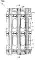
- FIGS. 1-2 show an organic EL display device 10 of the first embodiment.
- This organic EL display device 10 is used for, e.g., displays of portable information devices, full-color high-definition televisions, etc.
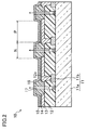
- the organic EL display device 10 is provided so that a substrate such as a TFT substrate 11 faces a sealing member.
- a planarizing film 12, a first electrode 13, an organic layer 14, and a second electrode 15 are sequentially stacked from the side of the TFT substrate 11 in the space formed between the TFT substrate 11 and the sealing member.
- the plurality of light-emitting regions P are arranged in a matrix pattern, and these light-emitting regions P are independently driven to display a predetermined image in the light-emitting regions P.
- a non-light-emitting region N where no light is emitted is formed around each light-emitting region P.
- the plurality of light-emitting regions P are comprised of three types of light-emitting regions P, namely red light-emitting regions P, green light-emitting regions P, and blue light-emitting regions P.
- the organic EL display device 10 is 400-500 mm long, 300-400 mm wide, and 1-30 mm thick.
- each of the light-emitting regions P is about 200 ⁇ m long and about 50 ⁇ m wide, and the light-emitting regions P are arranged at intervals of about 100 ⁇ m in the longitudinal direction and about 50 ⁇ m in the lateral direction.
- the TFT substrate 11 is configured so that TFTs 11b, interconnects 11c, etc. are formed on a TFT substrate main body 11a.
- the plurality of TFTs 11b are provided on the TFT substrate main body 11a at predetermined intervals (e.g., at intervals of about 300 ⁇ m in the longitudinal direction and about 100 ⁇ m in the lateral direction) corresponding to the pitch of the plurality of light-emitting regions P.
- the planarizing film 12 having an insulating property is formed so as to cover each of the plurality of TFTs 11b.
- the TFT substrate main body 11a is, e.g., an insulating substrate such as glass.
- the TFT substrate main body 11a is about 320 mm long, about 400 mm wide, and about 0.7 mm thick.
- Each of the TFTs 11b functions as a switching element in a corresponding one of the light-emitting regions P.
- the TFTs 11b are comprised of, e.g., an inorganic semiconductor material such as amorphous silicon or polysilicon, etc.
- the planarizing film 12 has a function to planarize stepped portions or concaves and convexes in the TFT substrate 11 so that the flat first electrodes 13 can be formed.
- the planarizing film 12 is comprised of, e.g., a photosensitive organic resin material such as an acrylic resin, a polyimide resin, or a novolak resin. Of these materials, the acrylic resin is preferable because it is inexpensive and is colorless and transparent.
- the planarizing film 12 is preferably comprised of a light transmitting material such as an acrylic resin because the TFT substrate 11 is required to have a light transmitting property.
- the planarizing film 12 has a thickness of, e.g., 0.5-5 ⁇ m, and is preferably 2 ⁇ m or more in order to more reliably ensure its flatness and electrically insulating property.
- the first electrode 13 is provided in each light-emitting region P so as to have an independent island pattern.
- Each of the first electrodes 13 is electrically connected to the TFT 11b in a corresponding one of the light-emitting regions P via a corresponding one of the contact holes 12c formed in the planarizing film 12.
- the island pattern of the first electrode 13 need only be formed so as to correspond to at least the light-emitting region P, a part of the island pattern of the first electrode 13 is formed in the non-light-emitting region N surrounding the light-emitting region P. In the non-light-emitting region N, the first electrode 13 is covered by an edge cover 16.
- each first electrode 13 has a thickness of, e.g., about 100 nm.
- Each of the first electrodes 13 has a function as an anode to inject holes into the organic layer 14.
- the anode is comprised of, e.g., an indium oxide-tin oxide alloy (ITO), an indium oxide-zinc oxide alloy (In 2 O 3 -ZnO), zinc oxide (ZnO), etc.
- ITO indium oxide-tin oxide alloy
- In 2 O 3 -ZnO indium oxide-zinc oxide alloy
- ZnO zinc oxide
- the organic EL display device 10 has a bottom emission structure configured to emit light from the side of the first electrodes 13
- the first electrodes 13 are comprised of a light-transmitting or semitransparent material.
- the first electrodes 13 are comprised of a light reflecting material.
- the edge cover 16 is provided on the first electrodes 13 in the non-light-emitting region N so as to cover the periphery of each first electrode 13. In a portion of the non-light emitting region N where the first electrode 13 does not extend, the edge cover 16 is provided on the planarizing film 12. That is, the edge cover 16 is formed so as to separate the islands of the first electrodes 13 in adjoining ones of the light-emitting regions P from each other. This can prevent electrical connection between adjoining ones of the islands of the first electrodes 13.
- the edge cover 16 is comprised of, e.g., an inorganic insulating material such as silicon dioxide (SiO 2 ), a silicon nitride film (SiN x ), a silicon oxide film (SiO x ), or a silicon oxynitride film (SiNO), or an organic resin such as an acrylic resin or a polyimide resin.
- the edge cover 16 has a height of, e.g., 0.5-2 ⁇ m.
- the edge cover 16 has holes 17 extending from the surface of the edge cover 16 to the planarizing film 12 and extending through the planarizing film 12, and the planarizing film 12 is exposed by the inner wall surfaces of the holes 17.
- Each of the holes 17 has a function to discharge water contained in the planarizing film 12 into the space in the hole 17 from the exposed portion of the planarizing film 12 on the inner wall surface of the hole 17. Since the space in the hole 17 communicates with the space formed between the TFT substrate 11 and the sealing member, the water discharged into the space in the hole 17 is absorbed by a desiccant or a moisture absorbent provided in the space formed between the TFT substrate 11 and the sealing member.
- each hole 17 has, e.g., a circular shape as viewed in plan.
- the hole 17 has a depth of about 3 ⁇ m and a diameter of about 5 ⁇ m.
- the surface of the TFT substrate 11 may be exposed at the bottom surface of the hole 17, or materials of the organic layer 14 and the second electrode 15 may be deposited on the bottom surface of the hole 17, as described later in the manufacturing method. It is preferable that the wall surface of the hole 17 extend perpendicularly to the TFT substrate 11. This can suppress adhesion of other materials to the inner wall of the hole 17 if they enter the hole 17 through the opening of the hole 17. As a result, the planarizing film 12 can be reliably exposed by the inner wall of the hole 17.
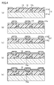
- the shape of the hole 17 is not limited to the circular shape as viewed in plan as shown in FIG. 1 .
- the hole 17 may have a rectangular shape, as shown in FIG. 3A .
- the area of the inner wall surface of the hole 17 serving as a discharge passage of the water can be increased by forming the hole 17 having a rectangular shape as viewed in plan.
- a plurality of holes 17 may be provided as shown in FIG. 3B or 3C , or the hole 17 may have a meandering shape as shown in FIG. 3D .
- the organic layer 14 includes at least a light-emitting layer.
- a hole injection layer, a hole transport layer, an electron blocking layer, etc. are provided on the hole injection side (the anode side), and an electron injection layer, an electron transport layer, a hole blocking layer, etc. are provided on the electron injection side (the cathode side).
- the organic layer 14 may have a three-layer structure formed by stacking the hole transport layer, the light-emitting layer, and the electron transport layer, or a five-layer structure formed by stacking the hole injection layer, the hole transport layer, the light-emitting layer, the electron transport layer, and the electron injection layer, or a six-layer structure formed by stacking the hole injection layer, the hole transport layer, the electron blocking layer, the light-emitting layer, the hole blocking layer, and the electron injection layer.
- the hole injection layer and the hole transport layer have a function to efficiently inject and transport holes received from the anode to the light-emitting layer.
- a hole injection material include copper phthalocyanine (CuPc) etc.
- a hole transport material include aromatic tertiary amines such as 4,4'-bis[N-(1-naphtyl)-N-phenylamino]biphenyl ( ⁇ -NPD).
- the hole injection layer and the hole transport layer have a thickness of about 30 nm and about 20 nm, respectively.
- the light-emitting layer has a function to emit light by recombination of holes and electrons respectively injected from the anode and the cathode in response to voltage application to the first electrode 13 and the second electrode 15.
- a light-emitting material include metal oxinoid compounds ((8-hydroxyquinoline) metal complex), naphthalene derivatives, anthracene derivatives, diphenylethylene derivatives, vinylacetone derivatives, triphenylamine derivatives, butadiene derivatives, coumarin derivatives, benzoxazole derivatives, oxadiazole derivatives, oxazole derivatives, benzimidazole derivatives, thiadiazole derivatives, perylene derivatives, perinone derivatives, rhodamine derivatives, phenoxazone, quinacridone derivatives, rubrene, poly(p-phenylenevinylene), polysilane, etc.
- the light-emitting layer has a thickness of, e.g.,
- the electron injection layer and the electron transport layer have a function to efficiently inject and transport electrons received from the cathode to the light-emitting layer.
- Examples of an electron transport material include tris(8-quinolinyloxy)aluminum (Alq3) etc.
- Examples of an electron injection material include lithium fluoride (LiF) etc.
- the electron transport layer and the electron injection layer have a thickness of about 30 nm and about 1 nm, respectively.
- the second electrode 15 has a function as a cathode to inject electrons into the organic layer 14.
- a material of the cathode include metal materials such as silver (Ag), aluminum (Al), vanadium (V), cobalt (Co), nickel (Ni), tungsten (W), gold (Au), calcium (Ca), titanium (Ti), yttrium (Y), sodium (Na), ruthenium (Ru), manganese (Mn), indium (In), magnesium (Mg), lithium (Li), and ytterbium (Yb), alloys such as lithium fluoride (LiF)/calcium (Ca)/aluminum (Al), etc.
- metal materials such as silver (Ag), aluminum (Al), vanadium (V), cobalt (Co), nickel (Ni), tungsten (W), gold (Au), calcium (Ca), titanium (Ti), yttrium (Y), sodium (Na), ruthenium (Ru), manganese (Mn), in
- the second electrode 15 is comprised of a light-reflecting material.
- the second electrode 15 is comprised of a light-transmitting or semitransparent material.
- the organic EL display device 10 may be an organic EL element having an inverted structure in which the first electrodes 13 function as a cathode and the second electrode 15 functions as an anode. In this case, the first electrodes 13 are comprised of a material of the cathode, and the second electrode 15 is comprised of a material of the anode.
- the sealing member is, e.g., a substrate comprised of glass etc., and has a desiccant bonded to its surface on the side of the TFT substrate 11 in the non-light-emitting region N.
- the sealing member is, e.g., 400-500 mm long, 300-400 mm wide, and 0.3-1.1 mm thick.
- the TFT substrate 11 is bonded to the sealing member by, e.g., a sealing resin such as an ultraviolet curable resin or a thermosetting epoxy resin.
- a sealing resin such as an ultraviolet curable resin or a thermosetting epoxy resin.
- the space sealed by the TFT substrate 11 and the sealing member is filled with inert gas such as dry argon or dry nitrogen.
- Polarizers may be provided on the outer surfaces of the TFT substrate 11 and the sealing member, respectively.
- the manufacturing method of the organic EL display device 10 includes a planarizing-film formation step, a first-electrode formation step, an edge-cover formation step, a hole formation step, an organic-layer/second-electrode formation step, and a sealing step. Note that the manufacturing method will be described with respect to an example in which the edge cover 16 is comprised of an inorganic insulating material such as SiO 2 .
- a plurality of TFTs 11b are formed at predetermined intervals on an insulating TFT substrate main body 11a by using a know method, and a planarizing film 12 is formed by using a photolithography technique.
- a substrate having a cleaned surface is coated with an acrylic resin by using a spin coating method, and the resultant substrate is prebaked at about 80°C for about 20 minutes to form an acrylic resin film.
- This acrylic resin film is exposed (e.g., about 360 mJ/cm 2 ) by using a photomask, and is developed by using tetramethylammonium hydroxide (TMAH) as a photoresist developer, thereby forming contact holes 12c electrically connected to the TFTs 11b.
- TMAH tetramethylammonium hydroxide
- Each of the contact holes 12c has a diameter of, e.g., 5 ⁇ m.
- postbake is performed at about 220°C for about one hour to form the planarizing film 12.
- first electrodes 13 are formed as shown in FIG. 4A .
- the first electrodes 13 are comprised of, e.g., ITO
- an ITO film having a thickness of about 100 nm is first formed by using a sputtering method, and the first electrodes 13 are formed so as to correspond to pixel regions by using a photolithography technique.
- the first electrodes 13 are electrically connected to the TFTs 11b via the contact holes 12c in the planarizing film 12.
- an edge cover 16 is patterned so as to cover peripheral portions of the first electrodes 13 in the non-light-emitting region N.
- an inorganic insulating material e.g., SiO 2
- the inorganic insulating material film is exposed and developed by using a photolithography technique, and then is dry etched (e.g., radio frequency (RF) power: 1,000 W, CF 4 /O 2 gas flow ratio: 425/75 [sccm/sccm], and etching time: 150-200 seconds) to form the edge cover 16 having a predetermined pattern.
- RF radio frequency
- the edge cover 16 thus patterned covers the peripheral portions of the first electrodes 13 in the non-light-emitting region N, and has, at predetermined positions in the non-light-emitting region N, holes 17a extending through the edge cover 16 and reaching the planarizing film 12.
- the planarizing film 12 is etched by using the pattern of the edge cover 16 having the holes 17a therein as a mask, thereby forming holes 17b extending from the edge cover 16 to the planarizing film 12.
- an organic layer 14 is formed by using a know method such as a resistance heating deposition method, an ion beam deposition method, or an inkjet method so that a predetermined organic layer 14 (e.g., an organic layer comprised of a red light-emitting organic EL material) is provided in a predetermined light-emitting region P (e.g., a red light-emitting region).
- a predetermined organic layer 14 e.g., an organic layer comprised of a red light-emitting organic EL material
- P e.g., a red light-emitting region
- this organic layer 14a does not affect the function of the organic EL element, and the organic layer 14 need not be patterned, whereby the manufacturing process can be simplified.
- a second electrode 15 is formed on the organic layer 14 by using a known method such as a sputtering method. At this time, the second electrode 15 is formed over the entire substrate. Like the organic layer 14, even if the material of the second electrode 15 is stacked on the bottoms of the holes 17 extending through both the edge cover 16 and the planarizing film 12, this second electrode 15a does not affect the performance of the organic EL display device, and the second electrode 15 need not be patterned, whereby the manufacturing process can be simplified.
- the TFT substrate 11 is placed so as to face a sealing member, and is bonded to the sealing member by using a sealing resin. Note that in the surface of sealing glass located on the side of the TFT substrate 11, a recess is formed in advance in a region that will serve as the non-light-emitting region N, and a desiccant is bonded in advance to the recess.
- the TFT substrate 11 it is preferable to bond the TFT substrate 11 to the sealing member in a glove box in order to perform this bonding under the conditions of a predetermined water concentration or less and a predetermined oxygen concentration or less.
- the glove box is filled with, e.g., inert gas such as nitrogen or argon, and the water concentration and the oxygen concentration in the glove box are preferably controlled to 10 ppm or less, and more preferably to 1 ppm or less.
- the organic EL display device 10 according to the first embodiment is obtained by the above steps.
- An organic EL display device 10 according to a second embodiment will be described below.
- the configurations corresponding to the organic EL display device 10 of the first embodiment are denoted by the same reference characters.
- FIG. 5 shows the organic EL display device 10 according to the second embodiment.
- the organic EL display device 10 is configured by sequentially stacking a planarizing film 12, first electrodes 13, an organic layer 14, and a second electrode 15 on a TFT substrate 11.
- the edge cover 16 has holes 17 extending from the surface of the edge cover 16 to the planarizing film 12, and the planarizing film 12 is exposed by the inner wall surfaces of the holes 17.
- the holes 17 extend to such a depth that the holes 17 do not extend through the planarizing film 12.
- Each of the holes 17 has a function to discharge water contained in the planarizing film 12 into the space in the hole 17 from the exposed portion of the planarizing film 12 on the inner wall surface of the hole 17. Since the space in the hole 17 communicates with the space formed between the TFT substrate 11 and a sealing member, the water discharged into the space in the hole 17 is absorbed by a desiccant or a moisture absorbent provided in the space formed between the TFT substrate 11 and the sealing member.
- a planarizing film 12 is formed over a TFT substrate 11, and contact holes 12c are formed in the planarizing film 12. Then, a first electrode 13 is patterned in each light-emitting region P so as to be electrically connected to a corresponding one of TFTs 11b.
- an edge cover 16 is patterned so as to cover peripheral portions of the first electrodes 13 by, e.g., a photolithography technique using a spin coating method.
- anisotropically etching the edge cover 16 and the planarizing film 12 by using, e.g., a reactive ion etching (RIE) method etc. allows the resultant holes 17 to have inner wall surfaces extending perpendicularly to the TFT substrate 11.
- the etching is performed under the following conditions. RF power: about 1,000 W, O 2 flow rate: about 300 sccm, bias voltage: about 500 V, and etching time: about 300 seconds. Since the holes 17 having the inner wall surfaces extending perpendicularly to the TFT substrate 11 are formed by using the anisotropic etching, adhesion of other materials to the inner wall surfaces of the holes 17 is suppressed in the manufacturing process after the formation of the holes 17.
- the planarizing film 12 can be reliably exposed by the inner walls of the holes 17, and a flow passage for discharging water contained in the planarizing film 12 to the outside can be obtained.
- the edge cover 16 in the case where the edge cover 16 is comprised of an organic resin, the edge cover 16 also contains water. However, since the holes 17 are formed to extend from the second electrode 15 and through the edge cover 16 to the planarizing film 12, a part of the edge cover 16 is exposed is exposed by the inner wall surfaces of the holes 17. This suppresses entrance of the water contained in the organic resin of the edge cover 16 into the organic layer 14 or the electrodes, and thus can suppress degradation in organic EL luminous characteristics by the water contained in the edge cover 16.
- the holes 17 are formed so as to extend to a depth that is shallower than the entire depth of the planarizing film 12 in the hole formation step. This can reduce the etching time required to form the holes 17.
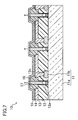
- FIG. 7 shows the organic EL display device 10 according to the third embodiment.
- the organic EL display device 10 is configured by sequentially stacking a planarizing film 12, first electrodes 13, an organic layer 14, and a second electrode 15 on a TFT substrate 11.
- the edge cover 16 has holes 17 extending from the surface of the edge cover 16 to the planarizing film 12 and extending through the planarizing film 12, and the planarizing film 12 is exposed by the inner wall surfaces of the holes 17.
- a coating film 12a which is comprised of the same material (e.g., an inorganic insulating material or an organic resin) as the edge cover 16, is formed on the exposed surfaces of the planarizing film 12, and the coating film 12a is integral with the edge cover 16.
- Each of the holes 17 has a function to discharge water contained in the planarizing film 12 into the space in the hole 17 from the exposed portion of the planarizing film 12 on the inner wall surface of the hole 17.
- the space in the hole 17 communicates with the space formed between the TFT substrate 11 and a sealing member, the water discharged into the space in the hole 17 is absorbed by a desiccant or a moisture absorbent provided in the space formed between the TFT substrate 11 and the sealing member.
- each hole 17 has, e.g., a circular shape as viewed in plan.
- the hole 17 has a depth of about 3 ⁇ m and a diameter of about 5 ⁇ m.
- the coating film 12a may be formed in the entire exposed portion of the planarizing film 12 on the inner wall surface of each hole 17, or may be formed in a part of the exposed surface of the planarizing film 12 on the inner wall surface of each hole 17.
- the coating film 12a has a thickness of, e.g., about 200 nm.
- This manufacturing method of the organic EL display device 10 includes a planarizing-film formation step, a first-electrode formation step, a hole formation step, an edge-cover formation step, an organic-layer/second-electrode formation step, and a sealing step.
- a planarizing film 12 is formed over a TFT substrate 11, and contact holes 12c are formed in the planarizing film 12. Then, a first electrode 13 is patterned in each light-emitting region P so as to be electrically connected to a corresponding one of TFTs 11b.
- the planarizing film 12 is etched in a non-light-emitting region N to form the holes 17.
- anisotropically etching the planarizing film 12 by using, e.g., a reactive ion etching (RIE) method etc. allows the resultant holes 17 to have inner wall surfaces extending perpendicularly to the TFT substrate 11.
- RIE reactive ion etching
- an edge cover 16 is patterned so as to cover peripheral portions of the first electrodes 13 in the non-light-emitting region N.
- an inorganic insulating material (e.g., SiO 2 ) film is formed with a thickness of about 150 nm by using a sputtering method etc.
- the inorganic insulating material film is exposed and developed by using a photolithography technique, and then is dry etched (e.g., RF power: 1,000 W, CF 4 /O 2 gas flow ratio: 425/75 [sccm/sccm], and etching time: 150-200 seconds) to form the edge cover 16 having a predetermined pattern.
- an organic layer 14 and a second electrode 15 are sequentially formed as in the first embodiment.
- the TFT substrate 11 is placed so as to face a sealing member, and is bonded to the sealing member.
- the organic EL display device 10 according to the third embodiment is obtained in this manner.
- the holes 17 extending from the second electrode 15 to the planarizing film 12 are formed in the non-light-emitting region N, and at least the planarizing film 12 is exposed by the inner wall surfaces of the holes 17.
- water contained in the organic resin of the planarizing film 12 is discharged from the inner wall surfaces of the holes 17 to the outside. This suppresses entrance of the water contained in the organic resin of the planarizing film 12 into the organic layer 14 or the electrodes, and thus can suppress degradation in organic EL luminous characteristics by the water contained in the planarizing film 12.
- the coating film 12a does not hinder discharge of the water from the exposed portions of the planarizing film 12, and the effect of suppressing degradation in organic EL luminous characteristics can be sufficiently achieved.
- the present invention is useful for organic EL devices such as organic EL display devices.
Abstract
Description
- The present invention relates to organic electroluminescence (EL) devices in which degradation in organic EL luminous characteristics is suppressed.
- In recent years, with diversification of information processing apparatuses, there has been a growing demand for flat panel displays having lower power consumption than cathode ray tubes (CRTs) and capable of being reduced in thickness. An organic EL panel is an example of flat panel displays that are advantageous in terms of low voltage drive, all-solid-state type, high-speed response, self light emission, etc. In an organic EL panel, thin film transistors (hereinafter referred to as the "TFTs") are provided on, e.g., a glass substrate, a planarizing film is provided to planarize and insulate the substrate surface, and a first electrode, an organic layer, and a second electrode are sequentially stacked on the planarizing film.
- The planarizing film is comprised of an organic resin material such as an acrylic resin or a polyimide resin, in view of the dielectric constant, the film thickness, easiness of planarization, easiness of patterning control, easiness of control of the taper angle at the end of a formed pattern. In particular, the acrylic resin is more advantageous than the polyimide resin in terms of the cost and in terms of the fact that the acrylic resin is a colorless, transparent resin while the polyimide resin is a colored, transparent resin. Thus, the acrylic resin is preferably used as the planarizing film.
- These organic resin materials tend to accumulate water, oxygen, etc. therein as compared to materials comprised of an inorganic compound. In particular, the acrylic resin is more hygroscopic than the polyamide resin, and contains a larger amount of water than the polyamide resin. The water contained in the organic resin can be removed in advance by baking. However, for example, since the acrylic resin can resist heat up to about 250°C, the water contained in the acrylic resin cannot be sufficiently removed by the baking performed at a temperature lower than about 250°C. Thus, in the case where the planarizing film is comprised of the organic resin material, water etc. leaks from the planarizing film, and outgas from the planarizing film reaches the electrodes or the organic layer. Accordingly, the peripheral portions of the electrodes or the organic layer are damaged, and luminance is reduced in the degraded portions.
- Patent Document 1 discloses a configuration in which inorganic insulating films are respectively provided in the layers located above and below a planarizing film comprised of an organic material. According to Patent Document 1, since the planarizing film is completely covered by the inorganic insulating films, the planarizing film can be prevented from absorbing water during manufacturing of an organic EL device, and degradation of the organic layer by the water can be prevented.
- Patent Document 2 discloses an organic EL panel having a configuration in which a planarizing film is divided on a pixel-by-pixel basis by a planarizing-film dividing portion provided in a display region. According to this configuration, even if water leaks from the planarizing film in any of the pixels, the water is not allowed to move to the planarizing films in the other pixels, whereby the water leaking from the polarizing film can be prevented from diffusing in the entire display region.
-
- PATENT DOCUMENT 1: Japanese Patent Publication No.
2007-121537 - PATENT DOCUMENT 2: Japanese Patent Publication No.
2005-164818 - However, the organic EL device having the configuration of Patent Document 1 typically does not have satisfactory adhesion between the organic film and the inorganic films, film delamination or cracks may occur during the manufacturing process or while the product is in use. If the inorganic insulating film is damaged (film delamination, cracks, pinholes produced by other causes, etc.), water contained in the planarizing film leaks from the damaged portion. That is, the organic EL device having the configuration of Patent Document 1 does not satisfactorily solve the problems regarding leakage of water etc. contained in the acrylic resin and degradation in organic EL luminous characteristics by outgas from the acrylic resin.
- According to the organic EL panel having the configuration of Patent Document 2, the planarizing-film dividing portion can prevent the water contained in each planarizing film from moving in the entire display region. However, since the surface of each of the divided planarizing films is covered by an inorganic film as a pixel electrode, the water is kept in the planarizing films. Thus, the organic EL characteristics can be degraded after long-term use of the organic EL panel due to damage to the pixel electrodes by the water leaking from the planarizing films.
- It is an object of the present invention to suppress degradation in organic EL luminous characteristics due to leakage of water etc. contained in an organic resin of a planarizing film etc. with time.
- An organic EL device according to the present invention is an organic EL device having a light-emitting region and a non-light-emitting region located outside the light-emitting region, and including: a substrate; a planarizing film comprised of an organic resin and provided over the substrate so as to cover the light-emitting region and the non-light-emitting region; a first electrode provided on the planarizing film so as to cover at least the light-emitting region; an organic layer provided on the first electrode so as to cover at least the light-emitting region; and a second electrode provided on the organic layer so as to cover the light-emitting region and the non-light-emitting region, wherein a hole is formed in the non-light-emitting region so as to extend from the second electrode to the planarizing film, and at least the planarizing film is exposed by an inner wall surface of the hole.
- With the above configuration, the hole extending from the second electrode to the planarizing film is formed in the non-light-emitting region, and at least the planarizing film is exposed by the inner wall surface of the hole. Thus, water contained in the organic resin of the planarizing film is discharged to the outside from the inner wall surface of the hole. This suppresses entrance of the water contained in the organic resin of the planarizing film to the organic film or the electrodes, and thus can suppress degradation in organic EL luminous characteristics by the water contained in the planarizing film.
- In the organic EL device of the present invention, it is preferable that the first electrode be provided so as to cover a part of the non-light-emitting region as well, and that the organic EL device further include: an edge cover provided in the non-light-emitting region so as to cover the first electrode and the planarizing film.
- In the organic EL device of the present invention, it is preferable that the hole be formed so as to extend through the planarizing film.
- With the above configuration, since the hole is formed so as to extend through the planarizing film, the area of the exposed portion of the planarizing film on the inner wall surface of the hole can be increased, and a large flow passage for discharging the water contained in the planarizing film to the outside can be obtained.
- In the present invention, it is preferable that the inner wall surface of the hole extend perpendicularly to the substrate.
- With the above configuration, the inner wall surface of the hole extends perpendicularly to the substrate. This can suppress adhesion of materials of the organic layer, the second electrode, etc., which are to be formed after formation of the hole, to the inner wall of the hole when forming the organic layer, the second electrode, etc. in the manufacturing process of the organic EL device. As a result, the planarizing film can be reliably exposed by the inner wall of the hole, and a flow passage for discharging the water contained in the planarizing film to the outside can be obtained.
- In the present invention, the planarizing film may have a thickness of 2-5 µm.
- With the above configuration, since the thickness of the planarizing film is 2 µm or more, flatness and an electrically insulating property of the substrate surface can be sufficiently ensured.
- In the organic EL device of the present invention, the planarizing film exposed by the inner wall surface of the hole may be covered by a coating film, which is comprised of a same material as the edge cover and is formed integrally with the edge cover.
- In the present invention, the hole may have a circular shape as viewed in plan.
- The hole may have a rectangular shape as viewed in plan.
- With the above configuration, since the hole has a rectangular shape as viewed in plan, the area of the inner wall surface of the hole can be increased as compared to the case where the hole has a circular shape as viewed in plan, whereby a large flow passage of the water can be obtained.
- In the present invention, the planarizing film may be comprised of a polyimide resin or an acrylic resin.
- The organic EL device of the present invention may be used in a display application.
- According to the organic EL device of the present invention, the hole extending from the second electrode to the planarizing film is formed in the non-light-emitting region, and at least the planarizing film is exposed by the inner wall surface of the hole. Thus, water contained in the organic resin of the planarizing film is discharged to the outside from the inner wall surface of the hole. This suppresses entrance of the water contained in the organic resin of the planarizing film to the organic film or the electrodes, and thus can suppress degradation in organic EL luminous characteristics by the water contained in the planarizing film.
-
- [
FIG. 1] FIG. 1 is a plan view of an organic EL display device according to a first embodiment. - [
FIG. 2] FIG. 2 is a cross-sectional view taken along line II-II inFIG. 1 . - [
FIG. 3] FIGS. 3A-3D are diagrams showing modifications of the shape of holes. - [
FIG. 4] FIGS. 4A-4E are illustrations showing a manufacturing method of the organic EL display device according to the first embodiment. - [
FIG. 5] FIG. 5 is a cross-sectional view of an organic EL display device according to a second embodiment. - [
FIG. 6] FIGS. 6A-6D are illustrations showing a manufacturing method of the organic EL display device according to the second embodiment. - [
FIG. 7] FIG. 7 is a cross-sectional view of an organic EL display device according to a third embodiment. - [
FIG. 8] FIGS. 8A-8D are illustrations showing a manufacturing method of the organic EL display device according to the third embodiment. -
FIGS. 1-2 show an organicEL display device 10 of the first embodiment. This organicEL display device 10 is used for, e.g., displays of portable information devices, full-color high-definition televisions, etc. - The organic
EL display device 10 is provided so that a substrate such as aTFT substrate 11 faces a sealing member. In each light-emitting region P where the organicEL display device 10 emits light, aplanarizing film 12, afirst electrode 13, anorganic layer 14, and asecond electrode 15 are sequentially stacked from the side of theTFT substrate 11 in the space formed between theTFT substrate 11 and the sealing member. The plurality of light-emitting regions P are arranged in a matrix pattern, and these light-emitting regions P are independently driven to display a predetermined image in the light-emitting regions P. A non-light-emitting region N where no light is emitted is formed around each light-emitting region P. In the case where the organicEL display device 10 provides RGB full-color display, the plurality of light-emitting regions P are comprised of three types of light-emitting regions P, namely red light-emitting regions P, green light-emitting regions P, and blue light-emitting regions P. For example, the organicEL display device 10 is 400-500 mm long, 300-400 mm wide, and 1-30 mm thick. For example, each of the light-emitting regions P is about 200 µm long and about 50 µm wide, and the light-emitting regions P are arranged at intervals of about 100 µm in the longitudinal direction and about 50 µm in the lateral direction. - The
TFT substrate 11 is configured so thatTFTs 11b,interconnects 11c, etc. are formed on a TFT substratemain body 11a. The plurality ofTFTs 11b are provided on the TFT substratemain body 11a at predetermined intervals (e.g., at intervals of about 300 µm in the longitudinal direction and about 100 µm in the lateral direction) corresponding to the pitch of the plurality of light-emitting regions P. Theplanarizing film 12 having an insulating property is formed so as to cover each of the plurality ofTFTs 11b. - The TFT substrate
main body 11a is, e.g., an insulating substrate such as glass. For example, the TFT substratemain body 11a is about 320 mm long, about 400 mm wide, and about 0.7 mm thick. - Each of the TFTs 11b functions as a switching element in a corresponding one of the light-emitting regions P. The TFTs 11b are comprised of, e.g., an inorganic semiconductor material such as amorphous silicon or polysilicon, etc.
- The
planarizing film 12 has a function to planarize stepped portions or concaves and convexes in theTFT substrate 11 so that the flatfirst electrodes 13 can be formed. Theplanarizing film 12 is comprised of, e.g., a photosensitive organic resin material such as an acrylic resin, a polyimide resin, or a novolak resin. Of these materials, the acrylic resin is preferable because it is inexpensive and is colorless and transparent. In the case where an organic EL panel has a bottom emission structure, theplanarizing film 12 is preferably comprised of a light transmitting material such as an acrylic resin because theTFT substrate 11 is required to have a light transmitting property. Contact holes 12c are provided in theplanarizing film 12 so as to correspond to the plurality ofTFTs 11b, respectively. This allows the surface of the TFT substratemain body 11a to be electrically connected to theTFTs 11b. Theplanarizing film 12 has a thickness of, e.g., 0.5-5 µm, and is preferably 2 µm or more in order to more reliably ensure its flatness and electrically insulating property. - A TFT substrate having a planarizing film for use in liquid crystal devices may be used as the
TFT substrate 11 having its surface covered by theplanarizing film 12. - The
first electrode 13 is provided in each light-emitting region P so as to have an independent island pattern. Each of thefirst electrodes 13 is electrically connected to theTFT 11b in a corresponding one of the light-emitting regions P via a corresponding one of thecontact holes 12c formed in theplanarizing film 12. Although the island pattern of thefirst electrode 13 need only be formed so as to correspond to at least the light-emitting region P, a part of the island pattern of thefirst electrode 13 is formed in the non-light-emitting region N surrounding the light-emitting region P. In the non-light-emitting region N, thefirst electrode 13 is covered by anedge cover 16. That is, a peripheral portion of the island pattern of eachfirst electrode 13 is covered by theedge cover 16, and the islands of adjoining ones of thefirst electrodes 13 are separated from each other by theedge cover 16. Each of thefirst electrodes 13 has a thickness of, e.g., about 100 nm. - Each of the
first electrodes 13 has a function as an anode to inject holes into theorganic layer 14. The anode is comprised of, e.g., an indium oxide-tin oxide alloy (ITO), an indium oxide-zinc oxide alloy (In2O3-ZnO), zinc oxide (ZnO), etc. In the case where the organicEL display device 10 has a bottom emission structure configured to emit light from the side of thefirst electrodes 13, thefirst electrodes 13 are comprised of a light-transmitting or semitransparent material. In the case where the organicEL display device 10 has a top emission structure configured to emit light from the side of thesecond electrode 15, thefirst electrodes 13 are comprised of a light reflecting material. - The
edge cover 16 is provided on thefirst electrodes 13 in the non-light-emitting region N so as to cover the periphery of eachfirst electrode 13. In a portion of the non-light emitting region N where thefirst electrode 13 does not extend, theedge cover 16 is provided on theplanarizing film 12. That is, theedge cover 16 is formed so as to separate the islands of thefirst electrodes 13 in adjoining ones of the light-emitting regions P from each other. This can prevent electrical connection between adjoining ones of the islands of thefirst electrodes 13. Theedge cover 16 is comprised of, e.g., an inorganic insulating material such as silicon dioxide (SiO2), a silicon nitride film (SiNx), a silicon oxide film (SiOx), or a silicon oxynitride film (SiNO), or an organic resin such as an acrylic resin or a polyimide resin. Theedge cover 16 has a height of, e.g., 0.5-2 µm. - The
edge cover 16 hasholes 17 extending from the surface of theedge cover 16 to theplanarizing film 12 and extending through theplanarizing film 12, and theplanarizing film 12 is exposed by the inner wall surfaces of theholes 17. Each of theholes 17 has a function to discharge water contained in theplanarizing film 12 into the space in thehole 17 from the exposed portion of theplanarizing film 12 on the inner wall surface of thehole 17. Since the space in thehole 17 communicates with the space formed between theTFT substrate 11 and the sealing member, the water discharged into the space in thehole 17 is absorbed by a desiccant or a moisture absorbent provided in the space formed between theTFT substrate 11 and the sealing member. - The opening of each
hole 17 has, e.g., a circular shape as viewed in plan. For example, thehole 17 has a depth of about 3 µm and a diameter of about 5 µm. The surface of theTFT substrate 11 may be exposed at the bottom surface of thehole 17, or materials of theorganic layer 14 and thesecond electrode 15 may be deposited on the bottom surface of thehole 17, as described later in the manufacturing method. It is preferable that the wall surface of thehole 17 extend perpendicularly to theTFT substrate 11. This can suppress adhesion of other materials to the inner wall of thehole 17 if they enter thehole 17 through the opening of thehole 17. As a result, theplanarizing film 12 can be reliably exposed by the inner wall of thehole 17. - The shape of the
hole 17 is not limited to the circular shape as viewed in plan as shown inFIG. 1 . For example, thehole 17 may have a rectangular shape, as shown inFIG. 3A . The area of the inner wall surface of thehole 17 serving as a discharge passage of the water can be increased by forming thehole 17 having a rectangular shape as viewed in plan. A plurality ofholes 17 may be provided as shown inFIG. 3B or 3C , or thehole 17 may have a meandering shape as shown inFIG. 3D . By increasing the area of the inner wall surface of thehole 17, a larger flow passage for discharging water contained in the organic resin to the outside can be obtained. - The
organic layer 14 includes at least a light-emitting layer. A hole injection layer, a hole transport layer, an electron blocking layer, etc. are provided on the hole injection side (the anode side), and an electron injection layer, an electron transport layer, a hole blocking layer, etc. are provided on the electron injection side (the cathode side). Theorganic layer 14 may have a three-layer structure formed by stacking the hole transport layer, the light-emitting layer, and the electron transport layer, or a five-layer structure formed by stacking the hole injection layer, the hole transport layer, the light-emitting layer, the electron transport layer, and the electron injection layer, or a six-layer structure formed by stacking the hole injection layer, the hole transport layer, the electron blocking layer, the light-emitting layer, the hole blocking layer, and the electron injection layer. - The hole injection layer and the hole transport layer have a function to efficiently inject and transport holes received from the anode to the light-emitting layer. Examples of a hole injection material include copper phthalocyanine (CuPc) etc. Examples of a hole transport material include aromatic tertiary amines such as 4,4'-bis[N-(1-naphtyl)-N-phenylamino]biphenyl (α-NPD). The hole injection layer and the hole transport layer have a thickness of about 30 nm and about 20 nm, respectively.
- The light-emitting layer has a function to emit light by recombination of holes and electrons respectively injected from the anode and the cathode in response to voltage application to the
first electrode 13 and thesecond electrode 15. Examples of a light-emitting material include metal oxinoid compounds ((8-hydroxyquinoline) metal complex), naphthalene derivatives, anthracene derivatives, diphenylethylene derivatives, vinylacetone derivatives, triphenylamine derivatives, butadiene derivatives, coumarin derivatives, benzoxazole derivatives, oxadiazole derivatives, oxazole derivatives, benzimidazole derivatives, thiadiazole derivatives, perylene derivatives, perinone derivatives, rhodamine derivatives, phenoxazone, quinacridone derivatives, rubrene, poly(p-phenylenevinylene), polysilane, etc. The light-emitting layer has a thickness of, e.g., about 20 nm. - The electron injection layer and the electron transport layer have a function to efficiently inject and transport electrons received from the cathode to the light-emitting layer. Examples of an electron transport material include tris(8-quinolinyloxy)aluminum (Alq3) etc. Examples of an electron injection material include lithium fluoride (LiF) etc. The electron transport layer and the electron injection layer have a thickness of about 30 nm and about 1 nm, respectively.
- The
second electrode 15 is formed so as to cover the entire substrate, namely so as to cover theorganic layer 14 in the light-emitting regions P and theedge cover 16 and the film of theorganic layer 14 adhering to theedge cover 16 in the non-light-emitting region N. Thesecond electrode 15 has a thickness of, e.g., about 10-200 nm. - The
second electrode 15 has a function as a cathode to inject electrons into theorganic layer 14. Examples of a material of the cathode include metal materials such as silver (Ag), aluminum (Al), vanadium (V), cobalt (Co), nickel (Ni), tungsten (W), gold (Au), calcium (Ca), titanium (Ti), yttrium (Y), sodium (Na), ruthenium (Ru), manganese (Mn), indium (In), magnesium (Mg), lithium (Li), and ytterbium (Yb), alloys such as lithium fluoride (LiF)/calcium (Ca)/aluminum (Al), etc. In the case where the organicEL display device 10 has a bottom emission structure configured to emit light from the side of thefirst electrodes 13, thesecond electrode 15 is comprised of a light-reflecting material. In the case where the organicEL display device 10 has a top emission structure configured to emit light from the side of thesecond electrode 15, thesecond electrode 15 is comprised of a light-transmitting or semitransparent material. The organicEL display device 10 may be an organic EL element having an inverted structure in which thefirst electrodes 13 function as a cathode and thesecond electrode 15 functions as an anode. In this case, thefirst electrodes 13 are comprised of a material of the cathode, and thesecond electrode 15 is comprised of a material of the anode. - The sealing member is, e.g., a substrate comprised of glass etc., and has a desiccant bonded to its surface on the side of the
TFT substrate 11 in the non-light-emitting region N. The sealing member is, e.g., 400-500 mm long, 300-400 mm wide, and 0.3-1.1 mm thick. - The
TFT substrate 11 is bonded to the sealing member by, e.g., a sealing resin such as an ultraviolet curable resin or a thermosetting epoxy resin. The space sealed by theTFT substrate 11 and the sealing member is filled with inert gas such as dry argon or dry nitrogen. - Polarizers may be provided on the outer surfaces of the
TFT substrate 11 and the sealing member, respectively. - A manufacturing method of the organic
EL display device 10 according to the first embodiment will be described with reference toFIGS. 4A-4E . The manufacturing method of the organicEL display device 10 includes a planarizing-film formation step, a first-electrode formation step, an edge-cover formation step, a hole formation step, an organic-layer/second-electrode formation step, and a sealing step. Note that the manufacturing method will be described with respect to an example in which theedge cover 16 is comprised of an inorganic insulating material such as SiO2. - First, a plurality of
TFTs 11b are formed at predetermined intervals on an insulating TFT substratemain body 11a by using a know method, and aplanarizing film 12 is formed by using a photolithography technique. Specifically, for example, a substrate having a cleaned surface is coated with an acrylic resin by using a spin coating method, and the resultant substrate is prebaked at about 80°C for about 20 minutes to form an acrylic resin film. This acrylic resin film is exposed (e.g., about 360 mJ/cm2) by using a photomask, and is developed by using tetramethylammonium hydroxide (TMAH) as a photoresist developer, thereby formingcontact holes 12c electrically connected to theTFTs 11b. Each of thecontact holes 12c has a diameter of, e.g., 5 µm. Lastly, postbake is performed at about 220°C for about one hour to form theplanarizing film 12. - Next,
first electrodes 13 are formed as shown inFIG. 4A . In the case where thefirst electrodes 13 are comprised of, e.g., ITO, an ITO film having a thickness of about 100 nm is first formed by using a sputtering method, and thefirst electrodes 13 are formed so as to correspond to pixel regions by using a photolithography technique. At this time, thefirst electrodes 13 are electrically connected to theTFTs 11b via the contact holes 12c in theplanarizing film 12. - Then, as shown in
FIG. 4B , anedge cover 16 is patterned so as to cover peripheral portions of thefirst electrodes 13 in the non-light-emitting region N. First, an inorganic insulating material (e.g., SiO2) film is formed with a thickness of about 150 nm by using a sputtering method etc. The inorganic insulating material film is exposed and developed by using a photolithography technique, and then is dry etched (e.g., radio frequency (RF) power: 1,000 W, CF4/O2 gas flow ratio: 425/75 [sccm/sccm], and etching time: 150-200 seconds) to form theedge cover 16 having a predetermined pattern. - The
edge cover 16 thus patterned covers the peripheral portions of thefirst electrodes 13 in the non-light-emitting region N, and has, at predetermined positions in the non-light-emitting region N, holes 17a extending through theedge cover 16 and reaching theplanarizing film 12. - Subsequently, as shown in
FIG. 4C , theplanarizing film 12 is etched by using the pattern of theedge cover 16 having theholes 17a therein as a mask, thereby forming holes 17b extending from theedge cover 16 to theplanarizing film 12. - At this time, anisotropically etching the
planarizing film 12 by using, e.g., a reactive ion etching (RIE) method etc. allows theresultant holes 17 to have inner wall surfaces extending perpendicularly to aTFT substrate 11. For example, the etching is performed under the following conditions. RF power: about 1,000 W, O2 flow rate: about 300 sccm, bias voltage: about 500 V, and etching time: about 300 seconds. Since theholes 17 having the inner wall surfaces extending perpendicularly to theTFT substrate 11 are formed by using the anisotropic etching, adhesion of other materials to the inner wall surfaces of theholes 17 is suppressed in the manufacturing process after the formation of theholes 17. Thus, theplanarizing film 12 can be reliably exposed by the inner walls of theholes 17, and a flow passage for discharging water contained in theplanarizing film 12 to the outside can be obtained. - Thereafter, as shown in
FIG. 4D , anorganic layer 14 is formed by using a know method such as a resistance heating deposition method, an ion beam deposition method, or an inkjet method so that a predetermined organic layer 14 (e.g., an organic layer comprised of a red light-emitting organic EL material) is provided in a predetermined light-emitting region P (e.g., a red light-emitting region). At this time, performance of the organic EL display device is not affected even if theorganic layer 14 adheres to the non-light-emitting region N. Moreover, even if the material of theorganic layer 14 is stacked on the bottoms of theholes 17 extending from theedge cover 16 to theplanarizing film 12, thisorganic layer 14a does not affect the function of the organic EL element, and theorganic layer 14 need not be patterned, whereby the manufacturing process can be simplified. - Then, as shown in
FIG. 4E , asecond electrode 15 is formed on theorganic layer 14 by using a known method such as a sputtering method. At this time, thesecond electrode 15 is formed over the entire substrate. Like theorganic layer 14, even if the material of thesecond electrode 15 is stacked on the bottoms of theholes 17 extending through both theedge cover 16 and theplanarizing film 12, thissecond electrode 15a does not affect the performance of the organic EL display device, and thesecond electrode 15 need not be patterned, whereby the manufacturing process can be simplified. - Lastly, the
TFT substrate 11 is placed so as to face a sealing member, and is bonded to the sealing member by using a sealing resin. Note that in the surface of sealing glass located on the side of theTFT substrate 11, a recess is formed in advance in a region that will serve as the non-light-emitting region N, and a desiccant is bonded in advance to the recess. - It is preferable to bond the
TFT substrate 11 to the sealing member in a glove box in order to perform this bonding under the conditions of a predetermined water concentration or less and a predetermined oxygen concentration or less. The glove box is filled with, e.g., inert gas such as nitrogen or argon, and the water concentration and the oxygen concentration in the glove box are preferably controlled to 10 ppm or less, and more preferably to 1 ppm or less. - The organic
EL display device 10 according to the first embodiment is obtained by the above steps. - According to the organic
EL display device 10 of the first embodiment, theholes 17 extending from thesecond electrode 15 to theplanarizing film 12 are formed in the non-light-emitting region N, and at least theplanarizing film 12 is exposed by the inner wall surfaces of theholes 17. Thus, water contained in the organic resin of theplanarizing film 12 is discharged from the inner wall surfaces of theholes 17 to the outside. This suppresses entrance of the water contained in the organic resin of theplanarizing film 12 into theorganic layer 14 or the electrodes, and thus can suppress degradation in organic EL luminous characteristics by the water contained in theplanarizing film 12. - Moreover, forming the
holes 17 extending through theplanarizing film 12 can increase the area of the exposed surface of theplanarizing film 12 in the inner wall surfaces of theholes 17, whereby a large flow passage for discharging the water contained in theplanarizing film 12 to the outside can be obtained. - Furthermore, in the manufacturing process of the organic
EL display device 10, in the case where theedge cover 16 is comprised of an inorganic insulating material, theholes 17 can be formed by etching theplanarizing film 12 by using the pattern of theholes 17a formed in theedge cover 16 as a mask. This can simplify the manufacturing process. - An organic
EL display device 10 according to a second embodiment will be described below. The configurations corresponding to the organicEL display device 10 of the first embodiment are denoted by the same reference characters. -
FIG. 5 shows the organicEL display device 10 according to the second embodiment. - As in the first embodiment, the organic
EL display device 10 is configured by sequentially stacking aplanarizing film 12,first electrodes 13, anorganic layer 14, and asecond electrode 15 on aTFT substrate 11. - Since the configurations of the
TFT substrate 11, theplanarizing film 12, thefirst electrodes 13, and anedge cover 16 are similar to those of the first embodiment, description thereof will be omitted. - The
edge cover 16 hasholes 17 extending from the surface of theedge cover 16 to theplanarizing film 12, and theplanarizing film 12 is exposed by the inner wall surfaces of theholes 17. Theholes 17 extend to such a depth that theholes 17 do not extend through theplanarizing film 12. Each of theholes 17 has a function to discharge water contained in theplanarizing film 12 into the space in thehole 17 from the exposed portion of theplanarizing film 12 on the inner wall surface of thehole 17. Since the space in thehole 17 communicates with the space formed between theTFT substrate 11 and a sealing member, the water discharged into the space in thehole 17 is absorbed by a desiccant or a moisture absorbent provided in the space formed between theTFT substrate 11 and the sealing member. - The opening of each
hole 17 has, e.g., a circular shape as viewed in plan. For example, thehole 17 has a depth of about 3 µm and a diameter of about 5 µm. Theplanarizing film 12 may be exposed at the bottom surface of thehole 17, or materials of theorganic layer 14 and thesecond electrode 15 may be deposited on the bottom surface of thehole 17. - Since the configurations of the
organic layer 14, thesecond electrode 15, the sealing member, and the sealing structure between theTFT substrate 11 and the sealing member are also similar to those of the first embodiment, description thereof will be omitted. - A manufacturing method of the organic
EL display device 10 according to the second embodiment will be described with reference toFIGS. 6A-6D . As in the first embodiment, this manufacturing method includes a planarizing-film formation step, a first-electrode formation step, an edge-cover formation step, a hole formation step, an organic-layer/second-electrode formation step, and a sealing step. Note that the manufacturing method will be described with respect to an example in which theedge cover 16 is comprised of an organic resin such as SiO2. - First, as in the first embodiment, a
planarizing film 12 is formed over aTFT substrate 11, andcontact holes 12c are formed in theplanarizing film 12. Then, afirst electrode 13 is patterned in each light-emitting region P so as to be electrically connected to a corresponding one ofTFTs 11b. - Next, as shown in
FIG. 6A , anedge cover 16 is patterned so as to cover peripheral portions of thefirst electrodes 13 by, e.g., a photolithography technique using a spin coating method. - Then, as shown in
FIG. 6B , by using a mask formed so as to cover theedge cover 16 and thefirst electrodes 13, theedge cover 16 and theplanarizing film 12 are simultaneously etched to form holes 17. - At this time, anisotropically etching the
edge cover 16 and theplanarizing film 12 by using, e.g., a reactive ion etching (RIE) method etc. allows theresultant holes 17 to have inner wall surfaces extending perpendicularly to theTFT substrate 11. For example, the etching is performed under the following conditions. RF power: about 1,000 W, O2 flow rate: about 300 sccm, bias voltage: about 500 V, and etching time: about 300 seconds. Since theholes 17 having the inner wall surfaces extending perpendicularly to theTFT substrate 11 are formed by using the anisotropic etching, adhesion of other materials to the inner wall surfaces of theholes 17 is suppressed in the manufacturing process after the formation of theholes 17. Thus, theplanarizing film 12 can be reliably exposed by the inner walls of theholes 17, and a flow passage for discharging water contained in theplanarizing film 12 to the outside can be obtained. - Thereafter, as shown in
FIGS. 6C-6D , anorganic layer 14 and asecond electrode 15 are sequentially formed as in the first embodiment. Lastly, as in the first embodiment, theTFT substrate 11 is placed so as to face a sealing member, and is bonded to the sealing member by using a sealing resin. The organicEL display device 10 according to the second embodiment is obtained in this manner. - According to the organic
EL display device 10 of the second embodiment, theholes 17 extending from thesecond electrode 15 to theplanarizing film 12 are formed in the non-light-emitting region N, and at least theplanarizing film 12 is exposed by the inner wall surfaces of theholes 17. Thus, water contained in the organic resin of theplanarizing film 12 is discharged from the inner wall surfaces of theholes 17 to the outside. This suppresses entrance of the water contained in the organic resin of theplanarizing film 12 into theorganic layer 14 or the electrodes, and thus can suppress degradation in organic EL luminous characteristics by the water contained in theplanarizing film 12. - Moreover, in the case where the
edge cover 16 is comprised of an organic resin, theedge cover 16 also contains water. However, since theholes 17 are formed to extend from thesecond electrode 15 and through theedge cover 16 to theplanarizing film 12, a part of theedge cover 16 is exposed is exposed by the inner wall surfaces of theholes 17. This suppresses entrance of the water contained in the organic resin of theedge cover 16 into theorganic layer 14 or the electrodes, and thus can suppress degradation in organic EL luminous characteristics by the water contained in theedge cover 16. - Furthermore, in the manufacturing process of the organic
EL display device 10 of the second embodiment, theholes 17 are formed so as to extend to a depth that is shallower than the entire depth of theplanarizing film 12 in the hole formation step. This can reduce the etching time required to form theholes 17. - In the case where the
edge cover 16 is comprised of an organic resin, theedge cover 16 and theplanarizing film 12 can be simultaneously etched in the hole formation step to form theholes 17 extending through theedge cover 16 to theplanarizing film 12. - An organic
EL display device 10 according to a third embodiment will be described below. The configurations corresponding to the organicEL display device 10 of the first embodiment are denoted by the same reference characters. -
FIG. 7 shows the organicEL display device 10 according to the third embodiment. - As in the first embodiment, the organic
EL display device 10 is configured by sequentially stacking aplanarizing film 12,first electrodes 13, anorganic layer 14, and asecond electrode 15 on aTFT substrate 11. - Since the configurations of the
TFT substrate 11, theplanarizing film 12, thefirst electrodes 13, and anedge cover 16 are similar to those of the first embodiment, description thereof will be omitted. - The
edge cover 16 hasholes 17 extending from the surface of theedge cover 16 to theplanarizing film 12 and extending through theplanarizing film 12, and theplanarizing film 12 is exposed by the inner wall surfaces of theholes 17. Acoating film 12a, which is comprised of the same material (e.g., an inorganic insulating material or an organic resin) as theedge cover 16, is formed on the exposed surfaces of theplanarizing film 12, and thecoating film 12a is integral with theedge cover 16. Each of theholes 17 has a function to discharge water contained in theplanarizing film 12 into the space in thehole 17 from the exposed portion of theplanarizing film 12 on the inner wall surface of thehole 17. Since the space in thehole 17 communicates with the space formed between theTFT substrate 11 and a sealing member, the water discharged into the space in thehole 17 is absorbed by a desiccant or a moisture absorbent provided in the space formed between theTFT substrate 11 and the sealing member. - The opening of each
hole 17 has, e.g., a circular shape as viewed in plan. For example, thehole 17 has a depth of about 3 µm and a diameter of about 5 µm. - The
coating film 12a may be formed in the entire exposed portion of theplanarizing film 12 on the inner wall surface of eachhole 17, or may be formed in a part of the exposed surface of theplanarizing film 12 on the inner wall surface of eachhole 17. Thecoating film 12a has a thickness of, e.g., about 200 nm. - Since the configurations of the
organic layer 14, thesecond electrode 15, the sealing member, and the sealing structure between theTFT substrate 11 and the sealing member are also similar to those of the first embodiment, description thereof will be omitted. - A manufacturing method of the organic
EL display device 10 will be described with reference toFIGS. 8A-8D . This manufacturing method of the organicEL display device 10 includes a planarizing-film formation step, a first-electrode formation step, a hole formation step, an edge-cover formation step, an organic-layer/second-electrode formation step, and a sealing step. - First, as shown in
FIG. 8A , as in the first embodiment, aplanarizing film 12 is formed over aTFT substrate 11, andcontact holes 12c are formed in theplanarizing film 12. Then, afirst electrode 13 is patterned in each light-emitting region P so as to be electrically connected to a corresponding one ofTFTs 11b. - Next, as shown in
FIG. 8B , by using an etching mask having a pattern ofholes 17, theplanarizing film 12 is etched in a non-light-emitting region N to form theholes 17. At this time, anisotropically etching theplanarizing film 12 by using, e.g., a reactive ion etching (RIE) method etc. allows theresultant holes 17 to have inner wall surfaces extending perpendicularly to theTFT substrate 11. - Next, as shown in
FIG. 8C , anedge cover 16 is patterned so as to cover peripheral portions of thefirst electrodes 13 in the non-light-emitting region N. First, an inorganic insulating material (e.g., SiO2) film is formed with a thickness of about 150 nm by using a sputtering method etc. The inorganic insulating material film is exposed and developed by using a photolithography technique, and then is dry etched (e.g., RF power: 1,000 W, CF4/O2 gas flow ratio: 425/75 [sccm/sccm], and etching time: 150-200 seconds) to form theedge cover 16 having a predetermined pattern. - At this time, in the sputtering process, a part of the material of the
edge cover 16 adheres to the inner wall surfaces of theholes 17 formed in theplanarizing film 12, thereby forming acoating film 12a. - Thereafter, as shown in
FIG. 8D , anorganic layer 14 and asecond electrode 15 are sequentially formed as in the first embodiment. Lastly, as in the first embodiment, theTFT substrate 11 is placed so as to face a sealing member, and is bonded to the sealing member. The organicEL display device 10 according to the third embodiment is obtained in this manner. - According to the organic
EL display device 10 of the third embodiment, theholes 17 extending from thesecond electrode 15 to theplanarizing film 12 are formed in the non-light-emitting region N, and at least theplanarizing film 12 is exposed by the inner wall surfaces of theholes 17. Thus, water contained in the organic resin of theplanarizing film 12 is discharged from the inner wall surfaces of theholes 17 to the outside. This suppresses entrance of the water contained in the organic resin of theplanarizing film 12 into theorganic layer 14 or the electrodes, and thus can suppress degradation in organic EL luminous characteristics by the water contained in theplanarizing film 12. - Moreover, even if the
coating film 12a is formed on the inner wall surfaces of theholes 17, thecoating film 12a does not hinder discharge of the water from the exposed portions of theplanarizing film 12, and the effect of suppressing degradation in organic EL luminous characteristics can be sufficiently achieved. - Although the first to third embodiments are described with respect to examples in which the organic EL device is an organic EL display device, the present invention is not limited to this, and the organic EL device may be, e.g., an organic EL lighting device etc.
- The present invention is useful for organic EL devices such as organic EL display devices.
-
- P
- Light-Emitting Region
- N
- Non-Light-Emitting Region
- 10
- Organic EL Display Device (Organic EL Device)
- 11
- TFT Substrate (Substrate)
- 12
- Planarizing Film
- 12a
- Coating Film
- 13
- First Electrode
- 14
- Organic Layer
- 15
- Second Electrode
- 16
- Edge Cover
- 17
- Hole
Claims (10)
- An organic EL device having a light-emitting region and a non-light-emitting region located outside the light-emitting region, comprising:a substrate;a planarizing film comprised of an organic resin and provided over the substrate so as to cover the light-emitting region and the non-light-emitting region;a first electrode provided on the planarizing film so as to cover at least the light-emitting region;an organic layer provided on the first electrode so as to cover at least the light-emitting region; anda second electrode provided on the organic layer so as to cover the light-emitting region and the non-light-emitting region, whereina hole is formed in the non-light-emitting region so as to extend from the second electrode to the planarizing film, and at least the planarizing film is exposed by an inner wall surface of the hole.
- The organic EL device of claim 1, wherein
the first electrode is provided so as to cover a part of the non-light-emitting region as well, the organic EL device further comprising:an edge cover provided in the non-light-emitting region so as to cover the first electrode and the planarizing film. - The organic EL device of claim 1 or 2, wherein
the hole is formed so as to extend through the planarizing film. - The organic EL device of any one of claims 1 to 3, wherein
the inner wall surface of the hole extends perpendicularly to the substrate. - The organic EL device of any one of claims 1 to 4, wherein
the planarizing film has a thickness of 2-5 µm. - The organic EL device of claim 2, wherein
the planarizing film exposed by the inner wall surface of the hole is covered by a coating film, which is comprised of a same material as the edge cover and is formed integrally with the edge cover. - The organic EL device of any one of claims 1 to 6, wherein
the hole has a circular shape as viewed in plan. - The organic EL device of any one of claims 1 to 6, wherein
the hole has a rectangular shape as viewed in plan. - The organic EL device of any one of claims 1 to 8, wherein
the planarizing film is comprised of a polyimide resin or an acrylic resin. - The organic EL device of any one of clams 1 to 9, wherein
the organic EL device is used in a display application.
Applications Claiming Priority (2)
| Application Number | Priority Date | Filing Date | Title |
|---|---|---|---|
| JP2009268851 | 2009-11-26 | ||
| PCT/JP2010/004315 WO2011064914A1 (en) | 2009-11-26 | 2010-06-30 | Organic el device |
Publications (3)
| Publication Number | Publication Date |
|---|---|
| EP2469986A1 true EP2469986A1 (en) | 2012-06-27 |
| EP2469986A4 EP2469986A4 (en) | 2015-04-15 |
| EP2469986B1 EP2469986B1 (en) | 2016-06-01 |
Family
ID=44066029
Family Applications (1)
| Application Number | Title | Priority Date | Filing Date |
|---|---|---|---|
| EP10832770.1A Not-in-force EP2469986B1 (en) | 2009-11-26 | 2010-06-30 | Organic el device |
Country Status (5)
| Country | Link |
|---|---|
| US (1) | US8872166B2 (en) |
| EP (1) | EP2469986B1 (en) |
| JP (1) | JP5330541B2 (en) |
| CN (1) | CN102511199B (en) |
| WO (1) | WO2011064914A1 (en) |
Families Citing this family (18)
| Publication number | Priority date | Publication date | Assignee | Title |
|---|---|---|---|---|
| CN104081879B (en) * | 2012-01-18 | 2017-03-01 | 株式会社日本有机雷特显示器 | Electronic installation and its manufacture method |
| US9312515B2 (en) * | 2012-05-22 | 2016-04-12 | Sharp Kabushiki Kaisha | Organic EL device and method for manufacturing organic EL device |
| JP6519911B2 (en) * | 2012-08-02 | 2019-05-29 | 株式会社Joled | Organic EL display panel and method of manufacturing the same |
| KR20140034960A (en) * | 2012-09-10 | 2014-03-21 | 삼성디스플레이 주식회사 | Organic electroluminescent display and method of manufacturing the same |
| KR20140143629A (en) * | 2013-06-07 | 2014-12-17 | 삼성디스플레이 주식회사 | Organinc light emitting display device and manufacturing method for the same |
| KR102513510B1 (en) * | 2015-05-28 | 2023-03-22 | 엘지디스플레이 주식회사 | Organic Light Emitting Display Device |
| KR102530799B1 (en) * | 2015-05-28 | 2023-05-09 | 엘지디스플레이 주식회사 | Organic Light Emitting Diode Display Device and Method of Fabricating the Same |
| KR102555403B1 (en) * | 2015-06-18 | 2023-07-13 | 엘지디스플레이 주식회사 | Organic Light Emitting Diode Panel and Flexible Display Device Using the Same |
| JP6426544B2 (en) * | 2015-07-10 | 2018-11-21 | 双葉電子工業株式会社 | Display device |
| KR102325674B1 (en) * | 2017-08-16 | 2021-11-12 | 엘지디스플레이 주식회사 | Organic light emitting display, head mounted display including the same, and method for manufacturing the same |
| KR102578544B1 (en) | 2017-12-11 | 2023-09-13 | 엘지디스플레이 주식회사 | Electroluminescent Display Device |
| KR102609418B1 (en) * | 2018-06-29 | 2023-12-06 | 삼성디스플레이 주식회사 | Display panel, electronic apparatus including the same, method of manufaturing display panel |
| CN109671859B (en) * | 2018-12-12 | 2020-05-12 | 武汉华星光电半导体显示技术有限公司 | Display panel and display device |
| CN110993646B (en) * | 2019-11-08 | 2022-07-12 | 深圳市华星光电半导体显示技术有限公司 | Preparation method of OLED (organic light emitting diode) back plate and OLED back plate |
| CN110993679A (en) * | 2019-12-20 | 2020-04-10 | 京东方科技集团股份有限公司 | Stretchable display substrate, manufacturing method thereof and stretchable display device |
| CN111341849B (en) * | 2020-03-05 | 2022-04-12 | 合肥京东方光电科技有限公司 | Display substrate, preparation method thereof and display panel |
| WO2022153665A1 (en) * | 2021-01-12 | 2022-07-21 | 株式会社ジャパンディスプレイ | Display device |
| JPWO2022162496A1 (en) * | 2021-01-28 | 2022-08-04 |
Citations (3)
| Publication number | Priority date | Publication date | Assignee | Title |
|---|---|---|---|---|
| JP2005038651A (en) * | 2003-07-16 | 2005-02-10 | Seiko Epson Corp | Electro-optical device, manufacturing method of the same, and electronic apparatus |
| US20080303424A1 (en) * | 2007-04-25 | 2008-12-11 | Seiko Epson Corporation | Organic electroluminescent device |
| EP2003713A2 (en) * | 2007-06-12 | 2008-12-17 | Canon Kabushiki Kaisha | Organic light-emitting apparatus |
Family Cites Families (8)
| Publication number | Priority date | Publication date | Assignee | Title |
|---|---|---|---|---|
| JP4070505B2 (en) | 2002-05-16 | 2008-04-02 | 東北パイオニア株式会社 | Organic EL device |
| JP4062237B2 (en) * | 2003-11-05 | 2008-03-19 | 株式会社デンソー | Organic EL display device |
| KR100579184B1 (en) * | 2003-11-24 | 2006-05-11 | 삼성에스디아이 주식회사 | organic light-emitting display device |
| JP4278499B2 (en) | 2003-12-01 | 2009-06-17 | 三菱電機株式会社 | Display device |
| KR100573132B1 (en) * | 2004-02-14 | 2006-04-24 | 삼성에스디아이 주식회사 | Organic electro-luminescent display device and Fabricating the same |
| JP4946003B2 (en) | 2005-10-26 | 2012-06-06 | セイコーエプソン株式会社 | Electro-optical device and method of manufacturing electro-optical device |
| JP2009187898A (en) | 2008-02-08 | 2009-08-20 | Seiko Epson Corp | Organic el device and its manufacturing method |
| JP5141354B2 (en) * | 2008-04-22 | 2013-02-13 | セイコーエプソン株式会社 | Organic electroluminescence device and electronic device |
-
2010
- 2010-06-30 EP EP10832770.1A patent/EP2469986B1/en not_active Not-in-force
- 2010-06-30 WO PCT/JP2010/004315 patent/WO2011064914A1/en active Application Filing
- 2010-06-30 CN CN201080041799.9A patent/CN102511199B/en active Active
- 2010-06-30 US US13/497,233 patent/US8872166B2/en active Active
- 2010-06-30 JP JP2011543074A patent/JP5330541B2/en active Active
Patent Citations (3)
| Publication number | Priority date | Publication date | Assignee | Title |
|---|---|---|---|---|
| JP2005038651A (en) * | 2003-07-16 | 2005-02-10 | Seiko Epson Corp | Electro-optical device, manufacturing method of the same, and electronic apparatus |
| US20080303424A1 (en) * | 2007-04-25 | 2008-12-11 | Seiko Epson Corporation | Organic electroluminescent device |
| EP2003713A2 (en) * | 2007-06-12 | 2008-12-17 | Canon Kabushiki Kaisha | Organic light-emitting apparatus |
Non-Patent Citations (1)
| Title |
|---|
| See also references of WO2011064914A1 * |
Also Published As
| Publication number | Publication date |
|---|---|
| WO2011064914A1 (en) | 2011-06-03 |
| EP2469986A4 (en) | 2015-04-15 |
| US8872166B2 (en) | 2014-10-28 |
| JPWO2011064914A1 (en) | 2013-04-11 |
| CN102511199B (en) | 2016-06-15 |
| CN102511199A (en) | 2012-06-20 |
| US20120181525A1 (en) | 2012-07-19 |
| JP5330541B2 (en) | 2013-10-30 |
| EP2469986B1 (en) | 2016-06-01 |
Similar Documents
| Publication | Publication Date | Title |
|---|---|---|
| US8872166B2 (en) | Organic EL device | |
| US9159948B2 (en) | Display device including light-emitting element and electronic device | |
| JP6685675B2 (en) | Organic EL device, organic EL display panel using the same, and method for manufacturing organic EL display panel | |
| JP4121514B2 (en) | ORGANIC LIGHT EMITTING ELEMENT AND DISPLAY DEVICE INCLUDING THE SAME | |
| US7511420B2 (en) | Light emitting display suppressing color variations due to viewing angle | |
| KR100782458B1 (en) | Organic Electroluminescence Display Device and Fabricating Method of the same | |
| KR102054850B1 (en) | Organic light emitting display apparatus and method of manufacturing the same | |
| KR102037850B1 (en) | Organic light emitting display and manufactucring method of the same | |
| JP4471379B2 (en) | Organic electroluminescence display device and manufacturing method thereof | |
| EP2157610B1 (en) | Organic light emitting diode display and method for manufacturing the same | |
| US8946686B2 (en) | Organic EL display device with a multi-layered, resin-based planarization film | |
| US9570529B2 (en) | Organic light emitting diode display | |
| KR20160119376A (en) | Organic light emitting display apparatus | |
| JP2010257957A (en) | Organic electroluminescent device | |
| JP2005327674A (en) | Organic electroluminescent display element, display device having the same, and manufacturing method thereof | |
| JP2007250244A (en) | Electroluminescent device, electronic apparatus, and manufacturing method of electroluminescent device | |
| US8841832B2 (en) | Organic light emitting diode display having improved strength by preventing the exfoliation of a sealant | |
| US20190371872A1 (en) | Organic el display panel, organic el display device, and method of manufacturing organic el display panel | |
| US7233020B2 (en) | Design for an organic light-emitting display that eliminates deterioration of the emission layer due to outgassing from an underlying layer | |
| US7839073B2 (en) | Light-emitting display apparatus incorporating combined first and second auxiliary electrodes arranged at intervals and method of producing the same | |
| JP2008130363A (en) | Organic el element, its manufacturing method, organic el display, and its manufacturing method | |
| JP2010141292A (en) | Organic light-emitting display device | |
| JP2004134356A (en) | Electroluminescent display | |
| US9881899B2 (en) | Organic light-emitting device and organic display device | |
| JP2010244785A (en) | Organic el panel and manufacturing method of the same |
Legal Events
| Date | Code | Title | Description |
|---|---|---|---|
| PUAI | Public reference made under article 153(3) epc to a published international application that has entered the european phase |
Free format text: ORIGINAL CODE: 0009012 |
|
| 17P | Request for examination filed |
Effective date: 20120315 |
|
| AK | Designated contracting states |
Kind code of ref document: A1 Designated state(s): AL AT BE BG CH CY CZ DE DK EE ES FI FR GB GR HR HU IE IS IT LI LT LU LV MC MK MT NL NO PL PT RO SE SI SK SM TR |
|
| DAX | Request for extension of the european patent (deleted) | ||
| RA4 | Supplementary search report drawn up and despatched (corrected) |
Effective date: 20150318 |
|
| RIC1 | Information provided on ipc code assigned before grant |
Ipc: H01L 27/32 20060101AFI20150312BHEP |
|
| REG | Reference to a national code |
Ref country code: DE Ref legal event code: R079 Ref document number: 602010033845 Country of ref document: DE Free format text: PREVIOUS MAIN CLASS: H05B0033220000 Ipc: H01L0027320000 |
|
| GRAP | Despatch of communication of intention to grant a patent |
Free format text: ORIGINAL CODE: EPIDOSNIGR1 |
|
| RIC1 | Information provided on ipc code assigned before grant |
Ipc: H01L 27/32 20060101AFI20151216BHEP |
|
| INTG | Intention to grant announced |
Effective date: 20160114 |
|
| GRAS | Grant fee paid |
Free format text: ORIGINAL CODE: EPIDOSNIGR3 |
|
| GRAA | (expected) grant |
Free format text: ORIGINAL CODE: 0009210 |
|
| AK | Designated contracting states |
Kind code of ref document: B1 Designated state(s): AL AT BE BG CH CY CZ DE DK EE ES FI FR GB GR HR HU IE IS IT LI LT LU LV MC MK MT NL NO PL PT RO SE SI SK SM TR |
|
| REG | Reference to a national code |
Ref country code: GB Ref legal event code: FG4D |
|
| REG | Reference to a national code |
Ref country code: CH Ref legal event code: EP Ref country code: AT Ref legal event code: REF Ref document number: 804332 Country of ref document: AT Kind code of ref document: T Effective date: 20160615 |
|
| REG | Reference to a national code |
Ref country code: IE Ref legal event code: FG4D |
|
| REG | Reference to a national code |
Ref country code: DE Ref legal event code: R096 Ref document number: 602010033845 Country of ref document: DE |
|
| REG | Reference to a national code |
Ref country code: NL Ref legal event code: FP |
|
| REG | Reference to a national code |
Ref country code: LT Ref legal event code: MG4D |
|
| PG25 | Lapsed in a contracting state [announced via postgrant information from national office to epo] |
Ref country code: FI Free format text: LAPSE BECAUSE OF FAILURE TO SUBMIT A TRANSLATION OF THE DESCRIPTION OR TO PAY THE FEE WITHIN THE PRESCRIBED TIME-LIMIT Effective date: 20160601 Ref country code: NO Free format text: LAPSE BECAUSE OF FAILURE TO SUBMIT A TRANSLATION OF THE DESCRIPTION OR TO PAY THE FEE WITHIN THE PRESCRIBED TIME-LIMIT Effective date: 20160901 Ref country code: LT Free format text: LAPSE BECAUSE OF FAILURE TO SUBMIT A TRANSLATION OF THE DESCRIPTION OR TO PAY THE FEE WITHIN THE PRESCRIBED TIME-LIMIT Effective date: 20160601 |
|
| REG | Reference to a national code |
Ref country code: AT Ref legal event code: MK05 Ref document number: 804332 Country of ref document: AT Kind code of ref document: T Effective date: 20160601 |
|
| PG25 | Lapsed in a contracting state [announced via postgrant information from national office to epo] |
Ref country code: GR Free format text: LAPSE BECAUSE OF FAILURE TO SUBMIT A TRANSLATION OF THE DESCRIPTION OR TO PAY THE FEE WITHIN THE PRESCRIBED TIME-LIMIT Effective date: 20160902 Ref country code: HR Free format text: LAPSE BECAUSE OF FAILURE TO SUBMIT A TRANSLATION OF THE DESCRIPTION OR TO PAY THE FEE WITHIN THE PRESCRIBED TIME-LIMIT Effective date: 20160601 Ref country code: LV Free format text: LAPSE BECAUSE OF FAILURE TO SUBMIT A TRANSLATION OF THE DESCRIPTION OR TO PAY THE FEE WITHIN THE PRESCRIBED TIME-LIMIT Effective date: 20160601 Ref country code: ES Free format text: LAPSE BECAUSE OF FAILURE TO SUBMIT A TRANSLATION OF THE DESCRIPTION OR TO PAY THE FEE WITHIN THE PRESCRIBED TIME-LIMIT Effective date: 20160601 Ref country code: SE Free format text: LAPSE BECAUSE OF FAILURE TO SUBMIT A TRANSLATION OF THE DESCRIPTION OR TO PAY THE FEE WITHIN THE PRESCRIBED TIME-LIMIT Effective date: 20160601 |
|
| PG25 | Lapsed in a contracting state [announced via postgrant information from national office to epo] |
Ref country code: BE Free format text: LAPSE BECAUSE OF NON-PAYMENT OF DUE FEES Effective date: 20160630 |
|
| PG25 | Lapsed in a contracting state [announced via postgrant information from national office to epo] |
Ref country code: IT Free format text: LAPSE BECAUSE OF FAILURE TO SUBMIT A TRANSLATION OF THE DESCRIPTION OR TO PAY THE FEE WITHIN THE PRESCRIBED TIME-LIMIT Effective date: 20160601 Ref country code: CZ Free format text: LAPSE BECAUSE OF FAILURE TO SUBMIT A TRANSLATION OF THE DESCRIPTION OR TO PAY THE FEE WITHIN THE PRESCRIBED TIME-LIMIT Effective date: 20160601 Ref country code: RO Free format text: LAPSE BECAUSE OF FAILURE TO SUBMIT A TRANSLATION OF THE DESCRIPTION OR TO PAY THE FEE WITHIN THE PRESCRIBED TIME-LIMIT Effective date: 20160601 Ref country code: SK Free format text: LAPSE BECAUSE OF FAILURE TO SUBMIT A TRANSLATION OF THE DESCRIPTION OR TO PAY THE FEE WITHIN THE PRESCRIBED TIME-LIMIT Effective date: 20160601 Ref country code: EE Free format text: LAPSE BECAUSE OF FAILURE TO SUBMIT A TRANSLATION OF THE DESCRIPTION OR TO PAY THE FEE WITHIN THE PRESCRIBED TIME-LIMIT Effective date: 20160601 Ref country code: IS Free format text: LAPSE BECAUSE OF FAILURE TO SUBMIT A TRANSLATION OF THE DESCRIPTION OR TO PAY THE FEE WITHIN THE PRESCRIBED TIME-LIMIT Effective date: 20161001 |
|
| REG | Reference to a national code |
Ref country code: CH Ref legal event code: PL |
|
| PG25 | Lapsed in a contracting state [announced via postgrant information from national office to epo] |
Ref country code: BE Free format text: LAPSE BECAUSE OF FAILURE TO SUBMIT A TRANSLATION OF THE DESCRIPTION OR TO PAY THE FEE WITHIN THE PRESCRIBED TIME-LIMIT Effective date: 20160601 Ref country code: PT Free format text: LAPSE BECAUSE OF FAILURE TO SUBMIT A TRANSLATION OF THE DESCRIPTION OR TO PAY THE FEE WITHIN THE PRESCRIBED TIME-LIMIT Effective date: 20161003 Ref country code: PL Free format text: LAPSE BECAUSE OF FAILURE TO SUBMIT A TRANSLATION OF THE DESCRIPTION OR TO PAY THE FEE WITHIN THE PRESCRIBED TIME-LIMIT Effective date: 20160601 Ref country code: SM Free format text: LAPSE BECAUSE OF FAILURE TO SUBMIT A TRANSLATION OF THE DESCRIPTION OR TO PAY THE FEE WITHIN THE PRESCRIBED TIME-LIMIT Effective date: 20160601 Ref country code: AT Free format text: LAPSE BECAUSE OF FAILURE TO SUBMIT A TRANSLATION OF THE DESCRIPTION OR TO PAY THE FEE WITHIN THE PRESCRIBED TIME-LIMIT Effective date: 20160601 |
|
| REG | Reference to a national code |
Ref country code: DE Ref legal event code: R097 Ref document number: 602010033845 Country of ref document: DE |
|
| REG | Reference to a national code |
Ref country code: IE Ref legal event code: MM4A |
|
| PG25 | Lapsed in a contracting state [announced via postgrant information from national office to epo] |
Ref country code: MC Free format text: LAPSE BECAUSE OF FAILURE TO SUBMIT A TRANSLATION OF THE DESCRIPTION OR TO PAY THE FEE WITHIN THE PRESCRIBED TIME-LIMIT Effective date: 20160601 |
|
| PLBE | No opposition filed within time limit |
Free format text: ORIGINAL CODE: 0009261 |
|
| STAA | Information on the status of an ep patent application or granted ep patent |
Free format text: STATUS: NO OPPOSITION FILED WITHIN TIME LIMIT |
|
| PG25 | Lapsed in a contracting state [announced via postgrant information from national office to epo] |
Ref country code: CH Free format text: LAPSE BECAUSE OF NON-PAYMENT OF DUE FEES Effective date: 20160630 Ref country code: LI Free format text: LAPSE BECAUSE OF NON-PAYMENT OF DUE FEES Effective date: 20160630 |
|
| REG | Reference to a national code |
Ref country code: FR Ref legal event code: ST Effective date: 20170331 |
|
| 26N | No opposition filed |
Effective date: 20170302 |
|
| GBPC | Gb: european patent ceased through non-payment of renewal fee |
Effective date: 20160901 |
|
| PG25 | Lapsed in a contracting state [announced via postgrant information from national office to epo] |
Ref country code: SI Free format text: LAPSE BECAUSE OF FAILURE TO SUBMIT A TRANSLATION OF THE DESCRIPTION OR TO PAY THE FEE WITHIN THE PRESCRIBED TIME-LIMIT Effective date: 20160601 Ref country code: DK Free format text: LAPSE BECAUSE OF FAILURE TO SUBMIT A TRANSLATION OF THE DESCRIPTION OR TO PAY THE FEE WITHIN THE PRESCRIBED TIME-LIMIT Effective date: 20160601 Ref country code: IE Free format text: LAPSE BECAUSE OF NON-PAYMENT OF DUE FEES Effective date: 20160630 |
|
| PG25 | Lapsed in a contracting state [announced via postgrant information from national office to epo] |
Ref country code: FR Free format text: LAPSE BECAUSE OF NON-PAYMENT OF DUE FEES Effective date: 20160801 Ref country code: GB Free format text: LAPSE BECAUSE OF NON-PAYMENT OF DUE FEES Effective date: 20160901 |
|
| PG25 | Lapsed in a contracting state [announced via postgrant information from national office to epo] |
Ref country code: HU Free format text: LAPSE BECAUSE OF FAILURE TO SUBMIT A TRANSLATION OF THE DESCRIPTION OR TO PAY THE FEE WITHIN THE PRESCRIBED TIME-LIMIT; INVALID AB INITIO Effective date: 20100630 Ref country code: CY Free format text: LAPSE BECAUSE OF FAILURE TO SUBMIT A TRANSLATION OF THE DESCRIPTION OR TO PAY THE FEE WITHIN THE PRESCRIBED TIME-LIMIT Effective date: 20160601 |
|
| PG25 | Lapsed in a contracting state [announced via postgrant information from national office to epo] |
Ref country code: TR Free format text: LAPSE BECAUSE OF FAILURE TO SUBMIT A TRANSLATION OF THE DESCRIPTION OR TO PAY THE FEE WITHIN THE PRESCRIBED TIME-LIMIT Effective date: 20160601 Ref country code: MK Free format text: LAPSE BECAUSE OF FAILURE TO SUBMIT A TRANSLATION OF THE DESCRIPTION OR TO PAY THE FEE WITHIN THE PRESCRIBED TIME-LIMIT Effective date: 20160601 Ref country code: LU Free format text: LAPSE BECAUSE OF NON-PAYMENT OF DUE FEES Effective date: 20160630 Ref country code: MT Free format text: LAPSE BECAUSE OF NON-PAYMENT OF DUE FEES Effective date: 20160630 |
|
| PG25 | Lapsed in a contracting state [announced via postgrant information from national office to epo] |
Ref country code: BG Free format text: LAPSE BECAUSE OF FAILURE TO SUBMIT A TRANSLATION OF THE DESCRIPTION OR TO PAY THE FEE WITHIN THE PRESCRIBED TIME-LIMIT Effective date: 20160601 |
|
| PG25 | Lapsed in a contracting state [announced via postgrant information from national office to epo] |
Ref country code: AL Free format text: LAPSE BECAUSE OF FAILURE TO SUBMIT A TRANSLATION OF THE DESCRIPTION OR TO PAY THE FEE WITHIN THE PRESCRIBED TIME-LIMIT Effective date: 20160601 |
|
| PGFP | Annual fee paid to national office [announced via postgrant information from national office to epo] |
Ref country code: DE Payment date: 20200618 Year of fee payment: 11 |
|
| PGFP | Annual fee paid to national office [announced via postgrant information from national office to epo] |
Ref country code: NL Payment date: 20200625 Year of fee payment: 11 |
|
| REG | Reference to a national code |
Ref country code: DE Ref legal event code: R119 Ref document number: 602010033845 Country of ref document: DE |
|
| REG | Reference to a national code |
Ref country code: NL Ref legal event code: MM Effective date: 20210701 |
|
| PG25 | Lapsed in a contracting state [announced via postgrant information from national office to epo] |
Ref country code: DE Free format text: LAPSE BECAUSE OF NON-PAYMENT OF DUE FEES Effective date: 20220101 |
|
| PG25 | Lapsed in a contracting state [announced via postgrant information from national office to epo] |
Ref country code: NL Free format text: LAPSE BECAUSE OF NON-PAYMENT OF DUE FEES Effective date: 20210701 |