EP2469782A1 - Schaltunfsanordnung zur Übertragung von Signalen - Google Patents
Schaltunfsanordnung zur Übertragung von Signalen Download PDFInfo
- Publication number
- EP2469782A1 EP2469782A1 EP10016003A EP10016003A EP2469782A1 EP 2469782 A1 EP2469782 A1 EP 2469782A1 EP 10016003 A EP10016003 A EP 10016003A EP 10016003 A EP10016003 A EP 10016003A EP 2469782 A1 EP2469782 A1 EP 2469782A1
- Authority
- EP
- European Patent Office
- Prior art keywords
- gate
- circuit arrangement
- arrangement according
- voltage
- fet
- Prior art date
- Legal status (The legal status is an assumption and is not a legal conclusion. Google has not performed a legal analysis and makes no representation as to the accuracy of the status listed.)
- Granted
Links
Images

Classifications
-
- H—ELECTRICITY
- H04—ELECTRIC COMMUNICATION TECHNIQUE
- H04L—TRANSMISSION OF DIGITAL INFORMATION, e.g. TELEGRAPHIC COMMUNICATION
- H04L25/00—Baseband systems
- H04L25/02—Details ; arrangements for supplying electrical power along data transmission lines
- H04L25/0264—Arrangements for coupling to transmission lines
- H04L25/0266—Arrangements for providing Galvanic isolation, e.g. by means of magnetic or capacitive coupling
-
- H—ELECTRICITY
- H03—ELECTRONIC CIRCUITRY
- H03K—PULSE TECHNIQUE
- H03K17/00—Electronic switching or gating, i.e. not by contact-making and –breaking
- H03K17/51—Electronic switching or gating, i.e. not by contact-making and –breaking characterised by the components used
- H03K17/56—Electronic switching or gating, i.e. not by contact-making and –breaking characterised by the components used by the use, as active elements, of semiconductor devices
- H03K17/687—Electronic switching or gating, i.e. not by contact-making and –breaking characterised by the components used by the use, as active elements, of semiconductor devices the devices being field-effect transistors
- H03K17/689—Electronic switching or gating, i.e. not by contact-making and –breaking characterised by the components used by the use, as active elements, of semiconductor devices the devices being field-effect transistors with galvanic isolation between the control circuit and the output circuit
- H03K17/691—Electronic switching or gating, i.e. not by contact-making and –breaking characterised by the components used by the use, as active elements, of semiconductor devices the devices being field-effect transistors with galvanic isolation between the control circuit and the output circuit using transformer coupling
Definitions
- the invention relates to a circuit arrangement for transmitting signals of the type specified in the preamble of claim 1.
- a circuit arrangement with a coupling device for the potential-free transmission of digital electrical control signals comprises control terminals to which voltage signals are applied. These voltage signals are converted into a pulse train which is fed to a primary winding of a toroidal core transformer.
- a pulse train is induced in a secondary winding of the toroidal core transformer, with the same voltage as on the primary side.
- the voltage is rectified and supplied by the rectifier to a gate of a field effect transistor (FET) serving as a switch for connecting power terminals.
- FET field effect transistor
- the present invention has for its object to provide a circuit arrangement of the type mentioned, with the independent of the frequency of the drive signal, a transmission with a high clock frequency and fast response occurs.
- the first gate may be a NAND gate or a Schmitt trigger.
- the component for inverting the signal consists of a further inverting gate. The inversion of the signal results in a transferable from the inductive transformer Voltage that is converted back into a DC voltage in the downstream rectifier. It is further advantageous that the inputs of a second gate are connected to an output of the first gate and whose output is connected to inputs of the further gate. These gates following the first gate serve to increase the edge, resulting in an exact square-wave signal.
- the circuitry operates with a voltage applied to the drive terminals, which is in the range of 14V to 30V, which may be a DC voltage or a digital signal having a frequency of up to 30 kHz.
- the voltage regulator is designed to limit the supply voltage to 14V.
- the circuit in Fig. 1 has An horrklemmen 11 and 12, to which a switching signal can be applied, for example, a clocked or constant DC voltage of 24 V. Between the An Tavernklemmen 11 and 12, a capacitor 13 is connected and parallel to this a Zener diode 14, wherein the cathode with the An Tavernklemme 11 and the anode are connected to the An Tavernklemme 12.
- a voltage regulator 15 is connected, which consists of a transistor 16, a resistor 17 and a Zener diode 18.
- the collector of the transistor 16 is connected to the control terminal 11 and the base to the cathode of the Zener diode 18, which is connected on the anode side with the An interviewedklemme 12 and a ground terminal 20.
- the resistor 17 is connected between the collector and the base of the transistor 16.
- the emitter is connected to a voltage source 19, which supplies a constant DC voltage.
- the voltage regulator 15 limits the input voltage to 14 V.
- a first inverting gate 21 is executed in the embodiment as a NAND gate with function as a Schmitt trigger and connected to its inputs 1, 2 via a capacitor 22 to the anode of the zener diode 18, and the output 3 is connected via a resistor 23 to Feedback connected to the inverting input 1 of the gate 21.
- the first gate 21 represents a resonant circuit, whose frequency via the combination with resistor 23 and capacitor 22 is defined. The first gate 21 thus generates by the hysteresis a pending at the output 3, substantially rectangular signal.
- the signal at the output 3 is fed to the inputs 5, 6 of a second gate 24.
- the second gate 24 is also a NAND gate with Schmitt trigger function in the embodiment, at the output 4 inputs 8, 9 of a third gate 25, also a NAND gate or Schmitt trigger, are connected.
- the two gates 24 and 25 serve to Flankenversteil réelle the square wave signal.
- the output 10 of the third gate 25 is connected to a primary winding 26 of an inductive transformer 27, whose other end is connected with the interposition of a resistor 29 to the output 4 of the second gate 24 and the inputs 8, 9 of the third gate 25.
- the inductive transformer 27 generates in a secondary winding 28, the same voltage applied to the primary winding 26.
- the primary winding 26 is actively reversed by the gate 25 and thus always receives the internal supply voltage. As a result, the maximum power in the transformer 27 is achieved.
- the secondary winding 28 is connected to a rectifier 35 formed of four diodes 30, 31, 32 and 33, wherein a resistor 34 is connected between one end of the secondary winding 28 and the rectifier bridge.
- a rectifier 35 In the rectifier 35, a full-wave rectification, whereby both half-waves are rectified.
- One of the DC terminals of the rectifier 35 is connected to the source terminal of a field effect transistor 36, and the other DC terminal of the rectifier 35 is connected to the gate.
- the ripple after the bridge rectifier is sufficiently smoothed by the internal capacitance of the FET 36 so that the FET 36 turns on.
- the drain terminal of the FET 36 is connected to a power switching terminal 38 to which a positive voltage is applied.
- the capacitance of the FET 36 smoothes the pulsating AC voltage delivered by the rectifier, causing the FET to conduct. Between the gate and the source terminal of the FET is connected to a resistor 37, which serves to discharge the capacitance contained in the FET 36.
- a power terminal 39 is connected to a consumer is connected.
- a cathode of a Zener diode 40 is connected, whose anode is connected to the power terminal 39.
- the inductive transformer works to switch a consumer to a voltage source.
- U i can be a DC voltage or a pulsating DC voltage up to 30 kHz.
- the supply voltage is simultaneously clock generation voltage.
- the supply voltage is regulated down in the voltage regulator 15 to a constant voltage of 14 V, which is required for the gates 21, 24, 25. With increasing supply voltage U i, the oscillator oscillates, so that a signal is transmitted.
- This AC voltage is rectified in the downstream rectifier 35, which results from the full-wave rectification signal as an immediate consequence of positive half-waves.
- This signal is used to drive the FET 36, which closes the connection between the power switching terminals 38 and 39.
- the FET 36 requires no auxiliary voltage, the transmitted energy is sufficient for the function.
- Fig. 3 is a gate, for example, the first gate 21 with terminals 41, 42 shown for the operating voltage of the gate.
- the terminal 41 is connected to the cathode of a light emitting diode 43, which is connected on the anode side to a voltage source 44.
- the terminal 42 is connected to a ground terminal 45.
- the light-emitting diode 43 is traversed by the current during operation of the gate 21 and thus serves as a power indicator of in Fig. 1 shown system.
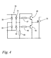
- the Fig. 4 shows an embodiment of the circuit for driving the FET 36.
- the rectifier 35 from the bridge circuit of the diodes 30 to 33 corresponds to that of Fig. 1 , A DC terminal of the rectifier 35 is connected to the source terminal of the FET 36 as well as in FIG Fig. 1 the case is.
- Fig. 4 is connected to the other DC terminal of the rectifier 35, the collector of a transistor 46, whose emitter is connected to the gate 4 of the FET 36.
- the base of the transistor 46 is connected via a resistor 47 to the DC terminal of the rectifier 35, to which also the collector of the transistor 46 is connected.
- Also connected to the gate of the FET 36 is the emitter of a transistor 48 whose collector is connected to the source of the FET.
- the base of the transistor 48 is connected via a resistor 49 to the DC power source, to which the base of the transistor 46 is located. Between the resistors 47, 49 and the connecting line from the rectifier 35 to the source terminal of the FET 36, a resistor 50 is connected.
- the transistor 46 is used to drive the FET 36, that is, at a corresponding output voltage at the rectifier 35, the base of the transistor 46 is driven so that it turns on and a current flows from the collector to the emitter and thus the gate of the FET 36 is driven.
- the transistor 46 is turned off and the base of the transistor 48 is driven so that it turns on and thus a current flows from the gate of the FET 36 to the connection line leading to the source connection. This way will the gate is shorted to the source terminal, thereby discharging the capacitance in the FET 36.
- the system is the same as that of Fig. 1 ,
- Control pulses up to 30 kHz can be transmitted. At the output no additional operating voltage is required, the transmitted energy is sufficient for the circuit of the FET 36 and thus the connection of the power switching terminals 38, 39 from. Due to the high clock frequency, the response time is very low.
- an inductive transformer 27 for example, a printed circuit board transformer is considered, so that the circuit is inexpensive overall. There are no aging or wear components used, so that a long life is given. The circuit is intended as a replacement for relays or optocouplers.
Landscapes
- Engineering & Computer Science (AREA)
- Power Engineering (AREA)
- Computer Networks & Wireless Communication (AREA)
- Signal Processing (AREA)
- Dc-Dc Converters (AREA)
- Electronic Switches (AREA)
- Power Conversion In General (AREA)
Abstract
Description
- Die Erfindung bezieht sich auf eine Schaltungsanordnung zur Übertragung von Signalen der im Oberbegriff des Anspruchs 1 angegebenen Gattung.
- Aus der
DE 32 10 509 A1 ist eine Schaltungsanordnung mit einer Koppeleinrichtung zur potenzialfreien Übertragung digitaler elektrischer Steuersignale bekannt. Diese Schaltungsanordnung umfasst Ansteuerklemmen, an denen Spannungssignale angelegt werden. Diese Spannungssignale werden in eine Impulsfolge umgesetzt, die einer Primärwicklung eines Ringkernübertragers zugeführt wird. Entsprechend dieser Impulsfolge wird in einer Sekundärwicklung des Ringkernübertragers eine Impulsfolge induziert, mit gleicher Spannung wie primärseitig. In einem an die Sekundärwicklung angeschlossenen Gleichrichter wird die Spannung gleichgerichtet und von dem Gleichrichter einem Gate eines Feldeffekttransistors (FET) zugeführt, der als Schalter zur Verbindung von Leistungsklemmen dient. - Der vorliegenden Erfindung liegt die Aufgabe zugrunde, eine Schaltungsanordnung der eingangs genannten Gattung zu schaffen, mit der Unabhängig von der Frequenz des Ansteuersignals eine Übertragung mit hoher Taktfrequenz und schneller Ansprechzeit erfolgt.
- Diese Aufgabe wird durch eine Schaltungsanordnung mit den Merkmalen des Anspruchs 1 gelöst.
- In Ausgestaltung der Erfindung kann das erste Gatter ein NAND-Gatter oder ein Schmitt-Trigger sein. Gemäß einer bevorzugten Weiterbildung des Grundgedankens der Erfindung ist vorgesehen, dass das Bauelement zur Invertierung des Signals aus einem weiteren invertierenden Gatter besteht. Durch die Invertierung des Signals ergibt sich eine von dem induktiven Übertrager übertragbare Spannung, die in dem nachgeschalteten Gleichrichter wieder in eine Gleichspannung umgeformt wird. Es ist weiter von Vorteil, dass an einem Ausgang des ersten Gatters die Eingänge eines zweiten Gatters angeschlossen sind und dessen Ausgang mit Eingängen des weiteren Gatters verbunden ist. Diese dem ersten Gatter folgenden Gatter dienen der Flankenversteilerung, wodurch sich ein exaktes Rechtecksignal ergibt.
- Vorzugsweise arbeitet die Schaltungsanordnung mit einer an den Ansteuerklemmen anliegenden Spannung, die im Bereich von 14 V bis 30 V liegt, wobei es sich um eine Gleichspannung oder ein digitales Signal mit einer Frequenz bis 30 kHz handeln kann. Der Spannungsregler ist so ausgelegt, dass er die Versorgungsspannung auf 14 V begrenzt. In weiterer Ausgestaltung der Schaltungsanordnung ist es zweckmäßig, dass das erste Gatter einen Schwingkreis darstellt, dessen Frequenz über die Kombination aus Widerstand und Kondensator definiert wird, wobei typischer Weise eine Frequenz von f = 1,7 MHz eingestellt wird. Das Hochfrequenzsignal hat durch die Hysterese im ersten Gatter annähernd die Form eines Rechtecksignals, das durch die weiteren Gatter zu einem exakten Rechtecksignal geformt wird.
- Es ist außerdem von Vorteil, eine Betriebsanzeige vorzusehen, die auf einfache Weise dadurch gestaltet sein kann, dass an einem Anschluss der Betriebsspannung eines der Gatter eine Leuchtdiode angeschlossen ist. Der Gleichrichter besteht vorzugsweise aus einer vier Dioden umfassenden Brückenschaltung, so dass eine Zweiweggleichrichtung erfolgt und somit beide Halbwellen gleichgerichtet werden. In einer Ausführungsform ist vorgesehen, dass eine Gleichstromklemme der Brückenschaltung direkt mit dem Gate des FET und die andere Gleichstromklemme mit dem Source-Anschluss des FET verbunden ist. Alternativ hierzu ist es auch möglich, dass zwischen einer Gleichstromklemme der Brückenschaltung und das Gate des FET ein Transistor geschaltet ist, über den das Gate ansteuerbar ist. Um die im FET vorhandene Kapazität zu entladen, kann zwischen dem Gate und dem Source-Anschluss des FET ein Widerstand angeschlossen oder ein Transistor vorgesehen sein. Außerdem ist es zweckmäßig, dass der Übertrager auf einer Platine als Leiterbahn ausgeführt ist und ein Ferritkern zur magnetischen Kopplung eingesetzt ist. Ausführungsbeispiele der Erfindung sind nachstehend anhand der Zeichnungen näher erläutert. In der Zeichnung zeigt:
- Fig. 1
- eine Schaltung zur Übertragung eines elektrischen Signals mittels induktiver Kopplung,
- Fig. 2
- ein Impulsdiagramm,
- Fig. 3
- ein Gatter mit Anschlüssen für die Betriebsspannung,
- Fig. 4
- eine Ausführungsvariante der Schaltung zur Ansteuerung des Feldeffekttransistors.
- Die Schaltung in
Fig. 1 weist Ansteuerklemmen 11 und 12 auf, an denen ein Schaltsignal angelegt werden kann, beispielsweise eine getaktete oder konstante Gleichspannung von 24 V. Zwischen die Ansteuerklemmen 11 und 12 ist ein Kondensator 13 geschaltet und parallel zu diesem eine Zener-Diode 14, wobei deren Katode mit der Ansteuerklemme 11 und deren Anode mit der Ansteuerklemme 12 verbunden sind. - Parallel zu dem Kondensator 13 und der Zener-Diode 14 ist ein Spannungsregler 15 geschaltet, der aus einem Transistor 16, einem Widerstand 17 und einer Zener-Diode 18 besteht. Dabei ist der Kollektor des Transistors 16 mit der Ansteuerklemme 11 und die Basis mit der Katode der Zener-Diode 18 verbunden, die anodenseitig mit der Ansteuerklemme 12 sowie einem Masseanschluss 20 verbunden ist. Der Widerstand 17 liegt zwischen dem Kollektor und der Basis des Transistors 16. Der Emitter ist mit einer Spannungsquelle 19 verbunden, die eine konstante Gleichspannung liefert. Der Spannungsregler 15 begrenzt die Eingangsspannung auf 14 V.
- Ein erstes invertierendes Gatter 21 ist im Ausführungsbeispiel als NAND-Gatter mit Funktion als Schmitt-Trigger ausgeführt und mit seinen Eingängen 1, 2 über einen Kondensator 22 mit der Anode der Zener-Diode 18 verbunden, und der Ausgang 3 ist über einen Widerstand 23 zur Rückkopplung mit dem invertierenden Eingang 1 des Gatters 21 verbunden. Das erste Gatter 21 stellt einen Schwingkreis dar, dessen Frequenz über die Kombination mit Widerstand 23 und Kondensator 22 definiert wird. Das erste Gatter 21 erzeugt somit durch die Hysterese ein am Ausgang 3 anstehendes, im Wesentlichen rechteckiges Signal. Das erste Gatter 21 mit der Rückführung des Ausgangssignals über den Widerstand 23 zu dem invertierenden Eingang und dem vorgeschalteten Kondensator 22 wirkt als astabilier Multivibrator und erzeugt ein Hochfrequenzsignal, das typischer Weise auf die Frequenz f = 1,7 MHz eingestellt wird. Das Signal am Ausgang 3 wird den Eingängen 5, 6 eines zweiten Gatters 24 zugeführt. Das zweite Gatter 24 ist im Ausführungsbeispiel ebenfalls ein NAND-Gatter mit Schmitt-Trigger Funktion , an dessen Ausgang 4 Eingänge 8, 9 eines dritten Gatters 25, ebenfalls ein NAND-Gatter oder Schmitt-Trigger, angeschlossen sind. Die beiden Gatter 24 und 25 dienen zur Flankenversteilerung des Rechtecksignals.
- Der Ausgang 10 des dritten Gatters 25 ist mit einer Primärwicklung 26 eines induktiven Übertragers 27 verbunden, deren anderes Ende unter Zwischenschaltung eines Widerstands 29 mit dem Ausgang 4 des zweiten Gatters 24 bzw. den Eingängen 8, 9 des dritten Gatters 25 verbunden ist. Am Ausgang 4 des zweiten Gatters und Ausgang 10 des dritten Gatters 25 liegt je ein invertiertes Rechtecksignal einer Frequenz f = 1,7 MHz an. Es ist somit eine rechteckige Wechselspannung, welche auf die Primärwicklung 26 des Übertragers 27 gegeben wird. Der induktive Übertrager 27 erzeugt in einer Sekundärwicklung 28 die gleiche Spannung, die an der Primärwicklung 26 anliegt. Die Primärwicklung 26 wird durch das Gatter 25 aktiv umgepolt und erhält somit immer die interne Versorgungsspannung. Dadurch wird die maximale Leistung im Übertrager 27 erzielt.
- Die Sekundärwicklung 28 ist mit einem aus vier Dioden 30, 31, 32 und 33 gebildeten Gleichrichter 35 verbunden, wobei zwischen einem Ende der Sekundärwicklung 28 und die Gleichrichterbrücke ein Widerstand 34 geschaltet ist. Im Gleichrichter 35 erfolgt eine Zweiweggleichrichtung, wodurch beide Halbwellen gleichgerichtet werden. Eine der Gleichstromklemmen des Gleichrichters 35 ist mit dem Source-Anschluss eines Feldeffekt-Transistors 36 verbunden und die andere Gleichstromklemme des Gleichrichters 35 ist an das Gate geschaltet. Die Welligkeit nach dem Brückengleichrichter wird durch die interne Kapazität des FET 36 ausreichend geglättet, so dass der FET 36 durchsteuert. Der Drain-Anschluss des FET 36 ist mit einer Leistungsschaltklemme 38 verbunden, an der eine positive Spannung anliegt. Die Kapazität des FET 36 glättet die von dem Gleichrichter abgegebene pulsierende Wechselspannung, wodurch der FET leitend wird. Zwischen das Gate und den Source-Anschluss des FET ist ein Widerstand 37 geschaltet, der dazu dient, die im FET 36 enthaltene Kapazität zu entladen.
- An den Source-Anschluss des FET 36 ist auch eine Leistungsklemme 39 geschaltet, an die ein Verbraucher angeschlossen ist. An die Leistungsklemmen 38 ist eine Katode einer Zener-Diode 40 angeschlossen, deren Anode mit der Leistungsklemme 39 verbunden ist.
- Bei Anliegen einer Versorgungsspannung Ui an den Ansteuerklemmen 11, 12 arbeitet der induktive Übertrager zum Schalten eines Verbrauchers an eine Spannungsquelle. Die Versorgungsspannung. Ui hat vorzugsweise eine Nennspannung von 24 V, das System arbeitet jedoch im Bereich von Ui = 14 V bis 30 V. Ui kann eine Gleichspannung oder eine pulsierende Gleichspannung bis 30 kHz sein. Die Versorgungsspannung ist gleichzeitig Taktgenerierungsspannung. Die Versorgungsspannung wird im Spannungsregler 15 auf eine konstante Spannung von 14 V heruntergeregelt, die für die Gatter 21, 24, 25 erforderlich ist. Bei steigender Versorgungsspannung Ui schwingt der Oszillator an, so dass ein Signal übertragen wird.
- Im ersten Gatter 21 mit Kombination von Widerstand 23 und Kondensator 22 wird das Hochfrequenzsignal von f = 1,7 MHz erzeugt, das annähernd die Form eines Rechtecksignals hat. Die nachgeschalteten Gatter 24, 25 dienen zur Flankenversteilerung und durch Invertieren des Signals im dritten Gatter 25 wird an die Primärwicklung 26 des Übertragers 27 eine Wechselspannung geliefert, wobei induktiv in der Sekundärwicklung 28 die gleiche Spannung mit der Frequenz f = 1,7 MHz erzeugt wird. Diese Wechselspannung wird in dem nachgeschalteten Gleichrichter 35 gleichgerichtet, wobei durch die Zweiweggleichrichtung als Signal eine unmittelbare Folge positiver Halbwellen entsteht. Dieses Signal dient zur Ansteuerung des FET 36, der die Verbindung zwischen den Leistungsschaltklemmen 38 und 39 schließt. Der FET 36 benötigt keine Hilfsspannung, die übertragene Energie reicht für die Funktion aus.
- Liegt an den Ansteuerklemmen 11, 12 keine Spannung Ui an, so arbeitet die gesamte Schaltung nicht. Somit wird auch kein Strom verbraucht.
- In
Fig. 2 ist ein Impulsdiagramm gezeigt, in dem zwei Steuerimpulse dargestellt sind, wobei als Beispiel die Frequenz fs = 30 kHz beträgt. Während des Steuerimpulses erzeugt das erste Gatter, das als astabiler Multivibrator wirkt, das zuFig. 1 beschriebene Hochfrequenzsignal von f = 1,7 MHz. - In
Fig. 3 ist ein Gatter, beispielsweise das erste Gatter 21 mit Anschlüssen 41, 42 für die Betriebsspannung des Gatters dargestellt. Der Anschluss 41 ist mit der Katode einer Leuchtdiode 43 verbunden, die anodenseitig an eine Spannungsquelle 44 geschaltet ist. Der Anschluss 42 ist mit einem Masseanschluss 45 verbunden. Die Leuchtdiode 43 wird beim Betrieb des Gatters 21 vom Strom durchflossen und dient damit als Betriebsanzeige des inFig. 1 gezeigten Systems. - Die
Fig. 4 zeigt eine Ausführungsvariante der Schaltung zur Ansteuerung des FET 36. Der Gleichrichter 35 aus der Brückenschaltung der Dioden 30 bis 33 entspricht demjenigen derFig. 1 . Eine Gleichstromklemme des Gleichrichters 35 ist mit dem Source-Anschluss des FET 36 verbunden, wie dies ebenso inFig. 1 der Fall ist. InFig. 4 ist an die andere Gleichstromklemme des Gleichrichters 35 der Kollektor eines Transistors 46 geschaltet, dessen Emitter mit dem Gate 4 des FET 36 verbunden ist. Die Basis des Transistors 46 ist über einen Widerstand 47 mit der Gleichstromklemme des Gleichrichters 35 verbunden, an die auch der Kollektor des Transistors 46 geschaltet ist. Mit dem Gate des FET 36 ist auch der Emitter eines Transistors 48 verbunden, dessen Kollektor mit dem Source-Anschluss des FET verbunden ist. Die Basis des Transistors 48 ist über einen Widerstand 49 an die Gleichstromquelle geschaltet, an der auch die Basis des Transistors 46 liegt. Zwischen den Widerständen 47, 49 und der Verbindungsleitung vom Gleichrichter 35 zum Source-Anschluss des FET 36 ist ein Widerstand 50 geschaltet. Der Transistor 46 dient zur Ansteuerung des FET 36, das heißt, bei einer entsprechenden Ausgangsspannung am Gleichrichter 35 wird die Basis des Transistors 46 angesteuert, so dass dieser durchschaltet und ein Strom vom Kollektor zum Emitter fließt und damit das Gate des FET 36 angesteuert wird. Sobald am Gleichrichter 35 die Ausgangsspannung einen vorgegebenen Wert unterschreitet, sperrt der Transistor 46 und die Basis des Transistors 48 wird angesteuert, so dass dieser durchschaltet und somit ein Strom vom Gate des FET 36 zu der zum Source-Anschluss führenden Verbindungsleitung fließt. Auf diese Weise wird das Gate mit dem Source-Anschluss kurzgeschlossen, wodurch ein Entladen der Kapazität im FET 36 erfolgt. Im Übrigen ist das System gleich demjenigen derFig. 1 . - Mit der vorstehend beschriebenen Schaltung zu
Fig. 1 bzw. der Ausführungsvariante gemäßFig. 4 können Steuerimpulse bis zu 30 kHz übertragen werden. Am Ausgang ist keine zusätzliche Betriebsspannung erforderlich, die übertragene Energie reicht zur Schaltung des FET 36 und damit zur Verbindung der Leistungsschaltklemmen 38, 39 aus. Durch die hohe Taktfrequenz ist die Ansprechzeit sehr gering. Als induktiver Übertrager 27 kommt beispielsweise ein Leiterplattentrafo in Betracht, so dass die Schaltung insgesamt kostengünstig ist. Es sind keine alternden oder verschleißenden Bauteile eingesetzt, so dass eine lange Lebensdauer gegeben ist. Die Schaltung ist als Ersatz für Relais oder Optokoppler vorgesehen.
Claims (16)
- Schaltungsanordnung zur Übertragung von Signalen, wobei Ansteuerklemmen (11, 12) zum Anlegen einer Spannung (Ui) und eine nachgeordnete Baugruppe zur Erzeugung einer Impulsfolge vorgesehen sind, wobei diese Baugruppe ausgangsseitig an eine Primärwicklung (26) eines induktiven Übertragers (27) angeschlossen und eine Sekundärwicklung (28) des Übertragers (27) mit einem Gleichrichter (35) verbunden ist, an dem ausgangsseitig ein Gate eines FET (36) angeschlossen ist und der FET (36) als Schalter zwischen Leistungsschaltklemmen (38, 39) dient,
dadurch gekennzeichnet, dass mit den Ansteuerklemmen (11, 12) ein Spannungsregler (15) verbunden ist und die Baugruppe zur Erzeugung der Impulsfolge ein mit einer Rückkopplung versehenes erstes invertierendes Gatter (21) und ein weiteres Bauelement zur Invertierung des Signals umfasst, wobei das invertierende Gatter (21) eingangsseitig über einen Kondensator (22) mit dem Spannungsregler (15) verbunden ist. - Schaltungsanordnung nach Anspruch 1,
dadurch gekennzeichnet, dass das invertierende Gatter (21) ein NAND-Gatter oder ein Schmitt-Trigger ist. - Schaltungsanordnung nach Anspruch 1 oder 2,
dadurch gekennzeichnet, dass das weitere Bauelement zur Invertierung des Signals aus einem weiteren Gatter (25) besteht. - Schaltungsanordnung nach Anspruch 3,
dadurch gekennzeichnet, dass an einem Ausgang (3) des ersten Gatters (21) die Eingänge (5, 6) eines zweiten Gatters (24) angeschlossen sind und dessen Ausgang (4) mit Eingängen (8, 9) des weiteren Gatters (25) verbunden ist. - Schaltungsanordnung nach einem der Ansprüche 1 bis 4,
dadurch gekennzeichnet, dass die an den Ansteuerklemmen (11, 12) anliegende Spannung (Ui) in einem Bereich von 14 V bis 30 V liegt. - Schaltungsanordnung nach Anspruch 5,
dadurch gekennzeichnet, dass die Spannung (Ui) ein digitales Signal mit einer maximalen Frequenz fs = 30 kHz ist. - Schaltungsanordnung nach einem der Ansprüche 1 bis 6,
dadurch gekennzeichnet, dass der Spannungsregler (15) die interne Versorgungsspannung auf 14 V begrenzt. - Schaltungsanordnung nach einem der Ansprüche 1 bis 7,
dadurch gekennzeichnet, dass das erste Gatter (21) einen Schwingkreis darstellt, dessen Frequenz über die Kombination mit Widerstand (23) und Kondensator (22) definiert wird, wobei typischer Weise eine Frequenz von f = 1,7 MHz eingestellt wird. - Schaltungsanordnung nach einem der Ansprüche 1 bis 8,
dadurch gekennzeichnet, dass an der Betriebsspannung des Gatters (21, 24, 25) eine Leuchtdiode (43) zur Anzeige der Eingangsspannung (Ui) angeschlossen ist. - Schaltungsanordnung nach einem der Ansprüche 1 bis 9,
dadurch gekennzeichnet, dass der Gleichrichter (15) eine aus vier Dioden (30, 31, 32, 33) gebildete Brückenschaltung ist. - Schaltungsanordnung nach Anspruch 10,
dadurch gekennzeichnet, dass eine Gleichstromklemme der Brückenschaltung direkt mit dem Gate des FET (36) und die andere Gleichstromklemme mit dem Source-Anschluss des FET (36) verbunden ist. - Schaltungsanordnung nach Anspruch 10,
dadurch gekennzeichnet, dass zwischen einer Gleichstromklemme der Brückenschaltung und das Gate des FET (36) ein Transistor (46) geschaltet ist, über den das Gate ansteuerbar ist. - Schaltungsanordnung nach Anspruch 10,
dadurch gekennzeichnet, dass zwischen dem Gate und dem Source-Anschluss des FET (36) ein Widerstand angeschlossen ist. - Schaltungsanordnung nach Anspruch 10,
dadurch gekennzeichnet, dass zwischen dem Gate und dem Source-Anschluss des FET (36) ein Transistor (48) vorgesehen ist. - Schaltungsanordnung nach einem der Ansprüche 3 bis 14,
dadurch gekennzeichnet, dass die Primärwicklung (26) durch das Gatter (25) aktiv umgepolt wird und somit immer die gesamte interne Versorgungsspannung erhält, wodurch die maximale Leistung in dem Übertrager (27) erzielt wird. - Schaltungsanordnung nach einem der Ansprüche 1 bis 15,
dadurch gekennzeichnet, dass der Übertrager (27) auf einer Platine als Leiterbahn ausgeführt ist und ein Ferritkern zur magnetischen Kopplung eingesetzt ist.
Priority Applications (1)
| Application Number | Priority Date | Filing Date | Title |
|---|---|---|---|
| EP10016003.5A EP2469782B1 (de) | 2010-12-23 | 2010-12-23 | Schaltunfsanordnung zur Übertragung von Signalen |
Applications Claiming Priority (1)
| Application Number | Priority Date | Filing Date | Title |
|---|---|---|---|
| EP10016003.5A EP2469782B1 (de) | 2010-12-23 | 2010-12-23 | Schaltunfsanordnung zur Übertragung von Signalen |
Publications (2)
| Publication Number | Publication Date |
|---|---|
| EP2469782A1 true EP2469782A1 (de) | 2012-06-27 |
| EP2469782B1 EP2469782B1 (de) | 2021-03-31 |
Family
ID=44062672
Family Applications (1)
| Application Number | Title | Priority Date | Filing Date |
|---|---|---|---|
| EP10016003.5A Active EP2469782B1 (de) | 2010-12-23 | 2010-12-23 | Schaltunfsanordnung zur Übertragung von Signalen |
Country Status (1)
| Country | Link |
|---|---|
| EP (1) | EP2469782B1 (de) |
Citations (5)
| Publication number | Priority date | Publication date | Assignee | Title |
|---|---|---|---|---|
| WO1981000658A1 (en) * | 1979-08-31 | 1981-03-05 | Electro Med Eng Pty Ltd | Telephone line data isolator |
| DE3210509A1 (de) | 1982-03-23 | 1982-12-09 | Gerd Dr.-Ing. 3167 Burgdorf Harms | Schnelle elektronische koppeleinrichtung zur potentialfreien uebertragung digitaler elektrischer steuersignale |
| US4425663A (en) * | 1980-06-13 | 1984-01-10 | Tcl, Inc. | Low input capacitance data network transceiver |
| US20050036604A1 (en) * | 1997-04-22 | 2005-02-17 | Silicon Laboratories Inc. | Direct digital access arrangement circuitry and method for connecting DSL circuitry to phone lines |
| US20080069249A1 (en) * | 2006-09-14 | 2008-03-20 | Stmicroelectronics S.A. | Transfer of digital data through a transformer |
-
2010
- 2010-12-23 EP EP10016003.5A patent/EP2469782B1/de active Active
Patent Citations (5)
| Publication number | Priority date | Publication date | Assignee | Title |
|---|---|---|---|---|
| WO1981000658A1 (en) * | 1979-08-31 | 1981-03-05 | Electro Med Eng Pty Ltd | Telephone line data isolator |
| US4425663A (en) * | 1980-06-13 | 1984-01-10 | Tcl, Inc. | Low input capacitance data network transceiver |
| DE3210509A1 (de) | 1982-03-23 | 1982-12-09 | Gerd Dr.-Ing. 3167 Burgdorf Harms | Schnelle elektronische koppeleinrichtung zur potentialfreien uebertragung digitaler elektrischer steuersignale |
| US20050036604A1 (en) * | 1997-04-22 | 2005-02-17 | Silicon Laboratories Inc. | Direct digital access arrangement circuitry and method for connecting DSL circuitry to phone lines |
| US20080069249A1 (en) * | 2006-09-14 | 2008-03-20 | Stmicroelectronics S.A. | Transfer of digital data through a transformer |
Also Published As
| Publication number | Publication date |
|---|---|
| EP2469782B1 (de) | 2021-03-31 |
Similar Documents
| Publication | Publication Date | Title |
|---|---|---|
| DE2756799C2 (de) | Fremdgetakteter, tastverhältnisgeregelter Gleichspannungswandler | |
| DE69412984T2 (de) | Schaltregler | |
| DE2345073A1 (de) | Netzgeraet | |
| EP2262078A1 (de) | Anordnung und Verfahren zur induktiven Energieübertragung | |
| EP1148623A2 (de) | Stromversorgungseinrichtung | |
| EP2206213B1 (de) | Galvansiche trennung zwischen zell-ladungsausgleich und steuerung eines hybridantriebs | |
| DE102019005176A1 (de) | Buck-boost-wandler sowie verfahren und treiber zu deren steuerung | |
| DE4238388C2 (de) | Elektronische Schaltungsanordnung zur Ansteuerung einer UV-Strahlungsquelle | |
| DE2434574C3 (de) | Zündanordnung für Brennkraftmaschinen | |
| DE102015014638B4 (de) | Schaltungsvorrichtung und Verfahren zur kontaktlosen Energie- und Datenübertragung | |
| EP2138015A1 (de) | Schaltungsanordnung zum betreiben mindestens einer entladungslampe und verfahren zum erzeugen einer hilfsspannung | |
| DE3610156C2 (de) | ||
| EP3021126A1 (de) | Verfahren und Vorrichtung zur potentialgetrennten Strommessung | |
| EP2469782B1 (de) | Schaltunfsanordnung zur Übertragung von Signalen | |
| DE102012007451B4 (de) | Wandler für ein Leuchtmittel, LED- Konverter und Verfahren zum Betreiben eines LLC-Resonanzwandlers | |
| EP2151067B1 (de) | Induktive übertragungsvorrichtung für elektrische energie und daten | |
| EP1701434A2 (de) | Ansteuerschaltung für den Schalter in einem Schatznetzteil | |
| EP0509343A2 (de) | Verfahren zum Betreiben eines Schaltreglers sowie Anordnung | |
| DE3701805A1 (de) | Schaltungsanordnung zur stromversorgung von niederspannungsverbrauchern | |
| DE102014223377B4 (de) | Betriebsschaltung zur Versorgung eines Leuchtmittels, LED-Konverter, System und Verfahren zum Betreiben einer Betriebsschaltung | |
| EP3100591B1 (de) | Erfassung eines led-moduls | |
| EP0232915B1 (de) | Schaltungsanordnung einer auf Resonanz basierenden Gleichspannungsquelle | |
| EP3552458B1 (de) | Schaltungsanordnung und verfahren zum betreiben eines leuchtmittels | |
| WO1998043266A1 (de) | Elektromagnetischer stellantrieb | |
| DE849431C (de) | Schaltung zur Erzeugung einer Gleichspannung, insbesondere zur Speisung von Elektronenstrahlroehren |
Legal Events
| Date | Code | Title | Description |
|---|---|---|---|
| 17P | Request for examination filed |
Effective date: 20120125 |
|
| AK | Designated contracting states |
Kind code of ref document: A1 Designated state(s): AL AT BE BG CH CY CZ DE DK EE ES FI FR GB GR HR HU IE IS IT LI LT LU LV MC MK MT NL NO PL PT RO RS SE SI SK SM TR |
|
| AX | Request for extension of the european patent |
Extension state: BA ME |
|
| PUAI | Public reference made under article 153(3) epc to a published international application that has entered the european phase |
Free format text: ORIGINAL CODE: 0009012 |
|
| RIC1 | Information provided on ipc code assigned before grant |
Ipc: H04L 25/02 20060101ALI20121031BHEP Ipc: H03K 3/00 20060101AFI20121031BHEP |
|
| 17Q | First examination report despatched |
Effective date: 20130320 |
|
| APBK | Appeal reference recorded |
Free format text: ORIGINAL CODE: EPIDOSNREFNE |
|
| APBN | Date of receipt of notice of appeal recorded |
Free format text: ORIGINAL CODE: EPIDOSNNOA2E |
|
| APBR | Date of receipt of statement of grounds of appeal recorded |
Free format text: ORIGINAL CODE: EPIDOSNNOA3E |
|
| APAF | Appeal reference modified |
Free format text: ORIGINAL CODE: EPIDOSCREFNE |
|
| APBX | Invitation to file observations in appeal sent |
Free format text: ORIGINAL CODE: EPIDOSNOBA2E |
|
| APBZ | Receipt of observations in appeal recorded |
Free format text: ORIGINAL CODE: EPIDOSNOBA4E |
|
| APBT | Appeal procedure closed |
Free format text: ORIGINAL CODE: EPIDOSNNOA9E |
|
| REG | Reference to a national code |
Ref country code: DE Ref legal event code: R079 Ref document number: 502010016881 Country of ref document: DE Free format text: PREVIOUS MAIN CLASS: H04L0025020000 Ipc: H03K0017691000 |
|
| GRAP | Despatch of communication of intention to grant a patent |
Free format text: ORIGINAL CODE: EPIDOSNIGR1 |
|
| STAA | Information on the status of an ep patent application or granted ep patent |
Free format text: STATUS: GRANT OF PATENT IS INTENDED |
|
| RIC1 | Information provided on ipc code assigned before grant |
Ipc: H03K 17/691 20060101AFI20200717BHEP Ipc: H04L 25/02 20060101ALI20200717BHEP |
|
| GRAJ | Information related to disapproval of communication of intention to grant by the applicant or resumption of examination proceedings by the epo deleted |
Free format text: ORIGINAL CODE: EPIDOSDIGR1 |
|
| STAA | Information on the status of an ep patent application or granted ep patent |
Free format text: STATUS: EXAMINATION IS IN PROGRESS |
|
| INTG | Intention to grant announced |
Effective date: 20200818 |
|
| INTC | Intention to grant announced (deleted) | ||
| GRAP | Despatch of communication of intention to grant a patent |
Free format text: ORIGINAL CODE: EPIDOSNIGR1 |
|
| STAA | Information on the status of an ep patent application or granted ep patent |
Free format text: STATUS: GRANT OF PATENT IS INTENDED |
|
| INTG | Intention to grant announced |
Effective date: 20201028 |
|
| GRAS | Grant fee paid |
Free format text: ORIGINAL CODE: EPIDOSNIGR3 |
|
| GRAA | (expected) grant |
Free format text: ORIGINAL CODE: 0009210 |
|
| STAA | Information on the status of an ep patent application or granted ep patent |
Free format text: STATUS: THE PATENT HAS BEEN GRANTED |
|
| AK | Designated contracting states |
Kind code of ref document: B1 Designated state(s): AL AT BE BG CH CY CZ DE DK EE ES FI FR GB GR HR HU IE IS IT LI LT LU LV MC MK MT NL NO PL PT RO RS SE SI SK SM TR |
|
| REG | Reference to a national code |
Ref country code: GB Ref legal event code: FG4D Free format text: NOT ENGLISH Ref country code: CH Ref legal event code: EP |
|
| REG | Reference to a national code |
Ref country code: AT Ref legal event code: REF Ref document number: 1378101 Country of ref document: AT Kind code of ref document: T Effective date: 20210415 Ref country code: DE Ref legal event code: R096 Ref document number: 502010016881 Country of ref document: DE |
|
| REG | Reference to a national code |
Ref country code: IE Ref legal event code: FG4D Free format text: LANGUAGE OF EP DOCUMENT: GERMAN |
|
| REG | Reference to a national code |
Ref country code: LT Ref legal event code: MG9D |
|
| PG25 | Lapsed in a contracting state [announced via postgrant information from national office to epo] |
Ref country code: NO Free format text: LAPSE BECAUSE OF FAILURE TO SUBMIT A TRANSLATION OF THE DESCRIPTION OR TO PAY THE FEE WITHIN THE PRESCRIBED TIME-LIMIT Effective date: 20210630 Ref country code: BG Free format text: LAPSE BECAUSE OF FAILURE TO SUBMIT A TRANSLATION OF THE DESCRIPTION OR TO PAY THE FEE WITHIN THE PRESCRIBED TIME-LIMIT Effective date: 20210630 Ref country code: FI Free format text: LAPSE BECAUSE OF FAILURE TO SUBMIT A TRANSLATION OF THE DESCRIPTION OR TO PAY THE FEE WITHIN THE PRESCRIBED TIME-LIMIT Effective date: 20210331 Ref country code: HR Free format text: LAPSE BECAUSE OF FAILURE TO SUBMIT A TRANSLATION OF THE DESCRIPTION OR TO PAY THE FEE WITHIN THE PRESCRIBED TIME-LIMIT Effective date: 20210331 |
|
| PG25 | Lapsed in a contracting state [announced via postgrant information from national office to epo] |
Ref country code: SE Free format text: LAPSE BECAUSE OF FAILURE TO SUBMIT A TRANSLATION OF THE DESCRIPTION OR TO PAY THE FEE WITHIN THE PRESCRIBED TIME-LIMIT Effective date: 20210331 Ref country code: LV Free format text: LAPSE BECAUSE OF FAILURE TO SUBMIT A TRANSLATION OF THE DESCRIPTION OR TO PAY THE FEE WITHIN THE PRESCRIBED TIME-LIMIT Effective date: 20210331 Ref country code: RS Free format text: LAPSE BECAUSE OF FAILURE TO SUBMIT A TRANSLATION OF THE DESCRIPTION OR TO PAY THE FEE WITHIN THE PRESCRIBED TIME-LIMIT Effective date: 20210331 |
|
| REG | Reference to a national code |
Ref country code: NL Ref legal event code: MP Effective date: 20210331 |
|
| PG25 | Lapsed in a contracting state [announced via postgrant information from national office to epo] |
Ref country code: SM Free format text: LAPSE BECAUSE OF FAILURE TO SUBMIT A TRANSLATION OF THE DESCRIPTION OR TO PAY THE FEE WITHIN THE PRESCRIBED TIME-LIMIT Effective date: 20210331 Ref country code: LT Free format text: LAPSE BECAUSE OF FAILURE TO SUBMIT A TRANSLATION OF THE DESCRIPTION OR TO PAY THE FEE WITHIN THE PRESCRIBED TIME-LIMIT Effective date: 20210331 Ref country code: NL Free format text: LAPSE BECAUSE OF FAILURE TO SUBMIT A TRANSLATION OF THE DESCRIPTION OR TO PAY THE FEE WITHIN THE PRESCRIBED TIME-LIMIT Effective date: 20210331 Ref country code: CZ Free format text: LAPSE BECAUSE OF FAILURE TO SUBMIT A TRANSLATION OF THE DESCRIPTION OR TO PAY THE FEE WITHIN THE PRESCRIBED TIME-LIMIT Effective date: 20210331 Ref country code: EE Free format text: LAPSE BECAUSE OF FAILURE TO SUBMIT A TRANSLATION OF THE DESCRIPTION OR TO PAY THE FEE WITHIN THE PRESCRIBED TIME-LIMIT Effective date: 20210331 |
|
| PG25 | Lapsed in a contracting state [announced via postgrant information from national office to epo] |
Ref country code: RO Free format text: LAPSE BECAUSE OF FAILURE TO SUBMIT A TRANSLATION OF THE DESCRIPTION OR TO PAY THE FEE WITHIN THE PRESCRIBED TIME-LIMIT Effective date: 20210331 Ref country code: IS Free format text: LAPSE BECAUSE OF FAILURE TO SUBMIT A TRANSLATION OF THE DESCRIPTION OR TO PAY THE FEE WITHIN THE PRESCRIBED TIME-LIMIT Effective date: 20210731 Ref country code: ES Free format text: LAPSE BECAUSE OF FAILURE TO SUBMIT A TRANSLATION OF THE DESCRIPTION OR TO PAY THE FEE WITHIN THE PRESCRIBED TIME-LIMIT Effective date: 20210331 Ref country code: SK Free format text: LAPSE BECAUSE OF FAILURE TO SUBMIT A TRANSLATION OF THE DESCRIPTION OR TO PAY THE FEE WITHIN THE PRESCRIBED TIME-LIMIT Effective date: 20210331 Ref country code: PL Free format text: LAPSE BECAUSE OF FAILURE TO SUBMIT A TRANSLATION OF THE DESCRIPTION OR TO PAY THE FEE WITHIN THE PRESCRIBED TIME-LIMIT Effective date: 20210331 Ref country code: PT Free format text: LAPSE BECAUSE OF FAILURE TO SUBMIT A TRANSLATION OF THE DESCRIPTION OR TO PAY THE FEE WITHIN THE PRESCRIBED TIME-LIMIT Effective date: 20210802 |
|
| REG | Reference to a national code |
Ref country code: DE Ref legal event code: R097 Ref document number: 502010016881 Country of ref document: DE |
|
| PG25 | Lapsed in a contracting state [announced via postgrant information from national office to epo] |
Ref country code: DK Free format text: LAPSE BECAUSE OF FAILURE TO SUBMIT A TRANSLATION OF THE DESCRIPTION OR TO PAY THE FEE WITHIN THE PRESCRIBED TIME-LIMIT Effective date: 20210331 Ref country code: AL Free format text: LAPSE BECAUSE OF FAILURE TO SUBMIT A TRANSLATION OF THE DESCRIPTION OR TO PAY THE FEE WITHIN THE PRESCRIBED TIME-LIMIT Effective date: 20210331 |
|
| PGFP | Annual fee paid to national office [announced via postgrant information from national office to epo] |
Ref country code: GB Payment date: 20211222 Year of fee payment: 12 Ref country code: FR Payment date: 20211224 Year of fee payment: 12 |
|
| PLBE | No opposition filed within time limit |
Free format text: ORIGINAL CODE: 0009261 |
|
| STAA | Information on the status of an ep patent application or granted ep patent |
Free format text: STATUS: NO OPPOSITION FILED WITHIN TIME LIMIT |
|
| PGFP | Annual fee paid to national office [announced via postgrant information from national office to epo] |
Ref country code: CH Payment date: 20211221 Year of fee payment: 12 |
|
| 26N | No opposition filed |
Effective date: 20220104 |
|
| PG25 | Lapsed in a contracting state [announced via postgrant information from national office to epo] |
Ref country code: IS Free format text: LAPSE BECAUSE OF FAILURE TO SUBMIT A TRANSLATION OF THE DESCRIPTION OR TO PAY THE FEE WITHIN THE PRESCRIBED TIME-LIMIT Effective date: 20210731 |
|
| PGFP | Annual fee paid to national office [announced via postgrant information from national office to epo] |
Ref country code: IT Payment date: 20211224 Year of fee payment: 12 |
|
| PG25 | Lapsed in a contracting state [announced via postgrant information from national office to epo] |
Ref country code: MC Free format text: LAPSE BECAUSE OF FAILURE TO SUBMIT A TRANSLATION OF THE DESCRIPTION OR TO PAY THE FEE WITHIN THE PRESCRIBED TIME-LIMIT Effective date: 20210331 |
|
| REG | Reference to a national code |
Ref country code: BE Ref legal event code: MM Effective date: 20211231 |
|
| PG25 | Lapsed in a contracting state [announced via postgrant information from national office to epo] |
Ref country code: LU Free format text: LAPSE BECAUSE OF NON-PAYMENT OF DUE FEES Effective date: 20211223 Ref country code: IE Free format text: LAPSE BECAUSE OF NON-PAYMENT OF DUE FEES Effective date: 20211223 |
|
| PG25 | Lapsed in a contracting state [announced via postgrant information from national office to epo] |
Ref country code: BE Free format text: LAPSE BECAUSE OF NON-PAYMENT OF DUE FEES Effective date: 20211231 |
|
| REG | Reference to a national code |
Ref country code: AT Ref legal event code: MM01 Ref document number: 1378101 Country of ref document: AT Kind code of ref document: T Effective date: 20211223 |
|
| PG25 | Lapsed in a contracting state [announced via postgrant information from national office to epo] |
Ref country code: AT Free format text: LAPSE BECAUSE OF NON-PAYMENT OF DUE FEES Effective date: 20211223 |
|
| PG25 | Lapsed in a contracting state [announced via postgrant information from national office to epo] |
Ref country code: HU Free format text: LAPSE BECAUSE OF FAILURE TO SUBMIT A TRANSLATION OF THE DESCRIPTION OR TO PAY THE FEE WITHIN THE PRESCRIBED TIME-LIMIT; INVALID AB INITIO Effective date: 20101223 Ref country code: CY Free format text: LAPSE BECAUSE OF FAILURE TO SUBMIT A TRANSLATION OF THE DESCRIPTION OR TO PAY THE FEE WITHIN THE PRESCRIBED TIME-LIMIT Effective date: 20210331 |
|
| PG25 | Lapsed in a contracting state [announced via postgrant information from national office to epo] |
Ref country code: GR Free format text: LAPSE BECAUSE OF FAILURE TO SUBMIT A TRANSLATION OF THE DESCRIPTION OR TO PAY THE FEE WITHIN THE PRESCRIBED TIME-LIMIT Effective date: 20210331 |
|
| REG | Reference to a national code |
Ref country code: CH Ref legal event code: PL |
|
| GBPC | Gb: european patent ceased through non-payment of renewal fee |
Effective date: 20221223 |
|
| PG25 | Lapsed in a contracting state [announced via postgrant information from national office to epo] |
Ref country code: LI Free format text: LAPSE BECAUSE OF NON-PAYMENT OF DUE FEES Effective date: 20221231 Ref country code: GB Free format text: LAPSE BECAUSE OF NON-PAYMENT OF DUE FEES Effective date: 20221223 Ref country code: CH Free format text: LAPSE BECAUSE OF NON-PAYMENT OF DUE FEES Effective date: 20221231 |
|
| PG25 | Lapsed in a contracting state [announced via postgrant information from national office to epo] |
Ref country code: FR Free format text: LAPSE BECAUSE OF NON-PAYMENT OF DUE FEES Effective date: 20221231 |
|
| PG25 | Lapsed in a contracting state [announced via postgrant information from national office to epo] |
Ref country code: IT Free format text: LAPSE BECAUSE OF NON-PAYMENT OF DUE FEES Effective date: 20221223 |
|
| PGFP | Annual fee paid to national office [announced via postgrant information from national office to epo] |
Ref country code: DE Payment date: 20231214 Year of fee payment: 14 |
|
| PG25 | Lapsed in a contracting state [announced via postgrant information from national office to epo] |
Ref country code: MK Free format text: LAPSE BECAUSE OF FAILURE TO SUBMIT A TRANSLATION OF THE DESCRIPTION OR TO PAY THE FEE WITHIN THE PRESCRIBED TIME-LIMIT Effective date: 20210331 |
|
| PG25 | Lapsed in a contracting state [announced via postgrant information from national office to epo] |
Ref country code: MT Free format text: LAPSE BECAUSE OF FAILURE TO SUBMIT A TRANSLATION OF THE DESCRIPTION OR TO PAY THE FEE WITHIN THE PRESCRIBED TIME-LIMIT Effective date: 20210331 |
|
| REG | Reference to a national code |
Ref country code: DE Ref legal event code: R119 Ref document number: 502010016881 Country of ref document: DE |
|
| PG25 | Lapsed in a contracting state [announced via postgrant information from national office to epo] |
Ref country code: DE Free format text: LAPSE BECAUSE OF NON-PAYMENT OF DUE FEES Effective date: 20250701 |
|
| PG25 | Lapsed in a contracting state [announced via postgrant information from national office to epo] |
Ref country code: TR Free format text: LAPSE BECAUSE OF FAILURE TO SUBMIT A TRANSLATION OF THE DESCRIPTION OR TO PAY THE FEE WITHIN THE PRESCRIBED TIME-LIMIT Effective date: 20210331 |