EP2469740B1 - Methods and receiver for positioning of clock related spurious signals - Google Patents
Methods and receiver for positioning of clock related spurious signals Download PDFInfo
- Publication number
- EP2469740B1 EP2469740B1 EP10196540.8A EP10196540A EP2469740B1 EP 2469740 B1 EP2469740 B1 EP 2469740B1 EP 10196540 A EP10196540 A EP 10196540A EP 2469740 B1 EP2469740 B1 EP 2469740B1
- Authority
- EP
- European Patent Office
- Prior art keywords
- frequency
- signal
- carrier
- oscillator
- sub
- Prior art date
- Legal status (The legal status is an assumption and is not a legal conclusion. Google has not performed a legal analysis and makes no representation as to the accuracy of the status listed.)
- Active
Links
Images


Classifications
-
- H—ELECTRICITY
- H04—ELECTRIC COMMUNICATION TECHNIQUE
- H04L—TRANSMISSION OF DIGITAL INFORMATION, e.g. TELEGRAPHIC COMMUNICATION
- H04L27/00—Modulated-carrier systems
- H04L27/26—Systems using multi-frequency codes
- H04L27/2601—Multicarrier modulation systems
- H04L27/2647—Arrangements specific to the receiver only
- H04L27/2649—Demodulators
-
- H—ELECTRICITY
- H04—ELECTRIC COMMUNICATION TECHNIQUE
- H04B—TRANSMISSION
- H04B15/00—Suppression or limitation of noise or interference
- H04B15/02—Reducing interference from electric apparatus by means located at or near the interfering apparatus
- H04B15/04—Reducing interference from electric apparatus by means located at or near the interfering apparatus the interference being caused by substantially sinusoidal oscillations, e.g. in a receiver or in a tape-recorder
- H04B15/06—Reducing interference from electric apparatus by means located at or near the interfering apparatus the interference being caused by substantially sinusoidal oscillations, e.g. in a receiver or in a tape-recorder by local oscillators of receivers
-
- H—ELECTRICITY
- H04—ELECTRIC COMMUNICATION TECHNIQUE
- H04L—TRANSMISSION OF DIGITAL INFORMATION, e.g. TELEGRAPHIC COMMUNICATION
- H04L27/00—Modulated-carrier systems
- H04L27/26—Systems using multi-frequency codes
- H04L27/2601—Multicarrier modulation systems
- H04L27/2647—Arrangements specific to the receiver only
- H04L27/2655—Synchronisation arrangements
- H04L27/2657—Carrier synchronisation
-
- H—ELECTRICITY
- H04—ELECTRIC COMMUNICATION TECHNIQUE
- H04L—TRANSMISSION OF DIGITAL INFORMATION, e.g. TELEGRAPHIC COMMUNICATION
- H04L27/00—Modulated-carrier systems
- H04L27/0014—Carrier regulation
- H04L2027/0016—Stabilisation of local oscillators
-
- H—ELECTRICITY
- H04—ELECTRIC COMMUNICATION TECHNIQUE
- H04L—TRANSMISSION OF DIGITAL INFORMATION, e.g. TELEGRAPHIC COMMUNICATION
- H04L27/00—Modulated-carrier systems
- H04L27/0014—Carrier regulation
- H04L2027/0024—Carrier regulation at the receiver end
- H04L2027/0026—Correction of carrier offset
- H04L2027/0032—Correction of carrier offset at baseband and passband
-
- H—ELECTRICITY
- H04—ELECTRIC COMMUNICATION TECHNIQUE
- H04L—TRANSMISSION OF DIGITAL INFORMATION, e.g. TELEGRAPHIC COMMUNICATION
- H04L27/00—Modulated-carrier systems
- H04L27/0014—Carrier regulation
- H04L2027/0044—Control loops for carrier regulation
- H04L2027/0063—Elements of loops
- H04L2027/0065—Frequency error detectors
Definitions
- This invention pertains in general to the field of suppression of clock spurious signals. More particularly the invention relates to methods and a receiver for positioning of clock spurious signals for decreasing the negative effect of said spurious signals on an Orthogonal Frequency Division Multiplexing (OFDM) signal received by a receiver.
- OFDM Orthogonal Frequency Division Multiplexing
- Interference in a mobile terminal can be created by internal components or units.
- One typical example of internally generated interference is the interference caused by a clock signal leaking into the Radio Frequency (RF) parts of the transceiver unit.
- the harmonics of the clock signal extend into the RF domain and might therefore interfere with the received signal. This is especially a problem at low power levels of the received signal.
- Sensitivity is a key parameter for receivers due to the fact that the sensitivity level is related to the coverage for a mobile terminal. Hence, from an operator point of view, there is a selling argument for mobile terminals or modems having a good sensitivity.
- This solution however, has a drawback in that it requires a sampling rate in the order of 10 MHz of the received signal in combination with the need for a plurality of filter taps for establishing a sufficiently narrow notch filter, since the leakage signal is typically only about 100 - 1000 Hz wide.
- Such a filter is typically very expensive in terms of size, cost, and power or current consumption.
- WO 2009/093156 A1 was cited in the European Search Report to represent technological background art.
- WO 2009/093156 A1 concerns a method and an apparatus to cancel additive sinusoidal disturbances in OFDM receivers.
- a method and an apparatus are contemplated for cancelling additive sinusoidal disturbances of a known frequency in OFDM receivers which arise e.g. from clock signals that are present for frequency reference, mixer control, and A/D converter control, as well as harmonics and mixing products of those periodic signals, coupling into some point in the receiver chain and appearing as rotating complex exponentials superimposed to complex baseband receive signals.
- an estimation of an amplitude and phase of a disturbing superimposed tone with a known frequency is obtained and the amplitude and phase estimation is used to cancel the spurious tone preventing a degradation of receiver sensitivity while achieving low implementation complexity.
- the present invention seeks to mitigate, alleviate or eliminate one or more of the above-identified deficiencies in the prior art and disadvantages singly or in any combination and solves at least the above mentioned problem by providing a method and an arrangement according to the appended patent claims.
- the general solution is to position the clock harmonics spurious signal relative to sub-carriers of a received OFDM signal, such that the negative effect of the spurious signal is reduced.
- a method in a receiver of positioning a spurious signal for reducing the impact of the spurious signal on a received OFDM signal comprises determining the frequency of a spurious signal based on a frequency of a first oscillator.
- the frequency for the respective sub-carrier of the OFDM signal and the difference between the frequency of a sub-carrier and the frequency of a spurious signal are also determined.
- at least one of: the frequency of the first oscillator and a parameter related to the frequency of a second oscillator are adjusted, to decrease the frequency difference between the sub-carrier and the spurious signal.
- the parameter related to the frequency of the second oscillator of the method may further comprise a control parameter for the frequency of the second oscillator.
- the step of adjusting the control parameter for the frequency of the second oscillator may be performed such that the frequency of the second oscillator equals the carrier frequency of the OFDM signal plus the determined difference between the frequency of the spurious signal and the frequency of the subcarrier.
- the method may further comprise applying a digital de-rotator to shift the OFDM signal with a frequency amount corresponding to the difference between the frequency of the spurious signal and the frequency of a sub-carrier.
- the method may further comprise removing a Direct Current, DC component from a base band signal, prior to setting the frequency of the digital de-rotator.
- Adjusting the frequency of the first, oscillator, according to the method, may be performed prior to determining the frequency of the spurious signal.
- Adjusting the control parameter related to the frequency of a second oscillator may be performed such that the frequency of the second oscillator is equal to the carrier frequency of the OFDM signal.
- the method may further comprise suppression of a spurious signal by setting soft values of the sub-carriers affected by any one of previous steps to zero, or by estimation of a spurious signal and subtraction of said spurious signal.
- the sub-carrier in the step of adjusting the control parameter, within the method may comprise the sub-carrier closest to the spurious signal.
- a receiver for positioning a spurious signal for reducing the impact of the spurious signal on a received OFDM signal comprises a down-converting mixer configured to determine the frequency of the spurious signal based on a frequency of a first oscillator, and to determine the frequency for the respective sub-carrier of the OFDM signal and determining the difference between the frequency of a sub-carrier and a spurious signal.
- the receiver also comprises a controller operatively connected to the down-converting mixer, wherein the controller is configured to adjust at least one of: the frequency of the first oscillator and a parameter related to the frequency of a second oscillator, to decrease the frequency difference between the sub-carrier and the spurious signal.
- a mobile terminal or a receiver utilizes the knowledge of the frequency of potential signals that may leak in to the pass-band of a received signal.
- the potential signals are often harmonics of internal clock signals.
- a basic idea of the embodiments of the present invention is to adapt an internally generated carrier frequency such that a spurious signal is positioned at, or at least near, a sub-carrier frequency.
- the present invention comprises a few embodiments of which two will be briefly sketched already at this stage.
- adaptation of the frequency of both the internally generated clock signal as well a parameter in the Phase Locked Loop, PLL transforming the frequency of a clock signal to a Local Oscillator, LO carrier frequency is performed.
- the spurious signal originating from the clock signal is translated to a frequency corresponding to a sub-carrier frequency.
- adaptation is performed of either an internally generated clock signal or the LO carrier frequency by at maximum half the sub-carrier spacing at radio frequency and a digital frequency compensator that is introduced to compensate for a LO offset.
- suppression of spurious signals is performed in a subsequent base band processing, for instance, by either setting soft values on the affected sub-carrier to zero (so called nulling), or by estimation and subsequent subtraction of spurious signals. It shall be mentioned that suppression is not limited by the two mentioned methods. Rather other methods may just as well be applied.
- a signal having a frequency F is distributed over different frequency bins, when transformed by a Fast Fourier Transform, FFT of a certain dimension. The closer F is to a certain carrier frequency, the fewer sub-carriers are affected.
- performance degradation is much smaller when the frequency of a spurious signal is close to a sub-carrier frequency, as compared with the case where the frequency of the spurious signal is approximately in the middle of two adjacent sub-carriers.
- the idea of the embodiments of the present invention is to utilize the knowledge of the spurious frequency and to position the spurious signal accordingly, to only affect one, or a small number of, stib-carrier(s).
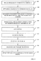
- Figure 1 illustrates a signal flow diagram related to a general embodiment of the present invention.
- a receiver or a mobile terminal determines the frequency of a spurious signal in step 102. This determination is based on the frequency of a first oscillator. The mobile terminal or receiver then determines the frequency of the respective OFDM sub-carrier and the frequency difference between a sub-carrier and a spurious signal, in step 104. Thereafter, a parameter is adjusted to decrease the frequency difference between a spurious signal and a sub ⁇ carrier in step 106.
- Figure 2 illustrates a flow chart of method steps according to one embodiment of the invention.
- Figure 3 presenting a block diagram related to said embodiment of the present invention.
- reducing the impact of the spurious signal on a received OFDM signal comprises obtaining the carrier frequency Fc of the OFDM signal, in step 202. Thereafter, the frequency of the relevant spurious signal is determined, in step 204.
- the relevant spurious signals are those which might interfere with the received OFDM signal. This determination is based on settings of a crystal oscillator, XO.
- the spurious signal is typically a harmonic of the frequency of the crystal oscillator, Fxo.
- the frequency of a sub-carrier that is closest to a spurious signal is determined in step 206.
- step 208 the clock frequency Fxo is set to the down-scaled frequency of the closest sub-carrier. Having performed that, it is determined a Phase Locked Loop, PLL parameter or factor with which a frequency of a local oscillator Flo equals the frequency of the carrier Fc, in step 210. In the subsequent step of 212, the determined PLL factor from step 210 is now used whereby Flo is set to Fc.
- PLL Phase Locked Loop
- an offset for the frequency Fxo of the XO and the PLL factor or parameter are determined.
- the PLL transforms the Fxo frequency up to the carrier frequency Fc.
- the offset is determined such that the frequency of the LO, Flo, matches the carrier frequency, Fc. Having determined the offset and the PLL parameter, the Fxo and the PLL parameter or factor are then retuned.
- the adaptation of Fxo and the PLL factor to achieve that Flo equals to Fc can be made for all signal levels. It may alternatively be made based on the received signal level, or more precisely at low signal levels, since the problem with interfering spurious signals mainly exists at low signal levels close to the reference sensitivity level, approximately below -90 dBm.
- the received OFDM signal is then digitalized by an Analog to Digital Converter, ADC converting the analog OFDM signal, in step 214. Having a digital signal, a Fast Fourier Transform, FFT is applied in step 216.
- ADC Analog to Digital Converter
- step 218 the resulting signal is detected and compensating means for suppression of the spurious signal is applied.
- Examples of such base band processing are setting the soft values on the affected sub-carriers to zero, or estimation and subsequent subtraction of the spurious signals. It must be emphasized that suppression is not limited by the two mentioned examples. Rather, other methods may just as well be applied.
- FIG 3 presents a block diagram related to the embodiment of Figure 2 of the present invention. It is implicitly illustrated that the OFDM signal is received by a front-end transceiving unit RX 302 including a down-converting mixer.
- the frequency Flo of a Local Oscillator, LO 304 is based on the frequency Fxo of the Crystal Oscillator, 306.
- a Control Unit, CU 308 controls the LO frequency Flo, using a Phase Locked Loop, PLL.
- the down-converted OFDM signal is Low-Pass filtered in 310, obtaining a base-band of the OFDM signal.
- the signal is thereafter digitalized by an Analog to
- ADC Analog Converter
- FFT 3114 a Fast Fourier Transform
- detector 316 the spurious signal is then suppressed by processing of the FFT signal.
- the front-end transceiving unit 302 supplies a baseband signal of the OFDM signal to the detector 316 that demodulates the received signal.
- the potential spurious frequency that might interfere with the received signal is determined. As mentioned above this derivation is based on the current settings of the X-tal Oscillator, XO.
- the spurious signal is typically a harmonic of the XO frequency Fxo. Once the frequency of the spurious signal is determined, the frequency difference between the spurious signal and the closest sub-carrier may be determined, which difference is less than or equal to the sub-carrier spacing.
- the spurious signal it is determined that translating the spurious signal to an adjacent sub-carrier might have a large effect on the performance in case this sub-carrier contains specifically important information and therefore the spurious signal is instead translated slightly further in frequency. For example, sub-carriers assigned for reference signals or pilots could be avoided not to interfere with channel estimation etc. For this reason, the spurious signal may accordingly be translated to a neighboring, but not adjacent, sub-carrier frequency.
- the XO has a frequency Fxo 26.001 MHz, and the carrier frequency used is 2600 MHz, with a system bandwidth 5 MHz. It is noted that the division ratio in the PLL is 99.996154, which is 2600 divided by 26.001 MHz.
- the closest sub-carrier is thus 5 kHz away from the spurious signal.
- Figure 4 presents a flow chart of method steps of another method for reducing the impact of spurious signal on a received OFDM signal.
- step 402 comprises obtaining the carrier frequency of the received OFDM frequency
- step 404 comprises determining the frequency of a spurious signal, Fs.
- step 406 the frequency difference AF between the spurious signal and the closest sub-carrier is determined.
- step 408 the frequency Flo of the Local Oscillator, LO, is offset from the frequency of the carrier Fc by the determined frequency difference AF. This step may involve adjusting a PLL parameter to achieve that Flo Fc + ⁇ F.
- step 410 comprises digitalizing the down-converted OFDM signal by performing an Analog to Digital Conversion, ADC.
- a High-Pass Direct Current, DC notch filter may be passed in step 412, to eliminate any DC content of the resulting received OFDM signal. It can be mentioned that this HP filtering in step 412 can alternatively be performed on the analog signal prior to the ADC in step 410.
- step 414 the resulting OFDM signal is now digitally rotated back or derotated by ⁇ F, (or digitally rotated with -AF). In this step, all frequencies are thus turned to their correct values, after having been offset an amount AF too far in step 408.
- Steps 416 and 418 correspond to steps 216 and 218 of Figure 2 , and thus comprise performing discrete Fast Fourier Transform, FFT, and detecting signals and compensating for spurious signals, respectively, as mentioned above.
- the OFDM signal is received by a front-end transceiving unit RX 502 including a down-converting mixer.
- the frequency Flo of a Local Oscillator, LO 504 is based on the frequency Fxo of the X-tal Oscillator, XO 506.
- a Control Unit, CU 508 controls the LO frequency Flo, using a Phase Locked Loop, PLL.
- the down-converted OFDM signal is Low-Pass filtered in 510, obtaining a base-band signal of the OFDM signal.
- the signal is thereafter digitalized by an Analog to Digital Converter, ADC, 512 after which the digital signal may be subjected to High-Pass filter 514.
- ADC Analog to Digital Converter
- this filter is also a Direct Current notch filter, removing any DC component of the OFDM signal.
- step 516 all frequencies of the OFDM signal are corrected by an amount corresponding to an earlier determined offset, AF, being the difference between the spurious signal and, the closest or a close, sub-carrier.
- step 518 FFT is performed and signals are detected in the detector 520, wherein suppression of spurious signals is performed.
- the front-end transceiving unit 502 supplies a baseband signal of the OFDM signal to the detector that demodulates the received signal.
- the potential spurious signals or frequencies that might interfere with the current received carrier frequency is determined. This derivation is based on the current settings and frequency Fxo of the crystal oscillator, XO 506. As mentioned above, the spurious signal or frequency is typically a harmonic of the Fxo frequency.
- the frequency difference between the spurious signal and a close or the closest sub-carrier is determined. This difference is less than or equal to half the sub-carrier spacing of 15 kHz, in the case of the closest sub-carrier.
- the Flo frequency is first offset with that frequency difference, after which the offset is digitally compensated by a digital de-rotator, placed after the ADC 512 but prior to the FFT 518.
- a digital de-rotator placed after the ADC 512 but prior to the FFT 518.
- an embodiment may also comprise a DC notch filter 514 prior to the digital frequency de-rotator 516.
- a DC offset of varying magnitude is generated in the down-converting mixer 502 and in baseband blocks due to imperfections, and in order to not introduce DC leakage in the FFT, a time domain notch filter, removing the DC may be introduced.
- the DC notch is preferably introduced in the digital domain as illustrated in Figure 5 , but may alternatively be introduced as an analog filter prior to the ADC 512.
- the spurious signal may instead be positioned only at nearby sub-carriers allocated for a specific need such that the impact of the spurious signal will have the least impact.
- sub-carriers assigned for reference signals or pilots could be avoided not to interfere with channel estimation etc.
- embodiments of the invention also comprise the concept of translating the spurious signals to a neighboring, but not an adjacent, sub-carrier.
- adjusting of the frequency may be performed by the first oscillator, as well as of a parameter related to the frequency of a second oscillator, to decrease the frequency difference between a sub-carrier and a spurious signal.
- Figure 6 schematically presents an arrangement of positioning a spurious signal for reducing the impact of the spurious signal on a received OFDM signal by down-converting said OFDM signal to a base band.
- the arrangement 600 comprises a down-converting mixer 602 that is configured to determine the frequency of the spurious signal based on a frequency of a first oscillator.
- the down-converting mixer is further configured to determine the frequency for the respective sub-carrier of the OFDM signal and determine the difference between the frequency of a sub-carrier and a spurious signal.
- the arrangement 600 also comprises a controller 604 that is operatively connected to the down-converting mixer 602, wherein the controller is configured to adjust at least one of: the frequency of the first oscillator and a parameter related to the frequency of a second oscillator, to decrease the frequency difference between a subcarrier and a spurious signal.
Description
- This invention pertains in general to the field of suppression of clock spurious signals. More particularly the invention relates to methods and a receiver for positioning of clock spurious signals for decreasing the negative effect of said spurious signals on an Orthogonal Frequency Division Multiplexing (OFDM) signal received by a receiver.
- Interference in a mobile terminal can be created by internal components or units. The smaller the mobile terminal or a transceiver unit is, the larger is the risk for internally generated interference. One typical example of internally generated interference is the interference caused by a clock signal leaking into the Radio Frequency (RF) parts of the transceiver unit. The harmonics of the clock signal extend into the RF domain and might therefore interfere with the received signal. This is especially a problem at low power levels of the received signal.
- Sensitivity is a key parameter for receivers due to the fact that the sensitivity level is related to the coverage for a mobile terminal. Hence, from an operator point of view, there is a selling argument for mobile terminals or modems having a good sensitivity.
- The problem with spurious signals in the receiver band, originated from a baseband clock signal, to mention one example, is typically mitigated by proper layout design of different blocks in the baseband and in the radio chip as well as on higher level routing of these blocks. However, based on practical experience such signal leakage can hardly be completely removed by layout design only. There can hence remain some residual leakage causing interference.
- One solution of this problem according to prior art is to introduce a narrow-band notch filter in the time domain for filtering out the spurious signal. Since the clock frequency and the frequency of potential harmonics are known, narrow-band or notch filters might be introduced into the receiver chain.
- This solution, however, has a drawback in that it requires a sampling rate in the order of 10 MHz of the received signal in combination with the need for a plurality of filter taps for establishing a sufficiently narrow notch filter, since the leakage signal is typically only about 100 - 1000 Hz wide. Such a filter is typically very expensive in terms of size, cost, and power or current consumption.
- Therefore, there is a need for methods and arrangements improving the receiver performance close to the reference sensitivity level in the case of having harmonics from the baseband clock leaking into the receiver chain that do not require costly notch filters that consume considerable power.
-
WO 2009/093156 A1 was cited in the European Search Report to represent technological background art.WO 2009/093156 A1 concerns a method and an apparatus to cancel additive sinusoidal disturbances in OFDM receivers. In this document, a method and an apparatus are contemplated for cancelling additive sinusoidal disturbances of a known frequency in OFDM receivers which arise e.g. from clock signals that are present for frequency reference, mixer control, and A/D converter control, as well as harmonics and mixing products of those periodic signals, coupling into some point in the receiver chain and appearing as rotating complex exponentials superimposed to complex baseband receive signals. According to the method and apparatus an estimation of an amplitude and phase of a disturbing superimposed tone with a known frequency is obtained and the amplitude and phase estimation is used to cancel the spurious tone preventing a degradation of receiver sensitivity while achieving low implementation complexity. - The present invention seeks to mitigate, alleviate or eliminate one or more of the above-identified deficiencies in the prior art and disadvantages singly or in any combination and solves at least the above mentioned problem by providing a method and an arrangement according to the appended patent claims.
- The general solution is to position the clock harmonics spurious signal relative to sub-carriers of a received OFDM signal, such that the negative effect of the spurious signal is reduced.
- According to one aspect of the present invention, a method in a receiver of positioning a spurious signal for reducing the impact of the spurious signal on a received OFDM signal, is disclosed. The method comprises determining the frequency of a spurious signal based on a frequency of a first oscillator. The frequency for the respective sub-carrier of the OFDM signal and the difference between the frequency of a sub-carrier and the frequency of a spurious signal are also determined. Moreover, at least one of: the frequency of the first oscillator and a parameter related to the frequency of a second oscillator are adjusted, to decrease the frequency difference between the sub-carrier and the spurious signal.
- The parameter related to the frequency of the second oscillator of the method, may further comprise a control parameter for the frequency of the second oscillator.
- The step of adjusting the control parameter for the frequency of the second oscillator, according to the method, may be performed such that the frequency of the second oscillator equals the carrier frequency of the OFDM signal plus the determined difference between the frequency of the spurious signal and the frequency of the subcarrier.
- The method may further comprise applying a digital de-rotator to shift the OFDM signal with a frequency amount corresponding to the difference between the frequency of the spurious signal and the frequency of a sub-carrier.
- The method may further comprise removing a Direct Current, DC component from a base band signal, prior to setting the frequency of the digital de-rotator.
- Adjusting the frequency of the first, oscillator, according to the method, may be performed prior to determining the frequency of the spurious signal.
- Adjusting the control parameter related to the frequency of a second oscillator, according to the method, may be performed such that the frequency of the second oscillator is equal to the carrier frequency of the OFDM signal.
- The method may further comprise suppression of a spurious signal by setting soft values of the sub-carriers affected by any one of previous steps to zero, or by estimation of a spurious signal and subtraction of said spurious signal.
- The sub-carrier in the step of adjusting the control parameter, within the method, may comprise the sub-carrier closest to the spurious signal.
- According to a second aspect of the present invention, a receiver for positioning a spurious signal for reducing the impact of the spurious signal on a received OFDM signal, is disclosed. The receiver comprises a down-converting mixer configured to determine the frequency of the spurious signal based on a frequency of a first oscillator, and to determine the frequency for the respective sub-carrier of the OFDM signal and determining the difference between the frequency of a sub-carrier and a spurious signal. The receiver also comprises a controller operatively connected to the down-converting mixer, wherein the controller is configured to adjust at least one of: the frequency of the first oscillator and a parameter related to the frequency of a second oscillator, to decrease the frequency difference between the sub-carrier and the spurious signal.
- Embodiments of the present invention come with the following advantages:
- With the proposed invention the resulting spurious signal is placed in the vicinity of, or directly on a sub-carrier frequency which reduces the negative performance impact of the spurious signal, and thereby improves the sensitivity of the receiver.
- These and other aspects, features and advantages of which the invention is capable of will be apparent and elucidated from the following description of embodiments of the present invention, reference being made to the accompanying drawings, in which
-
Figs. 1 ,2 and4 schematically illustrate a signal flow diagram related to embodiments of the present invention; -
Figs. 3 and 5 schematically present block diagrams related to embodiments of the present invention; and -
Fig. 6 schematically illustrates a block diagram of an arrangement according to the present invention. -
- DC
- Direct Current
- FFT
- Fast Fourier Transform
- LO
- Local Oscillator
- OFDM
- Orthogonal Frequency Division Multiplexing
- PLL
- Phase-Locked Loop
- XO
- Crystal Oscillator or X-tal Oscillator
- Within the present invention, a mobile terminal or a receiver utilizes the knowledge of the frequency of potential signals that may leak in to the pass-band of a received signal. The potential signals are often harmonics of internal clock signals.
- A basic idea of the embodiments of the present invention is to adapt an internally generated carrier frequency such that a spurious signal is positioned at, or at least near, a sub-carrier frequency. The present invention comprises a few embodiments of which two will be briefly sketched already at this stage.
- Within a first embodiment, adaptation of the frequency of both the internally generated clock signal as well a parameter in the Phase Locked Loop, PLL transforming the frequency of a clock signal to a Local Oscillator, LO carrier frequency, is performed. In this embodiment, the spurious signal originating from the clock signal is translated to a frequency corresponding to a sub-carrier frequency.
- Within a second embodiment of the present invention, adaptation is performed of either an internally generated clock signal or the LO carrier frequency by at maximum half the sub-carrier spacing at radio frequency and a digital frequency compensator that is introduced to compensate for a LO offset.
- Within the two mentioned embodiments suppression of spurious signals is performed in a subsequent base band processing, for instance, by either setting soft values on the affected sub-carrier to zero (so called nulling), or by estimation and subsequent subtraction of spurious signals. It shall be mentioned that suppression is not limited by the two mentioned methods. Rather other methods may just as well be applied.
- It can also be mentioned that a signal having a frequency F is distributed over different frequency bins, when transformed by a Fast Fourier Transform, FFT of a certain dimension. The closer F is to a certain carrier frequency, the fewer sub-carriers are affected.
- Thus, performance degradation is much smaller when the frequency of a spurious signal is close to a sub-carrier frequency, as compared with the case where the frequency of the spurious signal is approximately in the middle of two adjacent sub-carriers.
- Hence, the idea of the embodiments of the present invention is to utilize the knowledge of the spurious frequency and to position the spurious signal accordingly, to only affect one, or a small number of, stib-carrier(s).
- Embodiments of the present invention will now be described.
-
Figure 1 illustrates a signal flow diagram related to a general embodiment of the present invention. - According to one embodiment, a receiver or a mobile terminal determines the frequency of a spurious signal in
step 102. This determination is based on the frequency of a first oscillator. The mobile terminal or receiver then determines the frequency of the respective OFDM sub-carrier and the frequency difference between a sub-carrier and a spurious signal, instep 104. Thereafter, a parameter is adjusted to decrease the frequency difference between a spurious signal and a sub~carrier instep 106. -
Figure 2 illustrates a flow chart of method steps according to one embodiment of the invention. Reference will also be made toFigure 3 presenting a block diagram related to said embodiment of the present invention. - According to this embodiment, reducing the impact of the spurious signal on a received OFDM signal comprises obtaining the carrier frequency Fc of the OFDM signal, in
step 202. Thereafter, the frequency of the relevant spurious signal is determined, instep 204. The relevant spurious signals are those which might interfere with the received OFDM signal. This determination is based on settings of a crystal oscillator, XO. The spurious signal is typically a harmonic of the frequency of the crystal oscillator, Fxo. Then, the frequency of a sub-carrier that is closest to a spurious signal, is determined instep 206. - In the subsequent step,
step 208, the clock frequency Fxo is set to the down-scaled frequency of the closest sub-carrier. Having performed that, it is determined a Phase Locked Loop, PLL parameter or factor with which a frequency of a local oscillator Flo equals the frequency of the carrier Fc, instep 210. In the subsequent step of 212, the determined PLL factor fromstep 210 is now used whereby Flo is set to Fc. - In other words, an offset for the frequency Fxo of the XO and the PLL factor or parameter are determined. The PLL transforms the Fxo frequency up to the carrier frequency Fc. The offset is determined such that the frequency of the LO, Flo, matches the carrier frequency, Fc. Having determined the offset and the PLL parameter, the Fxo and the PLL parameter or factor are then retuned.
- The adaptation of Fxo and the PLL factor to achieve that Flo equals to Fc, can be made for all signal levels. It may alternatively be made based on the received signal level, or more precisely at low signal levels, since the problem with interfering spurious signals mainly exists at low signal levels close to the reference sensitivity level, approximately below -90 dBm.
- Having set both the frequency of the local oscillator by using the PLL factor, the received OFDM signal is then digitalized by an Analog to Digital Converter, ADC converting the analog OFDM signal, in
step 214. Having a digital signal, a Fast Fourier Transform, FFT is applied instep 216. - In
step 218, the resulting signal is detected and compensating means for suppression of the spurious signal is applied. Examples of such base band processing are setting the soft values on the affected sub-carriers to zero, or estimation and subsequent subtraction of the spurious signals. It must be emphasized that suppression is not limited by the two mentioned examples. Rather, other methods may just as well be applied. -
Figure 3 presents a block diagram related to the embodiment ofFigure 2 of the present invention. It is implicitly illustrated that the OFDM signal is received by a front-endtransceiving unit RX 302 including a down-converting mixer. The frequency Flo of a Local Oscillator,LO 304 is based on the frequency Fxo of the Crystal Oscillator, 306. A Control Unit,CU 308 controls the LO frequency Flo, using a Phase Locked Loop, PLL. - The down-converted OFDM signal is Low-Pass filtered in 310, obtaining a base-band of the OFDM signal. The signal is thereafter digitalized by an Analog to
- Digital Converter, ADC, after which the digital signal is subjected to a Fast Fourier Transform,
FFT 314. In adetector 316 the spurious signal is then suppressed by processing of the FFT signal. - The front-
end transceiving unit 302 supplies a baseband signal of the OFDM signal to thedetector 316 that demodulates the received signal. - Based on the current received carrier frequency of the OFDM signal, the potential spurious frequency that might interfere with the received signal is determined. As mentioned above this derivation is based on the current settings of the X-tal Oscillator, XO. The spurious signal is typically a harmonic of the XO frequency Fxo. Once the frequency of the spurious signal is determined, the frequency difference between the spurious signal and the closest sub-carrier may be determined, which difference is less than or equal to the sub-carrier spacing.
- According to an alternative embodiment, it is determined that translating the spurious signal to an adjacent sub-carrier might have a large effect on the performance in case this sub-carrier contains specifically important information and therefore the spurious signal is instead translated slightly further in frequency. For example, sub-carriers assigned for reference signals or pilots could be avoided not to interfere with channel estimation etc. For this reason, the spurious signal may accordingly be translated to a neighboring, but not adjacent, sub-carrier frequency.
- In the following an example is presented showing how to set the frequency of the LO and the XO, as well as how to set the PLL factor or parameter.
- Assume that the XO has a frequency Fxo 26.001 MHz, and the carrier frequency used is 2600 MHz, with a system bandwidth 5 MHz. It is noted that the division ratio in the PLL is 99.996154, which is 2600 divided by 26.001 MHz.
- Further, the 100th harmonics of the Fxo is then @ f=2600.1 MHz, which is within the system bandwidth, BW, of 2597.5 MHz to 2602.5 MHz. The sub-carrier closest to the spurious signal is @ f=2600.105 MHz, being 2600.100 MHz + N x 15 kHz, where N = 7. The closest sub-carrier is thus 5 kHz away from the spurious signal. By setting the Fxo to the down-scaled frequency of the closest sub-carrier 26.00105 MHz and the PLL parameter or division ratio to 99.9959617, being 2600 divided by 26.00105, the carrier frequency is kept @ 2600 MHz and the spurious signal is @ a sub-carrier frequency, namely 2600.105 MHz.
- By achieving such a close matching, only one sub-carrier will be affected by the spurious signal, so that the impact can be effectively mitigated by simple coding.
- Some receiver architectures do not allow adaptation of Fxo frequency of the XO. For such cases, an alternative embodiment of the present invention is presented.
- For this reason
Figure 4 presents a flow chart of method steps of another method for reducing the impact of spurious signal on a received OFDM signal. - The first two steps in
Figure 4 are the same as those presented inFigure 2 , for a different embodiment of the present invention. It is nevertheless briefly mentioned thatstep 402 comprises obtaining the carrier frequency of the received OFDM frequency, and thatstep 404 comprises determining the frequency of a spurious signal, Fs. - In
step 406 the frequency difference AF between the spurious signal and the closest sub-carrier is determined. Instep 408, the frequency Flo of the Local Oscillator, LO, is offset from the frequency of the carrier Fc by the determined frequency difference AF. This step may involve adjusting a PLL parameter to achieve that Flo Fc + ΔF. - Thereafter,
step 410 comprises digitalizing the down-converted OFDM signal by performing an Analog to Digital Conversion, ADC. A High-Pass Direct Current, DC notch filter may be passed instep 412, to eliminate any DC content of the resulting received OFDM signal. It can be mentioned that this HP filtering instep 412 can alternatively be performed on the analog signal prior to the ADC instep 410. - It can be mentioned means other than the ones mentioned above, can be used to reducing DC contents of the resulting OFDM signal.
- In
step 414, the resulting OFDM signal is now digitally rotated back or derotated by ΔF, (or digitally rotated with -AF). In this step, all frequencies are thus turned to their correct values, after having been offset an amount AF too far instep 408. -
Steps steps Figure 2 , and thus comprise performing discrete Fast Fourier Transform, FFT, and detecting signals and compensating for spurious signals, respectively, as mentioned above. - With reference to
Figure 5 presenting a block diagram related to the embodiment ofFigure 4 of the present invention. It is implicitly illustrated that the OFDM signal is received by a front-endtransceiving unit RX 502 including a down-converting mixer. The frequency Flo of a Local Oscillator,LO 504 is based on the frequency Fxo of the X-tal Oscillator,XO 506. A Control Unit,CU 508 controls the LO frequency Flo, using a Phase Locked Loop, PLL. - The down-converted OFDM signal is Low-Pass filtered in 510, obtaining a base-band signal of the OFDM signal. The signal is thereafter digitalized by an Analog to Digital Converter, ADC, 512 after which the digital signal may be subjected to High-
Pass filter 514. As mentioned above, this filter is also a Direct Current notch filter, removing any DC component of the OFDM signal. - Now, in
step 516, all frequencies of the OFDM signal are corrected by an amount corresponding to an earlier determined offset, AF, being the difference between the spurious signal and, the closest or a close, sub-carrier. Instep 518 FFT is performed and signals are detected in thedetector 520, wherein suppression of spurious signals is performed. - Thus, the front-
end transceiving unit 502 supplies a baseband signal of the OFDM signal to the detector that demodulates the received signal. - That is, the potential spurious signals or frequencies that might interfere with the current received carrier frequency is determined. This derivation is based on the current settings and frequency Fxo of the crystal oscillator,
XO 506. As mentioned above, the spurious signal or frequency is typically a harmonic of the Fxo frequency. - Once the frequency of the spurious frequency is determined, the frequency difference between the spurious signal and a close or the closest sub-carrier is determined. This difference is less than or equal to half the sub-carrier spacing of 15 kHz, in the case of the closest sub-carrier. The Flo frequency is first offset with that frequency difference, after which the offset is digitally compensated by a digital de-rotator, placed after the
ADC 512 but prior to theFFT 518. As presented above, an embodiment may also comprise aDC notch filter 514 prior to thedigital frequency de-rotator 516. - A DC offset of varying magnitude is generated in the down-converting
mixer 502 and in baseband blocks due to imperfections, and in order to not introduce DC leakage in the FFT, a time domain notch filter, removing the DC may be introduced. The DC notch is preferably introduced in the digital domain as illustrated inFigure 5 , but may alternatively be introduced as an analog filter prior to theADC 512. - As an alternative to positioning the spurious signal at the nearest sub-carrier frequency, it may instead be positioned only at nearby sub-carriers allocated for a specific need such that the impact of the spurious signal will have the least impact. For example, sub-carriers assigned for reference signals or pilots could be avoided not to interfere with channel estimation etc. Hence embodiments of the invention also comprise the concept of translating the spurious signals to a neighboring, but not an adjacent, sub-carrier.
- According to an alternative embodiment of the present invention, adjusting of the frequency may be performed by the first oscillator, as well as of a parameter related to the frequency of a second oscillator, to decrease the frequency difference between a sub-carrier and a spurious signal.
-
Figure 6 schematically presents an arrangement of positioning a spurious signal for reducing the impact of the spurious signal on a received OFDM signal by down-converting said OFDM signal to a base band. Thearrangement 600 comprises a down-convertingmixer 602 that is configured to determine the frequency of the spurious signal based on a frequency of a first oscillator. The down-converting mixer is further configured to determine the frequency for the respective sub-carrier of the OFDM signal and determine the difference between the frequency of a sub-carrier and a spurious signal. Thearrangement 600 also comprises acontroller 604 that is operatively connected to the down-convertingmixer 602, wherein the controller is configured to adjust at least one of: the frequency of the first oscillator and a parameter related to the frequency of a second oscillator, to decrease the frequency difference between a subcarrier and a spurious signal. - It must be emphasized that the present invention can be varied in many ways.
- The presented embodiments of the present invention are only a few examples of the variety of embodiments that are comprised within the present invention.
- The embodiments of the present invention provide at least the following advantages:
- With the proposed invention the resulting spurious frequency is positioned at least close a sub-carrier frequency which reduces the performance impact of the spurious signal, and thereby improves the receiver performance.
- Although the present invention has been described above with reference to specific embodiments, it is not intended to be limited to the specific form set forth herein. Rather, the invention is limited only by the accompanying claims and other embodiments than the specific above are equally possible within the scope of these appended claims.
- In the claims, the term "comprises/comprising" does not exclude the presence of other elements or steps. Furthermore, although individually listed, a plurality of means, or method steps may be implemented by e.g. a single unit or processor. Additionally, although individual features may be included in different claims, these may possibly advantageously be combined, and the inclusion in different claims does not imply that a combination of features is not feasible and/or advantageous. In addition, singular references do not exclude a plurality. The terms "a", "an", "first", "second" etc do not preclude a plurality. Reference signs in the claims are provided merely as a clarifying example and shall not be construed as limiting the scope of the claims in any way.
Claims (10)
- A method in a receiver of positioning a spurious signal for reducing the impact of the spurious signal on a received Orthogonal Frequency Division Multiplexing, OFDM signal the method comprising:- determining the frequency of a spurious signal based on a frequency of a first oscillator (steps 102,204,404)- determining the frequency for the respective sub-carrier of the OFDM signal and the difference between the frequency of a sub-carrier and the frequency of a spurious signal (steps 104, 206, 406), and- adjusting at least one of: the frequency of the first oscillator (step 208) and a parameter related to the frequency of a second oscillator, to decrease the frequency difference between the sub-carrier and the spurious signal (steps 106, 212, 408).
- The method according to claim 1, wherein the parameter related to the frequency of the second oscillator, comprises a control parameter for the frequency of the second oscillator.
- The method according to claim 2, wherein adjusting the control parameter for the frequency of the second oscillator (steps 106, 212, 408) is performed such that the frequency of the second oscillator equals to the carrier frequency of the OFDM signal plus the determined difference between the frequency of the spurious signal and the frequency of the sub-carrier (step 408).
- The method according to any of claims 1-3, further comprising the step of applying a digital de-rotator to shift the OFDM signal with a frequency amount corresponding to the difference between the frequency of the spurious signal and the frequency of a sub-carrier (step 414).
- The method according to claim 4, further comprising removing a Direct Current, DC component from a base band signal (step 412), prior to setting the frequency of the digital de-rotator (step 414).
- The method according to claim 2, wherein adjusting the frequency of the first oscillator is performed prior to determining the frequency of the spurious signal.
- The method according to claim 6, wherein adjusting the control parameter related to the frequency of a second oscillator, is performed such that the frequency of the second oscillator equals to the carrier frequency of the OFDM signal (step 210).
- The method according to any of claims 1-7, further comprising suppression of a spurious signal by zero-setting soft values of the sub-carriers affected by any one of previous steps, or by estimation of a spurious signal and subtraction of said spurious signal (steps 218, 418).
- The method according to any of claims 1-8, wherein the sub-carrier in the step of adjusting the control parameter, comprises the sub-carrier closest to the spurious signal.
- A receiver (600) of positioning a spurious signal for reducing the impact of the spurious signal on a received Orthogonal Frequency Division Multiplexing, OFDM signal the receiver comprising:- a down-converting mixer (602) configured to determine the frequency of the spurious signal based on a frequency of a first oscillator, and to determine the frequency for the respective subcarrier of the OFDM signal and determining the difference between the frequency of a sub-carrier and a spurious signal, and- a controller (604) operatively connected to the down-converting mixer (602), wherein the controller is configured to adjust at least one of: the frequency of the first oscillator and a parameter related to the frequency of a second oscillator, to decrease the frequency difference between the sub-carrier and the spurions signal.
Priority Applications (4)
| Application Number | Priority Date | Filing Date | Title |
|---|---|---|---|
| EP10196540.8A EP2469740B1 (en) | 2010-12-22 | 2010-12-22 | Methods and receiver for positioning of clock related spurious signals |
| ES10196540T ES2428335T3 (en) | 2010-12-22 | 2010-12-22 | Methods and receiver for positioning spurious signals related to a clock |
| US13/993,869 US9391823B2 (en) | 2010-12-22 | 2011-12-08 | Methods and receiver for positioning of clock related spurious signals |
| PCT/EP2011/072230 WO2012084537A1 (en) | 2010-12-22 | 2011-12-08 | Methods and receiver for positioning of clock related spurious signals |
Applications Claiming Priority (1)
| Application Number | Priority Date | Filing Date | Title |
|---|---|---|---|
| EP10196540.8A EP2469740B1 (en) | 2010-12-22 | 2010-12-22 | Methods and receiver for positioning of clock related spurious signals |
Publications (2)
| Publication Number | Publication Date |
|---|---|
| EP2469740A1 EP2469740A1 (en) | 2012-06-27 |
| EP2469740B1 true EP2469740B1 (en) | 2013-06-26 |
Family
ID=43828027
Family Applications (1)
| Application Number | Title | Priority Date | Filing Date |
|---|---|---|---|
| EP10196540.8A Active EP2469740B1 (en) | 2010-12-22 | 2010-12-22 | Methods and receiver for positioning of clock related spurious signals |
Country Status (4)
| Country | Link |
|---|---|
| US (1) | US9391823B2 (en) |
| EP (1) | EP2469740B1 (en) |
| ES (1) | ES2428335T3 (en) |
| WO (1) | WO2012084537A1 (en) |
Families Citing this family (4)
| Publication number | Priority date | Publication date | Assignee | Title |
|---|---|---|---|---|
| US8750411B2 (en) * | 2011-06-30 | 2014-06-10 | Motorola Mobility Llc | Method and apparatus for reducing transmitter interference |
| TWI555343B (en) * | 2014-01-14 | 2016-10-21 | 晨星半導體股份有限公司 | Receiving method and apparatus of multiple-carrier signals |
| US9698863B2 (en) * | 2014-03-28 | 2017-07-04 | Intel IP Corporation | Methods and arrangements for spur estimation of a wireless communication packet |
| US11411779B2 (en) * | 2020-03-31 | 2022-08-09 | XCOM Labs, Inc. | Reference signal channel estimation |
Family Cites Families (29)
| Publication number | Priority date | Publication date | Assignee | Title |
|---|---|---|---|---|
| US4551856A (en) * | 1983-05-16 | 1985-11-05 | Motorola, Inc. | Synthesized multiple conversion receiver system with provision for avoiding receiver self-quieting spurious response |
| US4879758A (en) * | 1987-01-02 | 1989-11-07 | Motorola, Inc. | Communication receiver system having a decoder operating at variable frequencies |
| US6545728B1 (en) * | 1994-05-04 | 2003-04-08 | Samsung Electronics Co., Ltd. | Digital television receivers that digitize final I-F signals resulting from triple-conversion |
| US5745848A (en) * | 1996-03-04 | 1998-04-28 | Motorola, Inc. | Method and apparatus for eliminating interference caused by spurious signals in a communication device |
| JP3556047B2 (en) * | 1996-05-22 | 2004-08-18 | 三菱電機株式会社 | Digital broadcast receiver |
| JPH10303851A (en) * | 1997-04-25 | 1998-11-13 | Mitsubishi Electric Corp | Digital broadcast receiver |
| JP3399400B2 (en) * | 1999-04-15 | 2003-04-21 | 日本電気株式会社 | Frequency shift demodulation circuit |
| US6704374B1 (en) * | 2000-02-16 | 2004-03-09 | Thomson Licensing S.A. | Local oscillator frequency correction in an orthogonal frequency division multiplexing system |
| US6785527B2 (en) * | 2001-04-02 | 2004-08-31 | Tektronix, Inc. | Conversion spur avoidance in a multi-conversion radio frequency receiver |
| WO2003090422A1 (en) * | 2002-04-19 | 2003-10-30 | Conexant Systems, Inc. | System and method for detecting narrowband interference in a wideband ofdm sign al based on normalized subcarrier amplitudes |
| GB2414351B (en) * | 2004-05-22 | 2006-04-12 | Zarlink Semiconductor Ltd | Tuner arrangement |
| JP4407465B2 (en) * | 2004-10-25 | 2010-02-03 | ソニー株式会社 | Wireless communication device |
| US8149896B2 (en) * | 2006-01-04 | 2012-04-03 | Qualcomm, Incorporated | Spur suppression for a receiver in a wireless communication system |
| ATE480052T1 (en) * | 2006-03-01 | 2010-09-15 | Nokia Corp | CONTROLLING A RECEIVER TO REDUCE THE INFLUENCE OF A DISTURBANCE |
| DE102007023388A1 (en) | 2006-06-27 | 2008-01-03 | Robert Bosch Gmbh | Method for avoiding of disturbances of radio transmission system, involves setting clock frequency for pulse width modulated signal such that whole number multiple has defined minimum distance from carrier frequency |
| US7761057B2 (en) | 2006-09-30 | 2010-07-20 | Intel Corporation | Managing system clocks to reduce RFI |
| US7646704B2 (en) | 2006-10-31 | 2010-01-12 | Motorola, Inc. | Method and apparatus for spur cancellation in an orthogonal frequency division multiplexing communication system |
| US7804920B2 (en) | 2007-03-30 | 2010-09-28 | Intel Corporation | Closed loop adaptive clock RFI mitigation |
| US8044723B2 (en) * | 2007-09-14 | 2011-10-25 | Qualcomm Incorporated | Oscillator signal generation with spur mitigation in a wireless communication device |
| US7940830B2 (en) * | 2007-09-27 | 2011-05-10 | Infineon Technologies Ag | Fast hopping frequency synthesizer |
| US8412105B2 (en) | 2007-11-26 | 2013-04-02 | Apple Inc. | Electronic devices with radio-frequency collision resolution capabilities |
| CN101926142A (en) * | 2008-01-25 | 2010-12-22 | Nxp股份有限公司 | Method and apparatus to cancel additive sinusoidal disturbances in OFDM receivers |
| US7991378B2 (en) * | 2008-04-14 | 2011-08-02 | Telefonaktiebolaget Lm Ericsson (Publ) | Time-error and frequency-error correction in a multi-carrier wireless communications system |
| JP4548512B2 (en) * | 2008-05-02 | 2010-09-22 | ソニー株式会社 | Communication device |
| US8254855B2 (en) * | 2008-05-07 | 2012-08-28 | Qualcomm, Incorporated | Frequency spur detection and suppression |
| US8451918B1 (en) * | 2008-11-17 | 2013-05-28 | Qualcomm Incorporated | System and method for spur estimation and mitigation |
| EP2202899A1 (en) | 2008-12-23 | 2010-06-30 | Motorola, Inc. | Method and apparatus for spur cancellation |
| JP4758483B2 (en) * | 2009-01-15 | 2011-08-31 | シャープ株式会社 | Electronic equipment |
| US20110217918A1 (en) * | 2010-03-05 | 2011-09-08 | Nxp B.V. | Device and method for jammer resistance in broadband receivers |
-
2010
- 2010-12-22 ES ES10196540T patent/ES2428335T3/en active Active
- 2010-12-22 EP EP10196540.8A patent/EP2469740B1/en active Active
-
2011
- 2011-12-08 US US13/993,869 patent/US9391823B2/en active Active
- 2011-12-08 WO PCT/EP2011/072230 patent/WO2012084537A1/en active Application Filing
Also Published As
| Publication number | Publication date |
|---|---|
| US9391823B2 (en) | 2016-07-12 |
| US20130266093A1 (en) | 2013-10-10 |
| WO2012084537A1 (en) | 2012-06-28 |
| ES2428335T3 (en) | 2013-11-07 |
| EP2469740A1 (en) | 2012-06-27 |
Similar Documents
| Publication | Publication Date | Title |
|---|---|---|
| US8537934B2 (en) | System and method for multi-carrier modulation | |
| US9374291B2 (en) | Downstream OFDM signal egress detection | |
| EP2469740B1 (en) | Methods and receiver for positioning of clock related spurious signals | |
| JP2008236704A (en) | Wireless communication apparatus | |
| CN1639962A (en) | Quadrature demodulator using a FFT processor | |
| JP2011193079A (en) | Wireless communication-receiving circuit | |
| US8644410B2 (en) | Base station and receiving method | |
| KR20120072262A (en) | Digital receiver for mobile communication and operating method using the same | |
| US20150071391A1 (en) | Technique for Calibrating a Receiver Apparatus | |
| US8081561B2 (en) | Signal generating unit and signal receiving unit | |
| US20080090536A1 (en) | Receiving apparatus, receiving method, and program | |
| US20150138995A1 (en) | Method, system and apparatus for phase noise cancellation | |
| WO2011144103A2 (en) | Passive inter-modulation position detection method and device | |
| US9813282B2 (en) | Sampling phase difference compensation apparatus and method, and communication device capable of compensating sampling phase difference | |
| RU2438258C2 (en) | Carrier tracking for radio receivers with in-band shared channel with amplitude modulation | |
| US8149902B1 (en) | Methods to relax the second order intercept point of transceivers | |
| GB2365283A (en) | Multi-carrier signal and transmission and reception thereof | |
| JP2001024619A (en) | Ofdm signal receiver | |
| WO2009053150A2 (en) | Method and apparatus for reducing phase noise in orthogonal frequency division multiplexing systems | |
| EP2880766B1 (en) | Intermediate frequency receiver with dynamic selection of the intermediate frequency used | |
| WO2013067699A1 (en) | Method for controlling performance in a radio base station arranged for communication in tdd mode, and radio base station | |
| JP2006148703A (en) | Ofdm radio receiver | |
| US20040190652A1 (en) | Method and apparatus for mitigating the effects of non-ideal receiver processing | |
| JPH0766793A (en) | Receiver for encoded orthogonal frequency-divided multiplex signal | |
| JP2012090101A (en) | Demodulation device |
Legal Events
| Date | Code | Title | Description |
|---|---|---|---|
| AK | Designated contracting states |
Kind code of ref document: A1 Designated state(s): AL AT BE BG CH CY CZ DE DK EE ES FI FR GB GR HR HU IE IS IT LI LT LU LV MC MK MT NL NO PL PT RO RS SE SI SK SM TR |
|
| AX | Request for extension of the european patent |
Extension state: BA ME |
|
| PUAI | Public reference made under article 153(3) epc to a published international application that has entered the european phase |
Free format text: ORIGINAL CODE: 0009012 |
|
| 17P | Request for examination filed |
Effective date: 20121025 |
|
| GRAP | Despatch of communication of intention to grant a patent |
Free format text: ORIGINAL CODE: EPIDOSNIGR1 |
|
| RIN1 | Information on inventor provided before grant (corrected) |
Inventor name: LINDOFF, BENGT Inventor name: WILHELMSSON, LEIF Inventor name: SUNDSTROEM, LARS |
|
| GRAS | Grant fee paid |
Free format text: ORIGINAL CODE: EPIDOSNIGR3 |
|
| GRAA | (expected) grant |
Free format text: ORIGINAL CODE: 0009210 |
|
| AK | Designated contracting states |
Kind code of ref document: B1 Designated state(s): AL AT BE BG CH CY CZ DE DK EE ES FI FR GB GR HR HU IE IS IT LI LT LU LV MC MK MT NL NO PL PT RO RS SE SI SK SM TR |
|
| REG | Reference to a national code |
Ref country code: GB Ref legal event code: FG4D |
|
| REG | Reference to a national code |
Ref country code: CH Ref legal event code: EP |
|
| REG | Reference to a national code |
Ref country code: AT Ref legal event code: REF Ref document number: 619084 Country of ref document: AT Kind code of ref document: T Effective date: 20130715 |
|
| REG | Reference to a national code |
Ref country code: IE Ref legal event code: FG4D |
|
| REG | Reference to a national code |
Ref country code: DE Ref legal event code: R096 Ref document number: 602010008030 Country of ref document: DE Effective date: 20130822 |
|
| PG25 | Lapsed in a contracting state [announced via postgrant information from national office to epo] |
Ref country code: NO Free format text: LAPSE BECAUSE OF FAILURE TO SUBMIT A TRANSLATION OF THE DESCRIPTION OR TO PAY THE FEE WITHIN THE PRESCRIBED TIME-LIMIT Effective date: 20130926 Ref country code: LT Free format text: LAPSE BECAUSE OF FAILURE TO SUBMIT A TRANSLATION OF THE DESCRIPTION OR TO PAY THE FEE WITHIN THE PRESCRIBED TIME-LIMIT Effective date: 20130626 Ref country code: SE Free format text: LAPSE BECAUSE OF FAILURE TO SUBMIT A TRANSLATION OF THE DESCRIPTION OR TO PAY THE FEE WITHIN THE PRESCRIBED TIME-LIMIT Effective date: 20130626 Ref country code: FI Free format text: LAPSE BECAUSE OF FAILURE TO SUBMIT A TRANSLATION OF THE DESCRIPTION OR TO PAY THE FEE WITHIN THE PRESCRIBED TIME-LIMIT Effective date: 20130626 Ref country code: GR Free format text: LAPSE BECAUSE OF FAILURE TO SUBMIT A TRANSLATION OF THE DESCRIPTION OR TO PAY THE FEE WITHIN THE PRESCRIBED TIME-LIMIT Effective date: 20130927 Ref country code: SI Free format text: LAPSE BECAUSE OF FAILURE TO SUBMIT A TRANSLATION OF THE DESCRIPTION OR TO PAY THE FEE WITHIN THE PRESCRIBED TIME-LIMIT Effective date: 20130626 |
|
| REG | Reference to a national code |
Ref country code: ES Ref legal event code: FG2A Ref document number: 2428335 Country of ref document: ES Kind code of ref document: T3 Effective date: 20131107 |
|
| REG | Reference to a national code |
Ref country code: AT Ref legal event code: MK05 Ref document number: 619084 Country of ref document: AT Kind code of ref document: T Effective date: 20130626 |
|
| REG | Reference to a national code |
Ref country code: LT Ref legal event code: MG4D |
|
| PG25 | Lapsed in a contracting state [announced via postgrant information from national office to epo] |
Ref country code: HR Free format text: LAPSE BECAUSE OF FAILURE TO SUBMIT A TRANSLATION OF THE DESCRIPTION OR TO PAY THE FEE WITHIN THE PRESCRIBED TIME-LIMIT Effective date: 20130626 Ref country code: BG Free format text: LAPSE BECAUSE OF FAILURE TO SUBMIT A TRANSLATION OF THE DESCRIPTION OR TO PAY THE FEE WITHIN THE PRESCRIBED TIME-LIMIT Effective date: 20130926 Ref country code: RS Free format text: LAPSE BECAUSE OF FAILURE TO SUBMIT A TRANSLATION OF THE DESCRIPTION OR TO PAY THE FEE WITHIN THE PRESCRIBED TIME-LIMIT Effective date: 20130626 |
|
| REG | Reference to a national code |
Ref country code: DE Ref legal event code: R082 Ref document number: 602010008030 Country of ref document: DE Representative=s name: BURCHARDI, THOMAS, DIPL.-ING. UNIV., DE |
|
| REG | Reference to a national code |
Ref country code: NL Ref legal event code: VDEP Effective date: 20130626 |
|
| PG25 | Lapsed in a contracting state [announced via postgrant information from national office to epo] |
Ref country code: LV Free format text: LAPSE BECAUSE OF FAILURE TO SUBMIT A TRANSLATION OF THE DESCRIPTION OR TO PAY THE FEE WITHIN THE PRESCRIBED TIME-LIMIT Effective date: 20130626 |
|
| PG25 | Lapsed in a contracting state [announced via postgrant information from national office to epo] |
Ref country code: CY Free format text: LAPSE BECAUSE OF FAILURE TO SUBMIT A TRANSLATION OF THE DESCRIPTION OR TO PAY THE FEE WITHIN THE PRESCRIBED TIME-LIMIT Effective date: 20130904 Ref country code: IS Free format text: LAPSE BECAUSE OF FAILURE TO SUBMIT A TRANSLATION OF THE DESCRIPTION OR TO PAY THE FEE WITHIN THE PRESCRIBED TIME-LIMIT Effective date: 20131026 Ref country code: AT Free format text: LAPSE BECAUSE OF FAILURE TO SUBMIT A TRANSLATION OF THE DESCRIPTION OR TO PAY THE FEE WITHIN THE PRESCRIBED TIME-LIMIT Effective date: 20130626 Ref country code: EE Free format text: LAPSE BECAUSE OF FAILURE TO SUBMIT A TRANSLATION OF THE DESCRIPTION OR TO PAY THE FEE WITHIN THE PRESCRIBED TIME-LIMIT Effective date: 20130626 Ref country code: PT Free format text: LAPSE BECAUSE OF FAILURE TO SUBMIT A TRANSLATION OF THE DESCRIPTION OR TO PAY THE FEE WITHIN THE PRESCRIBED TIME-LIMIT Effective date: 20131028 Ref country code: BE Free format text: LAPSE BECAUSE OF FAILURE TO SUBMIT A TRANSLATION OF THE DESCRIPTION OR TO PAY THE FEE WITHIN THE PRESCRIBED TIME-LIMIT Effective date: 20130626 Ref country code: CZ Free format text: LAPSE BECAUSE OF FAILURE TO SUBMIT A TRANSLATION OF THE DESCRIPTION OR TO PAY THE FEE WITHIN THE PRESCRIBED TIME-LIMIT Effective date: 20130626 Ref country code: SK Free format text: LAPSE BECAUSE OF FAILURE TO SUBMIT A TRANSLATION OF THE DESCRIPTION OR TO PAY THE FEE WITHIN THE PRESCRIBED TIME-LIMIT Effective date: 20130626 |
|
| PG25 | Lapsed in a contracting state [announced via postgrant information from national office to epo] |
Ref country code: PL Free format text: LAPSE BECAUSE OF FAILURE TO SUBMIT A TRANSLATION OF THE DESCRIPTION OR TO PAY THE FEE WITHIN THE PRESCRIBED TIME-LIMIT Effective date: 20130626 Ref country code: NL Free format text: LAPSE BECAUSE OF FAILURE TO SUBMIT A TRANSLATION OF THE DESCRIPTION OR TO PAY THE FEE WITHIN THE PRESCRIBED TIME-LIMIT Effective date: 20130626 Ref country code: RO Free format text: LAPSE BECAUSE OF FAILURE TO SUBMIT A TRANSLATION OF THE DESCRIPTION OR TO PAY THE FEE WITHIN THE PRESCRIBED TIME-LIMIT Effective date: 20130626 |
|
| PG25 | Lapsed in a contracting state [announced via postgrant information from national office to epo] |
Ref country code: CY Free format text: LAPSE BECAUSE OF FAILURE TO SUBMIT A TRANSLATION OF THE DESCRIPTION OR TO PAY THE FEE WITHIN THE PRESCRIBED TIME-LIMIT Effective date: 20130626 |
|
| PG25 | Lapsed in a contracting state [announced via postgrant information from national office to epo] |
Ref country code: DK Free format text: LAPSE BECAUSE OF FAILURE TO SUBMIT A TRANSLATION OF THE DESCRIPTION OR TO PAY THE FEE WITHIN THE PRESCRIBED TIME-LIMIT Effective date: 20130626 |
|
| PLBE | No opposition filed within time limit |
Free format text: ORIGINAL CODE: 0009261 |
|
| STAA | Information on the status of an ep patent application or granted ep patent |
Free format text: STATUS: NO OPPOSITION FILED WITHIN TIME LIMIT |
|
| PG25 | Lapsed in a contracting state [announced via postgrant information from national office to epo] |
Ref country code: IT Free format text: LAPSE BECAUSE OF FAILURE TO SUBMIT A TRANSLATION OF THE DESCRIPTION OR TO PAY THE FEE WITHIN THE PRESCRIBED TIME-LIMIT Effective date: 20130626 |
|
| 26N | No opposition filed |
Effective date: 20140327 |
|
| REG | Reference to a national code |
Ref country code: DE Ref legal event code: R097 Ref document number: 602010008030 Country of ref document: DE Effective date: 20140327 |
|
| PG25 | Lapsed in a contracting state [announced via postgrant information from national office to epo] |
Ref country code: LU Free format text: LAPSE BECAUSE OF FAILURE TO SUBMIT A TRANSLATION OF THE DESCRIPTION OR TO PAY THE FEE WITHIN THE PRESCRIBED TIME-LIMIT Effective date: 20131222 |
|
| REG | Reference to a national code |
Ref country code: IE Ref legal event code: MM4A |
|
| REG | Reference to a national code |
Ref country code: FR Ref legal event code: ST Effective date: 20140829 |
|
| PG25 | Lapsed in a contracting state [announced via postgrant information from national office to epo] |
Ref country code: IE Free format text: LAPSE BECAUSE OF NON-PAYMENT OF DUE FEES Effective date: 20131222 |
|
| PG25 | Lapsed in a contracting state [announced via postgrant information from national office to epo] |
Ref country code: FR Free format text: LAPSE BECAUSE OF NON-PAYMENT OF DUE FEES Effective date: 20131231 |
|
| PG25 | Lapsed in a contracting state [announced via postgrant information from national office to epo] |
Ref country code: MC Free format text: LAPSE BECAUSE OF FAILURE TO SUBMIT A TRANSLATION OF THE DESCRIPTION OR TO PAY THE FEE WITHIN THE PRESCRIBED TIME-LIMIT Effective date: 20130626 |
|
| PG25 | Lapsed in a contracting state [announced via postgrant information from national office to epo] |
Ref country code: SM Free format text: LAPSE BECAUSE OF FAILURE TO SUBMIT A TRANSLATION OF THE DESCRIPTION OR TO PAY THE FEE WITHIN THE PRESCRIBED TIME-LIMIT Effective date: 20130626 |
|
| PG25 | Lapsed in a contracting state [announced via postgrant information from national office to epo] |
Ref country code: HU Free format text: LAPSE BECAUSE OF FAILURE TO SUBMIT A TRANSLATION OF THE DESCRIPTION OR TO PAY THE FEE WITHIN THE PRESCRIBED TIME-LIMIT; INVALID AB INITIO Effective date: 20101222 Ref country code: MK Free format text: LAPSE BECAUSE OF FAILURE TO SUBMIT A TRANSLATION OF THE DESCRIPTION OR TO PAY THE FEE WITHIN THE PRESCRIBED TIME-LIMIT Effective date: 20130626 |
|
| REG | Reference to a national code |
Ref country code: CH Ref legal event code: PL |
|
| PG25 | Lapsed in a contracting state [announced via postgrant information from national office to epo] |
Ref country code: MT Free format text: LAPSE BECAUSE OF FAILURE TO SUBMIT A TRANSLATION OF THE DESCRIPTION OR TO PAY THE FEE WITHIN THE PRESCRIBED TIME-LIMIT Effective date: 20130626 |
|
| PG25 | Lapsed in a contracting state [announced via postgrant information from national office to epo] |
Ref country code: LI Free format text: LAPSE BECAUSE OF NON-PAYMENT OF DUE FEES Effective date: 20141231 Ref country code: CH Free format text: LAPSE BECAUSE OF NON-PAYMENT OF DUE FEES Effective date: 20141231 |
|
| PG25 | Lapsed in a contracting state [announced via postgrant information from national office to epo] |
Ref country code: TR Free format text: LAPSE BECAUSE OF FAILURE TO SUBMIT A TRANSLATION OF THE DESCRIPTION OR TO PAY THE FEE WITHIN THE PRESCRIBED TIME-LIMIT Effective date: 20130626 |
|
| PG25 | Lapsed in a contracting state [announced via postgrant information from national office to epo] |
Ref country code: AL Free format text: LAPSE BECAUSE OF FAILURE TO SUBMIT A TRANSLATION OF THE DESCRIPTION OR TO PAY THE FEE WITHIN THE PRESCRIBED TIME-LIMIT Effective date: 20130626 |
|
| PGFP | Annual fee paid to national office [announced via postgrant information from national office to epo] |
Ref country code: ES Payment date: 20200102 Year of fee payment: 10 |
|
| REG | Reference to a national code |
Ref country code: ES Ref legal event code: FD2A Effective date: 20220412 |
|
| PG25 | Lapsed in a contracting state [announced via postgrant information from national office to epo] |
Ref country code: ES Free format text: LAPSE BECAUSE OF NON-PAYMENT OF DUE FEES Effective date: 20201223 |
|
| PGFP | Annual fee paid to national office [announced via postgrant information from national office to epo] |
Ref country code: GB Payment date: 20221227 Year of fee payment: 13 |
|
| PGFP | Annual fee paid to national office [announced via postgrant information from national office to epo] |
Ref country code: DE Payment date: 20221228 Year of fee payment: 13 |
|
| P01 | Opt-out of the competence of the unified patent court (upc) registered |
Effective date: 20230523 |