EP2465207B1 - Elektrische trennschaltung - Google Patents
Elektrische trennschaltung Download PDFInfo
- Publication number
- EP2465207B1 EP2465207B1 EP10771167.3A EP10771167A EP2465207B1 EP 2465207 B1 EP2465207 B1 EP 2465207B1 EP 10771167 A EP10771167 A EP 10771167A EP 2465207 B1 EP2465207 B1 EP 2465207B1
- Authority
- EP
- European Patent Office
- Prior art keywords
- capacitor
- voltage
- layers
- load
- electrical isolator
- Prior art date
- Legal status (The legal status is an assumption and is not a legal conclusion. Google has not performed a legal analysis and makes no representation as to the accuracy of the status listed.)
- Not-in-force
Links
Images

Classifications
-
- H—ELECTRICITY
- H04—ELECTRIC COMMUNICATION TECHNIQUE
- H04B—TRANSMISSION
- H04B3/00—Line transmission systems
- H04B3/54—Systems for transmission via power distribution lines
- H04B3/56—Circuits for coupling, blocking, or by-passing of signals
-
- H—ELECTRICITY
- H05—ELECTRIC TECHNIQUES NOT OTHERWISE PROVIDED FOR
- H05K—PRINTED CIRCUITS; CASINGS OR CONSTRUCTIONAL DETAILS OF ELECTRIC APPARATUS; MANUFACTURE OF ASSEMBLAGES OF ELECTRICAL COMPONENTS
- H05K1/00—Printed circuits
- H05K1/02—Details
- H05K1/0213—Electrical arrangements not otherwise provided for
- H05K1/0254—High voltage adaptations; Electrical insulation details; Overvoltage or electrostatic discharge protection ; Arrangements for regulating voltages or for using plural voltages
- H05K1/0256—Electrical insulation details, e.g. around high voltage areas
-
- H—ELECTRICITY
- H05—ELECTRIC TECHNIQUES NOT OTHERWISE PROVIDED FOR
- H05K—PRINTED CIRCUITS; CASINGS OR CONSTRUCTIONAL DETAILS OF ELECTRIC APPARATUS; MANUFACTURE OF ASSEMBLAGES OF ELECTRICAL COMPONENTS
- H05K1/00—Printed circuits
- H05K1/16—Printed circuits incorporating printed electric components, e.g. printed resistors, capacitors or inductors
- H05K1/162—Printed circuits incorporating printed electric components, e.g. printed resistors, capacitors or inductors incorporating printed capacitors
-
- H—ELECTRICITY
- H05—ELECTRIC TECHNIQUES NOT OTHERWISE PROVIDED FOR
- H05K—PRINTED CIRCUITS; CASINGS OR CONSTRUCTIONAL DETAILS OF ELECTRIC APPARATUS; MANUFACTURE OF ASSEMBLAGES OF ELECTRICAL COMPONENTS
- H05K2201/00—Indexing scheme relating to printed circuits covered by H05K1/00
- H05K2201/09—Shape and layout
- H05K2201/09209—Shape and layout details of conductors
- H05K2201/0929—Conductive planes
- H05K2201/09309—Core having two or more power planes; Capacitive laminate of two power planes
-
- H—ELECTRICITY
- H05—ELECTRIC TECHNIQUES NOT OTHERWISE PROVIDED FOR
- H05K—PRINTED CIRCUITS; CASINGS OR CONSTRUCTIONAL DETAILS OF ELECTRIC APPARATUS; MANUFACTURE OF ASSEMBLAGES OF ELECTRICAL COMPONENTS
- H05K2201/00—Indexing scheme relating to printed circuits covered by H05K1/00
- H05K2201/09—Shape and layout
- H05K2201/09818—Shape or layout details not covered by a single group of H05K2201/09009 - H05K2201/09809
- H05K2201/09972—Partitioned, e.g. portions of a PCB dedicated to different functions; Boundary lines therefore; Portions of a PCB being processed separately or differently
Definitions
- the present invention relates to a low power electrical isolator circuit operable to provide isolation of a low voltage circuit from a high voltage circuit whilst providing for coupling of an analogue signal from the high voltage circuit to the low voltage circuit.
- Mains voltage powered consumer products such as multimedia home networking nodes, are required for reasons of safety to have electrical isolation between mains voltage circuitry and low voltage circuitry. Despite the electrical isolation there is often a need to convey signals across the electrical isolation barrier between the mains voltage circuitry and the low voltage circuitry.
- the determination of a location, such as a zero crossing point, on the mains voltage signal from the low voltage side is an example of such a need involving the conveyance of signals from the high voltage side to the low voltage side.
- the determination of a location on the mains voltage signal finds application, for example, in providing for synchronisation with a mains voltage cycle. Synchronisation with the mains voltage cycle may be used to provide for synchronised communication between and amongst low voltage circuits of multiple networked products, such as multimedia home networking nodes.
- the determination of a location on the mains voltage signal may also find application in monitoring the phase variation of a mains supply to determine whether or not the mains supply is liable to fail.
- Another example of such a need involving the conveyance of signals from the high voltage side to the low voltage side is the measurement on the low voltage side of the voltage level on the high voltage side, e.g. to determine variations in the mains supply voltage level over time.
- Isolator circuits are known, but these tend to suffer from problems of high power dissipation, high expense and/or excessive size.
- an input stage comprising first and second inputs, the input stage being configured to receive an input signal
- Said first, second and load capacitors may be defined by four of said conductive layers, all of which at least partially overlap with each other, such that one of said conductive layers defines a first of said plates of said load capacitor and one of said plates of said first capacitor, and another of said conductive layers defines a second of said plates of said load capacitor and one of said plates of said second capacitor.
- a first plate of the first capacitor may be defined by a first surface layer on a first surface of the printed circuit board
- the first plate of the second capacitor may be defined by a second surface layer on a second opposite surface of the printed circuit board
- the second plate of the first capacitor and the first plate of the load capacitor may both be defined by a first embedded layer within the printed circuit board and the second plate of the second capacitor and the second plate of the load capacitor may both be defined by a second embedded layer, the first and second embedded layers being spaced apart from each other.
- Said first and second surface layers may only partially overlap said first and second embedded layers, while said first and second embedded layers may substantially totally overlap each other.
- the area of overlap of the layers which define the first and second capacitors can be made smaller than the area of overlap of the layers which define the load capacitor.
- the first and second embedded layers may be spaced apart from each other to an extent less than the spacing between each of the first surface layer and the first embedded layer and of the second surface layer and the second embedded layer.
- the first and second capacitors of the DC isolator couple the high voltage AC signal to the load capacitor to provide a DC isolated representation of the high voltage AC signal across the load capacitor.
- the first and second capacitors may be configured such that the first and second capacitors form a potential divider with the load capacitor to provide an attenuated representation of the high voltage AC signal across the load capacitor.
- Capacitors in the form of discrete components that are suitable for the coupling of a high voltage AC signal to a load capacitor, and for the load capacitor itself, tend to be expensive.
- the printed circuit board defined (i.e. non discrete) first, second and load capacitors of the present invention can provide a lower cost alternative to discrete first and second capacitors.
- Electrical circuits of at least one of high voltage AC circuits and low voltage circuits may be mounted on and interconnected by means of the printed circuit board that defines the first, second and load capacitors.
- the electrical isolator circuit according to the present invention normally has a lower power dissipation than an opto-isolator circuit on account of the large impedance presented by the first and second capacitors at the low frequencies typical of mains AC signals.
- the input stage may be configured to receive a high voltage AC signal having a frequency of less than 500 Hz, such as a frequency of substantially 60 Hz or substantially 50 Hz for domestic mains or a frequency of substantially 400 Hz for mains in ships.
- the electrical isolator circuit according to the present invention is of smaller size than transformer based electrical isolators.
- the formation of the first, second and load capacitors of the present invention in a printed circuit board offers a cost advantage over known electrical isolators.
- the input stage should be configured to receive a high voltage AC signal, which in the context of the present invention may be an AC voltage of 50 Vrms or greater according to standards defined by the International Electrotechnical Commission, such as an AC voltage of substantially 110 Vrms or substantially 230 Vrms.
- the high voltage AC signal may be a domestic mains voltage signal or a mains voltage signal in a ship.
- the output stage should be operable at a low voltage signal, which in the context of the present invention may be an AC voltage of less than 50 Vrms or a DC voltage of less than 120 V according to standards defined by the International Electrotechnical Commission. More specifically, the low voltage signal may be a DC voltage of less than substantially 15 volts, such as a voltage of 12 volts. More specifically, the low voltage signal may be a DC voltage of substantially 5 volts or less.
- each of the first and second capacitors may have a capacitance of less than 100 pF. More specifically, each of the first and second capacitors may have a capacitance of less than 50 pF. More specifically, each of the first and second capacitors may have a capacitance of less than 10 pF, such as substantially 5 pF. As regards power dissipation, substantially no power is dissipated in the capacitors.
- Said load capacitor may have a capacitance of between substantially 20 pF and substantially 1 nF.
- the input stage may comprise a rectification circuit, such as a diode or a bridge rectifier, which is operative to rectify a high voltage AC signal before it reaches the DC isolator.
- a rectification circuit such as a diode or a bridge rectifier, which is operative to rectify a high voltage AC signal before it reaches the DC isolator.
- the input stage may comprise a resistive divider operative to reduce a voltage level of a high voltage AC signal applied to the input stage.
- the electrical isolator circuit may further comprise an electrical source that is operative to provide a high voltage AC signal to the input stage.
- the electrical source may, for example, be an electrical tap taken from a mains power supply.
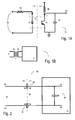
- FIG. 1A shows a known electrical isolator circuit 10 for conveying signals from a mains voltage circuit to a low voltage circuit whilst maintaining isolation between the mains and low voltage circuits.
- the electrical isolator circuit 10 comprises an opto-isolator 12 having an infrared light emitting diode (LED) 14 and a photo-transistor 16.
- a resistor, 18 in series with the LED 14 limits the current flowing through the LED 14.
- a load resistor, 20 is present in series with the photo-transistor 16 between the photo-transistor and the positive power line.
- a capacitor, Capacitor 22 represents a parasitic capacitance of the electrical circuit connected to the output 24 of the photo-transistor.
- a high voltage AC signal is applied across the inputs 26 to the electrical isolator circuit to thereby cause operation of the LED 14.
- Light emitted by the LED is received by the photo-transistor and causes a current to flow in the photo-transistor with the current developed across the load resistor to thereby provide a corresponding voltage at the output 24.
- a disadvantage of the electrical isolator circuit of Figure 1A is its high power dissipation on the low voltage side and, in particular, on the high voltage side.
- the temporal accuracy of the output 24 depends on the speed at which the isolator circuit 10 is capable of switching with the switching speed being determined by the RC time constant of resistor 20 and capacitor 22.
- the maximum value of resistor 20 can be determined for a given load and a desired accuracy.
- the maximum value of resistor 20 and the required voltage swing in turn determine the minimum required photo-transistor current, Ic.
- CTR current transfer ratio
- FIG. 1 B Another known electrical isolator circuit 1 is shown in Figure 1 B.
- the electrical isolator circuit 1 of Figure 1 B comprises a transformer 2 having a primary winding of N1 turns of conductor around a magnetic core and a secondary winding of N2 turns around the same core.
- a low voltage circuit 3 is connected across the secondary winding of the transformer 1.
- an output voltage which is proportional to the high voltage AC signal, is developed across the secondary winding and thus provided to the low voltage circuit 3.
- the output voltage (Vout) is given by N2/N1 x Vin, where Vin is the high voltage AC signal 4.
- the electrical isolator circuit 1 of Figure 1 B provides coupling of AC signals from the high voltage AC signal side to the low voltage side whilst providing for DC isolation between the high voltage AC signal side and the low voltage side.
- a disadvantage of the electrical isolator circuit 1 of Figure 1 B when used with low frequency signals, such as for the coupling of domestic mains signals, is the typically large size of the transformer.
- the transformer is normally large on account of the need for: a large transformer core to prevent saturation; and a large number of windings to minimise losses.
- a further and associated disadvantage of the electrical isolator circuit 1 of Figure 1 B is its comparatively high cost.
- Figure 2 shows an electrical isolator circuit 30 comprising an input stage 32, an output stage 34 comprising a capacitive load 36, and a DC isolator 38.
- the input stage 32 has first 40 and second 42 inputs.
- the output stage 34 has first 44 and second 46 outputs.
- the DC isolator 38 comprises first 48 and second 50 capacitors.
- a first plate 52 of the first capacitor 48 is electrically connected to the first input 40 and the second plate 54 of the first capacitor 48 is electrically connected to a first side of the capacitive load 36.
- the first side of the capacitive load 36 constitutes the first output 44.
- a first plate 56 of the second capacitor 50 is electrically connected to the second input 42 and the second plate 58 of the second capacitor 50 is electrically connected to a second, opposing side of the capacitive load 36.
- the second side of the capacitive load 36 constitutes the second output 46.
- the electrical isolator circuit also comprises a voltage source, which is operative to provide a domestic mains signal, such as 230 Vrms at 50 Hz, to the input stage.
- a detection circuit 51 is connected to the output stage at the first and second outputs. The form and function of the detection circuit depends on the application to hand.
- the detection circuit may be a zero-crossing detector, where the integrity of the mains is being monitored, or an analogue to digital converter with associated processing circuitry, where the voltage level of the mains is being measured.
- the design of such circuits is within the scope of the ordinary design capabilities of the skilled person.
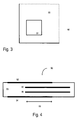
- FIGS 3 and 4 show respectively plan and cross-section views of the physical arrangement of capacitors 36, 48, 50 of Figure 2 .
- Each of the plates of the capacitor are defined by respective metal layers on the top and bottom surfaces 92, 94, and embedded within 96, 98" the printed circuit board 68.
- the metal layers are disposed such that they at least partially overlap and so that the non-conductive substrate 68 of the printed circuit board defines the dielectric of the capacitor.
- the formation of metal tracks and of larger area structures, such the metal layers of the first and second plates, on a printed circuit board substrate is a process that is well known to the skilled person.
- one or more capacitor plates are defined by metal layers embedded within the substrate.
- the provision of embedded metal tracks and of larger area structures, such the metal layers of the first and second plates, is a process that is well known to the skilled person.
- the first capacitor 48 is defined by a first surface layer 92 on a first surface of the printed circuit board 68 and a first embedded layer 96 within the printed circuit board, these layers being at least partially overlapping such that each forms one of plates 52, 54 of the capacitor 48.
- capacitor 50 is defined by a second surface layer 94 on a second surface of the printed circuit board 68 and a second embedded layer 98 within the printed circuit board, these layers being at least partially overlapping such that each forms one of plates 56, 58 of the capacitor 50.
- the dielectric is defined by the part of the substrate 68 between the relevant layers.
- the capacitive electrical load 36 is defined by the first and second embedded layers 96, 98, which are spaced apart from each other, the dielectric again being defined by the substrate; more specifically, the part of the substrate between the first and second embedded layers 96, 98
- a domestic mains signal is applied to the input stage of 32 of the electrical isolator circuit 30 of Figure 2 .
- the configuration of the first 48 and second 50 capacitors is such that they form a potential divider with the electrical load 36 to provide an attenuated representation of the domestic mains voltage signal across the electrical load.
- a value of substantially 5 pF is used for each of the first and second capacitors along with an electrical load having a capacitance of substantially 200 pF to provide an attenuated voltage across the electrical load of about 5 volts.
- the first 96 and second 98 embedded layers may be spaced apart from each other to an extent less than the spacing between each of the first surface layer 92 and the first embedded layer 96 and of the second surface layer 94 and the second embedded layer 98.
- the two embedded layers 96, 98 may only partially overlap the two surface layers 92, 94. Therefore the area of overlap 95 of the plates making up the first and second capacitors 48, 50 is substantially smaller than the area of overlap (the entire plate area in this example) of the plates making up the load capacitor 36.
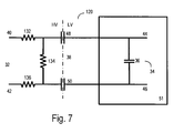
- FIGS 5 to 7 show circuit diagrams of an electrical isolator according to the present invention having three different forms of input stage. Components in common with the circuit of Figure 2 are identified with common reference numerals. The reader's attention is directed to the description given with reference to Figure 2 for a description of the form and function of such components.
- the circuit 110 of Figure 5 comprises a diode 112 in series with the first capacitor 48, the diode being operative as a rectifier.
- the circuit 120 of Figure 5 comprises a bridge rectifier 122 between the input connections of the input stage 32 and the first and second capacitors 48, 50. The bridge rectifier 122 is operative to full wave rectify the domestic mains signal applied to the input stage.
- the circuit 130 of Figure 7 comprises a resistive divider formed of series connected first 132, second 134 and third 136 resistors.
- the first plates of each of the first and second capacitors 48, 50 are connected to opposing ends of the second resistance 134 to thereby provide an attenuated form of the domestic mains voltage signal to the first and second capacitors.
- the values of the first 132, second 134 and third 136 resistors are chosen depending on the level of the domestic mains voltage signal and the voltage level desired to be applied to the first and second capacitors.
Landscapes
- Engineering & Computer Science (AREA)
- Power Engineering (AREA)
- Computer Networks & Wireless Communication (AREA)
- Signal Processing (AREA)
- Microelectronics & Electronic Packaging (AREA)
- Rectifiers (AREA)
- Dc-Dc Converters (AREA)
Claims (12)
- Elektrische Isolatorschaltung mit:einer Eingangsstufe, die einen ersten (40) und einen zweiten (42) Eingang aufweist, wobei die Eingangsstufe dazu konfiguriert ist, ein Eingangsspannungssignal zu empfangen, nämlich ein Wechselstrom-Netzspannungssignal;einer Ausgangsstufe, die einen ersten (44) und einen zweiten (46) Ausgang aufweist, die über einen Lastkondensator elektrisch verbunden sind; undeinen Gleichstromisolator, der einen ersten Kondensator (48) zwischen dem ersten Eingang und dem ersten Ausgang und einen zweiten Kondensator (50) zwischen dem zweiten Eingang und dem zweiten Ausgang aufweist;wobeierste und zweite Platten von jeweils dem ersten, dem zweiten und dem Lastkondensator durch leitende Schichten einer gedruckten Leiterplatte definiert sind und das Dielektrikum von jeweils dem ersten, dem zweiten und dem Lastkondensator durch ein nichtleitendes Teil (68) der gedruckten Leiterplatte definiert ist;wobei der erste, der zweite und der Lastkondensator durch vier der leitenden Schichten definiert sind, die einander jeweils teilweise überlappen, so dass eine der leitenden Schichten eine erste der Platten des Lastkondensators und eine der Platten des ersten Kondensators definiert, und eine andere der leitenden Schichten eine zweite der Platten des Lastkondensators und eine der Platten des zweiten Kondensators definiert;wobei die erste Platte des ersten Kondensators durch eine erste Oberflächenschicht (92) auf einer ersten Oberfläche der gedruckten Leiterplatte (68) definiert ist, die erste Platte des zweiten Kondensators durch eine zweite Oberflächenschicht (94) auf einer zweiten gegenüberliegenden Oberfläche der gedruckten Leiterplatte definiert ist, die zweite Platte des ersten Kondensators und die erste Platte des Lastkondensators beide durch eine erste eingebettete Schicht in der gedruckten Leiterplatte definiert sind, und die zweite Platte des zweiten Kondensators und die zweite Platte des Lastkondensators beide durch eine zweite eingebettete Schicht definiert sind, wobei die erste und die zweite eingebettete Schicht voneinander beabstandet sind;wobei die erste und die zweite Oberflächenschicht die erste und die zweite eingebettete Schicht nur teilweise überlappen, während die erste und die zweite eingebettete Schicht (96, 98) einander vollständig überlappen, so dass der Überlappungsbereich der Schichten, die den ersten und zweiten Kondensator definieren, kleiner ist, als der Überlappungsbereich der Schichten, die den Lastkondensator definieren, um eine abgeschwächte Repräsentation des Netzspannungssignals über den Lastkondensator bereitzustellen.
- Elektrische Isolatorschaltung nach Anspruch 1, wobei die erste und die zweite eingebettete Schicht voneinander in geringerem Ausmaß beabstandet sind, als der Abstand zwischen jeder der ersten Oberflächenschicht und der ersten eingebetteten Schicht und der zweiten Oberflächenschicht und der zweiten eingebetteten Schicht beträgt.
- Elektrische Isolatorschaltung nach einem der Ansprüche 1 bis 2, wobei die eingebetteten Schichten jeweils ähnliche Bereiche und Ausmaße haben.
- Elektrische Isolatorschaltung nach einem der vorhergehenden Ansprüche, wobei der erste und der zweite Kondensator so konfiguriert sind, dass der erste und der zweite Kondensator einen Potenzialteiler mit dem Lastkondensator bilden.
- Elektrische Isolatorschaltung nach einem der vorhergehenden Ansprüche, wobei die Eingangsstufe dazu konfiguriert ist, ein Wechselstrom-Hochspannungssignal zu empfangen, das eine Frequenz von weniger als 500 Hz hat.
- Elektrische Isolatorschaltung nach Anspruch 5, wobei ein Wechselstrom-Hochspannungssignal eine Wechselstromspannung von 50 Vrms oder größer ist.
- Elektrische Isolatorschaltung nach einem der vorhergehenden Ansprüche, wobei die Ausgangsstufe bei einer Niedrigspannung von wenigstens einem einer Wechselstromspannung von weniger als 50 Vrms und einer Gleichstromspannung von weniger als 120 Volt betreibbar ist.
- Elektrische Isolatorschaltung nach Anspruch 7, wobei das Niedrigspannungssignal eine Gleichstromspannung von weniger als im Wesentlichen 15 Volt ist.
- Elektrische Isolatorschaltung nach einem der vorhergehenden Ansprüche, wobei jeder des ersten und des zweiten Kondensators eine Kapazität von weniger als 100 pF hat.
- Elektrische Isolatorschaltung nach einem der vorhergehenden Ansprüche, wobei der Lastkondensator eine Kapazität zwischen im Wesentlichen 20 pF und im Wesentlichen 1 nF hat.
- Elektrische Isolatorschaltung nach einem der vorhergehenden Ansprüche, wobei die Eingangsstufe eine Gleichrichterschaltung aufweist, die dazu betreibbar ist, ein Wechselstrom-Hochspannungssignal gleichzurichten, bevor es den Gleichstromisolator erreicht.
- Elektrische Isolatorschaltung nach einem der vorhergehenden Ansprüche, wobei die Eingangsstufe einen Widerstandsteiler aufweist, der dazu betreibbar ist, den Spannungspegel eines Wechselstrom-Hochspannungssignals, das an die Eingangsstufe angelegt wird, zu reduzieren.
Applications Claiming Priority (2)
| Application Number | Priority Date | Filing Date | Title |
|---|---|---|---|
| GBGB0916763.6A GB0916763D0 (en) | 2009-09-24 | 2009-09-24 | Electrical isolators |
| PCT/GB2010/051598 WO2011036490A1 (en) | 2009-09-24 | 2010-09-23 | Electrical isolators |
Publications (2)
| Publication Number | Publication Date |
|---|---|
| EP2465207A1 EP2465207A1 (de) | 2012-06-20 |
| EP2465207B1 true EP2465207B1 (de) | 2013-05-15 |
Family
ID=41327513
Family Applications (1)
| Application Number | Title | Priority Date | Filing Date |
|---|---|---|---|
| EP10771167.3A Not-in-force EP2465207B1 (de) | 2009-09-24 | 2010-09-23 | Elektrische trennschaltung |
Country Status (5)
| Country | Link |
|---|---|
| US (1) | US8847574B2 (de) |
| EP (1) | EP2465207B1 (de) |
| CN (1) | CN102577149B (de) |
| GB (1) | GB0916763D0 (de) |
| WO (1) | WO2011036490A1 (de) |
Families Citing this family (4)
| Publication number | Priority date | Publication date | Assignee | Title |
|---|---|---|---|---|
| US9722729B2 (en) * | 2013-05-31 | 2017-08-01 | Qualcomm Incorporated | Extracting zero cross information in a powerline communication device |
| US10523175B2 (en) * | 2017-03-23 | 2019-12-31 | Texas Instruments Incorporated | Low loss galvanic isolation circuitry |
| EP3639043A1 (de) * | 2017-06-13 | 2020-04-22 | 3M Innovative Properties Company | Hochspannungsimpedanzanordnung |
| EP4525561A1 (de) * | 2023-09-18 | 2025-03-19 | Tridonic GmbH & Co. KG | Überbrückung einer selenv-barriere eines isolierten treibers |
Family Cites Families (4)
| Publication number | Priority date | Publication date | Assignee | Title |
|---|---|---|---|---|
| US7054372B2 (en) * | 2000-12-15 | 2006-05-30 | Lucent Technologies Inc. | Digital transmission line tap circuit |
| US7483274B2 (en) * | 2005-09-29 | 2009-01-27 | Welch Allyn, Inc. | Galvanic isolation of a signal using capacitive coupling embedded within a circuit board |
| US7791900B2 (en) * | 2006-08-28 | 2010-09-07 | Avago Technologies General Ip (Singapore) Pte. Ltd. | Galvanic isolator |
| US8159312B2 (en) | 2007-06-27 | 2012-04-17 | Medrelief Inc. | Method and system for signal coupling and direct current blocking |
-
2009
- 2009-09-24 GB GBGB0916763.6A patent/GB0916763D0/en not_active Ceased
-
2010
- 2010-09-23 US US13/498,086 patent/US8847574B2/en not_active Expired - Fee Related
- 2010-09-23 CN CN201080042439.0A patent/CN102577149B/zh not_active Expired - Fee Related
- 2010-09-23 WO PCT/GB2010/051598 patent/WO2011036490A1/en not_active Ceased
- 2010-09-23 EP EP10771167.3A patent/EP2465207B1/de not_active Not-in-force
Also Published As
| Publication number | Publication date |
|---|---|
| HK1167949A1 (en) | 2012-12-14 |
| WO2011036490A1 (en) | 2011-03-31 |
| CN102577149A (zh) | 2012-07-11 |
| EP2465207A1 (de) | 2012-06-20 |
| US8847574B2 (en) | 2014-09-30 |
| US20120230074A1 (en) | 2012-09-13 |
| GB0916763D0 (en) | 2009-11-04 |
| CN102577149B (zh) | 2014-10-01 |
Similar Documents
| Publication | Publication Date | Title |
|---|---|---|
| US20150257271A1 (en) | Signal level crossing detector circuit | |
| US9589718B2 (en) | Method for reducing or eliminating conducted common mode noise in a transformer | |
| US8847574B2 (en) | Electrical isolators | |
| US10547246B2 (en) | Auxiliary supply for a current supply | |
| US10284017B2 (en) | Coil device and wireless power transmission device | |
| CN108303579A (zh) | 一种电压检测电路和方法 | |
| EP2387153B1 (de) | Signalpegelüberschreitungsdetektorschaltung | |
| WO2009128025A1 (en) | Switched mode power supply | |
| US9647571B2 (en) | Internal inverter communications | |
| KR101776617B1 (ko) | 절연형 브릿지리스 pfc컨버터 | |
| US8779749B2 (en) | Circuit for controlling an A.C. switch | |
| WO2017089120A1 (en) | A driver circuit | |
| HK1167949B (en) | Electrical isolators | |
| RU2764282C1 (ru) | Определение входного напряжения для точки гальванической развязки | |
| CN115102387B (zh) | 一种交直流开入量的开入回路 | |
| US20180159429A1 (en) | Auxiliary Supply for a Switched-Mode Power Supply | |
| EP4048031B1 (de) | Treiber für beleuchtungsmittel | |
| WO2003023990A1 (en) | Line interface circuit for power line communication | |
| GB2474476A (en) | An isolating capacitor using a PCB layer as a dielectric | |
| JP2004239888A (ja) | 電圧検出装置 | |
| JPS60176417A (ja) | 停電検出装置 | |
| JP2004088952A (ja) | 共振型スイッチング電源 | |
| US20220349955A1 (en) | Line and neutral detection circuit | |
| HK1166132A (en) | Signal level crossing detector circuit and integrated circuit | |
| HK1165555A (en) | Signal level crossing detector circuit and integrated circuit thereof |
Legal Events
| Date | Code | Title | Description |
|---|---|---|---|
| PUAI | Public reference made under article 153(3) epc to a published international application that has entered the european phase |
Free format text: ORIGINAL CODE: 0009012 |
|
| 17P | Request for examination filed |
Effective date: 20120316 |
|
| AK | Designated contracting states |
Kind code of ref document: A1 Designated state(s): AL AT BE BG CH CY CZ DE DK EE ES FI FR GB GR HR HU IE IS IT LI LT LU LV MC MK MT NL NO PL PT RO SE SI SK SM TR |
|
| GRAP | Despatch of communication of intention to grant a patent |
Free format text: ORIGINAL CODE: EPIDOSNIGR1 |
|
| DAX | Request for extension of the european patent (deleted) | ||
| GRAS | Grant fee paid |
Free format text: ORIGINAL CODE: EPIDOSNIGR3 |
|
| GRAA | (expected) grant |
Free format text: ORIGINAL CODE: 0009210 |
|
| AK | Designated contracting states |
Kind code of ref document: B1 Designated state(s): AL AT BE BG CH CY CZ DE DK EE ES FI FR GB GR HR HU IE IS IT LI LT LU LV MC MK MT NL NO PL PT RO SE SI SK SM TR |
|
| REG | Reference to a national code |
Ref country code: GB Ref legal event code: FG4D Ref country code: CH Ref legal event code: EP |
|
| REG | Reference to a national code |
Ref country code: AT Ref legal event code: REF Ref document number: 612568 Country of ref document: AT Kind code of ref document: T Effective date: 20130615 |
|
| REG | Reference to a national code |
Ref country code: IE Ref legal event code: FG4D |
|
| REG | Reference to a national code |
Ref country code: DE Ref legal event code: R096 Ref document number: 602010007167 Country of ref document: DE Effective date: 20130711 |
|
| REG | Reference to a national code |
Ref country code: AT Ref legal event code: MK05 Ref document number: 612568 Country of ref document: AT Kind code of ref document: T Effective date: 20130515 |
|
| REG | Reference to a national code |
Ref country code: LT Ref legal event code: MG4D |
|
| REG | Reference to a national code |
Ref country code: NL Ref legal event code: VDEP Effective date: 20130515 |
|
| PG25 | Lapsed in a contracting state [announced via postgrant information from national office to epo] |
Ref country code: SI Free format text: LAPSE BECAUSE OF FAILURE TO SUBMIT A TRANSLATION OF THE DESCRIPTION OR TO PAY THE FEE WITHIN THE PRESCRIBED TIME-LIMIT Effective date: 20130515 Ref country code: NO Free format text: LAPSE BECAUSE OF FAILURE TO SUBMIT A TRANSLATION OF THE DESCRIPTION OR TO PAY THE FEE WITHIN THE PRESCRIBED TIME-LIMIT Effective date: 20130815 Ref country code: LT Free format text: LAPSE BECAUSE OF FAILURE TO SUBMIT A TRANSLATION OF THE DESCRIPTION OR TO PAY THE FEE WITHIN THE PRESCRIBED TIME-LIMIT Effective date: 20130515 Ref country code: ES Free format text: LAPSE BECAUSE OF FAILURE TO SUBMIT A TRANSLATION OF THE DESCRIPTION OR TO PAY THE FEE WITHIN THE PRESCRIBED TIME-LIMIT Effective date: 20130826 Ref country code: SE Free format text: LAPSE BECAUSE OF FAILURE TO SUBMIT A TRANSLATION OF THE DESCRIPTION OR TO PAY THE FEE WITHIN THE PRESCRIBED TIME-LIMIT Effective date: 20130515 Ref country code: IS Free format text: LAPSE BECAUSE OF FAILURE TO SUBMIT A TRANSLATION OF THE DESCRIPTION OR TO PAY THE FEE WITHIN THE PRESCRIBED TIME-LIMIT Effective date: 20130915 Ref country code: FI Free format text: LAPSE BECAUSE OF FAILURE TO SUBMIT A TRANSLATION OF THE DESCRIPTION OR TO PAY THE FEE WITHIN THE PRESCRIBED TIME-LIMIT Effective date: 20130515 Ref country code: PT Free format text: LAPSE BECAUSE OF FAILURE TO SUBMIT A TRANSLATION OF THE DESCRIPTION OR TO PAY THE FEE WITHIN THE PRESCRIBED TIME-LIMIT Effective date: 20130916 Ref country code: GR Free format text: LAPSE BECAUSE OF FAILURE TO SUBMIT A TRANSLATION OF THE DESCRIPTION OR TO PAY THE FEE WITHIN THE PRESCRIBED TIME-LIMIT Effective date: 20130816 Ref country code: AT Free format text: LAPSE BECAUSE OF FAILURE TO SUBMIT A TRANSLATION OF THE DESCRIPTION OR TO PAY THE FEE WITHIN THE PRESCRIBED TIME-LIMIT Effective date: 20130515 |
|
| PG25 | Lapsed in a contracting state [announced via postgrant information from national office to epo] |
Ref country code: PL Free format text: LAPSE BECAUSE OF FAILURE TO SUBMIT A TRANSLATION OF THE DESCRIPTION OR TO PAY THE FEE WITHIN THE PRESCRIBED TIME-LIMIT Effective date: 20130515 Ref country code: HR Free format text: LAPSE BECAUSE OF FAILURE TO SUBMIT A TRANSLATION OF THE DESCRIPTION OR TO PAY THE FEE WITHIN THE PRESCRIBED TIME-LIMIT Effective date: 20130515 Ref country code: BG Free format text: LAPSE BECAUSE OF FAILURE TO SUBMIT A TRANSLATION OF THE DESCRIPTION OR TO PAY THE FEE WITHIN THE PRESCRIBED TIME-LIMIT Effective date: 20130815 |
|
| PG25 | Lapsed in a contracting state [announced via postgrant information from national office to epo] |
Ref country code: LV Free format text: LAPSE BECAUSE OF FAILURE TO SUBMIT A TRANSLATION OF THE DESCRIPTION OR TO PAY THE FEE WITHIN THE PRESCRIBED TIME-LIMIT Effective date: 20130515 |
|
| PG25 | Lapsed in a contracting state [announced via postgrant information from national office to epo] |
Ref country code: BE Free format text: LAPSE BECAUSE OF FAILURE TO SUBMIT A TRANSLATION OF THE DESCRIPTION OR TO PAY THE FEE WITHIN THE PRESCRIBED TIME-LIMIT Effective date: 20130515 Ref country code: DK Free format text: LAPSE BECAUSE OF FAILURE TO SUBMIT A TRANSLATION OF THE DESCRIPTION OR TO PAY THE FEE WITHIN THE PRESCRIBED TIME-LIMIT Effective date: 20130515 Ref country code: EE Free format text: LAPSE BECAUSE OF FAILURE TO SUBMIT A TRANSLATION OF THE DESCRIPTION OR TO PAY THE FEE WITHIN THE PRESCRIBED TIME-LIMIT Effective date: 20130515 Ref country code: CZ Free format text: LAPSE BECAUSE OF FAILURE TO SUBMIT A TRANSLATION OF THE DESCRIPTION OR TO PAY THE FEE WITHIN THE PRESCRIBED TIME-LIMIT Effective date: 20130515 Ref country code: SK Free format text: LAPSE BECAUSE OF FAILURE TO SUBMIT A TRANSLATION OF THE DESCRIPTION OR TO PAY THE FEE WITHIN THE PRESCRIBED TIME-LIMIT Effective date: 20130515 |
|
| PG25 | Lapsed in a contracting state [announced via postgrant information from national office to epo] |
Ref country code: RO Free format text: LAPSE BECAUSE OF FAILURE TO SUBMIT A TRANSLATION OF THE DESCRIPTION OR TO PAY THE FEE WITHIN THE PRESCRIBED TIME-LIMIT Effective date: 20130515 Ref country code: NL Free format text: LAPSE BECAUSE OF FAILURE TO SUBMIT A TRANSLATION OF THE DESCRIPTION OR TO PAY THE FEE WITHIN THE PRESCRIBED TIME-LIMIT Effective date: 20130515 Ref country code: IT Free format text: LAPSE BECAUSE OF FAILURE TO SUBMIT A TRANSLATION OF THE DESCRIPTION OR TO PAY THE FEE WITHIN THE PRESCRIBED TIME-LIMIT Effective date: 20130515 |
|
| PLBE | No opposition filed within time limit |
Free format text: ORIGINAL CODE: 0009261 |
|
| STAA | Information on the status of an ep patent application or granted ep patent |
Free format text: STATUS: NO OPPOSITION FILED WITHIN TIME LIMIT |
|
| 26N | No opposition filed |
Effective date: 20140218 |
|
| PG25 | Lapsed in a contracting state [announced via postgrant information from national office to epo] |
Ref country code: MC Free format text: LAPSE BECAUSE OF FAILURE TO SUBMIT A TRANSLATION OF THE DESCRIPTION OR TO PAY THE FEE WITHIN THE PRESCRIBED TIME-LIMIT Effective date: 20130515 |
|
| REG | Reference to a national code |
Ref country code: DE Ref legal event code: R097 Ref document number: 602010007167 Country of ref document: DE Effective date: 20140218 |
|
| REG | Reference to a national code |
Ref country code: FR Ref legal event code: ST Effective date: 20140530 |
|
| REG | Reference to a national code |
Ref country code: IE Ref legal event code: MM4A |
|
| PG25 | Lapsed in a contracting state [announced via postgrant information from national office to epo] |
Ref country code: IE Free format text: LAPSE BECAUSE OF NON-PAYMENT OF DUE FEES Effective date: 20130923 |
|
| PG25 | Lapsed in a contracting state [announced via postgrant information from national office to epo] |
Ref country code: FR Free format text: LAPSE BECAUSE OF NON-PAYMENT OF DUE FEES Effective date: 20130930 |
|
| REG | Reference to a national code |
Ref country code: DE Ref legal event code: R082 Ref document number: 602010007167 Country of ref document: DE Representative=s name: BOSCH JEHLE PATENTANWALTSGESELLSCHAFT MBH, DE |
|
| REG | Reference to a national code |
Ref country code: DE Ref legal event code: R082 Ref document number: 602010007167 Country of ref document: DE Representative=s name: BOSCH JEHLE PATENTANWALTSGESELLSCHAFT MBH, DE Effective date: 20140902 Ref country code: DE Ref legal event code: R081 Ref document number: 602010007167 Country of ref document: DE Owner name: BROADCOM EUROPE LTD., CAMBRIDGE, GB Free format text: FORMER OWNER: GIGLE NETWORKS LTD., EDINBURGH, GB Effective date: 20140902 |
|
| REG | Reference to a national code |
Ref country code: CH Ref legal event code: PL |
|
| GBPC | Gb: european patent ceased through non-payment of renewal fee |
Effective date: 20140923 |
|
| PG25 | Lapsed in a contracting state [announced via postgrant information from national office to epo] |
Ref country code: SM Free format text: LAPSE BECAUSE OF FAILURE TO SUBMIT A TRANSLATION OF THE DESCRIPTION OR TO PAY THE FEE WITHIN THE PRESCRIBED TIME-LIMIT Effective date: 20130515 |
|
| PG25 | Lapsed in a contracting state [announced via postgrant information from national office to epo] |
Ref country code: CY Free format text: LAPSE BECAUSE OF FAILURE TO SUBMIT A TRANSLATION OF THE DESCRIPTION OR TO PAY THE FEE WITHIN THE PRESCRIBED TIME-LIMIT Effective date: 20130515 Ref country code: MT Free format text: LAPSE BECAUSE OF FAILURE TO SUBMIT A TRANSLATION OF THE DESCRIPTION OR TO PAY THE FEE WITHIN THE PRESCRIBED TIME-LIMIT Effective date: 20130515 Ref country code: TR Free format text: LAPSE BECAUSE OF FAILURE TO SUBMIT A TRANSLATION OF THE DESCRIPTION OR TO PAY THE FEE WITHIN THE PRESCRIBED TIME-LIMIT Effective date: 20130515 |
|
| PG25 | Lapsed in a contracting state [announced via postgrant information from national office to epo] |
Ref country code: HU Free format text: LAPSE BECAUSE OF FAILURE TO SUBMIT A TRANSLATION OF THE DESCRIPTION OR TO PAY THE FEE WITHIN THE PRESCRIBED TIME-LIMIT; INVALID AB INITIO Effective date: 20100923 Ref country code: GB Free format text: LAPSE BECAUSE OF NON-PAYMENT OF DUE FEES Effective date: 20140923 Ref country code: LU Free format text: LAPSE BECAUSE OF NON-PAYMENT OF DUE FEES Effective date: 20130923 Ref country code: MK Free format text: LAPSE BECAUSE OF FAILURE TO SUBMIT A TRANSLATION OF THE DESCRIPTION OR TO PAY THE FEE WITHIN THE PRESCRIBED TIME-LIMIT Effective date: 20130515 Ref country code: LI Free format text: LAPSE BECAUSE OF NON-PAYMENT OF DUE FEES Effective date: 20140930 Ref country code: CH Free format text: LAPSE BECAUSE OF NON-PAYMENT OF DUE FEES Effective date: 20140930 |
|
| PGFP | Annual fee paid to national office [announced via postgrant information from national office to epo] |
Ref country code: DE Payment date: 20160930 Year of fee payment: 7 |
|
| REG | Reference to a national code |
Ref country code: DE Ref legal event code: R119 Ref document number: 602010007167 Country of ref document: DE |
|
| PG25 | Lapsed in a contracting state [announced via postgrant information from national office to epo] |
Ref country code: DE Free format text: LAPSE BECAUSE OF NON-PAYMENT OF DUE FEES Effective date: 20180404 |
|
| PG25 | Lapsed in a contracting state [announced via postgrant information from national office to epo] |
Ref country code: AL Free format text: LAPSE BECAUSE OF FAILURE TO SUBMIT A TRANSLATION OF THE DESCRIPTION OR TO PAY THE FEE WITHIN THE PRESCRIBED TIME-LIMIT Effective date: 20130515 |