EP2463906A2 - Semiconductor device - Google Patents
Semiconductor device Download PDFInfo
- Publication number
- EP2463906A2 EP2463906A2 EP11170565A EP11170565A EP2463906A2 EP 2463906 A2 EP2463906 A2 EP 2463906A2 EP 11170565 A EP11170565 A EP 11170565A EP 11170565 A EP11170565 A EP 11170565A EP 2463906 A2 EP2463906 A2 EP 2463906A2
- Authority
- EP
- European Patent Office
- Prior art keywords
- high frequency
- semiconductor chip
- semiconductor device
- terminal
- disposed
- Prior art date
- Legal status (The legal status is an assumption and is not a legal conclusion. Google has not performed a legal analysis and makes no representation as to the accuracy of the status listed.)
- Granted
Links
Images





Classifications
-
- H—ELECTRICITY
- H10—SEMICONDUCTOR DEVICES; ELECTRIC SOLID-STATE DEVICES NOT OTHERWISE PROVIDED FOR
- H10W—GENERIC PACKAGES, INTERCONNECTIONS, CONNECTORS OR OTHER CONSTRUCTIONAL DETAILS OF DEVICES COVERED BY CLASS H10
- H10W76/00—Containers; Fillings or auxiliary members therefor; Seals
- H10W76/10—Containers or parts thereof
- H10W76/12—Containers or parts thereof characterised by their shape
- H10W76/13—Containers comprising a conductive base serving as an interconnection
- H10W76/134—Containers comprising a conductive base serving as an interconnection having other interconnections parallel to the conductive base
-
- H—ELECTRICITY
- H10—SEMICONDUCTOR DEVICES; ELECTRIC SOLID-STATE DEVICES NOT OTHERWISE PROVIDED FOR
- H10W—GENERIC PACKAGES, INTERCONNECTIONS, CONNECTORS OR OTHER CONSTRUCTIONAL DETAILS OF DEVICES COVERED BY CLASS H10
- H10W44/00—Electrical arrangements for controlling or matching impedance
- H10W44/20—Electrical arrangements for controlling or matching impedance at high-frequency [HF] or radio frequency [RF]
-
- H—ELECTRICITY
- H10—SEMICONDUCTOR DEVICES; ELECTRIC SOLID-STATE DEVICES NOT OTHERWISE PROVIDED FOR
- H10W—GENERIC PACKAGES, INTERCONNECTIONS, CONNECTORS OR OTHER CONSTRUCTIONAL DETAILS OF DEVICES COVERED BY CLASS H10
- H10W44/00—Electrical arrangements for controlling or matching impedance
- H10W44/601—Capacitive arrangements
-
- H—ELECTRICITY
- H10—SEMICONDUCTOR DEVICES; ELECTRIC SOLID-STATE DEVICES NOT OTHERWISE PROVIDED FOR
- H10D—INORGANIC ELECTRIC SEMICONDUCTOR DEVICES
- H10D30/00—Field-effect transistors [FET]
- H10D30/40—FETs having zero-dimensional [0D], one-dimensional [1D] or two-dimensional [2D] charge carrier gas channels
- H10D30/47—FETs having zero-dimensional [0D], one-dimensional [1D] or two-dimensional [2D] charge carrier gas channels having two-dimensional [2D] charge carrier gas channels, e.g. nanoribbon FETs or high electron mobility transistors [HEMT]
- H10D30/471—High electron mobility transistors [HEMT] or high hole mobility transistors [HHMT]
- H10D30/475—High electron mobility transistors [HEMT] or high hole mobility transistors [HHMT] having wider bandgap layer formed on top of lower bandgap active layer, e.g. undoped barrier HEMTs such as i-AlGaN/GaN HEMTs
-
- H—ELECTRICITY
- H10—SEMICONDUCTOR DEVICES; ELECTRIC SOLID-STATE DEVICES NOT OTHERWISE PROVIDED FOR
- H10D—INORGANIC ELECTRIC SEMICONDUCTOR DEVICES
- H10D30/00—Field-effect transistors [FET]
- H10D30/80—FETs having rectifying junction gate electrodes
- H10D30/87—FETs having Schottky gate electrodes, e.g. metal-semiconductor FETs [MESFET]
-
- H—ELECTRICITY
- H10—SEMICONDUCTOR DEVICES; ELECTRIC SOLID-STATE DEVICES NOT OTHERWISE PROVIDED FOR
- H10D—INORGANIC ELECTRIC SEMICONDUCTOR DEVICES
- H10D62/00—Semiconductor bodies, or regions thereof, of devices having potential barriers
- H10D62/80—Semiconductor bodies, or regions thereof, of devices having potential barriers characterised by the materials
- H10D62/85—Semiconductor bodies, or regions thereof, of devices having potential barriers characterised by the materials being Group III-V materials, e.g. GaAs
- H10D62/8503—Nitride Group III-V materials, e.g. AlN or GaN
-
- H—ELECTRICITY
- H10—SEMICONDUCTOR DEVICES; ELECTRIC SOLID-STATE DEVICES NOT OTHERWISE PROVIDED FOR
- H10D—INORGANIC ELECTRIC SEMICONDUCTOR DEVICES
- H10D64/00—Electrodes of devices having potential barriers
- H10D64/20—Electrodes characterised by their shapes, relative sizes or dispositions
- H10D64/23—Electrodes carrying the current to be rectified, amplified, oscillated or switched, e.g. sources, drains, anodes or cathodes
- H10D64/251—Source or drain electrodes for field-effect devices
- H10D64/257—Source or drain electrodes for field-effect devices for lateral devices wherein the source or drain electrodes are characterised by top-view geometrical layouts, e.g. interdigitated, semi-circular, annular or L-shaped electrodes
-
- H—ELECTRICITY
- H10—SEMICONDUCTOR DEVICES; ELECTRIC SOLID-STATE DEVICES NOT OTHERWISE PROVIDED FOR
- H10D—INORGANIC ELECTRIC SEMICONDUCTOR DEVICES
- H10D64/00—Electrodes of devices having potential barriers
- H10D64/20—Electrodes characterised by their shapes, relative sizes or dispositions
- H10D64/27—Electrodes not carrying the current to be rectified, amplified, oscillated or switched, e.g. gates
- H10D64/311—Gate electrodes for field-effect devices
- H10D64/411—Gate electrodes for field-effect devices for FETs
-
- H—ELECTRICITY
- H10—SEMICONDUCTOR DEVICES; ELECTRIC SOLID-STATE DEVICES NOT OTHERWISE PROVIDED FOR
- H10W—GENERIC PACKAGES, INTERCONNECTIONS, CONNECTORS OR OTHER CONSTRUCTIONAL DETAILS OF DEVICES COVERED BY CLASS H10
- H10W44/00—Electrical arrangements for controlling or matching impedance
- H10W44/20—Electrical arrangements for controlling or matching impedance at high-frequency [HF] or radio frequency [RF]
- H10W44/203—Electrical connections
- H10W44/206—Wires
-
- H—ELECTRICITY
- H10—SEMICONDUCTOR DEVICES; ELECTRIC SOLID-STATE DEVICES NOT OTHERWISE PROVIDED FOR
- H10W—GENERIC PACKAGES, INTERCONNECTIONS, CONNECTORS OR OTHER CONSTRUCTIONAL DETAILS OF DEVICES COVERED BY CLASS H10
- H10W44/00—Electrical arrangements for controlling or matching impedance
- H10W44/20—Electrical arrangements for controlling or matching impedance at high-frequency [HF] or radio frequency [RF]
- H10W44/226—Electrical arrangements for controlling or matching impedance at high-frequency [HF] or radio frequency [RF] for HF amplifiers
- H10W44/231—Arrangements for applying bias
-
- H—ELECTRICITY
- H10—SEMICONDUCTOR DEVICES; ELECTRIC SOLID-STATE DEVICES NOT OTHERWISE PROVIDED FOR
- H10W—GENERIC PACKAGES, INTERCONNECTIONS, CONNECTORS OR OTHER CONSTRUCTIONAL DETAILS OF DEVICES COVERED BY CLASS H10
- H10W44/00—Electrical arrangements for controlling or matching impedance
- H10W44/20—Electrical arrangements for controlling or matching impedance at high-frequency [HF] or radio frequency [RF]
- H10W44/226—Electrical arrangements for controlling or matching impedance at high-frequency [HF] or radio frequency [RF] for HF amplifiers
- H10W44/234—Arrangements for impedance matching
-
- H—ELECTRICITY
- H10—SEMICONDUCTOR DEVICES; ELECTRIC SOLID-STATE DEVICES NOT OTHERWISE PROVIDED FOR
- H10W—GENERIC PACKAGES, INTERCONNECTIONS, CONNECTORS OR OTHER CONSTRUCTIONAL DETAILS OF DEVICES COVERED BY CLASS H10
- H10W44/00—Electrical arrangements for controlling or matching impedance
- H10W44/20—Electrical arrangements for controlling or matching impedance at high-frequency [HF] or radio frequency [RF]
- H10W44/241—Electrical arrangements for controlling or matching impedance at high-frequency [HF] or radio frequency [RF] for passive devices or passive elements
- H10W44/243—Electrical arrangements for controlling or matching impedance at high-frequency [HF] or radio frequency [RF] for passive devices or passive elements for decoupling, e.g. bypass capacitors
-
- H—ELECTRICITY
- H10—SEMICONDUCTOR DEVICES; ELECTRIC SOLID-STATE DEVICES NOT OTHERWISE PROVIDED FOR
- H10W—GENERIC PACKAGES, INTERCONNECTIONS, CONNECTORS OR OTHER CONSTRUCTIONAL DETAILS OF DEVICES COVERED BY CLASS H10
- H10W44/00—Electrical arrangements for controlling or matching impedance
- H10W44/20—Electrical arrangements for controlling or matching impedance at high-frequency [HF] or radio frequency [RF]
- H10W44/255—Electrical arrangements for controlling or matching impedance at high-frequency [HF] or radio frequency [RF] for operation at multiple different frequencies
-
- H—ELECTRICITY
- H10—SEMICONDUCTOR DEVICES; ELECTRIC SOLID-STATE DEVICES NOT OTHERWISE PROVIDED FOR
- H10W—GENERIC PACKAGES, INTERCONNECTIONS, CONNECTORS OR OTHER CONSTRUCTIONAL DETAILS OF DEVICES COVERED BY CLASS H10
- H10W72/00—Interconnections or connectors in packages
- H10W72/50—Bond wires
- H10W72/541—Dispositions of bond wires
- H10W72/5445—Dispositions of bond wires being orthogonal to a side surface of the chip, e.g. parallel arrangements
-
- H—ELECTRICITY
- H10—SEMICONDUCTOR DEVICES; ELECTRIC SOLID-STATE DEVICES NOT OTHERWISE PROVIDED FOR
- H10W—GENERIC PACKAGES, INTERCONNECTIONS, CONNECTORS OR OTHER CONSTRUCTIONAL DETAILS OF DEVICES COVERED BY CLASS H10
- H10W72/00—Interconnections or connectors in packages
- H10W72/50—Bond wires
- H10W72/541—Dispositions of bond wires
- H10W72/547—Dispositions of multiple bond wires
- H10W72/5473—Dispositions of multiple bond wires multiple bond wires connected to a common bond pad
-
- H—ELECTRICITY
- H10—SEMICONDUCTOR DEVICES; ELECTRIC SOLID-STATE DEVICES NOT OTHERWISE PROVIDED FOR
- H10W—GENERIC PACKAGES, INTERCONNECTIONS, CONNECTORS OR OTHER CONSTRUCTIONAL DETAILS OF DEVICES COVERED BY CLASS H10
- H10W72/00—Interconnections or connectors in packages
- H10W72/50—Bond wires
- H10W72/541—Dispositions of bond wires
- H10W72/547—Dispositions of multiple bond wires
- H10W72/5475—Dispositions of multiple bond wires multiple bond wires connected to common bond pads at both ends of the wires
-
- H—ELECTRICITY
- H10—SEMICONDUCTOR DEVICES; ELECTRIC SOLID-STATE DEVICES NOT OTHERWISE PROVIDED FOR
- H10W—GENERIC PACKAGES, INTERCONNECTIONS, CONNECTORS OR OTHER CONSTRUCTIONAL DETAILS OF DEVICES COVERED BY CLASS H10
- H10W76/00—Containers; Fillings or auxiliary members therefor; Seals
- H10W76/60—Seals
-
- H—ELECTRICITY
- H10—SEMICONDUCTOR DEVICES; ELECTRIC SOLID-STATE DEVICES NOT OTHERWISE PROVIDED FOR
- H10W—GENERIC PACKAGES, INTERCONNECTIONS, CONNECTORS OR OTHER CONSTRUCTIONAL DETAILS OF DEVICES COVERED BY CLASS H10
- H10W76/00—Containers; Fillings or auxiliary members therefor; Seals
- H10W76/60—Seals
- H10W76/67—Seals characterised by their materials
-
- H—ELECTRICITY
- H10—SEMICONDUCTOR DEVICES; ELECTRIC SOLID-STATE DEVICES NOT OTHERWISE PROVIDED FOR
- H10W—GENERIC PACKAGES, INTERCONNECTIONS, CONNECTORS OR OTHER CONSTRUCTIONAL DETAILS OF DEVICES COVERED BY CLASS H10
- H10W90/00—Package configurations
- H10W90/701—Package configurations characterised by the relative positions of pads or connectors relative to package parts
- H10W90/751—Package configurations characterised by the relative positions of pads or connectors relative to package parts of bond wires
- H10W90/754—Package configurations characterised by the relative positions of pads or connectors relative to package parts of bond wires between a chip and a stacked insulating package substrate, interposer or RDL
Definitions
- Embodiments described herein generally relate to a semiconductor device.
- a resin-sealed type and a sealed and airtight type are known as a package utilized for a semiconductor element.
- the resin-sealed type semiconductor device has a structure which embedded directly the semiconductor element mounted in a leadframe in the resin by using a transfer mold etc., and is widely used by the advantage, such as low cost, being suitable for mass production, and a miniaturization being possible.
- the sealed and airtight type semiconductor device has a structure which performed in hollow airtight maintenance of the semiconductor element mounted on a base substance composed of conductive materials, such as copper. Although the cost is higher compared with the resin-sealed type semiconductor device, the sealed and airtight type semiconductor device is used when high reliability is required because of excellent in airtightness.
- the difference frequency component occurs.
- the difference frequency is several MHz
- the voltage of output terminal and the voltage of chip end face are smoothed by connecting a capacitor which is not less than 100 micro F near an RF output terminal.
- the capacitor connected near the RF output terminal cannot smooth the voltage of the chip end face, since a matching circuit intervenes between the chip end face and the capacitor.
- a semiconductor device includes a high frequency semiconductor chip, an input matching circuit, an output matching circuit, a high frequency input terminal, a high frequency output terminal, and a smoothing capacitor terminal.
- the input matching circuit is disposed at the input side of the high frequency semiconductor chip.
- the output matching circuit is disposed at the output side of the high frequency semiconductor chip.
- the high frequency input terminal is connected to the input matching circuit.
- the high frequency output terminal is connected to the output matching circuit.
- the smoothing capacitor terminal is connected to the high frequency semiconductor chip.
- the high frequency semiconductor chip, the input matching circuit, and the output matching circuit are housed by one package.
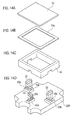
- FIG. 1 shows a schematic bird's-eye view configuration of a package for mounting a semiconductor device 1 according to an embodiment.
- a metal cap 10 is expressed as shown in FIG. 1A .
- a metal seal ring 14a is expressed as shown in FIG. 1B
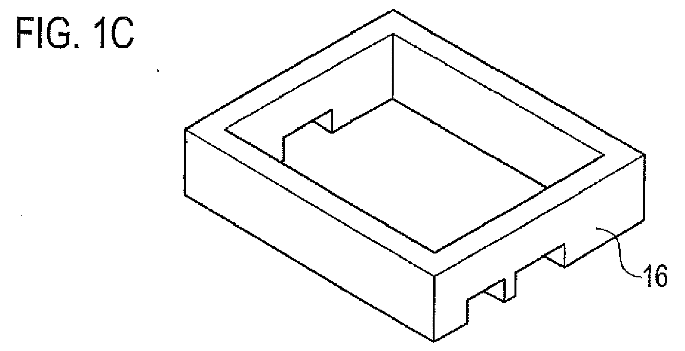
- a metal wall 16 is expressed as shown in FIG. 1C .
- a conductive base plate 200, and an input feed through 19a, an output feed through 19b and a feed through 39b utilized for capacitor disposed on an input side insulating layer 20a, an output side insulating layer 20b and an insulating layer 40b utilized for capacitor terminal are expressed as shown in FIG. 1D .
- the package for mounting the semiconductor device 1 includes: a metal cap 10; a metal seal ring 14a; a metallic wall 16; a conductive base plate 200; an input side insulating layer 20a, an output side insulating layer 20b and an insulating layer 40b utilized for capacitor terminal disposed on the conductive base plate 200; an input feed through 19a disposed on the input side insulating layer 20a; an output feed through 19b disposed on the output side insulating layer 20b; a feed through 39b utilized for capacitor disposed on the insulating layer 40b utilized for capacitor terminal; and upper layer feed throughs 22 disposed on the input side insulating layer 20a, the output side insulating layer 20b and the insulating layer 40b utilized for capacitor terminal.
- the conductive base plate 200 is formed of conductive metals, such as copper and a copper molybdenum alloy, for example. Furthermore, electroplated conductors, such as Au, Ni, Ag, an Ag-Pt alloy and an Ag-Pd alloy, may be formed on the surface of the conductive base plate 200, for example. Also, layered structure, such as Cu/Mo/Mo substrate, may be used for the conductive base plate 200.
- the metallic wall 16 As a material of the metallic wall 16, it is formed of conductive metals, such as aluminum, molybdenum, and a copper molybdenum alloy, for example.
- a soldering metal layer (not shown) for soldering is formed on the top surface of the metallic wall 16 via the metal seal ring 14a.
- the solder metal layer can be formed of a gold germanium alloy, a gold tin alloy, etc., for example.
- the metallic wall 16 is disposed on the conductive base plate 200 via a conductive adhesive material.
- the metal wall 16 is disposed on the convex upper layer feed through 22, in the feed-through portion (refer to FIG. 1 and FIG. 3 ).
- Each of the convex upper layer feed throughs 22 is disposed on the input side insulating layer 20a and the output side insulating layer 20b and the insulating layer 40b utilized for capacitor terminal, respectively, and is formed by an insulating layer.
- the input side insulating layer 20a, the output side insulating layer 20b and the insulating layer 40b utilized for capacitor terminal are equivalent to a lower layer feed through.
- the insulating adhesive material can be formed of an epoxy resin, glass, etc., for example, and the conductive adhesive material can be formed of a gold germanium alloy, a gold tin alloy, etc., for example.
- the metal cap 10 has a flat plate shape as shown in FIG. 1A .
- the metal cap 10 is disposed on the metallic wall 16 via the metal seal ring 14a.
- the package for mounting the semiconductor device 1 according to the embodiment has a high frequency characteristics of not less than 2 GHz. Accordingly, the package according to the first embodiment is applicable as a package for devices and component parts having high frequency (that is, frequency over 2 GHz).
- a schematic planar pattern configuration of the semiconductor device 1 according to the embodiment is expressed as shown in FIG. 2
- a schematic cross-section structure taken in the line I-I of FIG. 2 is expressed as shown in FIG. 3
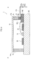
- a schematic cross-section structure taken in the line II-II of FIG. 2 is expressed as shown in FIG. 4
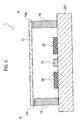
- a schematic cross-section structure taken in the line III-III of FIG. 2 is expressed as shown in FIG. 5 .
- the semiconductor device 1 includes: a high frequency semiconductor chip 24; an input matching circuit 17 disposed at the input side of the high frequency semiconductor chip 24; an output matching circuit 18 disposed at the output side of the high frequency semiconductor chip 24; a high frequency input terminal 21 a connected to the input matching circuit 17; a high frequency output terminal 21 b connected to the output matching circuit 18; and a smoothing capacitor terminal 41 b connected to the high frequency semiconductor chip 24.
- the high frequency semiconductor chip 24, the input matching circuit 17 and the output matching circuit 18 are housed by one package.
- the semiconductor device 1 includes a bypass reservoir capacitor (smoothing capacitor) C BR connected between the smoothing capacitor terminal 41 b and the ground potential (earth potential).
- the semiconductor device 1 includes the feed through 39b utilized for capacitor connected to the high frequency semiconductor chip 24, as shown in FIG. 2 and FIG. 3 .
- the smoothing capacitor terminal 41 b is connected to the drain terminal electrode D of the high frequency semiconductor chip 24 via the feed through 39b utilized for capacitor.
- the semiconductor device 1 includes a bonding wire BW1 for connecting smoothing capacitor which connects between a drain terminal electrode D of the high frequency semiconductor chip 24, and the feed through 39b utilized for capacitor.
- the semiconductor device 1 includes the input feed through 19a connected to the input matching circuit 17, and the high frequency input terminal 21 a is connected to a gate terminal electrode G of the high frequency semiconductor chip 24 via the input feed through 19a.
- the semiconductor device 1 includes the output feed through 19b connected to the output matching circuit 18, and the high frequency output terminal 21 b is connected to the drain terminal electrode D of the high frequency semiconductor chip 24 via the output feed through 19b.
- the high frequency output terminal 21 b and the smoothing capacitor terminal 41 b may be disposed to adjoin each other.
- the semiconductor device 1 includes: the high frequency semiconductor chip 24 disposed on the conductive base plate 200; an input circuit substrate 26 disposed on the conductive base plate 200 at the input side of the high frequency semiconductor chip 24; and an output circuit substrate 28 disposed on the conductive base plate 200 at the output side of the high frequency semiconductor chip 24.
- the input matching circuit 17 is disposed on the input circuit substrate 26. Moreover, the output matching circuit 18 is disposed on the output circuit substrate 28.
- the input matching circuit 17 is connected to the gate terminal electrode G of the high frequency semiconductor chip 24 via the bonding wire 12 and the output matching circuit 18 is connected to the drain terminal electrode D of the high frequency semiconductor chip 24 via the bonding wire 14.
- the high frequency input terminal 21a is connected to the input feed through 19a, and the high frequency output terminal 21 b is connected to the output feed through 19b.
- the high frequency input terminal 21a is connected to the gate terminal electrode G of the high frequency semiconductor chip 24 via the input feed through 19a, the bonding wire 11 and the input matching circuit 17.
- a schematic circuit configuration of the semiconductor device 1 includes: the high frequency semiconductor chip 24; the input matching circuit 17 disposed at the input side of the high frequency semiconductor chip 24; the output matching circuit 18 disposed at the output side of the high frequency semiconductor chip 24; the input feed through 19a connected to the input matching circuit 17; the high frequency input terminal 21a connected to the input feed through 19a; the output feed through 19b connected to the output matching circuit 18; the high frequency output terminal 21 b connected to the output feed through 99b; a capacitor connection circuit 80 disposed at the output side of the high frequency semiconductor chip 24; and the smoothing capacitor terminal 41 b connected to the capacitor connection circuit 80.
- the high frequency semiconductor chip 24, the input matching circuit 17 and the output matching circuit 18 are housed by one package surrounded by the metal wall 16.
- the capacitor connection circuit 80 includes a bonding wire BW1 for connecting smoothing capacitor which connects between the drain terminal electrode D of the high frequency semiconductor chip 24 and the feed through 39b utilized for capacitor.
- the electrode of one side of the smoothing capacitor C BR is connected to the smoothing capacitor terminal 41 b via a bonding wire for connecting smoothing capacitor BW2, and the electrode of another side of the smoothing capacitor C BR is connected to the ground potential via a bonding wire for connecting smoothing capacitor BW3.
- the semiconductor device 1 includes the smoothing capacitor terminal 41 b, and the smoothing capacitor terminal 41 b is connected with the drain terminal electrode D of the high frequency semiconductor chip 24 via the feed through 39b utilized for capacitor and the bonding wire BW1 for connecting smoothing capacitor.
- the smoothing capacitor terminal 41 b is connected with the drain terminal electrode D of the high frequency semiconductor chip 24 via the feed through 39b utilized for capacitor and the bonding wire BW1 for connecting smoothing capacitor.
- FIG. 7 shows a simulation result showing the relationship between the ripple voltage ⁇ V applying a current amplitude I PK as a parameter, and the bypass reservoir capacitor (smoothing capacitor) C BR , in the semiconductor device 1 according to the embodiment.
- FIG. 7 shows an example that the difference frequency ⁇ f is equal to 5 MHz.
- the value of not less than 0.1 ⁇ F is needed for the bypass reservoir capacitor C BR .
- the difference frequency ⁇ f is 50 MHz and the current amplitude I PK is 1.0A
- the value of not less than 0.3 ⁇ F is needed for the bypass reservoir capacitor C BR .
- the difference frequency ⁇ f is 50 MHz and the current amplitude I PK is 3.0A
- the value of not less than 1.0 ⁇ F is needed for the bypass reservoir capacitor C BR .
- FIG. 8 shows a simulation result showing the relationship between the ripple voltage ⁇ V applying the difference frequency ⁇ f as a parameter, and the bypass reservoir capacitor (smoothing capacitor) C BR .
- the semiconductor device 1 connects between the end face of drain terminal electrode D of the high frequency semiconductor chip 24 and the bypass reservoir capacitor (smoothing capacitor) C BR at the shortest, and thereby the inductance between the end face of drain terminal electrode D of the high frequency semiconductor chip 24 and the bypass reservoir capacitor C BR can be reduced to the minimum.
- third order intermodulation distortion IM3 when two frequencies are inputted into the one semiconductor device 1, the difference frequency component occurs.
- the third order intermodulation distortion IM3 has notated the signal level by the ratio to the signal level of the fundamental wave (f1 or f2).
- third order intermodulation distortion IM3 In the basic measuring method of third order intermodulation distortion IM3, two fundamental wave signals are mixed and used for the semiconductor device 1 as an input signal.
- the third order intermodulation distortion IM3 occurred with the semiconductor device 1 is measured by a spectrum analyzer.
- the output voltage and the voltage of the end face of drain of the high frequency semiconductor chip 24 are smoothed by connecting a capacitor having electrostatic capacity of not less than 100 ⁇ F near the RF output terminal.
- the voltage which appears in the end face of drain .of the high frequency semiconductor chip 24 is modulated, thereby causing a negative effect on the amplification characteristics of the semiconductor device 1.
- a reactance inductance L
- the modulated voltage amplitude is expressed by 2 ⁇ f ⁇ L ⁇ l where the alternating current of the frequency component f is I.
- the effective bias power supply source is close to the high frequency semiconductor chip 24 by disposing the bypass reservoir capacitor C BR near the high frequency semiconductor chip 24, and therefore the reactance between the bias power supply source and the end face of drain of the high frequency semiconductor chip 24 can be kept small.
- the voltage of the end face of drain of the high frequency semiconductor chip 24 is the voltage of the end face of drain terminal electrode D of the high frequency semiconductor chip 24.
- the reason for connecting the drain terminal electrode D of the high frequency semiconductor chip 24 and the feed through 39b utilized for capacitor via the bonding wire BW1 for connecting smoothing capacitor is that connecting by the wire bonding is the optimum choice since the effective electric length is short.
- the semiconductor device since it is connected without via the output matching circuit, it can be provide the semiconductor device which can smooth the voltage of the end face of drain of the high frequency semiconductor chip even when the difference frequency ⁇ f is several hundreds of MHz, and can be applied to the high frequency of the microwave/millimeter wave/submillimeter wave band.
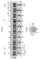
- FIG. 9A An enlarged drawing of a schematic planar pattern configuration of the high frequency semiconductor chip 24 applied to the semiconductor device 1 according to the embodiment is expressed as shown in FIG. 9A
- FIG. 9B An enlarged drawing of a part J of FIG. 9A is expressed as shown in FIG. 9B .
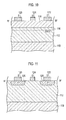
- configuration examples 1-4 of the high frequency semiconductor chip 24 applied to the semiconductor device 1 according to the embodiment, and schematic cross section configuration examples 1-4 taken in the line IV-IV of FIG. 9B are expressed as shown in FIG. 10 to FIG. 13 , respectively.
- a plurality of FET cells FET 1 to FET 10 include: a semi-insulating substrate 110; a gate finger electrode 124, a source finger electrode 120, and a drain finger electrode 122 which are disposed on a first surface of the semi-insulating substrate 110, and have a plurality of fingers, respectively; a plurality of gate terminal electrodes G1, G2, ..., G10, a plurality of source terminal electrodes S11, S12, S21, S22, ..., S101, and S102 and the drain terminal electrodes D1, D2, ..., D10 which are disposed on the first surface of the semi-insulating substrate 110, and ties a plurality of fingers, respectively every the gate finger electrode 124, the source finger electrode 120, and the drain finger electrode 122; VIA holes SC11, SC12, SC21, SC22, ..., SC101, and SC102 disposed at the lower part of the source
- the bonding wire 12 is connected to the gate terminal electrodes G1, G2, ..., G10, and the bonding wire 14 is connected to the drain terminal electrodes D1, D2, ..., D10.
- the source terminal electrodes S11, S12, S21, S22, ..., S101, and S102 are connected to the ground electrode (not shown), via the barrier metal layers (not shown) formed in the internal wall of the VIA holes SC11, SC12, SC21, SC22, ..., SC101 and SC102, and via the filling metal layers formed on the barrier metal layers and filled up with the VIA holes
- the semi-insulating substrate 110 is either of a GaAs substrate, an SiC substrate, a GaN substrate, a substrate in which a GaN epitaxial layer is formed on the SiC substrate, a substrate which a heterojunction epitaxial layer composed of GaN/AlGaN is formed on the SiC substrate, a sapphire substrate or a diamond substrate.
- FIG. 10 shows a Hetero-junction Field Effect Transistor (HFET) or a High Electron Mobility Transistor (HEMT) as the constructional example 1.
- HFET Hetero-junction Field Effect Transistor
- HEMT High Electron Mobility Transistor
- a constructional example 2 of an FET cell of the high frequency semiconductor chip 24 applied to the semiconductor device according to the embodiment includes: a semi-insulating substrate 110; a nitride based compound semiconductor layer 112 disposed on the semi-insulating substrate 110; a source region 126 and a drain region 128 which are disposed on the nitride based compound semiconductor layer 112; and a source finger electrode 120 disposed on the source region 126, a gate finger electrode 124 disposed on the nitride based compound semiconductor layer 112, and a drain finger electrode 122 disposed on the drain region 128.
- Schottky contact is formed in the interface between the nitride based compound semiconductor layer 112 and the gate finger electrode 124.
- FIG. 11 shows a Metal Semiconductor Field Effect Transistor (MESFET) as the constructional example 2.
- MSFET Metal Semiconductor Field Effect Transistor
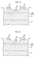
- FIG. 12 shows HFET or HEMT as the constructional example 3.
- FIG. 13 shows HFET or HEMT as the constructional example 4.
- the nitride based compound semiconductor layer 112 except an active area is electrically used as an inactivity isolation region.
- the active area is composed of the source finger electrode 120, the 2DEG layer 116 directly under the gate finger electrode 124 and the drain finger electrode 122, and the 2DEG layer 116 between the source finger electrode 120 and the gate finger electrode 124 and between the drain finger electrode 122 and the gate finger electrode 124.
- ion species nitrogen (N), argon (Ar), etc. are applicable, for example.
- the amount of dosage with the ion implantation is about 1x10 14 (ions/cm 2 ), for example, and accelerating energy is about 100 keV to 200 keV, for example.
- an insulating layer for passivation (not shown) is formed.
- the insulating layer it can be formed of a nitride film, an alumina (Al 2 O 3 ) film, an oxide film (SiO 2 ), an oxynitriding film (SiON), etc. deposited by a Plasma Enhanced Chemical Vapor Deposition (PECVD) method, for example.
- PECVD Plasma Enhanced Chemical Vapor Deposition
- the source finger electrode 120 and the drain finger electrode 122 are formed of Ti/Al etc., for example.
- the gate finger electrode 124 can be formed, for example of Ni/Au etc.
- the pattern length of the longitudinal direction of the gate finger electrode 124, the source finger electrode 120, and the drain finger electrode 122 is set up to be short as the operating frequency becomes higher such as the microwave/millimeter wave/submillimeter wave.
- the pattern length is about 25 ⁇ m to 50 ⁇ m.
- the width of the source finger electrode 120 is about 40 ⁇ m, for example, and the width of the source terminal electrode S11, S12, S21, S22, ..., S101, and S102 is about 100 ⁇ m, for example.
- the formation width of the VIA holes SC11, SC12, SC21, SC22, ..., SC101, and SC102 is about 10 ⁇ m to about 40 ⁇ m, for example.
- FIG. 14A A schematic bird's-eye view configuration of a package for mounting a semiconductor device 1 a according to a modified example of the embodiment, and a metal cap 10 is expressed as shown in FIG. 14A .
- a metal seal ring 14a is expressed as shown in FIG. 14B .
- a metal wall 16 is expressed as shown in FIG. 14C .
- a conductive base plate 200, and an input feed through 19a, an output feed through 19b and a feed through 39b utilized for capacitor disposed on an input side insulating layer 20a, an output side insulating layer 20b and an insulating layer 40b utilized for capacitor terminal, and each upper layer feed throughs 22 disposed on the input side insulating layer 20a, the output side insulating layer 20b, and the insulating layer 40b utilized for capacitor terminal are expressed as shown in FIG. 14D .
- a schematic plane constitution of the semiconductor device 1 according to the modified example of the embodiment is expressed as shown in FIG. 15 .
- the high frequency output terminal 21 b and the smoothing capacitor terminal 41 b are disposed so as to adjoin each other.
- the high frequency output terminal 21 b and the smoothing capacitor terminal 41 b are disposed at each side which is mutually adjoining in a quadrilateral. Since other configurations are the same as that of the semiconductor device 1 according to the embodiment, the duplicating explanation is omitted.
- the feed through 39b utilized for capacitor can be formed near by the semiconductor chip 24.
- the length of the bonding wire BW1 for connecting smoothing capacitor can be formed shorter than that of the first embodiment.
- the semiconductor device since it is connected without via the output matching circuit, it can be provide the semiconductor device which can smooth the voltage of the end face of drain of the high frequency semiconductor chip even when the difference frequency ⁇ f is several hundreds of MHz, and can be applied to the high frequency of the microwave/millimeter wave/submillimeter wave band.
- the high frequency semiconductor chip mounted in the semiconductor device it needless to say that not only the FET and HEMT but also amplifying elements, such as a Laterally Diffused Metal-Oxide-Semiconductor Field Effect Transistor (LDMOS) and a Hetero-junction Bipolar Transistor (HBT), and a Micro Electro Mechanical Systems (MEMS) element, etc. are applicable.
- LDMOS Laterally Diffused Metal-Oxide-Semiconductor Field Effect Transistor
- HBT Hetero-junction Bipolar Transistor
- MEMS Micro Electro Mechanical Systems
Landscapes
- Junction Field-Effect Transistors (AREA)
- Microwave Amplifiers (AREA)
- Amplifiers (AREA)
Abstract


Description
- Embodiments described herein generally relate to a semiconductor device.
- Conventionally, a resin-sealed type and a sealed and airtight type are known as a package utilized for a semiconductor element.
- The resin-sealed type semiconductor device has a structure which embedded directly the semiconductor element mounted in a leadframe in the resin by using a transfer mold etc., and is widely used by the advantage, such as low cost, being suitable for mass production, and a miniaturization being possible.
- The sealed and airtight type semiconductor device has a structure which performed in hollow airtight maintenance of the semiconductor element mounted on a base substance composed of conductive materials, such as copper. Although the cost is higher compared with the resin-sealed type semiconductor device, the sealed and airtight type semiconductor device is used when high reliability is required because of excellent in airtightness.
- In the sealed and airtight type package, it is known about an example of package mounting a semiconductor element directly on the heat radiation body composed of metal, and including input/output terminal units having convex feed through structure.
- When two frequencies are inputted into one high frequency amplifier, the difference frequency component occurs. When the difference frequency is several MHz, the voltage of output terminal and the voltage of chip end face are smoothed by connecting a capacitor which is not less than 100 micro F near an RF output terminal.
- However, when the difference frequency is several hundreds of MHz, the capacitor connected near the RF output terminal cannot smooth the voltage of the chip end face, since a matching circuit intervenes between the chip end face and the capacitor.
-
-
FIG. 1A shows a schematic bird's-eye view configuration of a package for mounting a semiconductor device according to an embodiment, and is a schematic configuration diagram of a metal cap. -
FIG. 1B shows a schematic bird's-eye view configuration of the package for mounting the semiconductor device according to the embodiment, and is a schematic configuration diagram of a metal seal ring. -
FIG. 1C shows a schematic bird's-eye view configuration of the package for mounting the semiconductor device according to the embodiment, and is a schematic configuration diagram of a metal wall. -
FIG. 1D shows a schematic bird's-eye view configuration of the package for mounting the semiconductor device according to the embodiment, and is a schematic configuration diagram of a conductive base plate, an insulating layer, a feed through disposed on the insulating layer, and an upper layer feed through disposed on the insulating layer. -
FIG. 2 is a schematic plane constitution diagram of the semiconductor device according to the embodiment. -
FIG. 3 is a schematic cross-sectional configuration of the semiconductor device according to the embodiment, and a schematic cross-sectional configuration diagram taken in the line 1-1 ofFIG. 2 . -
FIG. 4 is a schematic cross-sectional configuration of the semiconductor device according to the embodiment, and is a schematic cross-sectional configuration diagram taken in the line II-II ofFIG. 2 . -
FIG. 5 is a schematic cross-sectional configuration of the semiconductor device according to the embodiment, and is a schematic cross-sectional configuration diagram taken in the line III-III ofFIG. 2 . -
FIG. 6 is a schematic circuit configuration diagram of the semiconductor device according to the embodiment. -
FIG. 7 shows a simulation result showing the relationship between a ripple voltage ΔV applying a current amplitude IPK as a parameter, and a bypass reservoir capacitor CBR, in the semiconductor device according to the embodiment. -
FIG. 8 shows a simulation result showing the relationship of the ripple voltage ΔV applying difference frequency f as a parameter, and the bypass reservoir capacitor CBR, in the semiconductor device according to the embodiment. -
FIG. 9A is an enlarged drawing of schematic planar pattern configuration of a high frequency semiconductor chip, in the semiconductor device according to the embodiment. -
FIG. 9B is an enlarged drawing of a part J ofFIG. 9A . -
FIG. 10 is a constructional example 1 of the high frequency semiconductor chip applied to the semiconductor device according to the embodiment, and is a schematic cross-sectional configuration diagram taken in the line IV-IV ofFIG. 9B . -
FIG. 11 is a constructional example 2 of the high frequency semiconductor chip applied to the semiconductor device according to the embodiment, and is a schematic cross-sectional configuration diagram taken in the line IV-IV ofFIG. 9B . -
FIG. 12 is a constructional example 3 of the high frequency semiconductor chip applied to the semiconductor device according to the embodiment, and is a schematic cross-sectional configuration diagram taken in the line IV-IV ofFIG. 9B . -
FIG. 13 is a constructional example 4 of the high frequency semiconductor chip applied to the semiconductor device according to the embodiment, and is a schematic cross-sectional configuration diagram taken in the line IV-IV ofFIG. 9B . -
FIG. 14A shows a schematic bird's-eye view configuration of a package for mounting a semiconductor device according to a modified example of the embodiment, and is a schematic configuration diagram showing a metal cap. -
FIG. 14B shows a schematic bird's-eye view configuration of the package for mounting the semiconductor device according to the modified example of the embodiment, and is a schematic configuration diagram showing a metal seal ring. -
FIG. 14C shows a schematic bird's-eye view configuration of the package for mounting the semiconductor device according to the modified example of the embodiment, and is a schematic configuration diagram showing a metal wall. -
FIG. 14D is a schematic bird's-eye view configuration of the package for mounting the semiconductor device according to the modified example of the embodiment, and is a schematic configuration diagram of a conductive base plate, an insulating layer, a feed through disposed on the insulating layer, and an upper layer feed through disposed on the insulating layer. -
FIG. 15 is a schematic plane constitution diagram of the semiconductor device according to the modified example of the embodiment. - Next, embodiments will be described with reference to drawings.
- According to one embodiment, a semiconductor device includes a high frequency semiconductor chip, an input matching circuit, an output matching circuit, a high frequency input terminal, a high frequency output terminal, and a smoothing capacitor terminal. The input matching circuit is disposed at the input side of the high frequency semiconductor chip. The output matching circuit is disposed at the output side of the high frequency semiconductor chip. The high frequency input terminal is connected to the input matching circuit. The high frequency output terminal is connected to the output matching circuit. The smoothing capacitor terminal is connected to the high frequency semiconductor chip. The high frequency semiconductor chip, the input matching circuit, and the output matching circuit are housed by one package.
-
FIG. 1 shows a schematic bird's-eye view configuration of a package for mounting asemiconductor device 1 according to an embodiment. Ametal cap 10 is expressed as shown inFIG. 1A . Ametal seal ring 14a is expressed as shown inFIG. 1B , ametal wall 16 is expressed as shown inFIG. 1C . Aconductive base plate 200, and an input feed through 19a, an output feed through 19b and a feed through 39b utilized for capacitor disposed on an inputside insulating layer 20a, an outputside insulating layer 20b and an insulatinglayer 40b utilized for capacitor terminal are expressed as shown inFIG. 1D . - As shown in
FIG. 1A to FIG. 1D , the package for mounting thesemiconductor device 1 according to the embodiment includes: ametal cap 10; ametal seal ring 14a; ametallic wall 16; aconductive base plate 200; an inputside insulating layer 20a, an outputside insulating layer 20b and an insulatinglayer 40b utilized for capacitor terminal disposed on theconductive base plate 200; an input feed through 19a disposed on the inputside insulating layer 20a; an output feed through 19b disposed on the outputside insulating layer 20b; a feed through 39b utilized for capacitor disposed on the insulatinglayer 40b utilized for capacitor terminal; and upperlayer feed throughs 22 disposed on the inputside insulating layer 20a, the outputside insulating layer 20b and the insulatinglayer 40b utilized for capacitor terminal. - The
conductive base plate 200 is formed of conductive metals, such as copper and a copper molybdenum alloy, for example. Furthermore, electroplated conductors, such as Au, Ni, Ag, an Ag-Pt alloy and an Ag-Pd alloy, may be formed on the surface of theconductive base plate 200, for example. Also, layered structure, such as Cu/Mo/Mo substrate, may be used for theconductive base plate 200. - As a material of the
metallic wall 16, it is formed of conductive metals, such as aluminum, molybdenum, and a copper molybdenum alloy, for example. A soldering metal layer (not shown) for soldering is formed on the top surface of themetallic wall 16 via themetal seal ring 14a. The solder metal layer can be formed of a gold germanium alloy, a gold tin alloy, etc., for example. - Moreover, the
metallic wall 16 is disposed on theconductive base plate 200 via a conductive adhesive material. In addition, themetal wall 16 is disposed on the convex upper layer feed through 22, in the feed-through portion (refer toFIG. 1 andFIG. 3 ). Each of the convex upperlayer feed throughs 22 is disposed on the inputside insulating layer 20a and the outputside insulating layer 20b and the insulatinglayer 40b utilized for capacitor terminal, respectively, and is formed by an insulating layer. In this case, the inputside insulating layer 20a, the outputside insulating layer 20b and the insulatinglayer 40b utilized for capacitor terminal are equivalent to a lower layer feed through. The insulating adhesive material can be formed of an epoxy resin, glass, etc., for example, and the conductive adhesive material can be formed of a gold germanium alloy, a gold tin alloy, etc., for example. - The
metal cap 10 has a flat plate shape as shown inFIG. 1A . - The
metal cap 10 is disposed on themetallic wall 16 via themetal seal ring 14a. - The package for mounting the
semiconductor device 1 according to the embodiment has a high frequency characteristics of not less than 2 GHz. Accordingly, the package according to the first embodiment is applicable as a package for devices and component parts having high frequency (that is, frequency over 2 GHz). - A schematic planar pattern configuration of the
semiconductor device 1 according to the embodiment is expressed as shown inFIG. 2 , a schematic cross-section structure taken in the line I-I ofFIG. 2 is expressed as shown inFIG. 3 , a schematic cross-section structure taken in the line II-II ofFIG. 2 is expressed as shown inFIG. 4 , and a schematic cross-section structure taken in the line III-III ofFIG. 2 is expressed as shown inFIG. 5 . - As shown in
FIG. 2 to FIG. 5 , thesemiconductor device 1 according to the embodiment includes: a highfrequency semiconductor chip 24; aninput matching circuit 17 disposed at the input side of the highfrequency semiconductor chip 24; anoutput matching circuit 18 disposed at the output side of the highfrequency semiconductor chip 24; a highfrequency input terminal 21 a connected to theinput matching circuit 17; a highfrequency output terminal 21 b connected to theoutput matching circuit 18; and a smoothingcapacitor terminal 41 b connected to the highfrequency semiconductor chip 24. In this case, the highfrequency semiconductor chip 24, theinput matching circuit 17 and theoutput matching circuit 18 are housed by one package. - As shown in
FIG. 2 andFIG. 4 , thesemiconductor device 1 according to the embodiment includes a bypass reservoir capacitor (smoothing capacitor) CBR connected between the smoothingcapacitor terminal 41 b and the ground potential (earth potential). The smoothing capacitor CBR has a value more than CBR= IPK×(1/2πΔf)/ΔV
where CBR is a value of the smoothing capacitor CBR, IPK is a value of current amplitude, ΔV is a value of an allowable ripple voltage, and Δf is a value of difference frequency. - The
semiconductor device 1 according to the embodiment includes the feed through 39b utilized for capacitor connected to the highfrequency semiconductor chip 24, as shown inFIG. 2 andFIG. 3 . In this case, the smoothingcapacitor terminal 41 b is connected to the drain terminal electrode D of the highfrequency semiconductor chip 24 via the feed through 39b utilized for capacitor. - Also, as shown in
FIG. 2 andFIG. 4 , thesemiconductor device 1 according to the embodiment includes a bonding wire BW1 for connecting smoothing capacitor which connects between a drain terminal electrode D of the highfrequency semiconductor chip 24, and the feed through 39b utilized for capacitor. - Also, as shown in
FIG. 2 andFIG. 3 , thesemiconductor device 1 according to the embodiment includes the input feed through 19a connected to theinput matching circuit 17, and the highfrequency input terminal 21 a is connected to a gate terminal electrode G of the highfrequency semiconductor chip 24 via the input feed through 19a. - Also, as shown in
FIG. 2 andFIG. 3 , thesemiconductor device 1 according to the embodiment includes the output feed through 19b connected to theoutput matching circuit 18, and the highfrequency output terminal 21 b is connected to the drain terminal electrode D of the highfrequency semiconductor chip 24 via the output feed through 19b. - Also, as shown in
FIG. 2 , the highfrequency output terminal 21 b and the smoothingcapacitor terminal 41 b may be disposed to adjoin each other. - Also, as shown in
FIG. 2 to FIG. 5 , thesemiconductor device 1 according to the embodiment includes: the highfrequency semiconductor chip 24 disposed on theconductive base plate 200; aninput circuit substrate 26 disposed on theconductive base plate 200 at the input side of the highfrequency semiconductor chip 24; and anoutput circuit substrate 28 disposed on theconductive base plate 200 at the output side of the highfrequency semiconductor chip 24. - The
input matching circuit 17 is disposed on theinput circuit substrate 26. Moreover, theoutput matching circuit 18 is disposed on theoutput circuit substrate 28. - The
input matching circuit 17 is connected to the gate terminal electrode G of the highfrequency semiconductor chip 24 via thebonding wire 12, and theoutput matching circuit 18 is connected to the drain terminal electrode D of the highfrequency semiconductor chip 24 via thebonding wire 14. - The high
frequency input terminal 21a is connected to the input feed through 19a, and the highfrequency output terminal 21 b is connected to the output feed through 19b. - The high
frequency input terminal 21a is connected to the gate terminal electrode G of the highfrequency semiconductor chip 24 via the input feed through 19a, thebonding wire 11 and theinput matching circuit 17. - As shown in
FIG. 6 , a schematic circuit configuration of thesemiconductor device 1 according to the embodiment includes: the highfrequency semiconductor chip 24; theinput matching circuit 17 disposed at the input side of the highfrequency semiconductor chip 24; theoutput matching circuit 18 disposed at the output side of the highfrequency semiconductor chip 24; the input feed through 19a connected to theinput matching circuit 17; the highfrequency input terminal 21a connected to the input feed through 19a; the output feed through 19b connected to theoutput matching circuit 18; the highfrequency output terminal 21 b connected to the output feed through 99b; acapacitor connection circuit 80 disposed at the output side of the highfrequency semiconductor chip 24; and the smoothingcapacitor terminal 41 b connected to thecapacitor connection circuit 80. In this case, the highfrequency semiconductor chip 24, theinput matching circuit 17 and theoutput matching circuit 18 are housed by one package surrounded by themetal wall 16. - The
capacitor connection circuit 80 includes a bonding wire BW1 for connecting smoothing capacitor which connects between the drain terminal electrode D of the highfrequency semiconductor chip 24 and the feed through 39b utilized for capacitor. - Also, as shown in
FIG. 6 , the electrode of one side of the smoothing capacitor CBR is connected to the smoothingcapacitor terminal 41 b via a bonding wire for connecting smoothing capacitor BW2, and the electrode of another side of the smoothing capacitor CBR is connected to the ground potential via a bonding wire for connecting smoothing capacitor BW3. - As shown in
FIG. 6 , thesemiconductor device 1 according to the embodiment includes the smoothingcapacitor terminal 41 b, and the smoothingcapacitor terminal 41 b is connected with the drain terminal electrode D of the highfrequency semiconductor chip 24 via the feed through 39b utilized for capacitor and the bonding wire BW1 for connecting smoothing capacitor. In the above-mentioned connection, since it is connected without via theoutput matching circuit 18, even when the difference frequency Δf is several hundreds of MHz, the voltage of the drain terminal electrode D of the highfrequency semiconductor chip 24 is smoothed. -
FIG. 7 shows a simulation result showing the relationship between the ripple voltage ΔV applying a current amplitude IPK as a parameter, and the bypass reservoir capacitor (smoothing capacitor) CBR, in thesemiconductor device 1 according to the embodiment.FIG. 7 shows an example that the difference frequency Δf is equal to 5 MHz. - As shown in
FIG. 7 , in order to reduce the ripple voltage ΔV to not more than 0.1 V, for example, when the difference frequency Δf is 50 MHz and the current amplitude IPK is 0.3A, the value of not less than 0.1 µF is needed for the bypass reservoir capacitor CBR. Similarly, when the difference frequency Δf is 50 MHz and the current amplitude IPK is 1.0A, the value of not less than 0.3 µF is needed for the bypass reservoir capacitor CBR. Similarly, when the difference frequency Δf is 50 MHz and the current amplitude IPK is 3.0A, the value of not less than 1.0 µF is needed for the bypass reservoir capacitor CBR. - On the other hand,
FIG. 8 shows a simulation result showing the relationship between the ripple voltage ΔV applying the difference frequency Δf as a parameter, and the bypass reservoir capacitor (smoothing capacitor) CBR. - As shown in
FIG. 8 , in order to reduce the ripple voltage ΔV to not more than 0.1 V, for example, where the current amplitude IPK is 3A and the difference frequency Δf is 1 MHz the value of not less than 5 µF is needed for the bypass reservoir capacitor CBR. Similarly, where the current amplitude IPK is 3A and the difference frequency Δf is 5 MHz, the value of not less than 1 µF is needed for the bypass reservoir capacitor CBR. Similarly, where the current amplitude IPK is 3A and the difference frequency Δf is 50 MHz, the value of not less than 0.1 µF is needed for the bypass reservoir capacitor CBR. - The
semiconductor device 1 according to the embodiment connects between the end face of drain terminal electrode D of the highfrequency semiconductor chip 24 and the bypass reservoir capacitor (smoothing capacitor) CBR at the shortest, and thereby the inductance between the end face of drain terminal electrode D of the highfrequency semiconductor chip 24 and the bypass reservoir capacitor CBR can be reduced to the minimum. - For example, in the case of 6 GHz band 80 W class GaAsMESFET (for example, TIM5964-80SL manufactured by Toshiba Corporation, Japan), when the difference frequency Δf is 5 MHz, the value of the current amplitude IPK at the time of operation in -25 dBc is about 3A, and the value of the bypass reservoir capacitor CBR needed in order to supply the amount of charge within the cycle of 5 MHz and for the ripple voltage ΔV to be within 0.1 V can be expressed by CBR = Q/ΔV
where Q = IPKxintegral(0 to T/2)sinωtdt = IPKxintegral(0 to Π/ω)sinωtdt, and therefore, the value of Q is 3x(1/2Πf) = about 1x10⁻⁷ (C), and CBR is 1 µF derived from the ripple voltage ΔV is 0.1 V. - In the case of measuring of third order intermodulation distortion IM3, when two frequencies are inputted into the one
semiconductor device 1, the difference frequency component occurs. Here, when two input signals whose frequencies are nearly equal (frequencies f1 and f2; where f1-f2 = several tens of MHz) is supplied to thesemiconductor device 1, although signals having frequencies (2f2-f1) and (2f1-f2) are output from thesemiconductor device 1 according to the nonlinear characteristics of the device, the third order intermodulation distortion IM3 has notated the signal level by the ratio to the signal level of the fundamental wave (f1 or f2). - In the basic measuring method of third order intermodulation distortion IM3, two fundamental wave signals are mixed and used for the
semiconductor device 1 as an input signal. The third order intermodulation distortion IM3 occurred with thesemiconductor device 1 is measured by a spectrum analyzer. - When the difference frequency Δf is several MHz, the output voltage and the voltage of the end face of drain of the high
frequency semiconductor chip 24 are smoothed by connecting a capacitor having electrostatic capacity of not less than 100 µF near the RF output terminal. - However, when a certain impedance exists between the bias power supply source and the end face of drain of the high
frequency semiconductor chip 24, the voltage which appears in the end face of drain .of the highfrequency semiconductor chip 24 is modulated, thereby causing a negative effect on the amplification characteristics of thesemiconductor device 1. For example, between the bias power supply source and the end face of drain of the highfrequency semiconductor chip 24, a reactance (inductance L) exists corresponding to the distance. The modulated voltage amplitude (ripple voltage ΔV) is expressed by 2πf×L×l where the alternating current of the frequency component f is I. - Accordingly, the effective bias power supply source is close to the high
frequency semiconductor chip 24 by disposing the bypass reservoir capacitor CBR near the highfrequency semiconductor chip 24, and therefore the reactance between the bias power supply source and the end face of drain of the highfrequency semiconductor chip 24 can be kept small. In this case, the voltage of the end face of drain of the highfrequency semiconductor chip 24 is the voltage of the end face of drain terminal electrode D of the highfrequency semiconductor chip 24. - Since the ripple voltage ΔV is expressed by ΔV=2πf×L×l, L=ΔV/(2πf×l) is satisfied. Therefore, when l=3 A and f=5 MHz, what is necessary is just to satisfy L<0.1/(2π×5×10-6×3), and to connect the bypass reservoir capacitor CBR within the distance from which the value of L is about 1 mH, in order to reduce the voltage amplitude (the ripple voltage ΔV) to not more than 0.1 V.
- Also, when l=3 A and f=100 MHz, what is necessary is just to satisfy L<0.1/(2π×100×10-6×3), and to connect the bypass reservoir capacitor CBR within the distance from which the value of L is about 50 µH, in order to reduce the voltage amplitude (the ripple voltage ΔV) to not more than 0.1V.
- Moreover, the reason for connecting the drain terminal electrode D of the high
frequency semiconductor chip 24 and the feed through 39b utilized for capacitor via the bonding wire BW1 for connecting smoothing capacitor is that connecting by the wire bonding is the optimum choice since the effective electric length is short. - According to the embodiment, since it is connected without via the output matching circuit, it can be provide the semiconductor device which can smooth the voltage of the end face of drain of the high frequency semiconductor chip even when the difference frequency Δf is several hundreds of MHz, and can be applied to the high frequency of the microwave/millimeter wave/submillimeter wave band.
- An enlarged drawing of a schematic planar pattern configuration of the high
frequency semiconductor chip 24 applied to thesemiconductor device 1 according to the embodiment is expressed as shown inFIG. 9A , and an enlarged drawing of a part J ofFIG. 9A is expressed as shown inFIG. 9B . Also, configuration examples 1-4 of the highfrequency semiconductor chip 24 applied to thesemiconductor device 1 according to the embodiment, and schematic cross section configuration examples 1-4 taken in the line IV-IV ofFIG. 9B are expressed as shown inFIG. 10 to FIG. 13 , respectively. - In the high frequency semiconductor chip 24 applied to the semiconductor device 1 according to the embodiment, as shown in
FIG. 9 to FIG. 13 , a plurality of FET cells FET 1 to FET 10 include: a semi-insulating substrate 110; a gate finger electrode 124, a source finger electrode 120, and a drain finger electrode 122 which are disposed on a first surface of the semi-insulating substrate 110, and have a plurality of fingers, respectively; a plurality of gate terminal electrodes G1, G2, ..., G10, a plurality of source terminal electrodes S11, S12, S21, S22, ..., S101, and S102 and the drain terminal electrodes D1, D2, ..., D10 which are disposed on the first surface of the semi-insulating substrate 110, and ties a plurality of fingers, respectively every the gate finger electrode 124, the source finger electrode 120, and the drain finger electrode 122; VIA holes SC11, SC12, SC21, SC22, ..., SC101, and SC102 disposed at the lower part of the source terminal electrodes S11, S12, S21, S22, ..., S101, and S102; and a ground electrode (not shown) which is disposed on a second surface of the opposite side of a first surface of the semi-insulating substrate 110, and is connected via the VIA holes SC11, SC12, SC21, SC22, ..., SC101, and SC102 to the source terminal electrodes S11, S12, S21, S22, ..., S101, and S102. - The
bonding wire 12 is connected to the gate terminal electrodes G1, G2, ..., G10, and thebonding wire 14 is connected to the drain terminal electrodes D1, D2, ..., D10. - The source terminal electrodes S11, S12, S21, S22, ..., S101, and S102 are connected to the ground electrode (not shown), via the barrier metal layers (not shown) formed in the internal wall of the VIA holes SC11, SC12, SC21, SC22, ..., SC101 and SC102, and via the filling metal layers formed on the barrier metal layers and filled up with the VIA holes
- The
semi-insulating substrate 110 is either of a GaAs substrate, an SiC substrate, a GaN substrate, a substrate in which a GaN epitaxial layer is formed on the SiC substrate, a substrate which a heterojunction epitaxial layer composed of GaN/AlGaN is formed on the SiC substrate, a sapphire substrate or a diamond substrate. - As shown in
FIG. 10 , a configuration example 1 of an FET cell of the highfrequency semiconductor chip 24 applied to the semiconductor device according to the embodiment, as a schematic cross-sectional configuration taken in the line IV-IV ofFIG. 9B , includes: asemi-insulating substrate 110; a nitride basedcompound semiconductor layer 112 disposed on thesemi-insulating substrate 110; an aluminum gallium nitride layer (AlxGa1-xN) (where 0.1<=x<=1) 118 disposed on the nitride basedcompound semiconductor layer 112; and asource finger electrode 120, agate finger electrode 124, and adrain finger electrode 122 which are disposed on the aluminum gallium nitride layer (AlxGa1-xN) (where 0.1<=x<=1) 118. A two dimensional electron gas (2DEG)layer 116 is formed in the interface between the nitride basedcompound semiconductor layer 112 and the aluminum gallium nitride layer (AlxGa1-xN) (where 0.1 <=x<=1) 118.FIG. 10 shows a Hetero-junction Field Effect Transistor (HFET) or a High Electron Mobility Transistor (HEMT) as the constructional example 1. - As shown in
FIG. 11 , a constructional example 2 of an FET cell of the highfrequency semiconductor chip 24 applied to the semiconductor device according to the embodiment, as a schematic cross-sectional configuration taken in the line IV-IV ofFIG. 9B , includes: asemi-insulating substrate 110; a nitride basedcompound semiconductor layer 112 disposed on thesemi-insulating substrate 110; asource region 126 and adrain region 128 which are disposed on the nitride basedcompound semiconductor layer 112; and asource finger electrode 120 disposed on thesource region 126, agate finger electrode 124 disposed on the nitride basedcompound semiconductor layer 112, and adrain finger electrode 122 disposed on thedrain region 128. Schottky contact is formed in the interface between the nitride basedcompound semiconductor layer 112 and thegate finger electrode 124.FIG. 11 shows a Metal Semiconductor Field Effect Transistor (MESFET) as the constructional example 2. - As shown in
FIG. 12 , a constructional example 3 of an FET cell of the highfrequency semiconductor chip 24 applied to the semiconductor device according to the embodiment, as a schematic cross-sectional configuration taken in the line IV-IV ofFIG. 9B , includes: asemi-insulating substrate 110; a nitride basedcompound semiconductor layer 112 disposed on thesemi-insulating substrate 110; an aluminum gallium nitride layer (AlxGa1-xN) (where 0.1<=x<=1) 118 disposed on the nitride basedcompound semiconductor layer 112; asource finger electrode 120 and adrain finger electrode 122 which are disposed on the aluminum gallium nitride layer (AlxGa1-xN) (where 0.1<=x<=1) 118; and agate finger electrode 124 disposed at a recessed part on the aluminum gallium nitride layer (AlxGa1-xN) (where 0.1<=x<=1) 118. The2DEG layer 116 is formed in the interface between the nitride basedcompound semiconductor layer 112 and the aluminum gallium nitride layer (AIxGa1-xN) (where 0.1<=x<=1 ) 118.FIG. 12 shows HFET or HEMT as the constructional example 3. - As shown in
FIG. 13 , a constructional example 4 of an FET cell of the highfrequency semiconductor chip 24 applied to the semiconductor device according to the embodiment, as a schematic cross-sectional configuration taken in the line IV-IV ofFIG. 9B , includes: asemi-insulating substrate 110; a nitride basedcompound semiconductor layer 112 disposed on thesemi-insulating substrate 110; an aluminum gallium nitride layer (AlxGa1-xN) (where 0.1<=x<=1) 118 disposed on the nitride basedcompound semiconductor layer 112; asource finger electrode 120 and adrain finger electrode 122 which are disposed on the aluminum gallium nitride layer (AlxGa1-xN) (where 0.1<=x<=1) 118; and agate finger electrode 124 disposed at a two-step recessed part on the aluminum gallium nitride layer (AlxGa1-xN) (where 0.1<=x<=1) 118. The2DEG layer 116 is formed in the interface between the nitride basedcompound semiconductor layer 112 and the aluminum gallium nitride layer (AlxGa1-xN) (where 0.1<=x<=1) 118.FIG. 13 shows HFET or HEMT as the constructional example 4. - Moreover, in the above-mentioned constructional examples 1-4, the nitride based
compound semiconductor layer 112 except an active area is electrically used as an inactivity isolation region.Here, the active area is composed of thesource finger electrode 120, the2DEG layer 116 directly under thegate finger electrode 124 and thedrain finger electrode 122, and the2DEG layer 116 between thesource finger electrode 120 and thegate finger electrode 124 and between thedrain finger electrode 122 and thegate finger electrode 124. - As another fabrication method of the isolation region, it can also form by ion implantation to a part of depth direction of the aluminum gallium nitride layer (AlxGa1-xN) (where 0.1<=x<=1) 18 and the nitride based
compound semiconductor layer 112. As ion species, nitrogen (N), argon (Ar), etc. are applicable, for example. Moreover, the amount of dosage with the ion implantation is about 1x10¹⁴ (ions/cm2), for example, and accelerating energy is about 100 keV to 200 keV, for example. - On the isolation region and the device surface, an insulating layer for passivation (not shown) is formed. As the insulating layer, it can be formed of a nitride film, an alumina (Al2O3) film, an oxide film (SiO2), an oxynitriding film (SiON), etc. deposited by a Plasma Enhanced Chemical Vapor Deposition (PECVD) method, for example.
- The
source finger electrode 120 and thedrain finger electrode 122 are formed of Ti/Al etc., for example. Thegate finger electrode 124 can be formed, for example of Ni/Au etc. - In addition, in the high
frequency semiconductor chip 24 applied to the semiconductor device according to the embodiment, the pattern length of the longitudinal direction of thegate finger electrode 124, thesource finger electrode 120, and thedrain finger electrode 122 is set up to be short as the operating frequency becomes higher such as the microwave/millimeter wave/submillimeter wave. For example, in the millimeter wave band, the pattern length is about 25 µm to 50 µm. - Also, the width of the
source finger electrode 120 is about 40 µm, for example, and the width of the source terminal electrode S11, S12, S21, S22, ..., S101, and S102 is about 100 µm, for example. Yet also, the formation width of the VIA holes SC11, SC12, SC21, SC22, ..., SC101, and SC102 is about 10 µm to about 40 µm, for example. - A schematic bird's-eye view configuration of a package for mounting a
semiconductor device 1 a according to a modified example of the embodiment, and ametal cap 10 is expressed as shown inFIG. 14A . Ametal seal ring 14a is expressed as shown inFIG. 14B . Ametal wall 16 is expressed as shown inFIG. 14C . Aconductive base plate 200, and an input feed through 19a, an output feed through 19b and a feed through 39b utilized for capacitor disposed on an inputside insulating layer 20a, an outputside insulating layer 20b and an insulatinglayer 40b utilized for capacitor terminal, and each upperlayer feed throughs 22 disposed on the inputside insulating layer 20a, the outputside insulating layer 20b, and the insulatinglayer 40b utilized for capacitor terminal are expressed as shown inFIG. 14D . - A schematic plane constitution of the
semiconductor device 1 according to the modified example of the embodiment is expressed as shown inFIG. 15 . - In the
semiconductor device 1 according to the embodiment, as shown inFIG. 2 , the highfrequency output terminal 21 b and the smoothingcapacitor terminal 41 b are disposed so as to adjoin each other. On the other hand, in thesemiconductor device 1 a according to the modified example of the embodiment, as shown inFIG. 15 , the highfrequency output terminal 21 b and the smoothingcapacitor terminal 41 b are disposed at each side which is mutually adjoining in a quadrilateral. Since other configurations are the same as that of thesemiconductor device 1 according to the embodiment, the duplicating explanation is omitted. - According to the modified example of the embodiment, the feed through 39b utilized for capacitor can be formed near by the
semiconductor chip 24. For that reason, according to the modified example of the embodiment, the length of the bonding wire BW1 for connecting smoothing capacitor can be formed shorter than that of the first embodiment. - According to the embodiment and its modified example, since it is connected without via the output matching circuit, it can be provide the semiconductor device which can smooth the voltage of the end face of drain of the high frequency semiconductor chip even when the difference frequency Δf is several hundreds of MHz, and can be applied to the high frequency of the microwave/millimeter wave/submillimeter wave band.
- While certain embodiment and its modified example have been described, these embodiment and its modified example have been presented by way of examples only, and are not intended to limit the scope of the inventions. Indeed, the novel methods and systems described herein may be embodied in a variety of other forms; furthermore, various omissions, substitutions and changes in the form of the methods and systems described herein may be made without departing from the spirit of the inventions. The accompanying claims and their equivalents are intended to cover such forms or modifications as would fall within the scope and spirit of the inventions.
- In addition, as the high frequency semiconductor chip mounted in the semiconductor device according to the embodiments, it needless to say that not only the FET and HEMT but also amplifying elements, such as a Laterally Diffused Metal-Oxide-Semiconductor Field Effect Transistor (LDMOS) and a Hetero-junction Bipolar Transistor (HBT), and a Micro Electro Mechanical Systems (MEMS) element, etc. are applicable.
- Thus, it includes various embodiments etc. which have not been described in this specification.
Claims (10)
- A semiconductor device comprising:a high frequency semiconductor chip;an input matching circuit disposed at an input side of the high frequency semiconductor chip;an output matching circuit disposed at an output side of the high frequency semiconductor chip;a high frequency input terminal connected to the input matching circuit;a high frequency output terminal connected to the output matching circuit; anda smoothing capacitor terminal connected to the high frequency semiconductor chip, whereinthe high frequency semiconductor chip, the input matching circuit and the output matching circuit are housed by one package.
- The semiconductor device according to claim 1 further comprising:a smoothing capacitor connected between the smoothing capacitor terminal and ground potential, whereinthe smoothing capacitor has a value more than CBR=lPK×(1/2πΔf)/ΔVwhere CBR is a value of the smoothing capacitor, IPK is a value of current amplitude, ΔV is a value of an allowable ripple voltage, and Δf is a value of difference frequency.
- The semiconductor device according to claim 1 further comprising:a feed through utilized for capacitor connected to the high frequency semiconductor chip, whereinthe smoothing capacitor terminal is connected to the drain terminal electrode of the high frequency semiconductor chip via the feed through utilized for capacitor.
- The semiconductor device according to claim 3 further comprising:a bonding wire for connecting smoothing capacitor connecting between the drain terminal electrode of the high frequency semiconductor chip, and the feed through utilized for capacitors.
- The semiconductor device according to claim 1 further comprising:an input feed through connected to the input matching circuit, whereinthe high frequency input terminal is connected to the gate terminal electrode of the high frequency semiconductor chip via the input feed through.
- The semiconductor device according to claim 1 further comprising:an output feed through connected to the output matching circuit, whereinthe high frequency output terminal is connected to the drain terminal electrode of the high frequency semiconductor chip via the output feed through.
- The semiconductor device according to any one of claim 1, 2, 3, 4, 5, or 6, wherein
the high frequency output terminal and the smoothing capacitor terminal are disposed to adjoin each other. - The semiconductor device according to any one of claim 1, 2, 3, 4, 5, or 6, wherein
the high frequency output terminal and the smoothing capacitor terminal are disposed at each side being mutually adjoining in a quadrilateral. - The semiconductor device according to claim 1, wherein
the high frequency semiconductor chip comprises:a semi-insulating substrate;a gate finger electrode, a source finger electrode, and a drain finger electrode configured to be disposed on a first surface of the semi-insulating substrate, and configured to have a plurality of fingers, respectively;a plurality of gate terminal electrodes, a plurality of source terminal electrodes, and a drain terminal electrode configured to be disposed on the first surface of the semi-insulating substrate, and configured to tie a plurality of fingers, respectively for every the gate finger electrode, the source finger electrode, and the drain finger electrode;a VIA hole configured to be disposed at a lower part of the source terminal electrode; anda ground electrode configured to be disposed on a second surface of the opposite side of the first surface of the semi-insulating substrate, and configured to be connected via the VIA hole for the source terminal electrode. - The semiconductor device according to claim 9, wherein
the semi-insulating substrate is one of a GaAs substrate, an SiC substrate, a GaN substrate, a substrate formed of a GaN epitaxial layer on the SiC substrate, a substrate formed of a heterojunction epitaxial layer composed of GaN/AlGaN on the SiC substrate, a sapphire substrate, or a diamond substrate.
Applications Claiming Priority (1)
| Application Number | Priority Date | Filing Date | Title |
|---|---|---|---|
| JP2010272916A JP5269864B2 (en) | 2010-12-07 | 2010-12-07 | Semiconductor device |
Publications (3)
| Publication Number | Publication Date |
|---|---|
| EP2463906A2 true EP2463906A2 (en) | 2012-06-13 |
| EP2463906A3 EP2463906A3 (en) | 2013-03-06 |
| EP2463906B1 EP2463906B1 (en) | 2021-11-24 |
Family
ID=45002549
Family Applications (1)
| Application Number | Title | Priority Date | Filing Date |
|---|---|---|---|
| EP11170565.3A Active EP2463906B1 (en) | 2010-12-07 | 2011-06-20 | Semiconductor device |
Country Status (3)
| Country | Link |
|---|---|
| US (1) | US8912647B2 (en) |
| EP (1) | EP2463906B1 (en) |
| JP (1) | JP5269864B2 (en) |
Families Citing this family (5)
| Publication number | Priority date | Publication date | Assignee | Title |
|---|---|---|---|---|
| JP5588419B2 (en) * | 2011-10-26 | 2014-09-10 | 株式会社東芝 | package |
| JP5983117B2 (en) * | 2012-07-11 | 2016-08-31 | 三菱電機株式会社 | Semiconductor device |
| WO2015046209A1 (en) * | 2013-09-27 | 2015-04-02 | 京セラ株式会社 | Lid body, package, and electronic apparatus |
| WO2018211643A1 (en) * | 2017-05-17 | 2018-11-22 | 三菱電機株式会社 | Amplifier |
| US20230075505A1 (en) * | 2021-09-03 | 2023-03-09 | Wolfspeed, Inc. | Metal pillar connection topologies for heterogeneous packaging |
Family Cites Families (23)
| Publication number | Priority date | Publication date | Assignee | Title |
|---|---|---|---|---|
| FR2538617B1 (en) | 1982-12-28 | 1986-02-28 | Thomson Csf | ENCAPSULATION BOX FOR POWER SEMICONDUCTOR WITH IMPROVED INPUT-OUTPUT ISOLATION |
| JPH0260205A (en) * | 1988-08-25 | 1990-02-28 | Matsushita Electric Ind Co Ltd | Microwave integrated circuit and its manufacturing method |
| JPH0269002A (en) | 1988-09-05 | 1990-03-08 | Fujitsu Ltd | Microwave and millimeter wave accumulating equipment |
| JPH05152876A (en) * | 1991-11-26 | 1993-06-18 | Toshiba Corp | Power limiting element |
| JP2864841B2 (en) * | 1992-02-04 | 1999-03-08 | 三菱電機株式会社 | High frequency high power transistor |
| US5422615A (en) * | 1992-09-14 | 1995-06-06 | Hitachi, Ltd. | High frequency circuit device |
| JPH07297609A (en) * | 1994-04-28 | 1995-11-10 | Nec Yamagata Ltd | Semiconductor device |
| JP3060981B2 (en) * | 1997-02-21 | 2000-07-10 | 日本電気株式会社 | Microwave amplifier |
| JP3336982B2 (en) * | 1998-12-16 | 2002-10-21 | 松下電器産業株式会社 | Semiconductor device and method of manufacturing the same |
| JP4163818B2 (en) * | 1999-07-07 | 2008-10-08 | 三菱電機株式会社 | Internally matched transistor |
| JP2001111364A (en) * | 1999-10-12 | 2001-04-20 | Nec Corp | Microwave amplifier |
| JP4322414B2 (en) * | 2000-09-19 | 2009-09-02 | 株式会社ルネサステクノロジ | Semiconductor device |
| JP2003068571A (en) * | 2001-08-27 | 2003-03-07 | Nec Corp | Variable capacitor and variable inductor and high-frequency circuit module provided with them |
| EP1472734A2 (en) * | 2002-01-24 | 2004-11-03 | Koninklijke Philips Electronics N.V. | Rf amplifier |
| US7087977B2 (en) * | 2002-09-27 | 2006-08-08 | Renesas Technology Corp. | Semiconductor device including multiple wiring layers and circuits operating in different frequency bands |
| JP4049112B2 (en) * | 2004-03-09 | 2008-02-20 | 株式会社日立製作所 | Electronic equipment |
| JP4519637B2 (en) | 2004-12-28 | 2010-08-04 | 株式会社東芝 | Semiconductor device |
| JP2007060616A (en) * | 2005-07-29 | 2007-03-08 | Mitsubishi Electric Corp | High frequency power amplifier |
| JP4575261B2 (en) | 2005-09-14 | 2010-11-04 | 株式会社東芝 | High frequency package |
| US7733187B2 (en) * | 2006-10-13 | 2010-06-08 | Panasonic Corporation | High frequency power amplifier |
| JP2008288769A (en) * | 2007-05-16 | 2008-11-27 | Panasonic Corp | High frequency circuit, semiconductor device, and high frequency power amplifier |
| WO2009128035A1 (en) * | 2008-04-15 | 2009-10-22 | Nxp B.V. | High frequency field-effect transistor |
| JP5434019B2 (en) * | 2008-09-03 | 2014-03-05 | 三菱電機株式会社 | Inspection jig |
-
2010
- 2010-12-07 JP JP2010272916A patent/JP5269864B2/en active Active
-
2011
- 2011-06-20 EP EP11170565.3A patent/EP2463906B1/en active Active
- 2011-06-20 US US13/164,217 patent/US8912647B2/en active Active
Non-Patent Citations (1)
| Title |
|---|
| None |
Also Published As
| Publication number | Publication date |
|---|---|
| EP2463906A3 (en) | 2013-03-06 |
| EP2463906B1 (en) | 2021-11-24 |
| JP2012124282A (en) | 2012-06-28 |
| US8912647B2 (en) | 2014-12-16 |
| JP5269864B2 (en) | 2013-08-21 |
| US20120138954A1 (en) | 2012-06-07 |
Similar Documents
| Publication | Publication Date | Title |
|---|---|---|
| US8637873B2 (en) | Package and high frequency terminal structure for the same | |
| JP5450313B2 (en) | High frequency semiconductor package and manufacturing method thereof | |
| US11749622B2 (en) | Field effect transistor and semiconductor device | |
| CN115362545B (en) | Group III nitride based radio frequency amplifier | |
| CN107785328B (en) | Power transistor with harmonic control | |
| EP2463906B1 (en) | Semiconductor device | |
| US8471382B2 (en) | Package and high frequency terminal structure for the same | |
| US20230029763A1 (en) | Interconnect metal openings through dielectric films | |
| JP2012038837A (en) | Package and fabrication method thereof | |
| US7990223B1 (en) | High frequency module and operating method of the same | |
| JP2009176930A (en) | Semiconductor device and manufacturing method thereof | |
| US20220384366A1 (en) | Multilayer encapsulation for humidity robustness and related fabrication methods | |
| TWI469275B (en) | Package | |
| JP2012178525A (en) | Package | |
| JP5734727B2 (en) | Semiconductor device | |
| JP5851334B2 (en) | High frequency semiconductor package | |
| JP5513991B2 (en) | High frequency module and operation method thereof | |
| US20240145413A1 (en) | Semiconductor device | |
| JP5843703B2 (en) | High frequency semiconductor package | |
| JP2013093491A (en) | Semiconductor device and manufacturing method of the same | |
| JP2012182386A (en) | Package | |
| JP2011250360A (en) | High frequency module | |
| JP2013118571A (en) | Package device |
Legal Events
| Date | Code | Title | Description |
|---|---|---|---|
| PUAI | Public reference made under article 153(3) epc to a published international application that has entered the european phase |
Free format text: ORIGINAL CODE: 0009012 |
|
| 17P | Request for examination filed |
Effective date: 20110620 |
|
| AK | Designated contracting states |
Kind code of ref document: A2 Designated state(s): AL AT BE BG CH CY CZ DE DK EE ES FI FR GB GR HR HU IE IS IT LI LT LU LV MC MK MT NL NO PL PT RO RS SE SI SK SM TR |
|
| AX | Request for extension of the european patent |
Extension state: BA ME |
|
| PUAL | Search report despatched |
Free format text: ORIGINAL CODE: 0009013 |
|
| AK | Designated contracting states |
Kind code of ref document: A3 Designated state(s): AL AT BE BG CH CY CZ DE DK EE ES FI FR GB GR HR HU IE IS IT LI LT LU LV MC MK MT NL NO PL PT RO RS SE SI SK SM TR |
|
| AX | Request for extension of the european patent |
Extension state: BA ME |
|
| RIC1 | Information provided on ipc code assigned before grant |
Ipc: H01L 23/047 20060101ALI20130129BHEP Ipc: H01L 23/49 20060101ALI20130129BHEP Ipc: H01L 23/64 20060101ALI20130129BHEP Ipc: H01L 23/66 20060101AFI20130129BHEP |
|
| 17Q | First examination report despatched |
Effective date: 20160713 |
|
| STAA | Information on the status of an ep patent application or granted ep patent |
Free format text: STATUS: EXAMINATION IS IN PROGRESS |
|
| GRAP | Despatch of communication of intention to grant a patent |
Free format text: ORIGINAL CODE: EPIDOSNIGR1 |
|
| STAA | Information on the status of an ep patent application or granted ep patent |
Free format text: STATUS: GRANT OF PATENT IS INTENDED |
|
| INTG | Intention to grant announced |
Effective date: 20210126 |
|
| GRAJ | Information related to disapproval of communication of intention to grant by the applicant or resumption of examination proceedings by the epo deleted |
Free format text: ORIGINAL CODE: EPIDOSDIGR1 |
|
| STAA | Information on the status of an ep patent application or granted ep patent |
Free format text: STATUS: EXAMINATION IS IN PROGRESS |
|
| GRAP | Despatch of communication of intention to grant a patent |
Free format text: ORIGINAL CODE: EPIDOSNIGR1 |
|
| STAA | Information on the status of an ep patent application or granted ep patent |
Free format text: STATUS: GRANT OF PATENT IS INTENDED |
|
| INTC | Intention to grant announced (deleted) | ||
| INTG | Intention to grant announced |
Effective date: 20210629 |
|
| GRAS | Grant fee paid |
Free format text: ORIGINAL CODE: EPIDOSNIGR3 |
|
| GRAA | (expected) grant |
Free format text: ORIGINAL CODE: 0009210 |
|
| STAA | Information on the status of an ep patent application or granted ep patent |
Free format text: STATUS: THE PATENT HAS BEEN GRANTED |
|
| AK | Designated contracting states |
Kind code of ref document: B1 Designated state(s): AL AT BE BG CH CY CZ DE DK EE ES FI FR GB GR HR HU IE IS IT LI LT LU LV MC MK MT NL NO PL PT RO RS SE SI SK SM TR |
|
| REG | Reference to a national code |
Ref country code: GB Ref legal event code: FG4D |
|
| REG | Reference to a national code |
Ref country code: DE Ref legal event code: R096 Ref document number: 602011072144 Country of ref document: DE |
|
| REG | Reference to a national code |
Ref country code: AT Ref legal event code: REF Ref document number: 1450516 Country of ref document: AT Kind code of ref document: T Effective date: 20211215 |
|
| REG | Reference to a national code |
Ref country code: IE Ref legal event code: FG4D |
|
| REG | Reference to a national code |
Ref country code: LT Ref legal event code: MG9D |
|
| REG | Reference to a national code |
Ref country code: NL Ref legal event code: MP Effective date: 20211124 |
|
| REG | Reference to a national code |
Ref country code: AT Ref legal event code: MK05 Ref document number: 1450516 Country of ref document: AT Kind code of ref document: T Effective date: 20211124 |
|
| PG25 | Lapsed in a contracting state [announced via postgrant information from national office to epo] |
Ref country code: RS Free format text: LAPSE BECAUSE OF FAILURE TO SUBMIT A TRANSLATION OF THE DESCRIPTION OR TO PAY THE FEE WITHIN THE PRESCRIBED TIME-LIMIT Effective date: 20211124 Ref country code: LT Free format text: LAPSE BECAUSE OF FAILURE TO SUBMIT A TRANSLATION OF THE DESCRIPTION OR TO PAY THE FEE WITHIN THE PRESCRIBED TIME-LIMIT Effective date: 20211124 Ref country code: FI Free format text: LAPSE BECAUSE OF FAILURE TO SUBMIT A TRANSLATION OF THE DESCRIPTION OR TO PAY THE FEE WITHIN THE PRESCRIBED TIME-LIMIT Effective date: 20211124 Ref country code: BG Free format text: LAPSE BECAUSE OF FAILURE TO SUBMIT A TRANSLATION OF THE DESCRIPTION OR TO PAY THE FEE WITHIN THE PRESCRIBED TIME-LIMIT Effective date: 20220224 Ref country code: AT Free format text: LAPSE BECAUSE OF FAILURE TO SUBMIT A TRANSLATION OF THE DESCRIPTION OR TO PAY THE FEE WITHIN THE PRESCRIBED TIME-LIMIT Effective date: 20211124 |
|
| PG25 | Lapsed in a contracting state [announced via postgrant information from national office to epo] |
Ref country code: IS Free format text: LAPSE BECAUSE OF FAILURE TO SUBMIT A TRANSLATION OF THE DESCRIPTION OR TO PAY THE FEE WITHIN THE PRESCRIBED TIME-LIMIT Effective date: 20220324 Ref country code: SE Free format text: LAPSE BECAUSE OF FAILURE TO SUBMIT A TRANSLATION OF THE DESCRIPTION OR TO PAY THE FEE WITHIN THE PRESCRIBED TIME-LIMIT Effective date: 20211124 Ref country code: PT Free format text: LAPSE BECAUSE OF FAILURE TO SUBMIT A TRANSLATION OF THE DESCRIPTION OR TO PAY THE FEE WITHIN THE PRESCRIBED TIME-LIMIT Effective date: 20220324 Ref country code: PL Free format text: LAPSE BECAUSE OF FAILURE TO SUBMIT A TRANSLATION OF THE DESCRIPTION OR TO PAY THE FEE WITHIN THE PRESCRIBED TIME-LIMIT Effective date: 20211124 Ref country code: NO Free format text: LAPSE BECAUSE OF FAILURE TO SUBMIT A TRANSLATION OF THE DESCRIPTION OR TO PAY THE FEE WITHIN THE PRESCRIBED TIME-LIMIT Effective date: 20220224 Ref country code: NL Free format text: LAPSE BECAUSE OF FAILURE TO SUBMIT A TRANSLATION OF THE DESCRIPTION OR TO PAY THE FEE WITHIN THE PRESCRIBED TIME-LIMIT Effective date: 20211124 Ref country code: LV Free format text: LAPSE BECAUSE OF FAILURE TO SUBMIT A TRANSLATION OF THE DESCRIPTION OR TO PAY THE FEE WITHIN THE PRESCRIBED TIME-LIMIT Effective date: 20211124 Ref country code: HR Free format text: LAPSE BECAUSE OF FAILURE TO SUBMIT A TRANSLATION OF THE DESCRIPTION OR TO PAY THE FEE WITHIN THE PRESCRIBED TIME-LIMIT Effective date: 20211124 Ref country code: GR Free format text: LAPSE BECAUSE OF FAILURE TO SUBMIT A TRANSLATION OF THE DESCRIPTION OR TO PAY THE FEE WITHIN THE PRESCRIBED TIME-LIMIT Effective date: 20220225 Ref country code: ES Free format text: LAPSE BECAUSE OF FAILURE TO SUBMIT A TRANSLATION OF THE DESCRIPTION OR TO PAY THE FEE WITHIN THE PRESCRIBED TIME-LIMIT Effective date: 20211124 |
|
| PG25 | Lapsed in a contracting state [announced via postgrant information from national office to epo] |
Ref country code: SM Free format text: LAPSE BECAUSE OF FAILURE TO SUBMIT A TRANSLATION OF THE DESCRIPTION OR TO PAY THE FEE WITHIN THE PRESCRIBED TIME-LIMIT Effective date: 20211124 Ref country code: SK Free format text: LAPSE BECAUSE OF FAILURE TO SUBMIT A TRANSLATION OF THE DESCRIPTION OR TO PAY THE FEE WITHIN THE PRESCRIBED TIME-LIMIT Effective date: 20211124 Ref country code: RO Free format text: LAPSE BECAUSE OF FAILURE TO SUBMIT A TRANSLATION OF THE DESCRIPTION OR TO PAY THE FEE WITHIN THE PRESCRIBED TIME-LIMIT Effective date: 20211124 Ref country code: EE Free format text: LAPSE BECAUSE OF FAILURE TO SUBMIT A TRANSLATION OF THE DESCRIPTION OR TO PAY THE FEE WITHIN THE PRESCRIBED TIME-LIMIT Effective date: 20211124 Ref country code: DK Free format text: LAPSE BECAUSE OF FAILURE TO SUBMIT A TRANSLATION OF THE DESCRIPTION OR TO PAY THE FEE WITHIN THE PRESCRIBED TIME-LIMIT Effective date: 20211124 Ref country code: CZ Free format text: LAPSE BECAUSE OF FAILURE TO SUBMIT A TRANSLATION OF THE DESCRIPTION OR TO PAY THE FEE WITHIN THE PRESCRIBED TIME-LIMIT Effective date: 20211124 |
|
| REG | Reference to a national code |
Ref country code: DE Ref legal event code: R097 Ref document number: 602011072144 Country of ref document: DE |
|
| PLBE | No opposition filed within time limit |
Free format text: ORIGINAL CODE: 0009261 |
|
| STAA | Information on the status of an ep patent application or granted ep patent |
Free format text: STATUS: NO OPPOSITION FILED WITHIN TIME LIMIT |
|
| PG25 | Lapsed in a contracting state [announced via postgrant information from national office to epo] |
Ref country code: AL Free format text: LAPSE BECAUSE OF FAILURE TO SUBMIT A TRANSLATION OF THE DESCRIPTION OR TO PAY THE FEE WITHIN THE PRESCRIBED TIME-LIMIT Effective date: 20211124 |
|
| 26N | No opposition filed |
Effective date: 20220825 |
|
| PG25 | Lapsed in a contracting state [announced via postgrant information from national office to epo] |
Ref country code: SI Free format text: LAPSE BECAUSE OF FAILURE TO SUBMIT A TRANSLATION OF THE DESCRIPTION OR TO PAY THE FEE WITHIN THE PRESCRIBED TIME-LIMIT Effective date: 20211124 |
|
| PG25 | Lapsed in a contracting state [announced via postgrant information from national office to epo] |
Ref country code: MC Free format text: LAPSE BECAUSE OF FAILURE TO SUBMIT A TRANSLATION OF THE DESCRIPTION OR TO PAY THE FEE WITHIN THE PRESCRIBED TIME-LIMIT Effective date: 20211124 |
|
| REG | Reference to a national code |
Ref country code: CH Ref legal event code: PL |
|
| REG | Reference to a national code |
Ref country code: BE Ref legal event code: MM Effective date: 20220630 |
|
| GBPC | Gb: european patent ceased through non-payment of renewal fee |
Effective date: 20220620 |
|
| PG25 | Lapsed in a contracting state [announced via postgrant information from national office to epo] |
Ref country code: LU Free format text: LAPSE BECAUSE OF NON-PAYMENT OF DUE FEES Effective date: 20220620 Ref country code: LI Free format text: LAPSE BECAUSE OF NON-PAYMENT OF DUE FEES Effective date: 20220630 Ref country code: IE Free format text: LAPSE BECAUSE OF NON-PAYMENT OF DUE FEES Effective date: 20220620 Ref country code: CH Free format text: LAPSE BECAUSE OF NON-PAYMENT OF DUE FEES Effective date: 20220630 |
|
| PG25 | Lapsed in a contracting state [announced via postgrant information from national office to epo] |
Ref country code: IT Free format text: LAPSE BECAUSE OF FAILURE TO SUBMIT A TRANSLATION OF THE DESCRIPTION OR TO PAY THE FEE WITHIN THE PRESCRIBED TIME-LIMIT Effective date: 20211124 Ref country code: GB Free format text: LAPSE BECAUSE OF NON-PAYMENT OF DUE FEES Effective date: 20220620 Ref country code: BE Free format text: LAPSE BECAUSE OF NON-PAYMENT OF DUE FEES Effective date: 20220630 |
|
| PG25 | Lapsed in a contracting state [announced via postgrant information from national office to epo] |
Ref country code: HU Free format text: LAPSE BECAUSE OF FAILURE TO SUBMIT A TRANSLATION OF THE DESCRIPTION OR TO PAY THE FEE WITHIN THE PRESCRIBED TIME-LIMIT; INVALID AB INITIO Effective date: 20110620 |
|
| PG25 | Lapsed in a contracting state [announced via postgrant information from national office to epo] |
Ref country code: MK Free format text: LAPSE BECAUSE OF FAILURE TO SUBMIT A TRANSLATION OF THE DESCRIPTION OR TO PAY THE FEE WITHIN THE PRESCRIBED TIME-LIMIT Effective date: 20211124 Ref country code: CY Free format text: LAPSE BECAUSE OF FAILURE TO SUBMIT A TRANSLATION OF THE DESCRIPTION OR TO PAY THE FEE WITHIN THE PRESCRIBED TIME-LIMIT Effective date: 20211124 |
|
| PG25 | Lapsed in a contracting state [announced via postgrant information from national office to epo] |
Ref country code: TR Free format text: LAPSE BECAUSE OF FAILURE TO SUBMIT A TRANSLATION OF THE DESCRIPTION OR TO PAY THE FEE WITHIN THE PRESCRIBED TIME-LIMIT Effective date: 20211124 |
|
| PG25 | Lapsed in a contracting state [announced via postgrant information from national office to epo] |
Ref country code: MT Free format text: LAPSE BECAUSE OF FAILURE TO SUBMIT A TRANSLATION OF THE DESCRIPTION OR TO PAY THE FEE WITHIN THE PRESCRIBED TIME-LIMIT Effective date: 20211124 |
|
| PGFP | Annual fee paid to national office [announced via postgrant information from national office to epo] |
Ref country code: DE Payment date: 20250402 Year of fee payment: 15 |
|
| PGFP | Annual fee paid to national office [announced via postgrant information from national office to epo] |
Ref country code: FR Payment date: 20250409 Year of fee payment: 15 |
|
| REG | Reference to a national code |
Ref country code: DE Ref legal event code: R079 Ref document number: 602011072144 Country of ref document: DE Free format text: PREVIOUS MAIN CLASS: H01L0023660000 Ipc: H10W0044200000 |