EP2461386A1 - Organic electroluminescent element and method for manufacturing same - Google Patents
Organic electroluminescent element and method for manufacturing same Download PDFInfo
- Publication number
- EP2461386A1 EP2461386A1 EP10804253A EP10804253A EP2461386A1 EP 2461386 A1 EP2461386 A1 EP 2461386A1 EP 10804253 A EP10804253 A EP 10804253A EP 10804253 A EP10804253 A EP 10804253A EP 2461386 A1 EP2461386 A1 EP 2461386A1
- Authority
- EP
- European Patent Office
- Prior art keywords
- layer
- hole transport
- transport material
- organic
- electroluminescent element
- Prior art date
- Legal status (The legal status is an assumption and is not a legal conclusion. Google has not performed a legal analysis and makes no representation as to the accuracy of the status listed.)
- Withdrawn
Links
- 238000000034 method Methods 0.000 title claims description 20
- 238000004519 manufacturing process Methods 0.000 title claims description 10
- 230000008021 deposition Effects 0.000 claims abstract description 103
- 230000003746 surface roughness Effects 0.000 claims abstract description 16
- 239000000463 material Substances 0.000 claims description 189
- 230000005525 hole transport Effects 0.000 claims description 181
- 238000000151 deposition Methods 0.000 claims description 103
- BASFCYQUMIYNBI-UHFFFAOYSA-N platinum Chemical compound [Pt] BASFCYQUMIYNBI-UHFFFAOYSA-N 0.000 claims description 10
- 229910052697 platinum Inorganic materials 0.000 claims description 5
- 239000010410 layer Substances 0.000 description 218
- 230000000052 comparative effect Effects 0.000 description 58
- 239000000758 substrate Substances 0.000 description 32
- 238000002347 injection Methods 0.000 description 31
- 239000007924 injection Substances 0.000 description 31
- -1 polyarylalkane Chemical compound 0.000 description 29
- 150000001875 compounds Chemical class 0.000 description 23
- 239000003446 ligand Substances 0.000 description 23
- 229910052751 metal Inorganic materials 0.000 description 15
- 239000002184 metal Substances 0.000 description 15
- 230000000903 blocking effect Effects 0.000 description 14
- 239000012044 organic layer Substances 0.000 description 14
- 239000010408 film Substances 0.000 description 12
- 238000011156 evaluation Methods 0.000 description 11
- 150000002894 organic compounds Chemical class 0.000 description 11
- 125000001424 substituent group Chemical group 0.000 description 10
- 239000011521 glass Substances 0.000 description 9
- 229910052717 sulfur Inorganic materials 0.000 description 9
- 239000002019 doping agent Substances 0.000 description 8
- 229910052757 nitrogen Inorganic materials 0.000 description 8
- 125000004433 nitrogen atom Chemical group N* 0.000 description 8
- 125000004434 sulfur atom Chemical group 0.000 description 8
- 229910044991 metal oxide Inorganic materials 0.000 description 7
- 150000004706 metal oxides Chemical class 0.000 description 7
- 229910052782 aluminium Inorganic materials 0.000 description 6
- XAGFODPZIPBFFR-UHFFFAOYSA-N aluminium Chemical compound [Al] XAGFODPZIPBFFR-UHFFFAOYSA-N 0.000 description 6
- 239000011229 interlayer Substances 0.000 description 6
- 239000000203 mixture Substances 0.000 description 6
- 125000004430 oxygen atom Chemical group O* 0.000 description 6
- 238000001771 vacuum deposition Methods 0.000 description 6
- OKTJSMMVPCPJKN-UHFFFAOYSA-N Carbon Chemical compound [C] OKTJSMMVPCPJKN-UHFFFAOYSA-N 0.000 description 5
- 229910052784 alkaline earth metal Inorganic materials 0.000 description 5
- 150000002739 metals Chemical class 0.000 description 5
- 239000010409 thin film Substances 0.000 description 5
- 150000003624 transition metals Chemical group 0.000 description 5
- 150000001342 alkaline earth metals Chemical class 0.000 description 4
- 125000003118 aryl group Chemical group 0.000 description 4
- 239000004020 conductor Substances 0.000 description 4
- 239000007789 gas Substances 0.000 description 4
- 229910010272 inorganic material Inorganic materials 0.000 description 4
- 239000002346 layers by function Substances 0.000 description 4
- 238000000691 measurement method Methods 0.000 description 4
- 230000003287 optical effect Effects 0.000 description 4
- 239000011368 organic material Substances 0.000 description 4
- BPMFPOGUJAAYHL-UHFFFAOYSA-N 9H-Pyrido[2,3-b]indole Chemical compound C1=CC=C2C3=CC=CC=C3NC2=N1 BPMFPOGUJAAYHL-UHFFFAOYSA-N 0.000 description 3
- QTBSBXVTEAMEQO-UHFFFAOYSA-N Acetic acid Chemical compound CC(O)=O QTBSBXVTEAMEQO-UHFFFAOYSA-N 0.000 description 3
- 229910000838 Al alloy Inorganic materials 0.000 description 3
- 229910052688 Gadolinium Inorganic materials 0.000 description 3
- KFZMGEQAYNKOFK-UHFFFAOYSA-N Isopropanol Chemical compound CC(C)O KFZMGEQAYNKOFK-UHFFFAOYSA-N 0.000 description 3
- 229910052769 Ytterbium Inorganic materials 0.000 description 3
- 229910052783 alkali metal Inorganic materials 0.000 description 3
- 150000001340 alkali metals Chemical class 0.000 description 3
- 230000004888 barrier function Effects 0.000 description 3
- 229910052799 carbon Inorganic materials 0.000 description 3
- 230000007423 decrease Effects 0.000 description 3
- 230000032798 delamination Effects 0.000 description 3
- RAXXELZNTBOGNW-UHFFFAOYSA-N imidazole Natural products C1=CNC=N1 RAXXELZNTBOGNW-UHFFFAOYSA-N 0.000 description 3
- 150000002484 inorganic compounds Chemical class 0.000 description 3
- 229910052741 iridium Inorganic materials 0.000 description 3
- GKOZUEZYRPOHIO-UHFFFAOYSA-N iridium atom Chemical compound [Ir] GKOZUEZYRPOHIO-UHFFFAOYSA-N 0.000 description 3
- 238000005259 measurement Methods 0.000 description 3
- IEQIEDJGQAUEQZ-UHFFFAOYSA-N phthalocyanine Chemical class N1C(N=C2C3=CC=CC=C3C(N=C3C4=CC=CC=C4C(=N4)N3)=N2)=C(C=CC=C2)C2=C1N=C1C2=CC=CC=C2C4=N1 IEQIEDJGQAUEQZ-UHFFFAOYSA-N 0.000 description 3
- 229920005989 resin Polymers 0.000 description 3
- 239000011347 resin Substances 0.000 description 3
- 229940042055 systemic antimycotics triazole derivative Drugs 0.000 description 3
- UWRZIZXBOLBCON-VOTSOKGWSA-N (e)-2-phenylethenamine Chemical class N\C=C\C1=CC=CC=C1 UWRZIZXBOLBCON-VOTSOKGWSA-N 0.000 description 2
- VERMWGQSKPXSPZ-BUHFOSPRSA-N 1-[(e)-2-phenylethenyl]anthracene Chemical compound C=1C=CC2=CC3=CC=CC=C3C=C2C=1\C=C\C1=CC=CC=C1 VERMWGQSKPXSPZ-BUHFOSPRSA-N 0.000 description 2
- VQGHOUODWALEFC-UHFFFAOYSA-N 2-phenylpyridine Chemical compound C1=CC=CC=C1C1=CC=CC=N1 VQGHOUODWALEFC-UHFFFAOYSA-N 0.000 description 2
- UJOBWOGCFQCDNV-UHFFFAOYSA-N 9H-carbazole Chemical compound C1=CC=C2C3=CC=CC=C3NC2=C1 UJOBWOGCFQCDNV-UHFFFAOYSA-N 0.000 description 2
- XKRFYHLGVUSROY-UHFFFAOYSA-N Argon Chemical compound [Ar] XKRFYHLGVUSROY-UHFFFAOYSA-N 0.000 description 2
- 229910052693 Europium Inorganic materials 0.000 description 2
- SIKJAQJRHWYJAI-UHFFFAOYSA-N Indole Chemical compound C1=CC=C2NC=CC2=C1 SIKJAQJRHWYJAI-UHFFFAOYSA-N 0.000 description 2
- UFWIBTONFRDIAS-UHFFFAOYSA-N Naphthalene Chemical compound C1=CC=CC2=CC=CC=C21 UFWIBTONFRDIAS-UHFFFAOYSA-N 0.000 description 2
- 229910052779 Neodymium Inorganic materials 0.000 description 2
- PXHVJJICTQNCMI-UHFFFAOYSA-N Nickel Chemical compound [Ni] PXHVJJICTQNCMI-UHFFFAOYSA-N 0.000 description 2
- KDLHZDBZIXYQEI-UHFFFAOYSA-N Palladium Chemical compound [Pd] KDLHZDBZIXYQEI-UHFFFAOYSA-N 0.000 description 2
- KAESVJOAVNADME-UHFFFAOYSA-N Pyrrole Chemical compound C=1C=CNC=1 KAESVJOAVNADME-UHFFFAOYSA-N 0.000 description 2
- 229910052772 Samarium Inorganic materials 0.000 description 2
- BQCADISMDOOEFD-UHFFFAOYSA-N Silver Chemical compound [Ag] BQCADISMDOOEFD-UHFFFAOYSA-N 0.000 description 2
- YTPLMLYBLZKORZ-UHFFFAOYSA-N Thiophene Chemical compound C=1C=CSC=1 YTPLMLYBLZKORZ-UHFFFAOYSA-N 0.000 description 2
- 238000000560 X-ray reflectometry Methods 0.000 description 2
- XLOMVQKBTHCTTD-UHFFFAOYSA-N Zinc monoxide Chemical compound [Zn]=O XLOMVQKBTHCTTD-UHFFFAOYSA-N 0.000 description 2
- JFBZPFYRPYOZCQ-UHFFFAOYSA-N [Li].[Al] Chemical compound [Li].[Al] JFBZPFYRPYOZCQ-UHFFFAOYSA-N 0.000 description 2
- YRKCREAYFQTBPV-UHFFFAOYSA-N acetylacetone Chemical compound CC(=O)CC(C)=O YRKCREAYFQTBPV-UHFFFAOYSA-N 0.000 description 2
- 229910045601 alloy Inorganic materials 0.000 description 2
- 239000000956 alloy Substances 0.000 description 2
- VSCWAEJMTAWNJL-UHFFFAOYSA-K aluminium trichloride Chemical compound Cl[Al](Cl)Cl VSCWAEJMTAWNJL-UHFFFAOYSA-K 0.000 description 2
- 150000004982 aromatic amines Chemical class 0.000 description 2
- 125000005334 azaindolyl group Chemical class N1N=C(C2=CC=CC=C12)* 0.000 description 2
- WZJYKHNJTSNBHV-UHFFFAOYSA-N benzo[h]quinoline Chemical compound C1=CN=C2C3=CC=CC=C3C=CC2=C1 WZJYKHNJTSNBHV-UHFFFAOYSA-N 0.000 description 2
- IOJUPLGTWVMSFF-UHFFFAOYSA-N benzothiazole Chemical compound C1=CC=C2SC=NC2=C1 IOJUPLGTWVMSFF-UHFFFAOYSA-N 0.000 description 2
- UFVXQDWNSAGPHN-UHFFFAOYSA-K bis[(2-methylquinolin-8-yl)oxy]-(4-phenylphenoxy)alumane Chemical compound [Al+3].C1=CC=C([O-])C2=NC(C)=CC=C21.C1=CC=C([O-])C2=NC(C)=CC=C21.C1=CC([O-])=CC=C1C1=CC=CC=C1 UFVXQDWNSAGPHN-UHFFFAOYSA-K 0.000 description 2
- 229910052792 caesium Inorganic materials 0.000 description 2
- 229910052791 calcium Inorganic materials 0.000 description 2
- 238000004364 calculation method Methods 0.000 description 2
- 150000001716 carbazoles Chemical class 0.000 description 2
- 239000003086 colorant Substances 0.000 description 2
- 125000004093 cyano group Chemical group *C#N 0.000 description 2
- OGPBJKLSAFTDLK-UHFFFAOYSA-N europium atom Chemical compound [Eu] OGPBJKLSAFTDLK-UHFFFAOYSA-N 0.000 description 2
- 238000000605 extraction Methods 0.000 description 2
- 150000008376 fluorenones Chemical class 0.000 description 2
- UIWYJDYFSGRHKR-UHFFFAOYSA-N gadolinium atom Chemical compound [Gd] UIWYJDYFSGRHKR-UHFFFAOYSA-N 0.000 description 2
- PCHJSUWPFVWCPO-UHFFFAOYSA-N gold Chemical compound [Au] PCHJSUWPFVWCPO-UHFFFAOYSA-N 0.000 description 2
- 229910052737 gold Inorganic materials 0.000 description 2
- 239000010931 gold Substances 0.000 description 2
- 229910052736 halogen Inorganic materials 0.000 description 2
- 150000002367 halogens Chemical class 0.000 description 2
- 150000007857 hydrazones Chemical class 0.000 description 2
- 150000002460 imidazoles Chemical class 0.000 description 2
- AMGQUBHHOARCQH-UHFFFAOYSA-N indium;oxotin Chemical compound [In].[Sn]=O AMGQUBHHOARCQH-UHFFFAOYSA-N 0.000 description 2
- 239000011147 inorganic material Substances 0.000 description 2
- 229940079865 intestinal antiinfectives imidazole derivative Drugs 0.000 description 2
- 229910052747 lanthanoid Inorganic materials 0.000 description 2
- 150000002602 lanthanoids Chemical group 0.000 description 2
- 229910052746 lanthanum Inorganic materials 0.000 description 2
- 150000002605 large molecules Chemical class 0.000 description 2
- 229910052744 lithium Inorganic materials 0.000 description 2
- 229910052749 magnesium Inorganic materials 0.000 description 2
- 229910001507 metal halide Inorganic materials 0.000 description 2
- 150000005309 metal halides Chemical class 0.000 description 2
- JKQOBWVOAYFWKG-UHFFFAOYSA-N molybdenum trioxide Chemical compound O=[Mo](=O)=O JKQOBWVOAYFWKG-UHFFFAOYSA-N 0.000 description 2
- UHOVQNZJYSORNB-UHFFFAOYSA-N monobenzene Natural products C1=CC=CC=C1 UHOVQNZJYSORNB-UHFFFAOYSA-N 0.000 description 2
- QEFYFXOXNSNQGX-UHFFFAOYSA-N neodymium atom Chemical compound [Nd] QEFYFXOXNSNQGX-UHFFFAOYSA-N 0.000 description 2
- 150000004866 oxadiazoles Chemical class 0.000 description 2
- 150000007978 oxazole derivatives Chemical class 0.000 description 2
- 229910021420 polycrystalline silicon Inorganic materials 0.000 description 2
- 229920000728 polyester Polymers 0.000 description 2
- 229920005591 polysilicon Polymers 0.000 description 2
- 229920000123 polythiophene Polymers 0.000 description 2
- 229910052700 potassium Inorganic materials 0.000 description 2
- 239000011241 protective layer Substances 0.000 description 2
- JEXVQSWXXUJEMA-UHFFFAOYSA-N pyrazol-3-one Chemical compound O=C1C=CN=N1 JEXVQSWXXUJEMA-UHFFFAOYSA-N 0.000 description 2
- 229910052761 rare earth metal Inorganic materials 0.000 description 2
- 150000002910 rare earth metals Chemical class 0.000 description 2
- 229910052702 rhenium Inorganic materials 0.000 description 2
- WUAPFZMCVAUBPE-UHFFFAOYSA-N rhenium atom Chemical compound [Re] WUAPFZMCVAUBPE-UHFFFAOYSA-N 0.000 description 2
- 238000007788 roughening Methods 0.000 description 2
- 238000007789 sealing Methods 0.000 description 2
- 239000012945 sealing adhesive Substances 0.000 description 2
- 239000004065 semiconductor Substances 0.000 description 2
- 229910052709 silver Inorganic materials 0.000 description 2
- 239000004332 silver Substances 0.000 description 2
- 150000003384 small molecules Chemical class 0.000 description 2
- 229910052708 sodium Inorganic materials 0.000 description 2
- 239000000243 solution Substances 0.000 description 2
- PJANXHGTPQOBST-UHFFFAOYSA-N stilbene Chemical compound C=1C=CC=CC=1C=CC1=CC=CC=C1 PJANXHGTPQOBST-UHFFFAOYSA-N 0.000 description 2
- 150000003577 thiophenes Chemical class 0.000 description 2
- 229910001887 tin oxide Inorganic materials 0.000 description 2
- WFKWXMTUELFFGS-UHFFFAOYSA-N tungsten Chemical compound [W] WFKWXMTUELFFGS-UHFFFAOYSA-N 0.000 description 2
- 229910052721 tungsten Inorganic materials 0.000 description 2
- 239000010937 tungsten Substances 0.000 description 2
- NAWDYIZEMPQZHO-UHFFFAOYSA-N ytterbium Chemical compound [Yb] NAWDYIZEMPQZHO-UHFFFAOYSA-N 0.000 description 2
- 229910001233 yttria-stabilized zirconia Inorganic materials 0.000 description 2
- GEYOCULIXLDCMW-UHFFFAOYSA-N 1,2-phenylenediamine Chemical compound NC1=CC=CC=C1N GEYOCULIXLDCMW-UHFFFAOYSA-N 0.000 description 1
- BCMCBBGGLRIHSE-UHFFFAOYSA-N 1,3-benzoxazole Chemical compound C1=CC=C2OC=NC2=C1 BCMCBBGGLRIHSE-UHFFFAOYSA-N 0.000 description 1
- BAXOFTOLAUCFNW-UHFFFAOYSA-N 1H-indazole Chemical compound C1=CC=C2C=NNC2=C1 BAXOFTOLAUCFNW-UHFFFAOYSA-N 0.000 description 1
- MVWPVABZQQJTPL-UHFFFAOYSA-N 2,3-diphenylcyclohexa-2,5-diene-1,4-dione Chemical class O=C1C=CC(=O)C(C=2C=CC=CC=2)=C1C1=CC=CC=C1 MVWPVABZQQJTPL-UHFFFAOYSA-N 0.000 description 1
- ZYASLTYCYTYKFC-UHFFFAOYSA-N 9-methylidenefluorene Chemical class C1=CC=C2C(=C)C3=CC=CC=C3C2=C1 ZYASLTYCYTYKFC-UHFFFAOYSA-N 0.000 description 1
- 229910001316 Ag alloy Inorganic materials 0.000 description 1
- 229910001148 Al-Li alloy Inorganic materials 0.000 description 1
- ROFVEXUMMXZLPA-UHFFFAOYSA-N Bipyridyl Chemical group N1=CC=CC=C1C1=CC=CC=N1 ROFVEXUMMXZLPA-UHFFFAOYSA-N 0.000 description 1
- XMWRBQBLMFGWIX-UHFFFAOYSA-N C60 fullerene Chemical class C12=C3C(C4=C56)=C7C8=C5C5=C9C%10=C6C6=C4C1=C1C4=C6C6=C%10C%10=C9C9=C%11C5=C8C5=C8C7=C3C3=C7C2=C1C1=C2C4=C6C4=C%10C6=C9C9=C%11C5=C5C8=C3C3=C7C1=C1C2=C4C6=C2C9=C5C3=C12 XMWRBQBLMFGWIX-UHFFFAOYSA-N 0.000 description 1
- UGFAIRIUMAVXCW-UHFFFAOYSA-N Carbon monoxide Chemical compound [O+]#[C-] UGFAIRIUMAVXCW-UHFFFAOYSA-N 0.000 description 1
- 229920000298 Cellophane Polymers 0.000 description 1
- 229910052684 Cerium Inorganic materials 0.000 description 1
- DQFBYFPFKXHELB-UHFFFAOYSA-N Chalcone Natural products C=1C=CC=CC=1C(=O)C=CC1=CC=CC=C1 DQFBYFPFKXHELB-UHFFFAOYSA-N 0.000 description 1
- ZAMOUSCENKQFHK-UHFFFAOYSA-N Chlorine atom Chemical compound [Cl] ZAMOUSCENKQFHK-UHFFFAOYSA-N 0.000 description 1
- VYZAMTAEIAYCRO-UHFFFAOYSA-N Chromium Chemical compound [Cr] VYZAMTAEIAYCRO-UHFFFAOYSA-N 0.000 description 1
- YZCKVEUIGOORGS-OUBTZVSYSA-N Deuterium Chemical group [2H] YZCKVEUIGOORGS-OUBTZVSYSA-N 0.000 description 1
- 229910052692 Dysprosium Inorganic materials 0.000 description 1
- 229910052691 Erbium Inorganic materials 0.000 description 1
- PXGOKWXKJXAPGV-UHFFFAOYSA-N Fluorine Chemical compound FF PXGOKWXKJXAPGV-UHFFFAOYSA-N 0.000 description 1
- 229910052689 Holmium Inorganic materials 0.000 description 1
- 229910021578 Iron(III) chloride Inorganic materials 0.000 description 1
- 229910000799 K alloy Inorganic materials 0.000 description 1
- 229910052765 Lutetium Inorganic materials 0.000 description 1
- PAYRUJLWNCNPSJ-UHFFFAOYSA-N N-phenyl amine Natural products NC1=CC=CC=C1 PAYRUJLWNCNPSJ-UHFFFAOYSA-N 0.000 description 1
- OAICVXFJPJFONN-UHFFFAOYSA-N Phosphorus Chemical compound [P] OAICVXFJPJFONN-UHFFFAOYSA-N 0.000 description 1
- 239000004695 Polyether sulfone Substances 0.000 description 1
- 239000004642 Polyimide Substances 0.000 description 1
- 239000004793 Polystyrene Substances 0.000 description 1
- 229910052777 Praseodymium Inorganic materials 0.000 description 1
- WTKZEGDFNFYCGP-UHFFFAOYSA-N Pyrazole Chemical compound C=1C=NNC=1 WTKZEGDFNFYCGP-UHFFFAOYSA-N 0.000 description 1
- KJTLSVCANCCWHF-UHFFFAOYSA-N Ruthenium Chemical compound [Ru] KJTLSVCANCCWHF-UHFFFAOYSA-N 0.000 description 1
- 229910052581 Si3N4 Inorganic materials 0.000 description 1
- BLRPTPMANUNPDV-UHFFFAOYSA-N Silane Chemical compound [SiH4] BLRPTPMANUNPDV-UHFFFAOYSA-N 0.000 description 1
- VYPSYNLAJGMNEJ-UHFFFAOYSA-N Silicium dioxide Chemical compound O=[Si]=O VYPSYNLAJGMNEJ-UHFFFAOYSA-N 0.000 description 1
- PJANXHGTPQOBST-VAWYXSNFSA-N Stilbene Natural products C=1C=CC=CC=1/C=C/C1=CC=CC=C1 PJANXHGTPQOBST-VAWYXSNFSA-N 0.000 description 1
- NINIDFKCEFEMDL-UHFFFAOYSA-N Sulfur Chemical compound [S] NINIDFKCEFEMDL-UHFFFAOYSA-N 0.000 description 1
- 229910052771 Terbium Inorganic materials 0.000 description 1
- 229910052775 Thulium Inorganic materials 0.000 description 1
- 239000007983 Tris buffer Substances 0.000 description 1
- 238000002441 X-ray diffraction Methods 0.000 description 1
- XHCLAFWTIXFWPH-UHFFFAOYSA-N [O-2].[O-2].[O-2].[O-2].[O-2].[V+5].[V+5] Chemical compound [O-2].[O-2].[O-2].[O-2].[O-2].[V+5].[V+5] XHCLAFWTIXFWPH-UHFFFAOYSA-N 0.000 description 1
- CUJRVFIICFDLGR-UHFFFAOYSA-N acetylacetonate Chemical compound CC(=O)[CH-]C(C)=O CUJRVFIICFDLGR-UHFFFAOYSA-N 0.000 description 1
- 125000005595 acetylacetonate group Chemical group 0.000 description 1
- 230000002411 adverse Effects 0.000 description 1
- 239000003513 alkali Substances 0.000 description 1
- 125000003545 alkoxy group Chemical group 0.000 description 1
- 125000000217 alkyl group Chemical group 0.000 description 1
- AZDRQVAHHNSJOQ-UHFFFAOYSA-N alumane Chemical class [AlH3] AZDRQVAHHNSJOQ-UHFFFAOYSA-N 0.000 description 1
- PNEYBMLMFCGWSK-UHFFFAOYSA-N aluminium oxide Inorganic materials [O-2].[O-2].[O-2].[Al+3].[Al+3] PNEYBMLMFCGWSK-UHFFFAOYSA-N 0.000 description 1
- SNAAJJQQZSMGQD-UHFFFAOYSA-N aluminum magnesium Chemical compound [Mg].[Al] SNAAJJQQZSMGQD-UHFFFAOYSA-N 0.000 description 1
- 125000003277 amino group Chemical group 0.000 description 1
- 229910021417 amorphous silicon Inorganic materials 0.000 description 1
- 150000008425 anthrones Chemical class 0.000 description 1
- 229910052787 antimony Inorganic materials 0.000 description 1
- WATWJIUSRGPENY-UHFFFAOYSA-N antimony atom Chemical compound [Sb] WATWJIUSRGPENY-UHFFFAOYSA-N 0.000 description 1
- VMPVEPPRYRXYNP-UHFFFAOYSA-I antimony(5+);pentachloride Chemical compound Cl[Sb](Cl)(Cl)(Cl)Cl VMPVEPPRYRXYNP-UHFFFAOYSA-I 0.000 description 1
- 229940054051 antipsychotic indole derivative Drugs 0.000 description 1
- 229940027991 antiseptic and disinfectant quinoline derivative Drugs 0.000 description 1
- 229910052786 argon Inorganic materials 0.000 description 1
- 125000004104 aryloxy group Chemical group 0.000 description 1
- 125000004429 atom Chemical group 0.000 description 1
- 229910052788 barium Inorganic materials 0.000 description 1
- HFACYLZERDEVSX-UHFFFAOYSA-N benzidine Chemical compound C1=CC(N)=CC=C1C1=CC=C(N)C=C1 HFACYLZERDEVSX-UHFFFAOYSA-N 0.000 description 1
- 229910052790 beryllium Inorganic materials 0.000 description 1
- 230000005540 biological transmission Effects 0.000 description 1
- 230000015572 biosynthetic process Effects 0.000 description 1
- 150000001718 carbodiimides Chemical class 0.000 description 1
- 229910002091 carbon monoxide Inorganic materials 0.000 description 1
- 239000002041 carbon nanotube Substances 0.000 description 1
- 229910021393 carbon nanotube Inorganic materials 0.000 description 1
- 150000001735 carboxylic acids Chemical class 0.000 description 1
- 239000000969 carrier Substances 0.000 description 1
- ZMIGMASIKSOYAM-UHFFFAOYSA-N cerium Chemical compound [Ce][Ce][Ce][Ce][Ce][Ce][Ce][Ce][Ce][Ce][Ce][Ce][Ce][Ce][Ce][Ce][Ce][Ce][Ce][Ce][Ce][Ce][Ce][Ce][Ce][Ce][Ce][Ce][Ce][Ce][Ce][Ce][Ce][Ce][Ce][Ce][Ce][Ce] ZMIGMASIKSOYAM-UHFFFAOYSA-N 0.000 description 1
- 235000005513 chalcones Nutrition 0.000 description 1
- 238000006243 chemical reaction Methods 0.000 description 1
- 239000000460 chlorine Substances 0.000 description 1
- 229910052801 chlorine Inorganic materials 0.000 description 1
- 229910052804 chromium Inorganic materials 0.000 description 1
- 239000011651 chromium Substances 0.000 description 1
- 238000004891 communication Methods 0.000 description 1
- 229920001940 conductive polymer Polymers 0.000 description 1
- 229920001577 copolymer Polymers 0.000 description 1
- OMZSGWSJDCOLKM-UHFFFAOYSA-N copper(II) sulfide Chemical compound [S-2].[Cu+2] OMZSGWSJDCOLKM-UHFFFAOYSA-N 0.000 description 1
- GBRBMTNGQBKBQE-UHFFFAOYSA-L copper;diiodide Chemical compound I[Cu]I GBRBMTNGQBKBQE-UHFFFAOYSA-L 0.000 description 1
- 239000013078 crystal Substances 0.000 description 1
- 125000000753 cycloalkyl group Chemical group 0.000 description 1
- 229910052805 deuterium Inorganic materials 0.000 description 1
- 125000005594 diketone group Chemical group 0.000 description 1
- 238000001035 drying Methods 0.000 description 1
- 239000002355 dual-layer Substances 0.000 description 1
- KBQHZAAAGSGFKK-UHFFFAOYSA-N dysprosium atom Chemical compound [Dy] KBQHZAAAGSGFKK-UHFFFAOYSA-N 0.000 description 1
- 230000000694 effects Effects 0.000 description 1
- 239000007772 electrode material Substances 0.000 description 1
- 238000000921 elemental analysis Methods 0.000 description 1
- 238000000572 ellipsometry Methods 0.000 description 1
- ZSWFCLXCOIISFI-UHFFFAOYSA-N endo-cyclopentadiene Natural products C1C=CC=C1 ZSWFCLXCOIISFI-UHFFFAOYSA-N 0.000 description 1
- UYAHIZSMUZPPFV-UHFFFAOYSA-N erbium Chemical compound [Er] UYAHIZSMUZPPFV-UHFFFAOYSA-N 0.000 description 1
- YLQWCDOCJODRMT-UHFFFAOYSA-N fluoren-9-one Chemical compound C1=CC=C2C(=O)C3=CC=CC=C3C2=C1 YLQWCDOCJODRMT-UHFFFAOYSA-N 0.000 description 1
- 239000007850 fluorescent dye Substances 0.000 description 1
- 229910052731 fluorine Inorganic materials 0.000 description 1
- 239000011737 fluorine Substances 0.000 description 1
- 229910003472 fullerene Inorganic materials 0.000 description 1
- UPWPDUACHOATKO-UHFFFAOYSA-K gallium trichloride Chemical compound Cl[Ga](Cl)Cl UPWPDUACHOATKO-UHFFFAOYSA-K 0.000 description 1
- JVZRCNQLWOELDU-UHFFFAOYSA-N gamma-Phenylpyridine Natural products C1=CC=CC=C1C1=CC=NC=C1 JVZRCNQLWOELDU-UHFFFAOYSA-N 0.000 description 1
- 125000005843 halogen group Chemical group 0.000 description 1
- 238000004128 high performance liquid chromatography Methods 0.000 description 1
- 229940083761 high-ceiling diuretics pyrazolone derivative Drugs 0.000 description 1
- KJZYNXUDTRRSPN-UHFFFAOYSA-N holmium atom Chemical compound [Ho] KJZYNXUDTRRSPN-UHFFFAOYSA-N 0.000 description 1
- 125000004435 hydrogen atom Chemical group [H]* 0.000 description 1
- 230000006872 improvement Effects 0.000 description 1
- 229910052738 indium Inorganic materials 0.000 description 1
- APFVFJFRJDLVQX-UHFFFAOYSA-N indium atom Chemical compound [In] APFVFJFRJDLVQX-UHFFFAOYSA-N 0.000 description 1
- 229910003437 indium oxide Inorganic materials 0.000 description 1
- PSCMQHVBLHHWTO-UHFFFAOYSA-K indium(iii) chloride Chemical compound Cl[In](Cl)Cl PSCMQHVBLHHWTO-UHFFFAOYSA-K 0.000 description 1
- PJXISJQVUVHSOJ-UHFFFAOYSA-N indium(iii) oxide Chemical compound [O-2].[O-2].[O-2].[In+3].[In+3] PJXISJQVUVHSOJ-UHFFFAOYSA-N 0.000 description 1
- PZOUSPYUWWUPPK-UHFFFAOYSA-N indole Natural products CC1=CC=CC2=C1C=CN2 PZOUSPYUWWUPPK-UHFFFAOYSA-N 0.000 description 1
- RKJUIXBNRJVNHR-UHFFFAOYSA-N indolenine Natural products C1=CC=C2CC=NC2=C1 RKJUIXBNRJVNHR-UHFFFAOYSA-N 0.000 description 1
- 150000002475 indoles Chemical class 0.000 description 1
- 125000001041 indolyl group Chemical group 0.000 description 1
- 239000004615 ingredient Substances 0.000 description 1
- 238000007641 inkjet printing Methods 0.000 description 1
- RBTARNINKXHZNM-UHFFFAOYSA-K iron trichloride Chemical compound Cl[Fe](Cl)Cl RBTARNINKXHZNM-UHFFFAOYSA-K 0.000 description 1
- 150000002527 isonitriles Chemical class 0.000 description 1
- 238000003475 lamination Methods 0.000 description 1
- FZLIPJUXYLNCLC-UHFFFAOYSA-N lanthanum atom Chemical compound [La] FZLIPJUXYLNCLC-UHFFFAOYSA-N 0.000 description 1
- 239000011133 lead Substances 0.000 description 1
- OHSVLFRHMCKCQY-UHFFFAOYSA-N lutetium atom Chemical compound [Lu] OHSVLFRHMCKCQY-UHFFFAOYSA-N 0.000 description 1
- SJCKRGFTWFGHGZ-UHFFFAOYSA-N magnesium silver Chemical compound [Mg].[Ag] SJCKRGFTWFGHGZ-UHFFFAOYSA-N 0.000 description 1
- 239000011159 matrix material Substances 0.000 description 1
- 229910021424 microcrystalline silicon Inorganic materials 0.000 description 1
- IBHBKWKFFTZAHE-UHFFFAOYSA-N n-[4-[4-(n-naphthalen-1-ylanilino)phenyl]phenyl]-n-phenylnaphthalen-1-amine Chemical compound C1=CC=CC=C1N(C=1C2=CC=CC=C2C=CC=1)C1=CC=C(C=2C=CC(=CC=2)N(C=2C=CC=CC=2)C=2C3=CC=CC=C3C=CC=2)C=C1 IBHBKWKFFTZAHE-UHFFFAOYSA-N 0.000 description 1
- 229910052759 nickel Inorganic materials 0.000 description 1
- 125000000449 nitro group Chemical group [O-][N+](*)=O 0.000 description 1
- QJGQUHMNIGDVPM-UHFFFAOYSA-N nitrogen group Chemical group [N] QJGQUHMNIGDVPM-UHFFFAOYSA-N 0.000 description 1
- JFNLZVQOOSMTJK-KNVOCYPGSA-N norbornene Chemical compound C1[C@@H]2CC[C@H]1C=C2 JFNLZVQOOSMTJK-KNVOCYPGSA-N 0.000 description 1
- 150000001282 organosilanes Chemical class 0.000 description 1
- 229910052762 osmium Inorganic materials 0.000 description 1
- SYQBFIAQOQZEGI-UHFFFAOYSA-N osmium atom Chemical compound [Os] SYQBFIAQOQZEGI-UHFFFAOYSA-N 0.000 description 1
- 230000001590 oxidative effect Effects 0.000 description 1
- 229910052763 palladium Inorganic materials 0.000 description 1
- 125000002080 perylenyl group Chemical group C1(=CC=C2C=CC=C3C4=CC=CC5=CC=CC(C1=C23)=C45)* 0.000 description 1
- CSHWQDPOILHKBI-UHFFFAOYSA-N peryrene Natural products C1=CC(C2=CC=CC=3C2=C2C=CC=3)=C3C2=CC=CC3=C1 CSHWQDPOILHKBI-UHFFFAOYSA-N 0.000 description 1
- 150000005041 phenanthrolines Chemical class 0.000 description 1
- ISWSIDIOOBJBQZ-UHFFFAOYSA-M phenolate Chemical compound [O-]C1=CC=CC=C1 ISWSIDIOOBJBQZ-UHFFFAOYSA-M 0.000 description 1
- 229940031826 phenolate Drugs 0.000 description 1
- 150000004986 phenylenediamines Chemical class 0.000 description 1
- 229910052698 phosphorus Inorganic materials 0.000 description 1
- 239000011574 phosphorus Substances 0.000 description 1
- LFSXCDWNBUNEEM-UHFFFAOYSA-N phthalazine Chemical class C1=NN=CC2=CC=CC=C21 LFSXCDWNBUNEEM-UHFFFAOYSA-N 0.000 description 1
- SIOXPEMLGUPBBT-UHFFFAOYSA-M picolinate Chemical compound [O-]C(=O)C1=CC=CC=N1 SIOXPEMLGUPBBT-UHFFFAOYSA-M 0.000 description 1
- 229920003227 poly(N-vinyl carbazole) Polymers 0.000 description 1
- 229920002493 poly(chlorotrifluoroethylene) Polymers 0.000 description 1
- 229920003207 poly(ethylene-2,6-naphthalate) Polymers 0.000 description 1
- 229920000548 poly(silane) polymer Chemical class 0.000 description 1
- 229920003050 poly-cycloolefin Polymers 0.000 description 1
- 229920000767 polyaniline Polymers 0.000 description 1
- 229920001230 polyarylate Polymers 0.000 description 1
- 229920000515 polycarbonate Polymers 0.000 description 1
- 239000004417 polycarbonate Substances 0.000 description 1
- 229920006393 polyether sulfone Polymers 0.000 description 1
- 239000011112 polyethylene naphthalate Substances 0.000 description 1
- 229920000139 polyethylene terephthalate Polymers 0.000 description 1
- 239000005020 polyethylene terephthalate Substances 0.000 description 1
- 229920001721 polyimide Polymers 0.000 description 1
- 229920000128 polypyrrole Polymers 0.000 description 1
- 229920002223 polystyrene Polymers 0.000 description 1
- BITYAPCSNKJESK-UHFFFAOYSA-N potassiosodium Chemical compound [Na].[K] BITYAPCSNKJESK-UHFFFAOYSA-N 0.000 description 1
- PUDIUYLPXJFUGB-UHFFFAOYSA-N praseodymium atom Chemical compound [Pr] PUDIUYLPXJFUGB-UHFFFAOYSA-N 0.000 description 1
- 238000012545 processing Methods 0.000 description 1
- 150000003216 pyrazines Chemical class 0.000 description 1
- DNXIASIHZYFFRO-UHFFFAOYSA-N pyrazoline Chemical compound C1CN=NC1 DNXIASIHZYFFRO-UHFFFAOYSA-N 0.000 description 1
- 150000003219 pyrazolines Chemical class 0.000 description 1
- 150000003222 pyridines Chemical class 0.000 description 1
- 229940083082 pyrimidine derivative acting on arteriolar smooth muscle Drugs 0.000 description 1
- 150000003230 pyrimidines Chemical class 0.000 description 1
- 150000003233 pyrroles Chemical class 0.000 description 1
- LISFMEBWQUVKPJ-UHFFFAOYSA-N quinolin-2-ol Chemical compound C1=CC=C2NC(=O)C=CC2=C1 LISFMEBWQUVKPJ-UHFFFAOYSA-N 0.000 description 1
- MCJGNVYPOGVAJF-UHFFFAOYSA-N quinolin-8-ol Chemical class C1=CN=C2C(O)=CC=CC2=C1 MCJGNVYPOGVAJF-UHFFFAOYSA-N 0.000 description 1
- 150000003248 quinolines Chemical class 0.000 description 1
- 150000004053 quinones Chemical class 0.000 description 1
- 239000013557 residual solvent Substances 0.000 description 1
- 230000004044 response Effects 0.000 description 1
- 229910052703 rhodium Inorganic materials 0.000 description 1
- 239000010948 rhodium Substances 0.000 description 1
- MHOVAHRLVXNVSD-UHFFFAOYSA-N rhodium atom Chemical compound [Rh] MHOVAHRLVXNVSD-UHFFFAOYSA-N 0.000 description 1
- 238000010079 rubber tapping Methods 0.000 description 1
- 229910052707 ruthenium Inorganic materials 0.000 description 1
- KZUNJOHGWZRPMI-UHFFFAOYSA-N samarium atom Chemical compound [Sm] KZUNJOHGWZRPMI-UHFFFAOYSA-N 0.000 description 1
- 239000000565 sealant Substances 0.000 description 1
- 229910000077 silane Inorganic materials 0.000 description 1
- 150000004756 silanes Chemical class 0.000 description 1
- HBMJWWWQQXIZIP-UHFFFAOYSA-N silicon carbide Chemical compound [Si+]#[C-] HBMJWWWQQXIZIP-UHFFFAOYSA-N 0.000 description 1
- 229910010271 silicon carbide Inorganic materials 0.000 description 1
- HQVNEWCFYHHQES-UHFFFAOYSA-N silicon nitride Chemical compound N12[Si]34N5[Si]62N3[Si]51N64 HQVNEWCFYHHQES-UHFFFAOYSA-N 0.000 description 1
- 229910052814 silicon oxide Inorganic materials 0.000 description 1
- 239000002356 single layer Substances 0.000 description 1
- 239000005361 soda-lime glass Substances 0.000 description 1
- 239000002904 solvent Substances 0.000 description 1
- 238000004544 sputter deposition Methods 0.000 description 1
- 235000021286 stilbenes Nutrition 0.000 description 1
- 238000003860 storage Methods 0.000 description 1
- 229910052712 strontium Inorganic materials 0.000 description 1
- 239000011593 sulfur Substances 0.000 description 1
- GZCRRIHWUXGPOV-UHFFFAOYSA-N terbium atom Chemical compound [Tb] GZCRRIHWUXGPOV-UHFFFAOYSA-N 0.000 description 1
- 238000012360 testing method Methods 0.000 description 1
- 229930192474 thiophene Natural products 0.000 description 1
- XOLBLPGZBRYERU-UHFFFAOYSA-N tin dioxide Chemical compound O=[Sn]=O XOLBLPGZBRYERU-UHFFFAOYSA-N 0.000 description 1
- QHGNHLZPVBIIPX-UHFFFAOYSA-N tin(ii) oxide Chemical class [Sn]=O QHGNHLZPVBIIPX-UHFFFAOYSA-N 0.000 description 1
- 229910052723 transition metal Inorganic materials 0.000 description 1
- 150000003918 triazines Chemical class 0.000 description 1
- 125000002023 trifluoromethyl group Chemical group FC(F)(F)* 0.000 description 1
- PWYVVBKROXXHEB-UHFFFAOYSA-M trimethyl-[3-(1-methyl-2,3,4,5-tetraphenylsilol-1-yl)propyl]azanium;iodide Chemical compound [I-].C[N+](C)(C)CCC[Si]1(C)C(C=2C=CC=CC=2)=C(C=2C=CC=CC=2)C(C=2C=CC=CC=2)=C1C1=CC=CC=C1 PWYVVBKROXXHEB-UHFFFAOYSA-M 0.000 description 1
- 238000005406 washing Methods 0.000 description 1
- 238000004876 x-ray fluorescence Methods 0.000 description 1
- 229910052727 yttrium Inorganic materials 0.000 description 1
- YVTHLONGBIQYBO-UHFFFAOYSA-N zinc indium(3+) oxygen(2-) Chemical compound [O--].[Zn++].[In+3] YVTHLONGBIQYBO-UHFFFAOYSA-N 0.000 description 1
- 239000011787 zinc oxide Substances 0.000 description 1
Images

Classifications
-
- H—ELECTRICITY
- H10—SEMICONDUCTOR DEVICES; ELECTRIC SOLID-STATE DEVICES NOT OTHERWISE PROVIDED FOR
- H10K—ORGANIC ELECTRIC SOLID-STATE DEVICES
- H10K50/00—Organic light-emitting devices
- H10K50/10—OLEDs or polymer light-emitting diodes [PLED]
- H10K50/11—OLEDs or polymer light-emitting diodes [PLED] characterised by the electroluminescent [EL] layers
-
- H—ELECTRICITY
- H10—SEMICONDUCTOR DEVICES; ELECTRIC SOLID-STATE DEVICES NOT OTHERWISE PROVIDED FOR
- H10K—ORGANIC ELECTRIC SOLID-STATE DEVICES
- H10K50/00—Organic light-emitting devices
- H10K50/10—OLEDs or polymer light-emitting diodes [PLED]
- H10K50/14—Carrier transporting layers
-
- H—ELECTRICITY
- H10—SEMICONDUCTOR DEVICES; ELECTRIC SOLID-STATE DEVICES NOT OTHERWISE PROVIDED FOR
- H10K—ORGANIC ELECTRIC SOLID-STATE DEVICES
- H10K50/00—Organic light-emitting devices
- H10K50/10—OLEDs or polymer light-emitting diodes [PLED]
- H10K50/14—Carrier transporting layers
- H10K50/15—Hole transporting layers
-
- H—ELECTRICITY
- H10—SEMICONDUCTOR DEVICES; ELECTRIC SOLID-STATE DEVICES NOT OTHERWISE PROVIDED FOR
- H10K—ORGANIC ELECTRIC SOLID-STATE DEVICES
- H10K85/00—Organic materials used in the body or electrodes of devices covered by this subclass
- H10K85/30—Coordination compounds
- H10K85/341—Transition metal complexes, e.g. Ru(II)polypyridine complexes
- H10K85/346—Transition metal complexes, e.g. Ru(II)polypyridine complexes comprising platinum
-
- H—ELECTRICITY
- H10—SEMICONDUCTOR DEVICES; ELECTRIC SOLID-STATE DEVICES NOT OTHERWISE PROVIDED FOR
- H10K—ORGANIC ELECTRIC SOLID-STATE DEVICES
- H10K85/00—Organic materials used in the body or electrodes of devices covered by this subclass
- H10K85/60—Organic compounds having low molecular weight
- H10K85/649—Aromatic compounds comprising a hetero atom
- H10K85/657—Polycyclic condensed heteroaromatic hydrocarbons
- H10K85/6572—Polycyclic condensed heteroaromatic hydrocarbons comprising only nitrogen in the heteroaromatic polycondensed ring system, e.g. phenanthroline or carbazole
-
- H—ELECTRICITY
- H10—SEMICONDUCTOR DEVICES; ELECTRIC SOLID-STATE DEVICES NOT OTHERWISE PROVIDED FOR
- H10K—ORGANIC ELECTRIC SOLID-STATE DEVICES
- H10K2101/00—Properties of the organic materials covered by group H10K85/00
- H10K2101/10—Triplet emission
Definitions
- the present invention relates to an organic electroluminescent element having excellent durability and a method for producing the organic electroluminescent element.
- Organic EL elements have advantageous features such as self emission and high-speed response, and are expected for the application to flat panel displays.
- organic electroluminescent element since such an organic electroluminescent element was reported that has a dual-layer structure (lamination type) in which a hole-transporting organic thin film (hole transport layer) is laminated on an electron-transporting organic thin film (electron transport layer), organic electroluminescent elements have been attracting attention as a large-area light-emitting element that emits light at a low voltage of 10 V or lower.
- an organic electroluminescent element improved in durability by roughening the surface of functional layers containing a luminescent layer (see PTL 1).
- This surface roughening improves the organic electroluminescent element in interlayer adhesiveness, and presumably prevents layer delamination which decreases durability.
- the functional layers are formed by applying functional layer-forming materials through ink jetting, followed by drying, and they are difficult to be thin layers and also, there are concerns that the performances of the resultant element may be adversely affected by the residual solvent in the functional layers.
- an organic electroluminescent element having a roughened organic layer there has been proposed an organic electroluminescent element including two electrodes facing each other, and two organic compound layers having different conductive carriers, wherein the organic compound layers are laminated via different layers on the electrodes, and the roughness of the different layers is different from that of the inner surface of at least one of the electrodes (see PTL 2).
- an object of the present invention is to provide an organic electroluminescent element having high interlayer adhesiveness and durability, and a method for producing the organic electroluminescent element.
- the present inventors conducted extensive studies and have obtained the following findings on a thin-layer organic deposition layer formed through deposition.
- Ra denotes a surface roughness of the organic deposition layer
- t denotes a thickness of the organic layer
- the adhesiveness between the organic layer and another layer to be disposed thereon due to surface irregularities of the organic layer is improved to suppress layer delamination potentially occurring as the element is driven.
- adjusting the Ra/t to a specific value can suppress increase rate of voltage over time and also improve durability for driving.
- the present invention is based on the above findings obtained by the present inventors, and means for solving the above existing problems are as follows.
- the present invention can provide an organic electroluminescent element having high interlayer adhesiveness and durability, and a method for producing the organic electroluminescent element.
- An organic electroluminescent element of the present invention includes: a first electrode; at least one organic deposition layer; and a second electrode, the first electrode, the organic deposition layer, and the second electrode being formed in this order, wherein the organic deposition layer satisfies the relationship 0.093 ⁇ Ra/t ⁇ 0.340 where Ra denotes a surface roughness of a surface of the organic deposition layer, the surface being at the side of the second electrode, and t denotes a thickness of the organic deposition layer.
- the ratio Ra/t is not particularly limited so long as it satisfies the relationship 0.093 ⁇ Ra/t ⁇ 0.340. From the viewpoint of producing an organic electroluminescent element having more excellent durability, it satisfies preferably 0.093 ⁇ Ra/t ⁇ 0.180, more preferably 0.099 ⁇ Ra/t ⁇ 0.115.
- the surface roughness Ra is not particularly limited and may be appropriately selected depending on the intended purpose. It is preferably 0.270 nm to 1.800 nm, more preferably 0.270 nm to 1.100 nm, particularly preferably 0.295 nm to 0.350 nm.
- the thickness t is not particularly limited and may be appropriately selected depending on the intended purpose. It is preferably 1 nm to 10 nm, more preferably 1 nm to 5 nm, particularly preferably 1 nm to 3 nm.
- the thickness t is smaller than 1 nm, sufficient adhesiveness cannot be obtained. When it is larger than 10 nm, the layer cannot satisfactorily adhere resulting in insufficient adhesiveness.
- the measurement method of the surface roughness Ra or the thickness t is not particularly limited and may be various measurement methods. Examples thereof include: a method in which the cross-sectional surface is observed under a transmission electron microscope (TEM) or a scanning electron microscope (SEM); a method in which the height difference for surface roughness is measured with an atomic force microscope (AFM), a stylus profile meter, or an optical interference profiler; a method utilizing optical interference such as ellipsometry or X-ray reflectivity method; and elemental analysis using, for example, X-ray fluorescence (XRF).
- TEM transmission electron microscope
- SEM scanning electron microscope
- AFM atomic force microscope
- stylus profile meter a stylus profile meter
- optical interference profiler a method utilizing optical interference such as ellipsometry or X-ray reflectivity method
- XRF X-ray fluorescence
- the organic deposition layer having the above-defined Ra/t can be formed by performing deposition under appropriately set conditions of vacuum deposition.
- the vacuum deposition conditions including deposition rate, type of a deposition source container, deposition source temperature, substrate temperature, deposition source-substrate interdistance, angle formed between substrate surface and straight line connecting deposition source with substrate surface and degree of vacuum upon deposition, are not particularly limited and may be appropriately selected depending on the intended purpose.
- Suitably employed deposition source containers are, for example, an alumina crucible, a silicon carbide crucible, a carbon crucible, and a tungsten board.
- the deposition source temperature may be appropriately selected depending on the material of a luminescent film.
- the substrate temperature is preferably 25°C to 100°C.
- the deposition source-substrate interdistance is preferably 5 cm to 40 cm.
- the angle formed between the perpendicular line to the substrate surface and the straight line connecting the deposition source with the substrate surface is preferably 0° to 30°.
- the degree of vacuum upon deposition is preferably 1 ⁇ 10 -2 Pa to 3 ⁇ 10 -8 Pa.
- the deposition rate is not particularly limited and may be appropriately selected depending on the intended purpose. It is preferably 0.005 nm/sec to 0.300 nm/sec, more preferably 0.010 nm/sec to 0.150 nm/sec, particularly preferably 0.020 nm/sec to 0.080 nm/sec.
- the layer structure of the organic electroluminescent element is not particularly limited and may be appropriately selected depending on the intended purpose, so long as the organic electroluminescent element contains a first electrode, one organic deposition layer, and a second electrode which are formed in this order. Further, other components may be contained in the organic electroluminescent element.
- the organic deposition layer is not particularly limited so long as it contains the luminescent layer, but preferably contains the luminescent layer, an adjacent layer to the luminescent layer, or both of them.
- This layer structure improves the organic electroluminescent element in durability.
- the adjacent layer as the organic deposition layer is preferably a hole transport layer.
- Such structure is expected to improve the adhesiveness between the layers which can be most separated from each other, leading to improvement in durability.
- the layers to be disposed between a first electrode and a second electrode include at least the luminescent layer, and further organic layers such as a hole injection layer, a hole transport layer, an electron transport layer, an electron injection layer, a hole blocking layer, and an electron blocking layer.
- the organic layers are preferably formed by a vacuum deposition method. All of the organic layers do not have to be an organic deposition layer satisfying the above-defined relationship of Ra/t.
- One of the organic layers may be formed as the organic deposition layer, or two or more thereof may be formed as the organic deposition layer.
- the structure of the organic layers is not particularly limited, but preferably a structure of the hole injection layer/the hole transport layer/the luminescent layer/the electron transport layer/the electron transport layer which are formed in this order on the first electrode.
- the first electrode is preferably an anode and the second electrode is preferably a cathode.
- the luminescent layer contains a hole transport host material and a phosphorescent material; and, if necessary, further contains other ingredients.
- the host material is not particularly limited and may be appropriately selected depending on the intended purpose, but is preferably a hole transport host material.
- the hole transport host material may be selected appropriately depending on the intended purpose, including, but not be particularly limited to, pyrrole, indole, carbazole, azaindole, azacarbazole, pyrazole, imidazole, polyarylalkane, pyrazoline, pyrazolone, phenylenediamine, arylamine, amino-substituted chalcone, styrylanthracene, fluorenone, hydrazone, stilbene, silazane; aromatic tertiary amine compounds; styrylamine compounds, aromatic dimethylidene compounds; porphyrin compounds; polysilane compounds; poly(N-vinyl carbazole); aniline copolymers; conductive polymers such as thiophene oligomers and polythiophenes; organic silane; carbon films; and derivatives thereof.
- indole derivatives preferable are indole derivatives, carbazole derivatives, azaindole derivatives, azacarbazole derivatives, aromatic tertiary amine compounds and thiophene derivatives, and particularly preferable are compounds each having in the molecule a plurality of indole skeletons, azaindole skeletons, azacarbazole skeletons or aromatic tertiary amine skeletons.
- host materials part or all of the hydrogen atoms of which have been substituted by deuterium may be used ( JP-A Nos. 2008-126130 and 2004-515506 ).
- hole transport host materials include the following compounds but are not limited thereto.
- the content of the hole transport host material in the luminescent layer ranges preferably from 10% by mass to 99% by mass, more preferably 10% by mass to 90% by mass, still more preferably 20% by mass to 90% by mass, based on the total mass of the compounds which compose the luminescent layer.
- the phosphorescent material examples include a complex containing a transition metal atom or a lanthanoid atom.
- the transition metal atom may be, for example, ruthenium, rhodium, palladium, tungsten, rhenium, osmium, iridium, or platinum. Among them, more preferable are rhenium, iridium and platinum, and still more preferable are iridium and platinum.
- Examples of the lanthanoid atom include lanthanum, cerium, praseodymium, neodymium, samarium, europium, gadolinium, terbium, dysprosium, holmium, erbium, thulium, ytterbium and lutetium, with neodymium, europium and gadolinium being preferred.
- ligands in the complex include those described in, for example, " Comprehensive Coordination Chemistry” authored by G. Wilkinson et al., published by Pergamon Press Company in 1987 ; “ Photochemistry and Photophysics of Coordination Compounds” authored by H. Yersin, published by Springer-Verlag Company in 1987 ; and " YUHKI KINZOKU KAGAKU-KISO TO OUYOU-(Metalorganic Chemistry-Fundamental and Application-)” authored by Akio Yamamoto, published by Shokabo Publishing Co., Ltd. in 1982 .
- Specific ligands are preferably halogen ligands (preferably, chlorine ligand), aromatic carbon ring ligands (e.g., cyclopentadienyl anion, benzene anion and naphthyl anion), nitrogen-containing hetero cyclic ligands (e.g., phenyl pyridine, benzoquinoline, quinolinol, bipyridyl and phenanthrorine), diketone ligands (e.g., acetyl acetone), carboxylic acid ligands (e.g., acetic acid ligand), alcoholate ligands (e.g., phenolate ligand), carbon monoxide ligand, isonitrile ligand, cyano ligand; and more preferably nitrogen-containing hetero cyclic ligands.
- halogen ligands preferably, chlorine ligand
- aromatic carbon ring ligands e.g., cyclopentadie
- the above complexes may be a complex containing one transition metal atom in the compound, or a so-called polynuclear complex containing two or more transition metal atoms. In the latter case, the complexes may contain different metal atoms at the same time.
- Specific examples of the luminescent materials include the following compounds but are not limited thereto.
- the phosphorescent material is not particularly limited and may be appropriately selected depending on the intended purpose. Preferred are compounds represented by the following General Formulas (1), (2) and (3).
- n is an integer of 1 to 3
- X-Y denotes a bidentate ligand
- A denotes a ring structure which may contain a nitrogen atom, a sulfur atom or an oxygen atom
- R 11 represents a substituent
- m1 is an integer of 0 to 6
- R 12 represents a substituent
- m2 is an integer of 0 to 4
- R 11 and R 12 may be bonded to form a ring which may contain a nitrogen atom, a sulfur atom or an oxygen atom and which may have a substituent.
- the ring A denotes a ring structure which may contain a nitrogen atom, a sulfur atom or an oxygen atom.
- Preferred examples of the ring structure include 5-membered and 6-membered rings.
- the ring may have a substituent.
- X-Y denotes a bidentate ligand. Preferred examples thereof include bidentate monoanion ligands.
- bidentate monoanion ligands examples include picolinate (pic), acetylacetonato (acac) and dipyvaloylmethanato (t-butyl acac).
- ligands examples include ligands described on pp. 89 to 91 of International Publication No. WO02/15645 by Lamansky, et al .
- the substituent represented by R 11 or R 12 is not particularly limited and may be appropriately selected depending on the intended purpose. Examples thereof include a halogen atom, an alkoxy group, an amino group, an alkyl group, a cycloalkyl group, an aryl group which may contain a nitrogen atom or a sulfur atom, an aryloxy group which may contain a nitrogen atom or a sulfur atom, each of the groups may further contain a substituent.
- the adjacent groups may be bonded to form a ring which may contain a nitrogen atom, a sulfur atom or an oxygen atom.
- Preferred examples of the ring include 5-membered and 6-membered rings.
- the ring may have a substituent.
- the content of the phosphorescent material in the luminescent layer ranges preferably from 0.5% by mass to 30% by mass, more preferably 0.5% by mass to 20% by mass, still more preferably 3% by mass to 10% by mass, based on the total mass of the compounds which compose the luminescent layer.
- the luminescent efficiency may decrease. Whereas when it is more than 30% by mass, the phosphorescent materials may associate with each other to decrease the luminescent efficiency.
- the luminescent layer is a layer having a function to accept a hole from an anode, a hole injection layer and a hole transport layer, while accepting an electron from a cathode, an electron injection layer and an electron transport layer, to provide a site to recombine the hole and the electron so as to emit light.
- the thickness of the luminescent layer is not particularly limited and may be appropriately selected depending on the intended purpose. It is preferably 2 nm to 500 nm and, from the viewpoint of increasing the luminescent efficiency, is more preferably 3 nm to 200 nm, still more preferably 10 nm to 200 nm.
- the luminescent layer may be a single layer or two or more layers.
- the organic electroluminescent element of the present invention includes: an anode; a cathode; and an organic layer containing a luminescent layer disposed between the anode and the cathode; and, if necessary, may further include other layers depending on the intended purpose.
- the organic layer contains at least the luminescent layer; and, if necessary, may further contain, for example, an electron transport layer, an electron injection layer, a hole injection layer, a hole transport layer, a hole blocking layer and an electron blocking layer.
- the hole injection layer and the hole transport layer are layers having the function of receiving holes from the anode or from the anode side and transporting the holes to the cathode side.
- the hole injection layer and the hole transport layer may have a single-layered structure or a multi-layered structure made of a plurality of layers which are identical or different in composition.
- Hole injection materials or hole transport materials used for these layers may be a low-molecular-weight compound or a high-molecular-weight compound.
- the hole injection materials or the hole transport materials are not particularly limited and may be appropriately selected depending on the intended purpose.
- examples thereof include pyrrole derivatives, carbazole derivatives, triazole derivatives, oxazole derivatives, oxadiazole derivatives, imidazole derivatives, polyarylalkane derivatives, pyrazoline derivatives, pyrazolone derivatives, phenylenediamine derivatives, arylamine derivatives, amino-substituted chalcone derivatives, styrylanthracene derivatives, fluorenone derivatives, hydrazone derivatives, stilbene derivatives, silazane derivatives, aromatic tertiary amine compounds, styrylamine compounds, aromatic dimethylidine compounds, phthalocyanine compounds, porphyrin compounds, thiophene derivatives, organosilane derivatives and carbon. These may be used alone or in combination.
- Specific compounds of the hole transport materials are not particularly limited and include the above specific compounds used as the hole transport host material.
- the following specific compounds are preferably used.
- the hole injection layer or the hole transport layer may contain an electron accepting dopant.
- the electron accepting dopant may be, for example, an inorganic or organic compound, so long as it has electron accepting property and the function of oxidizing an organic compound.
- the inorganic compound is not particularly limited and may be appropriately selected depending on the intended purpose. Examples thereof include metal halides and metal oxides.
- metal halides examples include ferric chloride, aluminum chloride, gallium chloride, indium chloride and antimony pentachloride.
- metal oxides examples include vanadium pentaoxide and molybdenum trioxide.
- the organic compound is not particularly limited and may be appropriately selected depending on the intended purpose. Examples thereof include compounds having a substituent such as a nitro group, a halogen, a cyano group and a trifluoromethyl group; quinone compounds; acid anhydride compounds; and fullerenes.
- These electron accepting dopants may be used alone or in combination.
- the amount of the electron accepting dopant used is not particularly limited and varies depending on the type of the material.
- the amount thereof is preferably 0.01% by mass to 50% by mass, more preferably 0.05% by mass to 30% by mass, particularly preferably 0.1% by mass to 30% by mass, relative to the hole transport material or the hole injection material.
- the thickness of the hole injection layer or the hole transport layer is preferably 1 nm to 500 nm, more preferably 5 nm to 250 nm, further preferably 10 nm to 200 nm.
- the electron injection layer and the electron transport layer are layers having the functions of receiving electrons from the cathode or the cathode side and transporting the electrons to the anode side.
- the electron-injection materials or electron-transport materials for these layers may be low-molecular-weight or high-molecular-weight compounds.
- pyridine derivatives examples thereof include pyridine derivatives, quinoline derivatives, pyrimidine derivatives, pyrazine derivatives, phthalazine derivatives, phenanthoroline derivatives, triazine derivatives, triazole derivatives, oxazole derivatives, oxadiazole derivatives, imidazole derivatives, fluorenone derivatives, anthraquinodimethane derivatives, anthrone derivatives, diphenylquinone derivatives, thiopyrandioxide derivatives, carbodiimide derivatives, fluorenylidenemethane derivatives, distyrylpyradine derivatives, aryl tetracarboxylic anhydrides such as perylene and naphthalene, phthalocyanine derivatives, metal complexes (e.g., metal complexes of 8-quinolinol derivatives, metal phthalocyanine, and metal complexes containing benzoxazole or benzothiazole
- the electron-injection layer or the electron-transport layer may contain an electron donating dopant.
- the electron donating dopant to be introduced in the electron-injection layer or the electron-transport layer is not particularly limited, so long as it has an electron-donating property and a property for reducing an organic compound, and may be appropriately selected depending on the intended purpose.
- Preferred examples thereof include alkali metals (e.g., Li), alkaline earth metals (e.g., Mg), transition metals including rare-earth metals, and reducing organic compounds.
- the metals those having a work function of 4.2 eV or less are particularly preferably used.
- examples thereof include Li, Na, K, Be, Mg, Ca, Sr, Ba, Y, Cs, La, Sm, Gd and Yb.
- examples of the reducing organic compounds include nitrogen-containing compounds, sulfur-containing compounds and phosphorus-containing compounds.
- electron donating dopants may be used alone or in combination.
- the amount of the electron donating dopant used depends on the type of the material, but it is preferably 0.1% by mass to 99% by mass, more preferably 1.0% by mass to 80% by mass, particularly preferably 2.0% by mass to 70% by mass, with respect to the amount of the material of the electron transport layer.
- the thicknesses of the electron-injection layer and the electron-transport layer are each preferably 500 nm or less in terms of reducing drive voltage.
- the thickness of the electron-transport layer is preferably 1 nm to 500 nm, more preferably 5 nm to 200 nm, still more preferably 10 nm to 100 nm.
- the thickness of the electron-injection layer is preferably 0.1 nm to 200 nm, more preferably 0.2 nm to 100 nm, still more preferably 0.5 nm to 50 nm.
- Each of the electron-injection layer and the electron-transport layer may have a single-layered structure made of one or more of the above-mentioned materials, or a multi-layered structure made of a plurality of layers which are identical or different in composition.
- the hole blocking layer is a layer having the function of preventing the holes, which have been transported from the anode side to the luminescent layer, from passing toward the cathode side, and is generally provided as an organic compound layer adjacent to the luminescent layer on the cathode side.
- the electron blocking layer is a layer having the function of preventing the electrons, which have been transported from the cathode side to the luminescent layer, from passing toward the anode side, and is generally provided as an organic compound layer adjacent to the luminescent layer on the anode side.
- the compound forming the hole blocking layer is not particularly limited and may be appropriately selected depending on the intended purpose. Examples thereof include aluminum complexes (e.g., BAlq), triazole derivatives and phenanthroline derivatives (e.g., BCP).
- aluminum complexes e.g., BAlq
- triazole derivatives e.g., BCP
- phenanthroline derivatives e.g., BCP
- Examples of the compound forming the electron blocking layer include those listed as a hole-transport material.
- the thickness of the hole blocking layer or the electron blocking layer is preferably 1 nm to 200 nm, more preferably 1 nm to 50 nm, still more preferably 3 nm to 10 nm.
- the hole blocking layer or the electron blocking layer may have a single-layered structure made of one or more of the aforementioned materials, or a multi-layered structure made of a plurality of layers which are identical or different in composition.
- the organic electroluminescent element of the present invention includes pair of electrodes; i.e., an anode and a cathode.
- anode and a cathode are preferably transparent.
- the anode may be any material, so long as it has the function of serving as an electrode which supplies holes to the organic compound layer.
- the shape, structure, size, etc. thereof are not particularly limited and may be appropriately selected from known electrode materials depending on the intended application/purpose of the organic electroluminescent element.
- Preferred examples of the material for the electrodes include metals, alloys, metal oxides, conductive compounds and mixtures thereof.
- the material for the anode is, for example, conductive metal oxides, metals, mixtures or laminates of these metals and the conductive metal oxides, inorganic conductive materials, organic conductive materials and laminates of these materials and ITO.
- the conductive metal oxides include tin oxides doped with, for example, antimony and fluorine (ATO and FTO), tin oxide, zinc oxide, indium oxide, indium tin oxide (ITO) and indium zinc oxide (IZO).
- ATO and FTO antimony and fluorine
- ITO indium oxide
- IZO indium zinc oxide
- Examples of the metals include gold, silver, chromium and nickel.
- Examples of the inorganic conductive materials include copper iodide and copper sulfide.
- organic conductive materials examples include polyaniline, polythiophene and polypyrrole.
- conductive metal oxides are preferred.
- ITO is preferred from the viewpoints of productivity, high conductivity and transparency.
- the material for the cathode is, for example, alkali metals (e.g., Li, Na, K and Cs), alkaline earth metals (e.g., Mg and Ca), gold, silver, lead, aluminum, sodium-potassium alloys, lithium-aluminum alloys, magnesium-silver alloys and rare earth metals (e.g., indium and ytterbium). These may be used alone, but it is preferred that two or more of them are used in combination from the viewpoint of satisfying both stability and electron-injection property.
- alkali metals e.g., Li, Na, K and Cs
- alkaline earth metals e.g., Mg and Ca
- gold, silver, lead, aluminum, sodium-potassium alloys, lithium-aluminum alloys, magnesium-silver alloys and rare earth metals e.g., indium and ytterbium.
- alkali metals or alkaline earth metals are preferred in terms of excellent electron-injection property, and materials containing aluminum as a major component are preferred in terms of excellent storage stability.
- material containing aluminum as a major component refers to a material composed of aluminum alone; alloys containing aluminum and 0.01% by mass to 10% by mass of an alkali or alkaline earth metal; or the mixtures thereof (e.g., lithium-aluminum alloys and magnesium-aluminum alloys).
- the method for forming the electrodes is not particularly limited and may be a known method. Examples thereof include vacuum deposition methods.
- the organic electroluminescent element of the present invention is preferably formed on a substrate, may be formed so that a substrate comes into direct contact with the electrodes, or may be formed on a substrate by the mediation of an intermediate layer.
- the material for the substrate is not particularly limited and may be appropriately selected depending on the intended purpose. Examples thereof include inorganic materials, polyesters and organic materials.
- inorganic materials examples include yttria-stabilized zirconia (YSZ) and glass (e.g., alkali-free glass and soda-lime glass).
- YSZ yttria-stabilized zirconia
- glass e.g., alkali-free glass and soda-lime glass.
- polyesters examples include polyethylene terephthalate, polybutylene phthalate and polyethylene naphthalate.
- organic materials examples include polystyrene, polycarbonate, polyether sulfone, polyarylate, polyimide, polycycloolefin, norbornene resins and poly(chlorotrifluoroethylene).
- the shape, structure, size, etc. of the substrate are not particularly limited and may be appropriately selected depending on, for example, the intended application/purpose of the light-emitting device.
- the substrate is preferably a sheet.
- the substrate may have a single- or multi-layered structure, and may be a single member or a combination of two or more members.
- the substrate may be opaque, colorless transparent, or colored transparent.
- the substrate may be provided with a moisture permeation-preventing layer (gas barrier layer) on the front or back surface thereof.
- a moisture permeation-preventing layer gas barrier layer
- the moisture permeation-preventing layer (gas barrier layer) is preferably made from an inorganic compound such as silicon nitride and silicon oxide.
- the moisture permeation-preventing layer may be formed through, for example, high-frequency sputtering.
- the other components are not particularly limited and may be appropriately selected depending on the intended purpose. Examples thereof include a protective layer, a sealing container, a resin seal layer and a sealing adhesive.
- the type of the protective layer, the sealing container, the resin seal layer or the sealing adhesive is not particularly limited and may be appropriately selected depending on the intended purpose.
- the description of JP-A No. 2009-152572 and other literatures can be applied thereto.
- Fig. 1 is a schematic view of one exemplary layer structure of the organic electroluminescent element of the present invention.
- An organic electroluminescent element 10 has a layer structure in which a glass substrate 1 and an anode 2 (e.g., an ITO electrode), a hole injection layer 3, a hole transport layer 4, a luminescent layer 5, an electron transport layer 6, an electron injection layer 7, a cathode 8 (e.g., anAl-Li electrode) disposed on the glass substrate 1 in this order.
- the anode 2 e.g., the ITO electrode
- the cathode 8 e.g., the Al-Li electrode
- the organic electroluminescent element can emit light when a DC voltage (which, if necessary, contains AC components) (generally 2 volts to 15 volts) or a DC is applied to between the anode and the cathode.
- a DC voltage which, if necessary, contains AC components
- AC components generally 2 volts to 15 volts
- the organic electroluminescent element of the present invention can be applied to an active matrix using a thin film transistor (TFT).
- TFT thin film transistor
- An active layer of the thin film transistor may be made from, for example, amorphous silicon, high-temperature polysilicon, low-temperature polysilicon, microcrystalline silicon, oxide semiconductor, organic semiconductor and carbon nanotube.
- the thin film transistor used for the organic electroluminescent element of the present invention may be those described in, for example, International Publication No. WO2005/088726 , JP-A No. 2006-165529 and U.S. Pat. Application Publication No. 2008/0237598 .
- the organic electroluminescent element of the present invention is not particularly limited.
- the light-extraction efficiency can be further improved by various known methods. It is possible to increase the light-extraction efficiency to improve the external quantum efficiency, for example, by processing the surface shape of the substrate (for example, by forming a fine concavo-convex pattern), by controlling the refractive index of the substrate, the ITO layer and/or the organic layer, or by controlling the thickness of the substrate, the ITO layer and/or the organic layer.
- the manner in which light is extracted from the organic electroluminescent element of the present invention may be top-emission or bottom-emission.
- the organic electroluminescent element may have a resonator structure.
- a multi-layered film mirror composed of a plurality of laminated films having different refractive indices, a transparent or semi-transparent electrode, a luminescent layer and a metal electrode.
- the light generated in the luminescent layer is repeatedly reflected between the multi-layered film mirror and the metal electrode (which serve as reflection plates); i.e., is resonated.
- a transparent or semi-transparent electrode and a metal electrode are stacked on a transparent substrate.
- the light generated in the luminescent layer is repeatedly reflected between the transparent or semi-transparent electrode and the metal electrode (which serve as reflection plates); i.e., is resonated.
- an optical path length determined based on the effective refractive index of two reflection plates, and on the refractive index and the thickness of each of the layers between the reflection plates is adjusted to be an optimal value for obtaining a desired resonance wavelength.
- the application of the organic electroluminescent element of the present invention is not particularly limited and may be appropriately selected depending on the intended purpose.
- the organic electroluminescent element can be suitably used in, for example, display devices, displays, backlights, electrophotography, illuminating light sources, recording light sources, exposing light sources, reading light sources, markers, interior accessories and optical communication.
- a tricolor light emission method by arranging, on a substrate, organic electroluminescent elements corresponding to three primary colors (blue color (B), green color (G) and red color (R)); a white color method by separating white light emitted from an organic electroluminescent element for white color emission into three primary colors through a color filter; and a color conversion method by converting a blue light emitted from an organic electroluminescent element for blue light emission into red color (R) and green color (G) through a fluorescent dye layer.
- a method of the present invention for producing an organic electroluminescent element including a first electrode, at least one organic deposition layer containing a luminescent layer, and a second electrode which are formed in this order includes a step of depositing the organic deposition layer so as to satisfy the following relationship: 0.093 ⁇ Ra/t ⁇ 0.340, where Ra denotes a surface roughness of a surface of the organic deposition layer, the surface being at the side of the second electrode, and t denotes a thickness of the organic deposition layer; and, if necessary, further includes other steps.
- the organic electroluminescent element of the present invention can be applied to: the organic electroluminescent element including a first electrode, at least one organic deposition layer containing a luminescent layer, and a second electrode which are formed in this order; the organic deposition layer satisfying the following relationship: 0.093 ⁇ Ra/t ⁇ 0.340, where Ra denotes a surface roughness of a surface of the organic deposition layer, the surface being at the side of the second electrode, and t denotes a thickness of the organic deposition layer; and the specific deposition method.
- the other steps are not particularly limited and may be appropriately selected depending on the intended purpose.
- any known matter can be applied to the method for producing an organic electroluminescent element.
- the thus-washed glass substrate was subjected to UV-ozone treatment for 30 minutes.
- each layer described below was deposited by the vacuum deposition method.
- the deposition was conducted using a vacuum deposition apparatus (product of Tokki Corporation) and, unless otherwise specified, the deposition rate was 0.2 nm/s.
- the deposition rate and the thickness of each layer were determined by measuring, using a film thickness monitor (CRTM-9000, product of Ulvac, Inc.), the deposition rate of the deposition material on a crystal oscillator located distant by the same distance as that between the deposition source and the substrate.
- the surface roughness Ra of the deposition layer was an average of five measurements which were obtained by measuring a 2 ⁇ m ⁇ 2 ⁇ m measurement region five times on a tapping mode using an atomic force microscope (AFM, product of KEYENCE CORPORATION, VN-8000).
- ITO Indium Tin Oxide
- 2-TNATA (4,4',4"-Tris(N-(2-naphthyl)-N-phenyl-amino)-triphenylamine) was deposited to form a hole injection layer having a thickness of 40 nm.
- ⁇ -NPD bis[N-(1-naphthyl)-N-phenyl]benzidine
- the following hole transport material 1 was deposited at a deposition rate of 0.05 nm/sec so as to have the intended surface roughness, to form a second hole transport layer having a thickness of 3 nm.
- the following host material 1 and the following phosphorescent material 1 were deposited to have a thickness of 30 nm, to form a luminescent layer in which the host material 1 was doped with the phosphorescent material in an amount of 15% by mass.
- the surface roughness Ra of the second hole transport layer facing a luminescent layer to be formed was measured using an atomic force microscope (AFM) and a measurement sample produced in the above-described manner to have a second hole transport layer as the last layer.
- AFM atomic force microscope
- BAlq bis-(2-methyl-8-quinolinolato)-4-(phenyl)-phenolate-aluminium(III) was deposited on the luminescent layer so as to have a thickness of 30 nm, to thereby form a first electron transport layer.
- LiF was deposited on the first electron transport layer so as to have a thickness of 1 nm, to thereby form a second electron transport layer.
- a mask patterned (giving a luminescent region of 2 mm ⁇ 2 mm) was placed before depositing metal aluminum to attain a thickness of 70 nm to form a cathode.
- An organic electroluminescent element of Example 2 was produced in the same manner as in Example 1, except that the following hole transport material 2 was used instead of the hole transport material 1 to form the second hole transport layer.
- An organic electroluminescent element of Example 3 was produced in the same manner as in Example 1, except that the following hole transport material 3 was used instead of the hole transport material 1 to form the second hole transport layer.
- An organic electroluminescent element of Example 4 was produced in the same manner as in Example 1, except that the following hole transport material 4 was used instead of the hole transport material 1 to form the second hole transport layer.
- An organic electroluminescent element of Comparative Example 1 was produced in the same manner as in Example 1, except that the following hole transport material 5 was used instead of the hole transport material 1 to form the second hole transport layer.
- An organic electroluminescent element of Comparative Example 2 was produced in the same manner as in Example 1, except that the following hole transport material 6 was used instead of the hole transport material 1 to form the second hole transport layer.
- An organic electroluminescent element of Comparative Example 3 was produced in the same manner as in Example 1, except that the following hole transport material 7 was used instead of the hole transport material 1 to form the second hole transport layer.
- An organic electroluminescent element of Comparative Example 4 was produced in the same manner as in Example 1, except that the following hole transport material 8 was used instead of the hole transport material 1 to form the second hole transport layer.
- An organic electroluminescent element of Comparative Example 5 was produced in the same manner as in Example 1, except that the deposition rate of the hole transport material 1 was changed from 0.05 nm/sec to 0.005 nm/sec.
- An organic electroluminescent element of Comparative Example 6 was produced in the same manner as in Example 1, except that the deposition rate of the hole transport material 1 was changed from 0.05 nm/sec to 0.01 nm/sec.
- An organic electroluminescent element of Comparative Example 7 was produced in the same manner as in Example 1, except that the deposition rate of the hole transport material 1 was changed from 0.05 nm/sec to 0.25 nm/sec.
- An organic electroluminescent element of Example 5 was produced in the same manner as in Example 1, except that the deposition rate of the hole transport material 1 was changed from 0.05 nm/sec to 0.25 nm/sec and that the thickness of the second hole transport layer was changed from 3 nm to 10 nm.
- An organic electroluminescent element of Example 6 was produced in the same manner as in Example 2, except that the deposition rate of the hole transport material 2 was changed from 0.05 nm/sec to 0.25 nm/sec and that the thickness of the second hole transport layer was changed from 3 nm to 10 nm.
- An organic electroluminescent element of Example 7 was produced in the same manner as in Comparative Example 3, except that the deposition rate of the hole transport material 7 was changed from 0.05 nm/sec to 0.25 nm/sec and that the thickness of the second hole transport layer was changed from 3 nm to 1 nm.
- An organic electroluminescent element of Comparative Example 8 was produced in the same manner as in Comparative Example 1, except that the deposition rate of the hole transport material 5 was changed from 0.05 nm/sec to 0.025 nm/sec and that the thickness of the second hole transport layer was changed from 3 nm to 10 nm.
- An organic electroluminescent element of Comparative Example 9 was produced in the same manner as in Comparative Example 3, except that the deposition rate of the hole transport material 7 was changed from 0.05 nm/sec to 0.025 nm/sec and that the thickness of the second hole transport layer was changed from 3 nm to 10 nm.
- An organic electroluminescent element of Comparative Example 10 was produced in the same manner as in Example 3, except that the deposition rate of the hole transport material 3 was changed from 0.05 nm/sec to 0.025 nm/sec and that the thickness of the second hole transport layer was changed from 3 nm to 1 nm.
- An organic electroluminescent element of Comparative Example 11 was produced in the same manner as in Example 2, except that the deposition rate of the hole transport material 2 was changed from 0.05 nm/sec to 0.005 nm/sec.
- An organic electroluminescent element of Comparative Example 12 was produced in the same manner as in Example 2, except that the deposition rate of the hole transport material 2 was changed from 0.05 nm/sec to 0.01 nm/sec.
- An organic electroluminescent element of Comparative Example 13 was produced in the same manner as in Example 2, except that the deposition rate of the hole transport material 2 was changed from 0.05 nm/sec to 0.25 nm/sec.
- An organic electroluminescent element of Comparative Example 14 was produced in the same manner as in Example 3, except that the deposition rate of the hole transport material 3 was changed from 0.05 nm/sec to 0.005 nm/sec.
- An organic electroluminescent element of Comparative Example 15 was produced in the same manner as in Example 3, except that the deposition rate of the hole transport material 3 was changed from 0.05 nm/sec to 0.01 nm/sec.
- An organic electroluminescent element of Comparative Example 16 was produced in the same manner as in Example 3, except that the deposition rate of the hole transport material 3 was changed from 0.05 nm/sec to 0.25 nm/sec.
- An organic electroluminescent element of Comparative Example 17 was produced in the same manner as in Example 4, except that the deposition rate of the hole transport material 4 was changed from 0.05 nm/sec to 0.005 nm/sec.
- An organic electroluminescent element of Comparative Example 18 was produced in the same manner as in Example 4, except that the deposition rate of the hole transport material 4 was changed from 0.05 nm/sec to 0.01 nm/sec.
- An organic electroluminescent element of Comparative Example 19 was produced in the same manner as in Example 4, except that the deposition rate of the hole transport material 4 was changed from 0.05 nm/sec to 0.25 nm/sec.
- Each of the organic electroluminescent elements of Examples 1 to 7 and Comparative Examples 1 to 19 was measured for brightness half-life from the initial brightness (2,000 cd/m 2 ) using a durability evaluation device (product of EHC).
- the durability was evaluated based on the brightness half-life of a specific Comparative Example regarded as 100.
- the brightness half lives of the other Comparative Examples and Examples than the specific Comparative Example were evaluated as the relative values to that of the specific Comparative Example.
- the organic electroluminescent element of Example 1 was found to have a brightness half-life of 313 relative to 100 of the brightness half-life of Comparative Example 1.
- the organic electroluminescent element of Example 1 was 3.13-fold better in durability than that of Comparative Example 1.
- Table 1 Hole Transport Material Ra(nm) t(nm) Ra/t Brightness Half-Life Ex. 1 Hole Transport Material 1 0.334 3 0.111 313 Ex.
- Hole Transport Material 2 0.298 3 0.099 261 Ex. 3 Hole Transport Material 3 0.346 3 0.115 269 Ex. 4 Hole Transport Material 4 0.984 3 0.328 278 Comp. Ex. 1 Hole Transport Material 5 0.265 3 0.088 100 Comp. Ex. 2 Hole Transport Material 6 0.192 3 0.064 143 Comp. Ex. 3 Hole Transport Material 7 0.232 3 0.077 188 Comp. Ex. 4 Hole Transport Material 8 1.129 3 0.376 149
- each brightness half-life is relative to the brightness half-life of Comparative Example 1 which is a standard for evaluation.
- Table 2-1 Hole Transport Material Deposition rate (nm/sec) Ra(nm) t(nm) Ra/t Brightness Half-Life Ex. 1 Hole Transport Material 1 0.05 0.334 3 0.111 110.1 Comp. Ex. 5 Hole Transport Material 1 0.005 0.207 3 0.069 101.3 Comp. Ex. 6 Hole Transport Material 1 0.01 0.229 3 0.076 100 Comp. Ex. 7 Hole Transport Material 1 0.25 1.121 3 0.374 100.6
- each brightness half-life is relative to the brightness half-life of Comparative Example 6 which is a standard for evaluation.
- Table 2-2 Hole Transport Material Deposition rate (nm/sec) Ra (nm) t(nm) Ra/t Brightness Half-Life Ex. 2 Hole Transport Material 2 0.05 0.298 3 0.099 111.7 Comp. Ex. 11 Hole Transport Material 2 0.005 0.198 3 0.066 97.2 Comp. Ex. 12 Hole Transport Material 2 0.01 0.233 3 0.078 100 Comp. Ex. 13 Hole Transport Material 2 0.25 1.033 3 0.344 99.8
- each brightness half-life is relative to the brightness half-life of Comparative Example 12 which is a standard for evaluation.
- Table 2-3 Hole Transport Material Deposition rate (nm/sec) Ra(nm) t(nm) Ra/t Brightness Half-Life Ex. 3 Hole Transport Material 3 0.05 0.346 3 0.115 112.3 Comp. Ex. 14 Hole Transport Material 3 0.005 0.211 3 0.070 101.1 Comp. Ex. 15 Hole Transport Material 3 0.01 0.245 3 0.082 100 Comp. Ex. 16 Hole Transport Material 3 0.25 1.168 3 0.389 100.3
- each brightness half-life is relative to the brightness half-life of Comparative Example 15 which is a standard for evaluation.
- Table 2-4 Hole Transport Material Deposition rate (nm/sec) Ra(nm) t(nm) Ra/t Brightness Half-Life Ex. 4 Hole Transport Material 4 0.05 0.984 3 0.328 110.6 Comp. Ex. 17 Hole Transport Material 4 0.005 0.263 3 0.088 102.4 Comp. Ex. 18 Hole Transport Material 4 0.01 0.276 3 0.092 100 Comp. Ex. 19 Hole Transport Material 4 0.25 1.356 3 0.452 96.9
- each brightness half-life is relative to the brightness half-life of Comparative Example 18 which is a standard for evaluation.
- Table 3 Hole Transport Material Deposition rate (nm/sec) Ra(nm) t(nm) Ra/t Brightness Half-Life Ex. 5 Hole Transport Material 1 0.25 1.790 10 0.179 144 Ex. 6 Hole Transport Material 2 0.25 1.057 10 0.106 174 Comp. Ex. 8 Hole Transport Material 5 0.025 3.520 10 0.352 100 Comp. Ex. 9 Hole Transport Material 7 0.025 0.255 10 0.026 100 Ex. 7 Hole Transport Material 7 0.25 0.258 1 0.258 131 Comp. Ex. 10 Hole Transport Material 3 0.025 0.084 1 0.084 100
- the brightness half-lives of Examples 5 and 6 are relative to the brightness half-lives of Comparative Examples 8 and 9 which are a standard for evaluation
- the brightness half-life of Example 7 is relative to the brightness half-life of Comparative Example 10 which is a standard for evaluation.
- the increase rate of voltage was determined based on the ratio (V 100h /V 0 ) where Vo denotes a stable drive voltage measured at the initial state of driving and V 100h denotes a drive voltage after 100 hours continuous driving.
- the drive voltages were measured using Source Measure Unit Model 2400 (product of KEITHLEY).
- the drive voltage after 100 hours driving was measured after DC voltage had been applied to the organic electroluminescent element to allow it to emit light.
- Table 4-1 Hole Transport Material Ra/t Increase Rate of Voltage After 100 h (%) Ex. 1 Hole Transport Material 1 0.111 6.0 Ex. 2 Hole Transport Material 2 0.099 5.8 Ex. 3 Hole Transport Material 3 0.115 4.8 Ex.
- the organic electroluminescent elements of Examples 1 to 7 were found to be lower in increase rate of voltage after 100 hours (%) than the organic electroluminescent elements of Comparative Examples 1 to 19.
- the present invention can provide an organic electroluminescent element having excellent durability and a method for producing the organic electroluminescent element, which are suitably be applicable in practical production of organic electroluminescent elements.
Landscapes
- Physics & Mathematics (AREA)
- Optics & Photonics (AREA)
- Chemical & Material Sciences (AREA)
- Engineering & Computer Science (AREA)
- Materials Engineering (AREA)
- Spectroscopy & Molecular Physics (AREA)
- Crystallography & Structural Chemistry (AREA)
- Inorganic Chemistry (AREA)
- Electroluminescent Light Sources (AREA)
Abstract
Description
- The present invention relates to an organic electroluminescent element having excellent durability and a method for producing the organic electroluminescent element.
- Organic EL elements have advantageous features such as self emission and high-speed response, and are expected for the application to flat panel displays. In particular, since such an organic electroluminescent element was reported that has a dual-layer structure (lamination type) in which a hole-transporting organic thin film (hole transport layer) is laminated on an electron-transporting organic thin film (electron transport layer), organic electroluminescent elements have been attracting attention as a large-area light-emitting element that emits light at a low voltage of 10 V or lower.
- However, there still are problems on durability of elements, and various attempts have been made to improve durability for actual use.
- For example, there has been disclosed an organic electroluminescent element improved in durability by roughening the surface of functional layers containing a luminescent layer (see PTL 1). This surface roughening improves the organic electroluminescent element in interlayer adhesiveness, and presumably prevents layer delamination which decreases durability.
- In this case, however, the functional layers are formed by applying functional layer-forming materials through ink jetting, followed by drying, and they are difficult to be thin layers and also, there are concerns that the performances of the resultant element may be adversely affected by the residual solvent in the functional layers.
- In addition, as an organic electroluminescent element having a roughened organic layer, there has been proposed an organic electroluminescent element including two electrodes facing each other, and two organic compound layers having different conductive carriers, wherein the organic compound layers are laminated via different layers on the electrodes, and the roughness of the different layers is different from that of the inner surface of at least one of the electrodes (see PTL 2).
- However, there is no description on the conditions for improving the adhesiveness of the different layers in this organic electroluminescent element, and thus the adhesiveness cannot be improved.
- Furthermore, there have been proposed other organic electroluminescent elements each having a roughened organic layer (see, for example,
PTLs 3 and 4). - However, there are not disclosed proper conditions of the thickness and roughness of the functional layers for improving adhesiveness. Thus, at present, there has yet not been an organic electroluminescent element having satisfactorily excellent durability.
-
- PTL 1:
- Japanese Patent Application Laid-Open (JP-A) No.
2005-310709 - PTL 2:
-
JP-A No. 2003-115381 - PTL 3:
-
JP-A No. 2002-313567 - PTL 4:
-
JP-A No. 2009-021343 - The present invention aims to solve the above existing problems and achieve the following objects. Specifically, an object of the present invention is to provide an organic electroluminescent element having high interlayer adhesiveness and durability, and a method for producing the organic electroluminescent element.
- The present inventors conducted extensive studies and have obtained the following findings on a thin-layer organic deposition layer formed through deposition.
- That is, they have found that by adjusting the ratio Ra/t to a specific value, where Ra denotes a surface roughness of the organic deposition layer and t denotes a thickness of the organic layer, the adhesiveness between the organic layer and another layer to be disposed thereon due to surface irregularities of the organic layer is improved to suppress layer delamination potentially occurring as the element is driven. Moreover, another unexpected finding is that adjusting the Ra/t to a specific value can suppress increase rate of voltage over time and also improve durability for driving.
- The present invention is based on the above findings obtained by the present inventors, and means for solving the above existing problems are as follows.
- <1> An organic electroluminescent element including:
- a first electrode;
- at least one organic deposition layer; and
- a second electrode,
- the first electrode, the organic deposition layer, and the second electrode being formed in this order,
- wherein the organic deposition layer satisfies the relationship 0.093 < Ra/t < 0.340 where Ra denotes a surface roughness of a surface of the organic deposition layer, the surface being at the side of the second electrode, and t denotes a thickness of the organic deposition layer.
- <2> The organic electroluminescent element according to <1>, wherein the organic deposition layer contains a luminescent layer, an adjacent layer to the luminescent layer, or both of the luminescent layer and the adjacent layer.
- <3> The organic electroluminescent element according to <2>, wherein the adjacent layer is a hole transport layer.
- <4> The organic electroluminescent element according to any one of <1> to <3>, wherein the first electrode is an anode and the second electrode is a cathode.
- <5> The organic electroluminescent element according to any one of <2> to <4>, wherein the luminescent layer contains a phosphorescent material.
- <6> The organic electroluminescent element according to <5>, wherein the phosphorescent material is a platinum complex.
- <7> The organic electroluminescent element according to any one of <1> to <6>, wherein the thickness t of the organic deposition layer is 1 nm to 10 nm.
- <8> A method for producing an organic electroluminescent element including a first electrode, at least one organic deposition layer containing a luminescent layer, and a second electrode, the first electrode, the organic deposition layer, and the second electrode being formed in this order, the method including:
- depositing the organic deposition layer so as to satisfy the relationship 0.093 < Ra/t < 0.340, where Ra denotes a surface roughness of a surface of the organic deposition layer, the surface being at the side of the second electrode, and t denotes a thickness of the organic deposition layer.
- The present invention can provide an organic electroluminescent element having high interlayer adhesiveness and durability, and a method for producing the organic electroluminescent element.
-
-
Fig. 1 is a cross-sectional view of one exemplary configuration of an organic electroluminescent element of the present invention. - An organic electroluminescent element of the present invention includes: a first electrode; at least one organic deposition layer; and a second electrode, the first electrode, the organic deposition layer, and the second electrode being formed in this order, wherein the organic deposition layer satisfies the relationship 0.093 <Ra/t < 0.340 where Ra denotes a surface roughness of a surface of the organic deposition layer, the surface being at the side of the second electrode, and t denotes a thickness of the organic deposition layer.
- The ratio Ra/t is not particularly limited so long as it satisfies the relationship 0.093 < Ra/t < 0.340. From the viewpoint of producing an organic electroluminescent element having more excellent durability, it satisfies preferably 0.093 < Ra/t < 0.180, more preferably 0.099 < Ra/t < 0.115.
- The surface roughness Ra is not particularly limited and may be appropriately selected depending on the intended purpose. It is preferably 0.270 nm to 1.800 nm, more preferably 0.270 nm to 1.100 nm, particularly preferably 0.295 nm to 0.350 nm.
- When the surface roughness Ra is less than 0.270 nm, interlayer delamination easily occurs to degrade durability of the element. When it is more than 1.800 nm, leakage easily occurs to degrade reliability of the element.
- The thickness t is not particularly limited and may be appropriately selected depending on the intended purpose. It is preferably 1 nm to 10 nm, more preferably 1 nm to 5 nm, particularly preferably 1 nm to 3 nm.
- When the thickness t is smaller than 1 nm, sufficient adhesiveness cannot be obtained. When it is larger than 10 nm, the layer cannot satisfactorily adhere resulting in insufficient adhesiveness.
- The measurement method of the surface roughness Ra or the thickness t is not particularly limited and may be various measurement methods. Examples thereof include: a method in which the cross-sectional surface is observed under a transmission electron microscope (TEM) or a scanning electron microscope (SEM); a method in which the height difference for surface roughness is measured with an atomic force microscope (AFM), a stylus profile meter, or an optical interference profiler; a method utilizing optical interference such as ellipsometry or X-ray reflectivity method; and elemental analysis using, for example, X-ray fluorescence (XRF).
- The organic deposition layer having the above-defined Ra/t can be formed by performing deposition under appropriately set conditions of vacuum deposition.
- The vacuum deposition conditions, including deposition rate, type of a deposition source container, deposition source temperature, substrate temperature, deposition source-substrate interdistance, angle formed between substrate surface and straight line connecting deposition source with substrate surface and degree of vacuum upon deposition, are not particularly limited and may be appropriately selected depending on the intended purpose.
- Suitably employed deposition source containers are, for example, an alumina crucible, a silicon carbide crucible, a carbon crucible, and a tungsten board.
- The deposition source temperature may be appropriately selected depending on the material of a luminescent film. The substrate temperature is preferably 25°C to 100°C.
- The deposition source-substrate interdistance is preferably 5 cm to 40 cm.
- The angle formed between the perpendicular line to the substrate surface and the straight line connecting the deposition source with the substrate surface is preferably 0° to 30°. The degree of vacuum upon deposition is preferably 1 × 10⁻² Pa to 3 × 10⁻⁸ Pa.
- The deposition rate is not particularly limited and may be appropriately selected depending on the intended purpose. It is preferably 0.005 nm/sec to 0.300 nm/sec, more preferably 0.010 nm/sec to 0.150 nm/sec, particularly preferably 0.020 nm/sec to 0.080 nm/sec.
- When the deposition rate is less than 0.005 nm/sec, the film formation becomes time-consuming, leading to a considerable drop in productivity. When it exceeds 0.300 nm/sec, it is difficult to keep the deposition rate constant, leading to a drop in yield.
- The layer structure of the organic electroluminescent element is not particularly limited and may be appropriately selected depending on the intended purpose, so long as the organic electroluminescent element contains a first electrode, one organic deposition layer, and a second electrode which are formed in this order. Further, other components may be contained in the organic electroluminescent element.
- The organic deposition layer is not particularly limited so long as it contains the luminescent layer, but preferably contains the luminescent layer, an adjacent layer to the luminescent layer, or both of them.
- This layer structure improves the organic electroluminescent element in durability.
- The adjacent layer as the organic deposition layer is preferably a hole transport layer.
- Such structure is expected to improve the adhesiveness between the layers which can be most separated from each other, leading to improvement in durability.
- The layers to be disposed between a first electrode and a second electrode include at least the luminescent layer, and further organic layers such as a hole injection layer, a hole transport layer, an electron transport layer, an electron injection layer, a hole blocking layer, and an electron blocking layer.
- The organic layers are preferably formed by a vacuum deposition method. All of the organic layers do not have to be an organic deposition layer satisfying the above-defined relationship of Ra/t. One of the organic layers may be formed as the organic deposition layer, or two or more thereof may be formed as the organic deposition layer.
- The structure of the organic layers is not particularly limited, but preferably a structure of the hole injection layer/the hole transport layer/the luminescent layer/the electron transport layer/the electron transport layer which are formed in this order on the first electrode.
- The first electrode is preferably an anode and the second electrode is preferably a cathode.
- The luminescent layer contains a hole transport host material and a phosphorescent material; and, if necessary, further contains other ingredients.
- The host material is not particularly limited and may be appropriately selected depending on the intended purpose, but is preferably a hole transport host material.
- The hole transport host material may be selected appropriately depending on the intended purpose, including, but not be particularly limited to, pyrrole, indole, carbazole, azaindole, azacarbazole, pyrazole, imidazole, polyarylalkane, pyrazoline, pyrazolone, phenylenediamine, arylamine, amino-substituted chalcone, styrylanthracene, fluorenone, hydrazone, stilbene, silazane; aromatic tertiary amine compounds; styrylamine compounds, aromatic dimethylidene compounds; porphyrin compounds; polysilane compounds; poly(N-vinyl carbazole); aniline copolymers; conductive polymers such as thiophene oligomers and polythiophenes; organic silane; carbon films; and derivatives thereof.
- Among them, preferable are indole derivatives, carbazole derivatives, azaindole derivatives, azacarbazole derivatives, aromatic tertiary amine compounds and thiophene derivatives, and particularly preferable are compounds each having in the molecule a plurality of indole skeletons, azaindole skeletons, azacarbazole skeletons or aromatic tertiary amine skeletons.
- Also, in the present invention, host materials part or all of the hydrogen atoms of which have been substituted by deuterium may be used (
JP-A Nos. 2008-126130 2004-515506 - Specific compounds of such hole transport host materials include the following compounds but are not limited thereto.


- The content of the hole transport host material in the luminescent layer ranges preferably from 10% by mass to 99% by mass, more preferably 10% by mass to 90% by mass, still more preferably 20% by mass to 90% by mass, based on the total mass of the compounds which compose the luminescent layer.
- Examples of the phosphorescent material include a complex containing a transition metal atom or a lanthanoid atom. The transition metal atom may be, for example, ruthenium, rhodium, palladium, tungsten, rhenium, osmium, iridium, or platinum. Among them, more preferable are rhenium, iridium and platinum, and still more preferable are iridium and platinum.
- Examples of the lanthanoid atom include lanthanum, cerium, praseodymium, neodymium, samarium, europium, gadolinium, terbium, dysprosium, holmium, erbium, thulium, ytterbium and lutetium, with neodymium, europium and gadolinium being preferred.
- Examples of ligands in the complex include those described in, for example, "Comprehensive Coordination Chemistry" authored by G. Wilkinson et al., published by Pergamon Press Company in 1987; "Photochemistry and Photophysics of Coordination Compounds" authored by H. Yersin, published by Springer-Verlag Company in 1987; and "YUHKI KINZOKU KAGAKU-KISO TO OUYOU-(Metalorganic Chemistry-Fundamental and Application-)" authored by Akio Yamamoto, published by Shokabo Publishing Co., Ltd. in 1982.
- Specific ligands are preferably halogen ligands (preferably, chlorine ligand), aromatic carbon ring ligands (e.g., cyclopentadienyl anion, benzene anion and naphthyl anion), nitrogen-containing hetero cyclic ligands (e.g., phenyl pyridine, benzoquinoline, quinolinol, bipyridyl and phenanthrorine), diketone ligands (e.g., acetyl acetone), carboxylic acid ligands (e.g., acetic acid ligand), alcoholate ligands (e.g., phenolate ligand), carbon monoxide ligand, isonitrile ligand, cyano ligand; and more preferably nitrogen-containing hetero cyclic ligands.
- The above complexes may be a complex containing one transition metal atom in the compound, or a so-called polynuclear complex containing two or more transition metal atoms. In the latter case, the complexes may contain different metal atoms at the same time. Specific examples of the luminescent materials include the following compounds but are not limited thereto.


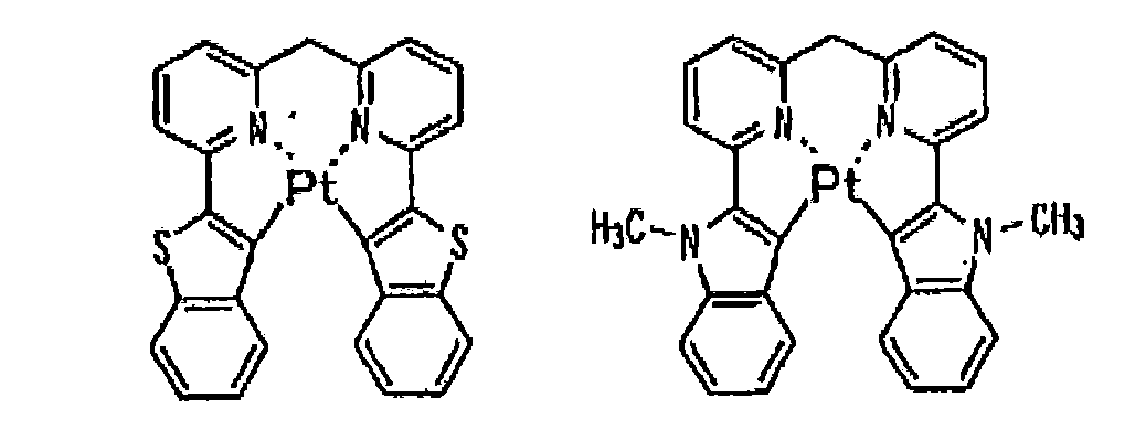


- The phosphorescent material is not particularly limited and may be appropriately selected depending on the intended purpose. Preferred are compounds represented by the following General Formulas (1), (2) and (3).


- In General Formulas (1), (2) and (3), n is an integer of 1 to 3, X-Y denotes a bidentate ligand, A denotes a ring structure which may contain a nitrogen atom, a sulfur atom or an oxygen atom, R11 represents a substituent, m1 is an integer of 0 to 6, when m1 is 2 or greater, the adjacent R11s may be bonded to form a ring which may contain a nitrogen atom, a sulfur atom or an oxygen atom and which may have a substituent, R12 represents a substituent, m2 is an integer of 0 to 4, when m2 is 2 or greater, the adjacent R12s may be bonded to form a ring which may contain a nitrogen atom, a sulfur atom or an oxygen atom and which may have a substituent, and R11 and R12 may be bonded to form a ring which may contain a nitrogen atom, a sulfur atom or an oxygen atom and which may have a substituent.
- The ring A denotes a ring structure which may contain a nitrogen atom, a sulfur atom or an oxygen atom. Preferred examples of the ring structure include 5-membered and 6-membered rings. The ring may have a substituent.
- X-Y denotes a bidentate ligand. Preferred examples thereof include bidentate monoanion ligands.
- Examples of the bidentate monoanion ligands include picolinate (pic), acetylacetonato (acac) and dipyvaloylmethanato (t-butyl acac).
- Examples of other ligands than the above ligands include ligands described on pp. 89 to 91 of International Publication No.
WO02/15645 by Lamansky, et al - The substituent represented by R11 or R12 is not particularly limited and may be appropriately selected depending on the intended purpose. Examples thereof include a halogen atom, an alkoxy group, an amino group, an alkyl group, a cycloalkyl group, an aryl group which may contain a nitrogen atom or a sulfur atom, an aryloxy group which may contain a nitrogen atom or a sulfur atom, each of the groups may further contain a substituent.
- Regarding the groups represented by R11 and R12, the adjacent groups may be bonded to form a ring which may contain a nitrogen atom, a sulfur atom or an oxygen atom. Preferred examples of the ring include 5-membered and 6-membered rings. The ring may have a substituent.
- Specific examples of the compounds represented by General Formulas (1), (2) and (3) include the following compounds but are not limited thereto.


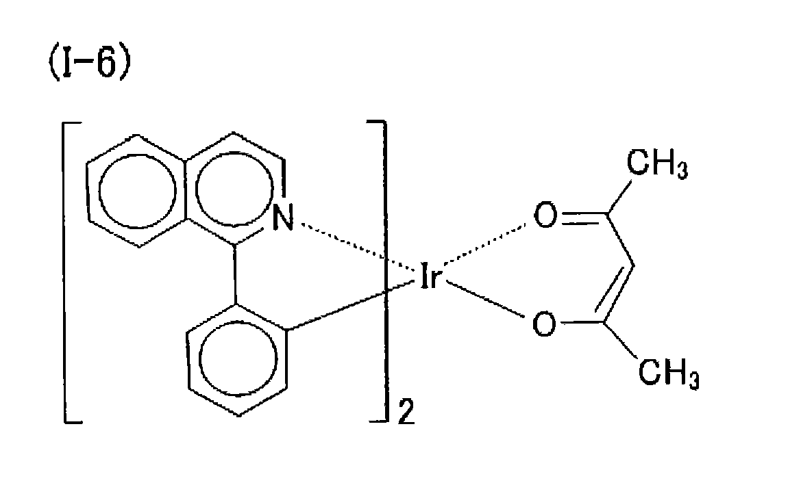


- The content of the phosphorescent material in the luminescent layer ranges preferably from 0.5% by mass to 30% by mass, more preferably 0.5% by mass to 20% by mass, still more preferably 3% by mass to 10% by mass, based on the total mass of the compounds which compose the luminescent layer.
- When the content of the phosphorescent material is less than 0.5% by mass, the luminescent efficiency may decrease. Whereas when it is more than 30% by mass, the phosphorescent materials may associate with each other to decrease the luminescent efficiency.
- The luminescent layer is a layer having a function to accept a hole from an anode, a hole injection layer and a hole transport layer, while accepting an electron from a cathode, an electron injection layer and an electron transport layer, to provide a site to recombine the hole and the electron so as to emit light.
- The thickness of the luminescent layer is not particularly limited and may be appropriately selected depending on the intended purpose. It is preferably 2 nm to 500 nm and, from the viewpoint of increasing the luminescent efficiency, is more preferably 3 nm to 200 nm, still more preferably 10 nm to 200 nm. The luminescent layer may be a single layer or two or more layers.
- The organic electroluminescent element of the present invention includes: an anode; a cathode; and an organic layer containing a luminescent layer disposed between the anode and the cathode; and, if necessary, may further include other layers depending on the intended purpose.
- The organic layer contains at least the luminescent layer; and, if necessary, may further contain, for example, an electron transport layer, an electron injection layer, a hole injection layer, a hole transport layer, a hole blocking layer and an electron blocking layer.
- The hole injection layer and the hole transport layer are layers having the function of receiving holes from the anode or from the anode side and transporting the holes to the cathode side. The hole injection layer and the hole transport layer may have a single-layered structure or a multi-layered structure made of a plurality of layers which are identical or different in composition.
- Hole injection materials or hole transport materials used for these layers may be a low-molecular-weight compound or a high-molecular-weight compound.
- Specifically, the hole injection materials or the hole transport materials are not particularly limited and may be appropriately selected depending on the intended purpose. Examples thereof include pyrrole derivatives, carbazole derivatives, triazole derivatives, oxazole derivatives, oxadiazole derivatives, imidazole derivatives, polyarylalkane derivatives, pyrazoline derivatives, pyrazolone derivatives, phenylenediamine derivatives, arylamine derivatives, amino-substituted chalcone derivatives, styrylanthracene derivatives, fluorenone derivatives, hydrazone derivatives, stilbene derivatives, silazane derivatives, aromatic tertiary amine compounds, styrylamine compounds, aromatic dimethylidine compounds, phthalocyanine compounds, porphyrin compounds, thiophene derivatives, organosilane derivatives and carbon. These may be used alone or in combination.
- Specific compounds of the hole transport materials are not particularly limited and include the above specific compounds used as the hole transport host material.
- In order to form the hole transport material into the organic deposition layer satisfying the above relationship of Ra/t, the following specific compounds are preferably used.
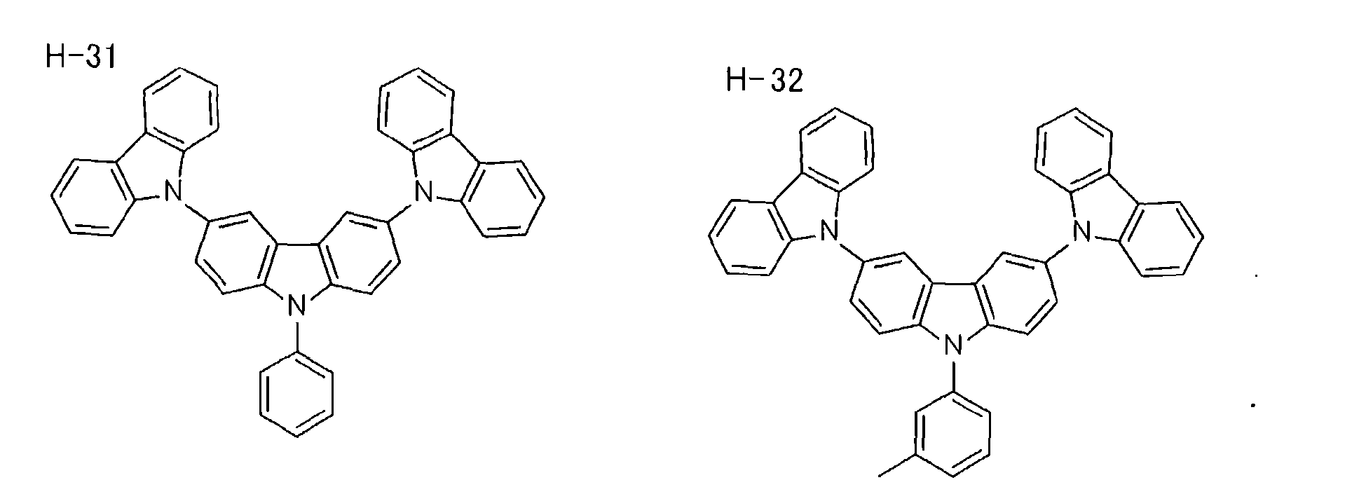


- The hole injection layer or the hole transport layer may contain an electron accepting dopant.
- The electron accepting dopant may be, for example, an inorganic or organic compound, so long as it has electron accepting property and the function of oxidizing an organic compound.
- The inorganic compound is not particularly limited and may be appropriately selected depending on the intended purpose. Examples thereof include metal halides and metal oxides.
- Examples of the metal halides include ferric chloride, aluminum chloride, gallium chloride, indium chloride and antimony pentachloride.
- Examples of the metal oxides include vanadium pentaoxide and molybdenum trioxide.
- The organic compound is not particularly limited and may be appropriately selected depending on the intended purpose. Examples thereof include compounds having a substituent such as a nitro group, a halogen, a cyano group and a trifluoromethyl group; quinone compounds; acid anhydride compounds; and fullerenes.
- These electron accepting dopants may be used alone or in combination.
- The amount of the electron accepting dopant used is not particularly limited and varies depending on the type of the material. The amount thereof is preferably 0.01% by mass to 50% by mass, more preferably 0.05% by mass to 30% by mass, particularly preferably 0.1% by mass to 30% by mass, relative to the hole transport material or the hole injection material.
- The thickness of the hole injection layer or the hole transport layer is preferably 1 nm to 500 nm, more preferably 5 nm to 250 nm, further preferably 10 nm to 200 nm.
- The electron injection layer and the electron transport layer are layers having the functions of receiving electrons from the cathode or the cathode side and transporting the electrons to the anode side. The electron-injection materials or electron-transport materials for these layers may be low-molecular-weight or high-molecular-weight compounds.
- Specific examples thereof include pyridine derivatives, quinoline derivatives, pyrimidine derivatives, pyrazine derivatives, phthalazine derivatives, phenanthoroline derivatives, triazine derivatives, triazole derivatives, oxazole derivatives, oxadiazole derivatives, imidazole derivatives, fluorenone derivatives, anthraquinodimethane derivatives, anthrone derivatives, diphenylquinone derivatives, thiopyrandioxide derivatives, carbodiimide derivatives, fluorenylidenemethane derivatives, distyrylpyradine derivatives, aryl tetracarboxylic anhydrides such as perylene and naphthalene, phthalocyanine derivatives, metal complexes (e.g., metal complexes of 8-quinolinol derivatives, metal phthalocyanine, and metal complexes containing benzoxazole or benzothiazole as the ligand) and organic silane derivatives (e.g., silole).
- The electron-injection layer or the electron-transport layer may contain an electron donating dopant. The electron donating dopant to be introduced in the electron-injection layer or the electron-transport layer is not particularly limited, so long as it has an electron-donating property and a property for reducing an organic compound, and may be appropriately selected depending on the intended purpose. Preferred examples thereof include alkali metals (e.g., Li), alkaline earth metals (e.g., Mg), transition metals including rare-earth metals, and reducing organic compounds. Among the metals, those having a work function of 4.2 eV or less are particularly preferably used. Examples thereof include Li, Na, K, Be, Mg, Ca, Sr, Ba, Y, Cs, La, Sm, Gd and Yb. Also, examples of the reducing organic compounds include nitrogen-containing compounds, sulfur-containing compounds and phosphorus-containing compounds.
- In addition, there may be used materials described in, for example,
JP-A Nos. 06-212153 2000-196140 2003-68468 2003-229278 2004-342614 - These electron donating dopants may be used alone or in combination. The amount of the electron donating dopant used depends on the type of the material, but it is preferably 0.1% by mass to 99% by mass, more preferably 1.0% by mass to 80% by mass, particularly preferably 2.0% by mass to 70% by mass, with respect to the amount of the material of the electron transport layer.
- The thicknesses of the electron-injection layer and the electron-transport layer are each preferably 500 nm or less in terms of reducing drive voltage.
- The thickness of the electron-transport layer is preferably 1 nm to 500 nm, more preferably 5 nm to 200 nm, still more preferably 10 nm to 100 nm. The thickness of the electron-injection layer is preferably 0.1 nm to 200 nm, more preferably 0.2 nm to 100 nm, still more preferably 0.5 nm to 50 nm.
- Each of the electron-injection layer and the electron-transport layer may have a single-layered structure made of one or more of the above-mentioned materials, or a multi-layered structure made of a plurality of layers which are identical or different in composition.
- The hole blocking layer is a layer having the function of preventing the holes, which have been transported from the anode side to the luminescent layer, from passing toward the cathode side, and is generally provided as an organic compound layer adjacent to the luminescent layer on the cathode side.
- The electron blocking layer is a layer having the function of preventing the electrons, which have been transported from the cathode side to the luminescent layer, from passing toward the anode side, and is generally provided as an organic compound layer adjacent to the luminescent layer on the anode side.
- The compound forming the hole blocking layer is not particularly limited and may be appropriately selected depending on the intended purpose. Examples thereof include aluminum complexes (e.g., BAlq), triazole derivatives and phenanthroline derivatives (e.g., BCP).
- Examples of the compound forming the electron blocking layer include those listed as a hole-transport material.
- The thickness of the hole blocking layer or the electron blocking layer is preferably 1 nm to 200 nm, more preferably 1 nm to 50 nm, still more preferably 3 nm to 10 nm. The hole blocking layer or the electron blocking layer may have a single-layered structure made of one or more of the aforementioned materials, or a multi-layered structure made of a plurality of layers which are identical or different in composition.
- The organic electroluminescent element of the present invention includes pair of electrodes; i.e., an anode and a cathode. In terms of the function of the organic electroluminescent element, at least one of the anode and the cathode is preferably transparent. In general, the anode may be any material, so long as it has the function of serving as an electrode which supplies holes to the organic compound layer.
- The shape, structure, size, etc. thereof are not particularly limited and may be appropriately selected from known electrode materials depending on the intended application/purpose of the organic electroluminescent element.
- Preferred examples of the material for the electrodes include metals, alloys, metal oxides, conductive compounds and mixtures thereof.
- The material for the anode is, for example, conductive metal oxides, metals, mixtures or laminates of these metals and the conductive metal oxides, inorganic conductive materials, organic conductive materials and laminates of these materials and ITO.
- Examples of the conductive metal oxides include tin oxides doped with, for example, antimony and fluorine (ATO and FTO), tin oxide, zinc oxide, indium oxide, indium tin oxide (ITO) and indium zinc oxide (IZO).
- Examples of the metals include gold, silver, chromium and nickel.
- Examples of the inorganic conductive materials include copper iodide and copper sulfide.
- Examples of the organic conductive materials include polyaniline, polythiophene and polypyrrole. Among them, conductive metal oxides are preferred. In particular, ITO is preferred from the viewpoints of productivity, high conductivity and transparency.
- The material for the cathode is, for example, alkali metals (e.g., Li, Na, K and Cs), alkaline earth metals (e.g., Mg and Ca), gold, silver, lead, aluminum, sodium-potassium alloys, lithium-aluminum alloys, magnesium-silver alloys and rare earth metals (e.g., indium and ytterbium). These may be used alone, but it is preferred that two or more of them are used in combination from the viewpoint of satisfying both stability and electron-injection property.
- Among them, as the materials for forming the cathode, alkali metals or alkaline earth metals are preferred in terms of excellent electron-injection property, and materials containing aluminum as a major component are preferred in terms of excellent storage stability.
- The term "material containing aluminum as a major component" refers to a material composed of aluminum alone; alloys containing aluminum and 0.01% by mass to 10% by mass of an alkali or alkaline earth metal; or the mixtures thereof (e.g., lithium-aluminum alloys and magnesium-aluminum alloys).
- The method for forming the electrodes is not particularly limited and may be a known method. Examples thereof include vacuum deposition methods.
- The organic electroluminescent element of the present invention is preferably formed on a substrate, may be formed so that a substrate comes into direct contact with the electrodes, or may be formed on a substrate by the mediation of an intermediate layer.
- The material for the substrate is not particularly limited and may be appropriately selected depending on the intended purpose. Examples thereof include inorganic materials, polyesters and organic materials.
- Examples of the inorganic materials include yttria-stabilized zirconia (YSZ) and glass (e.g., alkali-free glass and soda-lime glass).
- Examples of the polyesters include polyethylene terephthalate, polybutylene phthalate and polyethylene naphthalate.
- Examples of the organic materials include polystyrene, polycarbonate, polyether sulfone, polyarylate, polyimide, polycycloolefin, norbornene resins and poly(chlorotrifluoroethylene).
- The shape, structure, size, etc. of the substrate are not particularly limited and may be appropriately selected depending on, for example, the intended application/purpose of the light-emitting device. In general, the substrate is preferably a sheet. The substrate may have a single- or multi-layered structure, and may be a single member or a combination of two or more members. The substrate may be opaque, colorless transparent, or colored transparent.
- The substrate may be provided with a moisture permeation-preventing layer (gas barrier layer) on the front or back surface thereof.
- The moisture permeation-preventing layer (gas barrier layer) is preferably made from an inorganic compound such as silicon nitride and silicon oxide.
- The moisture permeation-preventing layer (gas barrier layer) may be formed through, for example, high-frequency sputtering.
- The other components are not particularly limited and may be appropriately selected depending on the intended purpose. Examples thereof include a protective layer, a sealing container, a resin seal layer and a sealing adhesive.
- The type of the protective layer, the sealing container, the resin seal layer or the sealing adhesive is not particularly limited and may be appropriately selected depending on the intended purpose. The description of
JP-A No. 2009-152572 -
Fig. 1 is a schematic view of one exemplary layer structure of the organic electroluminescent element of the present invention. Anorganic electroluminescent element 10 has a layer structure in which aglass substrate 1 and an anode 2 (e.g., an ITO electrode), ahole injection layer 3, ahole transport layer 4, aluminescent layer 5, anelectron transport layer 6, an electron injection layer 7, a cathode 8 (e.g., anAl-Li electrode) disposed on theglass substrate 1 in this order. Notably, the anode 2 (e.g., the ITO electrode) and the cathode 8 (e.g., the Al-Li electrode) are connected together via a power source. - The organic electroluminescent element can emit light when a DC voltage (which, if necessary, contains AC components) (generally 2 volts to 15 volts) or a DC is applied to between the anode and the cathode.
- The organic electroluminescent element of the present invention can be applied to an active matrix using a thin film transistor (TFT). An active layer of the thin film transistor may be made from, for example, amorphous silicon, high-temperature polysilicon, low-temperature polysilicon, microcrystalline silicon, oxide semiconductor, organic semiconductor and carbon nanotube.
- The thin film transistor used for the organic electroluminescent element of the present invention may be those described in, for example, International Publication No.
WO2005/088726 ,JP-A No. 2006-165529 U.S. Pat. Application Publication No. 2008/0237598 . - The organic electroluminescent element of the present invention is not particularly limited. In the organic electroluminescent element, the light-extraction efficiency can be further improved by various known methods. It is possible to increase the light-extraction efficiency to improve the external quantum efficiency, for example, by processing the surface shape of the substrate (for example, by forming a fine concavo-convex pattern), by controlling the refractive index of the substrate, the ITO layer and/or the organic layer, or by controlling the thickness of the substrate, the ITO layer and/or the organic layer.
- The manner in which light is extracted from the organic electroluminescent element of the present invention may be top-emission or bottom-emission.
- The organic electroluminescent element may have a resonator structure. For example, on a transparent substrate are stacked a multi-layered film mirror composed of a plurality of laminated films having different refractive indices, a transparent or semi-transparent electrode, a luminescent layer and a metal electrode. The light generated in the luminescent layer is repeatedly reflected between the multi-layered film mirror and the metal electrode (which serve as reflection plates); i.e., is resonated.
- In another embodiment, a transparent or semi-transparent electrode and a metal electrode are stacked on a transparent substrate. In this structure, the light generated in the luminescent layer is repeatedly reflected between the transparent or semi-transparent electrode and the metal electrode (which serve as reflection plates); i.e., is resonated.
- For forming the resonance structure, an optical path length determined based on the effective refractive index of two reflection plates, and on the refractive index and the thickness of each of the layers between the reflection plates is adjusted to be an optimal value for obtaining a desired resonance wavelength.
- The calculation formula applied in the case of the first embodiment is described in
JP-A No. 09-180883 JP-A No. 2004-127795 - The application of the organic electroluminescent element of the present invention is not particularly limited and may be appropriately selected depending on the intended purpose. The organic electroluminescent element can be suitably used in, for example, display devices, displays, backlights, electrophotography, illuminating light sources, recording light sources, exposing light sources, reading light sources, markers, interior accessories and optical communication.
- As a method for forming a full color-type display, there are known, for example, as described in "Monthly Display," September 2000, pp. 33 to 37, a tricolor light emission method by arranging, on a substrate, organic electroluminescent elements corresponding to three primary colors (blue color (B), green color (G) and red color (R)); a white color method by separating white light emitted from an organic electroluminescent element for white color emission into three primary colors through a color filter; and a color conversion method by converting a blue light emitted from an organic electroluminescent element for blue light emission into red color (R) and green color (G) through a fluorescent dye layer.
- A method of the present invention for producing an organic electroluminescent element including a first electrode, at least one organic deposition layer containing a luminescent layer, and a second electrode which are formed in this order, includes a step of depositing the organic deposition layer so as to satisfy the following relationship: 0.093 < Ra/t < 0.340, where Ra denotes a surface roughness of a surface of the organic deposition layer, the surface being at the side of the second electrode, and t denotes a thickness of the organic deposition layer; and, if necessary, further includes other steps.
- Any matter described above regarding the organic electroluminescent element of the present invention can be applied to: the organic electroluminescent element including a first electrode, at least one organic deposition layer containing a luminescent layer, and a second electrode which are formed in this order; the organic deposition layer satisfying the following relationship: 0.093 < Ra/t < 0.340, where Ra denotes a surface roughness of a surface of the organic deposition layer, the surface being at the side of the second electrode, and t denotes a thickness of the organic deposition layer; and the specific deposition method.
- The other steps are not particularly limited and may be appropriately selected depending on the intended purpose. For example, any known matter can be applied to the method for producing an organic electroluminescent element.
- The present invention will next be described in detail by way of Examples, which should not be construed as limiting the present invention thereto.
- A glass substrate, 0.5 mm thickness and 2.5 cm × 2.5 cm, was placed in a washing case, where it was ultrasonically washed in 2-propanol. The thus-washed glass substrate was subjected to UV-ozone treatment for 30 minutes. Onto the resulting glass substrate, each layer described below was deposited by the vacuum deposition method.
- The deposition was conducted using a vacuum deposition apparatus (product of Tokki Corporation) and, unless otherwise specified, the deposition rate was 0.2 nm/s. The deposition rate and the thickness of each layer were determined by measuring, using a film thickness monitor (CRTM-9000, product of Ulvac, Inc.), the deposition rate of the deposition material on a crystal oscillator located distant by the same distance as that between the deposition source and the substrate.
- Also, the surface roughness Ra of the deposition layer was an average of five measurements which were obtained by measuring a 2 µm × 2 µm measurement region five times on a tapping mode using an atomic force microscope (AFM, product of KEYENCE CORPORATION, VN-8000).
- Onto the glass substrate, ITO (Indium Tin Oxide) was deposited to have a thickness of 100 nm.
- On the anode, 2-TNATA (4,4',4"-Tris(N-(2-naphthyl)-N-phenyl-amino)-triphenylamine) was deposited to form a hole injection layer having a thickness of 40 nm.
- On the hole injection layer, α-NPD (bis[N-(1-naphthyl)-N-phenyl]benzidine) was deposited to form a first hole transport layer having a thickness of 7 nm.
- On the first hole transport layer, the following
hole transport material 1 was deposited at a deposition rate of 0.05 nm/sec so as to have the intended surface roughness, to form a second hole transport layer having a thickness of 3 nm. - On the second hole transport layer, the following
host material 1 and the followingphosphorescent material 1 were deposited to have a thickness of 30 nm, to form a luminescent layer in which thehost material 1 was doped with the phosphorescent material in an amount of 15% by mass. - Notably, the surface roughness Ra of the second hole transport layer facing a luminescent layer to be formed was measured using an atomic force microscope (AFM) and a measurement sample produced in the above-described manner to have a second hole transport layer as the last layer.


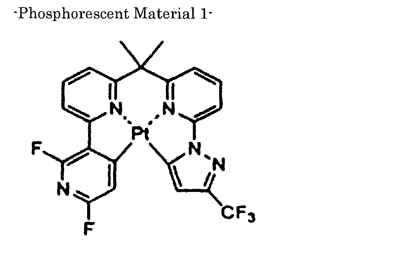
- BAlq (bis-(2-methyl-8-quinolinolato)-4-(phenyl)-phenolate-aluminium(III)) was deposited on the luminescent layer so as to have a thickness of 30 nm, to thereby form a first electron transport layer.
- LiF was deposited on the first electron transport layer so as to have a thickness of 1 nm, to thereby form a second electron transport layer.
- On the second electron transport layer, a mask patterned (giving a luminescent region of 2 mm × 2 mm) was placed before depositing metal aluminum to attain a thickness of 70 nm to form a cathode.
- The thus-produced laminate was placed in a glove box purged with argon gas and then sealed using a glass seal can and a UV curable sealant (XNR5516HV, Nagase-Ciba Ltd.) Through the above procedure, an organic electroluminescent element of Example 1 was produced.
- An organic electroluminescent element of Example 2 was produced in the same manner as in Example 1, except that the following
hole transport material 2 was used instead of thehole transport material 1 to form the second hole transport layer.
- An organic electroluminescent element of Example 3 was produced in the same manner as in Example 1, except that the following
hole transport material 3 was used instead of thehole transport material 1 to form the second hole transport layer.
- An organic electroluminescent element of Example 4 was produced in the same manner as in Example 1, except that the following
hole transport material 4 was used instead of thehole transport material 1 to form the second hole transport layer.

- An organic electroluminescent element of Comparative Example 1 was produced in the same manner as in Example 1, except that the following
hole transport material 5 was used instead of thehole transport material 1 to form the second hole transport layer.
- An organic electroluminescent element of Comparative Example 2 was produced in the same manner as in Example 1, except that the following
hole transport material 6 was used instead of thehole transport material 1 to form the second hole transport layer.

- An organic electroluminescent element of Comparative Example 3 was produced in the same manner as in Example 1, except that the following hole transport material 7 was used instead of the
hole transport material 1 to form the second hole transport layer.
- An organic electroluminescent element of Comparative Example 4 was produced in the same manner as in Example 1, except that the following
hole transport material 8 was used instead of thehole transport material 1 to form the second hole transport layer.

- An organic electroluminescent element of Comparative Example 5 was produced in the same manner as in Example 1, except that the deposition rate of the
hole transport material 1 was changed from 0.05 nm/sec to 0.005 nm/sec. - An organic electroluminescent element of Comparative Example 6 was produced in the same manner as in Example 1, except that the deposition rate of the
hole transport material 1 was changed from 0.05 nm/sec to 0.01 nm/sec. - An organic electroluminescent element of Comparative Example 7 was produced in the same manner as in Example 1, except that the deposition rate of the
hole transport material 1 was changed from 0.05 nm/sec to 0.25 nm/sec. - An organic electroluminescent element of Example 5 was produced in the same manner as in Example 1, except that the deposition rate of the
hole transport material 1 was changed from 0.05 nm/sec to 0.25 nm/sec and that the thickness of the second hole transport layer was changed from 3 nm to 10 nm. - An organic electroluminescent element of Example 6 was produced in the same manner as in Example 2, except that the deposition rate of the
hole transport material 2 was changed from 0.05 nm/sec to 0.25 nm/sec and that the thickness of the second hole transport layer was changed from 3 nm to 10 nm. - An organic electroluminescent element of Example 7 was produced in the same manner as in Comparative Example 3, except that the deposition rate of the hole transport material 7 was changed from 0.05 nm/sec to 0.25 nm/sec and that the thickness of the second hole transport layer was changed from 3 nm to 1 nm.
- An organic electroluminescent element of Comparative Example 8 was produced in the same manner as in Comparative Example 1, except that the deposition rate of the
hole transport material 5 was changed from 0.05 nm/sec to 0.025 nm/sec and that the thickness of the second hole transport layer was changed from 3 nm to 10 nm. - An organic electroluminescent element of Comparative Example 9 was produced in the same manner as in Comparative Example 3, except that the deposition rate of the hole transport material 7 was changed from 0.05 nm/sec to 0.025 nm/sec and that the thickness of the second hole transport layer was changed from 3 nm to 10 nm.
- An organic electroluminescent element of Comparative Example 10 was produced in the same manner as in Example 3, except that the deposition rate of the
hole transport material 3 was changed from 0.05 nm/sec to 0.025 nm/sec and that the thickness of the second hole transport layer was changed from 3 nm to 1 nm. - An organic electroluminescent element of Comparative Example 11 was produced in the same manner as in Example 2, except that the deposition rate of the
hole transport material 2 was changed from 0.05 nm/sec to 0.005 nm/sec. - An organic electroluminescent element of Comparative Example 12 was produced in the same manner as in Example 2, except that the deposition rate of the
hole transport material 2 was changed from 0.05 nm/sec to 0.01 nm/sec. - An organic electroluminescent element of Comparative Example 13 was produced in the same manner as in Example 2, except that the deposition rate of the
hole transport material 2 was changed from 0.05 nm/sec to 0.25 nm/sec. - An organic electroluminescent element of Comparative Example 14 was produced in the same manner as in Example 3, except that the deposition rate of the
hole transport material 3 was changed from 0.05 nm/sec to 0.005 nm/sec. - An organic electroluminescent element of Comparative Example 15 was produced in the same manner as in Example 3, except that the deposition rate of the
hole transport material 3 was changed from 0.05 nm/sec to 0.01 nm/sec. - An organic electroluminescent element of Comparative Example 16 was produced in the same manner as in Example 3, except that the deposition rate of the
hole transport material 3 was changed from 0.05 nm/sec to 0.25 nm/sec. - An organic electroluminescent element of Comparative Example 17 was produced in the same manner as in Example 4, except that the deposition rate of the
hole transport material 4 was changed from 0.05 nm/sec to 0.005 nm/sec. - An organic electroluminescent element of Comparative Example 18 was produced in the same manner as in Example 4, except that the deposition rate of the
hole transport material 4 was changed from 0.05 nm/sec to 0.01 nm/sec. - An organic electroluminescent element of Comparative Example 19 was produced in the same manner as in Example 4, except that the deposition rate of the
hole transport material 4 was changed from 0.05 nm/sec to 0.25 nm/sec. - Each of the organic electroluminescent elements of Examples 1 to 7 and Comparative Examples 1 to 19 was measured for brightness half-life from the initial brightness (2,000 cd/m2) using a durability evaluation device (product of EHC).
- The durability was evaluated based on the brightness half-life of a specific Comparative Example regarded as 100. The brightness half lives of the other Comparative Examples and Examples than the specific Comparative Example were evaluated as the relative values to that of the specific Comparative Example. For example, the organic electroluminescent element of Example 1 was found to have a brightness half-life of 313 relative to 100 of the brightness half-life of Comparative Example 1. In other words, the organic electroluminescent element of Example 1 was 3.13-fold better in durability than that of Comparative Example 1. The results are shown in the following Tables 1 to 3.
Table 1 Hole Transport Material Ra(nm) t(nm) Ra/t Brightness Half-Life Ex. 1 Hole Transport Material 10.334 3 0.111 313 Ex. 2 Hole Transport Material 20.298 3 0.099 261 Ex. 3 Hole Transport Material 30.346 3 0.115 269 Ex. 4 Hole Transport Material 40.984 3 0.328 278 Comp. Ex. 1 Hole Transport Material 50.265 3 0.088 100 Comp. Ex. 2 Hole Transport Material 60.192 3 0.064 143 Comp. Ex. 3 Hole Transport Material 7 0.232 3 0.077 188 Comp. Ex. 4 Hole Transport Material 81.129 3 0.376 149 - In Table 1, each brightness half-life is relative to the brightness half-life of Comparative Example 1 which is a standard for evaluation.
Table 2-1 Hole Transport Material Deposition rate (nm/sec) Ra(nm) t(nm) Ra/t Brightness Half-Life Ex. 1 Hole Transport Material 10.05 0.334 3 0.111 110.1 Comp. Ex. 5 Hole Transport Material 10.005 0.207 3 0.069 101.3 Comp. Ex. 6 Hole Transport Material 10.01 0.229 3 0.076 100 Comp. Ex. 7 Hole Transport Material 10.25 1.121 3 0.374 100.6 - In Table 2-1, each brightness half-life is relative to the brightness half-life of Comparative Example 6 which is a standard for evaluation.
Table 2-2 Hole Transport Material Deposition rate (nm/sec) Ra (nm) t(nm) Ra/t Brightness Half-Life Ex. 2 Hole Transport Material 20.05 0.298 3 0.099 111.7 Comp. Ex. 11 Hole Transport Material 20.005 0.198 3 0.066 97.2 Comp. Ex. 12 Hole Transport Material 20.01 0.233 3 0.078 100 Comp. Ex. 13 Hole Transport Material 20.25 1.033 3 0.344 99.8 - In Table 2-2, each brightness half-life is relative to the brightness half-life of Comparative Example 12 which is a standard for evaluation.
Table 2-3 Hole Transport Material Deposition rate (nm/sec) Ra(nm) t(nm) Ra/t Brightness Half-Life Ex. 3 Hole Transport Material 30.05 0.346 3 0.115 112.3 Comp. Ex. 14 Hole Transport Material 30.005 0.211 3 0.070 101.1 Comp. Ex. 15 Hole Transport Material 30.01 0.245 3 0.082 100 Comp. Ex. 16 Hole Transport Material 30.25 1.168 3 0.389 100.3 - In Table 2-3, each brightness half-life is relative to the brightness half-life of Comparative Example 15 which is a standard for evaluation.
Table 2-4 Hole Transport Material Deposition rate (nm/sec) Ra(nm) t(nm) Ra/t Brightness Half-Life Ex. 4 Hole Transport Material 40.05 0.984 3 0.328 110.6 Comp. Ex. 17 Hole Transport Material 40.005 0.263 3 0.088 102.4 Comp. Ex. 18 Hole Transport Material 40.01 0.276 3 0.092 100 Comp. Ex. 19 Hole Transport Material 40.25 1.356 3 0.452 96.9 - In Table 2-4, each brightness half-life is relative to the brightness half-life of Comparative Example 18 which is a standard for evaluation.
Table 3 Hole Transport Material Deposition rate (nm/sec) Ra(nm) t(nm) Ra/t Brightness Half-Life Ex. 5 Hole Transport Material 10.25 1.790 10 0.179 144 Ex. 6 Hole Transport Material 20.25 1.057 10 0.106 174 Comp. Ex. 8 Hole Transport Material 50.025 3.520 10 0.352 100 Comp. Ex. 9 Hole Transport Material 7 0.025 0.255 10 0.026 100 Ex. 7 Hole Transport Material 7 0.25 0.258 1 0.258 131 Comp. Ex. 10 Hole Transport Material 30.025 0.084 1 0.084 100 - In Table 3, the brightness half-lives of Examples 5 and 6 are relative to the brightness half-lives of Comparative Examples 8 and 9 which are a standard for evaluation, and the brightness half-life of Example 7 is relative to the brightness half-life of Comparative Example 10 which is a standard for evaluation.
- Each of the organic electroluminescent elements of Examples 1 to 7 and Comparative Examples 1 to 19 was measured for increase rate of voltage as follows.
- Specifically, the increase rate of voltage was determined based on the ratio (V100h/V0) where Vo denotes a stable drive voltage measured at the initial state of driving and V100h denotes a drive voltage after 100 hours continuous driving. Notably, the drive voltages were measured using Source Measure Unit Model 2400 (product of KEITHLEY). The drive voltage after 100 hours driving was measured after DC voltage had been applied to the organic electroluminescent element to allow it to emit light. The results are shown in the following Tables 4-1 and 4-2.
Table 4-1 Hole Transport Material Ra/t Increase Rate of Voltage After 100 h (%) Ex. 1 Hole Transport Material 10.111 6.0 Ex. 2 Hole Transport Material 20.099 5.8 Ex. 3 Hole Transport Material 30.115 4.8 Ex. 4 Hole Transport Material 40.328 5.6 Comp. Ex. 1 Hole Transport Material 50.088 10.8 Comp. Ex. 2 Hole Transport Material 60.064 7.9 Comp. Ex. 3 Hole Transport Material 7 0.077 7.9 Comp. Ex. 4 Hole Transport Material 80.376 9.3 Table 4-2 Hole Transport Material Ra/t Increase Rate of Voltage After 100 h (%) Ex. 5 Hole Transport Material 10.179 6.2 Ex. 6 Hole Transport Material 20.106 6.3 Ex. 7 Hole Transport Material 7 0.258 5.7 Comp. Ex. 5 Hole Transport Material 10.069 8.0 Comp. Ex. 6 Hole Transport Material 10.076 8.1 Comp. Ex. 7 Hole Transport Material 10.374 7.9 Comp. Ex. 8 Hole Transport Material 50.352 11.0 Comp. Ex. 9 Hole Transport Material 7 0.026 7.8 Comp. Ex. 10 Hole Transport Material 30.084 7.2 Comp. Ex. 11 Hole Transport Material 20.066 7.7 Comp. Ex. 12 Hole Transport Material 20.078 7.6 Comp. Ex. 13 Hole Transport Material 20.344 7.5 Comp. Ex. 14 Hole Transport Material 30.070 7.1 Comp. Ex. 15 Hole Transport Material 30.082 7.1 Comp. Ex. 16 Hole Transport Material 30.389 7.3 Comp. Ex. 17 Hole Transport Material 40.088 7.7 Comp. Ex. 18 Hole Transport Material 40.092 7.6 Comp. Ex. 19 Hole Transport Material 40.452 7.7 - As shown in Tables 4-1 and 4-2, the organic electroluminescent elements of Examples 1 to 7 were found to be lower in increase rate of voltage after 100 hours (%) than the organic electroluminescent elements of Comparative Examples 1 to 19.
- After each of the organic electroluminescent elements of Examples 1 to 7 and Comparative Examples 1 to 19 was driven for 100 hours, the seal can was removed and then CELLOPHANE TAPE ("CT24," product of NICHIBAN CO., 56 LTD.) was attached to the organic electroluminescent element to peel it off. The attached matter onto the tape was dissolved in a solvent, and the resultant solution was analyzed through high performance liquid chromatography. The interlayer adhesiveness was evaluated according to the following criteria:
- A: the organic materials contained in the element were not detected; and
- B: the organic materials contained in the element were detected. The results are shown in the following Tables 5-1 and 5-2.
- There was tested the extent to which the film density of each of the films formed through deposition of each hole transport material changed depending on the deposition rate at which the
hole transport materials 1 to 8 were deposited. The results are shown in the following Table 6. The film density was measured by the X-ray reflectivity method using an X-ray diffraction device ATX-G (product of Rigaku Corporation).Table 6 Film density (g/cm3) Deposition Rate (nm/sec) 0.005 0.01 0.05 0.25 Hole Transport Material 11.22 1.22 1.21 1.22 Hole Transport Material 21.22 1.22 1.23 1.23 Hole Transport Material 31.20 1.21 1.21 1.20 Hole Transport Material 41.21 1.22 1.22 1.22 Hole Transport Material 51.22 1.21 1.22 1.21 Hole Transport Material 61.21 1.21 1.20 1.22 Hole Transport Material 7 1.20 1.22 1.21 1.21 Hole Transport Material 81.23 1.22 1.23 1.22 - The present invention can provide an organic electroluminescent element having excellent durability and a method for producing the organic electroluminescent element, which are suitably be applicable in practical production of organic electroluminescent elements.
-
- 1
- Substrate
- 2
- Anode
- 3
- Hole injection layer
- 4
- Hole transport layer
- 5
- Luminescent layer
- 6
- Electron transport layer
- 7
- Electron injection layer
- 8
- Cathode
- 10
- Organic electroluminescent element
| Hole Transport Material | Ra/t | Adhesiveness | |
| Ex. 1 | | 0.111 | A |
| Ex. 2 | | 0.099 | A |
| Ex. 3 | | 0.116 | A |
| Ex. 4 | | 0.328 | A |
| Comp. Ex. 1 | | 0.088 | B |
| Comp. Ex. 2 | | 0.064 | B |
| Comp. Ex. 3 | Hole Transport Material 7 | 0.077 | B |
| Comp. Ex. 4 | | 0.376 | B |
| Hole Transport Material | Ra/t | Adhesiveness | |
| Ex. 5 | | 0.179 | A |
| Ex. 6 | | 0.106 | A |
| Ex. 7 | Hole Transport Material 7 | 0.258 | A |
| Comp. Ex. 5 | | 0.069 | B |
| Comp. Ex. 6 | | 0.076 | B |
| Comp. Ex. 7 | | 0.374 | B |
| Comp. Ex. 8 | | 0.352 | B |
| Comp. Ex. 9 | Hole Transport Material 7 | 0.026 | B |
| Comp. Ex. 10 | | 0.084 | B |
| Comp. Ex. 11 | | 0.066 | B |
| Comp. Ex. 12 | | 0.078 | B |
| Comp. Ex. 13 | | 0.344 | B |
| Comp. Ex. 14 | | 0.070 | B |
| Comp. Ex. 15 | | 0.082 | B |
| Comp. Ex. 16 | | 0.389 | B |
| Comp. Ex. 17 | | 0.088 | B |
| Comp. Ex. 18 | | 0.092 | B |
| Comp. Ex. 19 | | 0.452 | B |
Claims (8)
- An organic electroluminescent element comprising:a first electrode;at least one organic deposition layer; anda second electrode,the first electrode, the organic deposition layer, and the second electrode being formed in this order,wherein the organic deposition layer satisfies the relationship 0.093 < Ra/t < 0.340 where Ra denotes a surface roughness of a surface of the organic deposition layer, the surface being at the side of the second electrode, and t denotes a thickness of the organic deposition layer.
- The organic electroluminescent element according to claim 1, wherein the organic deposition layer contains a luminescent layer, an adjacent layer to the luminescent layer, or both of the luminescent layer and the adjacent layer.
- The organic electroluminescent element according to claim 2, wherein the adjacent layer is a hole transport layer.
- The organic electroluminescent element according to any one of claims 1 to 3, wherein the first electrode is an anode and the second electrode is a cathode.
- The organic electroluminescent element according to any one of claims 2 to 4, wherein the luminescent layer contains a phosphorescent material.
- The organic electroluminescent element according to claim 5, wherein the phosphorescent material is a platinum complex.
- The organic electroluminescent element according to any one of claims 1 to 6, wherein the thickness t of the organic deposition layer is 1 nm to 10 nm.
- A method for producing an organic electroluminescent element comprising a first electrode, at least one organic deposition layer containing a luminescent layer, and a second electrode, the first electrode, the organic deposition layer, and the second electrode being formed in this order, the method comprising:depositing the organic deposition layer so as to satisfy the relationship 0.093 < Ra/t < 0.340, where Ra denotes a surface roughness of a surface of the organic deposition layer, the surface being at the side of the second electrode, and t denotes a thickness of the organic deposition layer.
Applications Claiming Priority (2)
| Application Number | Priority Date | Filing Date | Title |
|---|---|---|---|
| JP2009180124A JP4598136B1 (en) | 2009-07-31 | 2009-07-31 | Organic electroluminescent device and manufacturing method thereof |
| PCT/JP2010/061793 WO2011013507A1 (en) | 2009-07-31 | 2010-07-12 | Organic electroluminescent element and method for manufacturing same |
Publications (2)
| Publication Number | Publication Date |
|---|---|
| EP2461386A1 true EP2461386A1 (en) | 2012-06-06 |
| EP2461386A4 EP2461386A4 (en) | 2013-01-09 |
Family
ID=43425738
Family Applications (1)
| Application Number | Title | Priority Date | Filing Date |
|---|---|---|---|
| EP10804253A Withdrawn EP2461386A4 (en) | 2009-07-31 | 2010-07-12 | Organic electroluminescent element and method for manufacturing same |
Country Status (6)
| Country | Link |
|---|---|
| US (1) | US20120126219A1 (en) |
| EP (1) | EP2461386A4 (en) |
| JP (1) | JP4598136B1 (en) |
| KR (1) | KR101190108B1 (en) |
| CN (1) | CN102484208B (en) |
| WO (1) | WO2011013507A1 (en) |
Families Citing this family (9)
| Publication number | Priority date | Publication date | Assignee | Title |
|---|---|---|---|---|
| KR101747059B1 (en) * | 2011-06-21 | 2017-07-11 | 카티바, 인크. | Materials and methods for oled microcavities and buffer layers |
| KR20150098181A (en) * | 2014-02-17 | 2015-08-27 | 삼성디스플레이 주식회사 | Organic electroluminescent device |
| KR101910112B1 (en) | 2015-05-06 | 2018-10-19 | 삼성에스디아이 주식회사 | Dopant for organic optoelectronic device and organic optoelectronic device and display device |
| US10862036B2 (en) * | 2015-06-29 | 2020-12-08 | Imec Vzw | Method for high resolution patterning of organic layers |
| US20180097202A1 (en) * | 2016-10-03 | 2018-04-05 | Regents Of The University Of Michigan | Enhanced oled outcoupling by suppressing surface plasmon modes |
| DE102017101077B4 (en) * | 2017-01-20 | 2025-06-26 | Pictiva Displays International Limited | Organic electronic component |
| TR201701604A2 (en) * | 2017-02-02 | 2018-08-27 | Elvan Gida Sanayii Ve Ticaret Anonim Sirketi | A NEW SUFLE PRODUCTION TECHNIQUE AND SUFLE PRODUCED WITH THIS TECHNIQUE |
| CN106941111A (en) * | 2017-03-14 | 2017-07-11 | 合肥鑫晟光电科技有限公司 | The manufacture method and display device of array base palte, array base palte |
| CN107104129B (en) * | 2017-05-19 | 2021-01-26 | 京东方科技集团股份有限公司 | OLED device manufacturing method, OLED device and display panel |
Family Cites Families (25)
| Publication number | Priority date | Publication date | Assignee | Title |
|---|---|---|---|---|
| JPH06212153A (en) | 1993-01-14 | 1994-08-02 | Toyo Ink Mfg Co Ltd | Organic electroluminescent device |
| JP3528470B2 (en) | 1995-10-27 | 2004-05-17 | 株式会社豊田中央研究所 | Micro-optical resonator type organic electroluminescent device |
| JP2000196140A (en) | 1998-12-28 | 2000-07-14 | Sharp Corp | Organic electroluminescent device and manufacturing method thereof |
| EP1325671B1 (en) | 2000-08-11 | 2012-10-24 | The Trustees Of Princeton University | Organometallic compounds and emission-shifting organic electrophosphorescence |
| US6579630B2 (en) | 2000-12-07 | 2003-06-17 | Canon Kabushiki Kaisha | Deuterated semiconducting organic compounds used for opto-electronic devices |
| JP2002313567A (en) | 2001-04-18 | 2002-10-25 | Sony Corp | Organic electroluminescent device and method of manufacturing the same |
| US6797314B2 (en) | 2001-07-03 | 2004-09-28 | Eastman Kodak Company | Method of handling organic material in making an organic light-emitting device |
| JP4584506B2 (en) | 2001-08-28 | 2010-11-24 | パナソニック電工株式会社 | Organic electroluminescence device |
| JP2003123967A (en) * | 2001-10-10 | 2003-04-25 | Matsushita Electric Ind Co Ltd | Light emitting device manufacturing method |
| JP3742054B2 (en) | 2001-11-30 | 2006-02-01 | 株式会社半導体エネルギー研究所 | Display device |
| JP3703028B2 (en) | 2002-10-04 | 2005-10-05 | ソニー株式会社 | Display element and display device using the same |
| US6936961B2 (en) | 2003-05-13 | 2005-08-30 | Eastman Kodak Company | Cascaded organic electroluminescent device having connecting units with N-type and P-type organic layers |
| JP2005026121A (en) * | 2003-07-03 | 2005-01-27 | Fujitsu Ltd | ORGANIC EL DEVICE, ITS MANUFACTURING METHOD, AND ORGANIC EL DISPLAY |
| KR100570978B1 (en) * | 2004-02-20 | 2006-04-13 | 삼성에스디아이 주식회사 | Organic electroluminescent display device using surface modified organic film layer and manufacturing method thereof |
| EP1737044B1 (en) | 2004-03-12 | 2014-12-10 | Japan Science and Technology Agency | Amorphous oxide and thin film transistor |
| JP4168968B2 (en) | 2004-04-26 | 2008-10-22 | セイコーエプソン株式会社 | Manufacturing method of organic EL device |
| JP5138163B2 (en) | 2004-11-10 | 2013-02-06 | キヤノン株式会社 | Field effect transistor |
| US7923128B2 (en) * | 2005-06-07 | 2011-04-12 | Fujifilm Corporation | Organic electroluminescent device |
| JP5228288B2 (en) * | 2006-06-21 | 2013-07-03 | コニカミノルタ株式会社 | Organic electroluminescence device and method for producing the same |
| JPWO2008015949A1 (en) * | 2006-08-04 | 2009-12-24 | 出光興産株式会社 | Organic electroluminescence device |
| US20080303432A1 (en) * | 2006-10-05 | 2008-12-11 | Shao Yan G | Systems and methods for improving the qualities of polymer light-emitting electrochemical cells |
| JP4613905B2 (en) | 2006-11-20 | 2011-01-19 | 日立工機株式会社 | Centrifuge rotor and centrifuge with the same |
| JP4727684B2 (en) | 2007-03-27 | 2011-07-20 | 富士フイルム株式会社 | Thin film field effect transistor and display device using the same |
| JP2009021343A (en) | 2007-07-11 | 2009-01-29 | Dainippon Printing Co Ltd | Organic electroluminescence device |
| JP5586843B2 (en) | 2007-11-27 | 2014-09-10 | ユー・ディー・シー アイルランド リミテッド | Organic electroluminescence device |
-
2009
- 2009-07-31 JP JP2009180124A patent/JP4598136B1/en active Active
-
2010
- 2010-07-12 KR KR1020127004586A patent/KR101190108B1/en active Active
- 2010-07-12 EP EP10804253A patent/EP2461386A4/en not_active Withdrawn
- 2010-07-12 CN CN201080033346.1A patent/CN102484208B/en active Active
- 2010-07-12 US US13/388,008 patent/US20120126219A1/en not_active Abandoned
- 2010-07-12 WO PCT/JP2010/061793 patent/WO2011013507A1/en not_active Ceased
Also Published As
| Publication number | Publication date |
|---|---|
| EP2461386A4 (en) | 2013-01-09 |
| JP2011034810A (en) | 2011-02-17 |
| CN102484208A (en) | 2012-05-30 |
| KR101190108B1 (en) | 2012-10-11 |
| KR20120026142A (en) | 2012-03-16 |
| WO2011013507A1 (en) | 2011-02-03 |
| CN102484208B (en) | 2013-05-15 |
| US20120126219A1 (en) | 2012-05-24 |
| JP4598136B1 (en) | 2010-12-15 |
Similar Documents
| Publication | Publication Date | Title |
|---|---|---|
| EP2461386A1 (en) | Organic electroluminescent element and method for manufacturing same | |
| US7598381B2 (en) | Near-infrared emitting organic compounds and organic devices using the same | |
| US7045952B2 (en) | OLEDs with mixed host emissive layer | |
| JP5324513B2 (en) | Organic electroluminescence device | |
| EP2549837B1 (en) | Method for producing organic electroluminescence element | |
| US20160072089A1 (en) | Light Emitting Layer-Forming Solid Material, Organic Electroluminescent Device And Method For Producing The Same | |
| JP5497510B2 (en) | Organic electroluminescence device | |
| KR20180080706A (en) | Organic electroluminescence element | |
| JP5670223B2 (en) | Organic electroluminescence device | |
| JP5649327B2 (en) | Organic electroluminescence device | |
| JP5761962B2 (en) | Organic electroluminescence device | |
| JP2011192829A (en) | Organic electroluminescent element | |
| KR101989746B1 (en) | White organic electroluminescence element | |
| JP4554721B1 (en) | Organic electroluminescence device and evaluation method thereof | |
| JP4516624B1 (en) | Inspection method for organic electroluminescence device and inspection method for material for organic electroluminescence device | |
| JPWO2014109265A1 (en) | Transparent electrode and electronic device | |
| JP5890504B2 (en) | Organic electroluminescence device | |
| JP2007103093A (en) | Organic electroluminescence device |
Legal Events
| Date | Code | Title | Description |
|---|---|---|---|
| PUAI | Public reference made under article 153(3) epc to a published international application that has entered the european phase |
Free format text: ORIGINAL CODE: 0009012 |
|
| 17P | Request for examination filed |
Effective date: 20120127 |
|
| AK | Designated contracting states |
Kind code of ref document: A1 Designated state(s): AL AT BE BG CH CY CZ DE DK EE ES FI FR GB GR HR HU IE IS IT LI LT LU LV MC MK MT NL NO PL PT RO SE SI SK SM TR |
|
| RAP1 | Party data changed (applicant data changed or rights of an application transferred) |
Owner name: UDC IRELAND LIMITED |
|
| DAX | Request for extension of the european patent (deleted) | ||
| A4 | Supplementary search report drawn up and despatched |
Effective date: 20121207 |
|
| RIC1 | Information provided on ipc code assigned before grant |
Ipc: H05B 33/10 20060101ALI20121203BHEP Ipc: H01L 51/50 20060101AFI20121203BHEP |
|
| STAA | Information on the status of an ep patent application or granted ep patent |
Free format text: STATUS: THE APPLICATION IS DEEMED TO BE WITHDRAWN |
|
| 18D | Application deemed to be withdrawn |
Effective date: 20130713 |