EP2458634A2 - Leistungsverstärkungsvorrichtung und gekoppelte Leistungsverstärkungsvorrichtung - Google Patents
Leistungsverstärkungsvorrichtung und gekoppelte Leistungsverstärkungsvorrichtung Download PDFInfo
- Publication number
- EP2458634A2 EP2458634A2 EP11175178A EP11175178A EP2458634A2 EP 2458634 A2 EP2458634 A2 EP 2458634A2 EP 11175178 A EP11175178 A EP 11175178A EP 11175178 A EP11175178 A EP 11175178A EP 2458634 A2 EP2458634 A2 EP 2458634A2
- Authority
- EP
- European Patent Office
- Prior art keywords
- source electrode
- power amplifying
- amplifying device
- earth
- electrode
- Prior art date
- Legal status (The legal status is an assumption and is not a legal conclusion. Google has not performed a legal analysis and makes no representation as to the accuracy of the status listed.)
- Granted
Links
Images


Classifications
-
- H—ELECTRICITY
- H10—SEMICONDUCTOR DEVICES; ELECTRIC SOLID-STATE DEVICES NOT OTHERWISE PROVIDED FOR
- H10W—GENERIC PACKAGES, INTERCONNECTIONS, CONNECTORS OR OTHER CONSTRUCTIONAL DETAILS OF DEVICES COVERED BY CLASS H10
- H10W20/00—Interconnections in chips, wafers or substrates
- H10W20/40—Interconnections external to wafers or substrates, e.g. back-end-of-line [BEOL] metallisations or vias connecting to gate electrodes
- H10W20/482—Interconnections external to wafers or substrates, e.g. back-end-of-line [BEOL] metallisations or vias connecting to gate electrodes for individual devices provided for in groups H10D8/00 - H10D48/00, e.g. for power transistors
- H10W20/484—Interconnections having extended contours, e.g. pads having mesh shape or interconnections comprising connected parallel stripes
-
- H—ELECTRICITY
- H10—SEMICONDUCTOR DEVICES; ELECTRIC SOLID-STATE DEVICES NOT OTHERWISE PROVIDED FOR
- H10W—GENERIC PACKAGES, INTERCONNECTIONS, CONNECTORS OR OTHER CONSTRUCTIONAL DETAILS OF DEVICES COVERED BY CLASS H10
- H10W20/00—Interconnections in chips, wafers or substrates
- H10W20/40—Interconnections external to wafers or substrates, e.g. back-end-of-line [BEOL] metallisations or vias connecting to gate electrodes
- H10W20/482—Interconnections external to wafers or substrates, e.g. back-end-of-line [BEOL] metallisations or vias connecting to gate electrodes for individual devices provided for in groups H10D8/00 - H10D48/00, e.g. for power transistors
- H10W20/483—Interconnections over air gaps, e.g. air bridges
Definitions
- the embodiment of the present invention relates to a power amplifying device and a coupled power amplifying device.
- a power amplifying element includes a drain electrode, a gate electrode, and a source electrode.
- a high frequency amplifying device includes a plurality of power electrifying elements connected in parallel to obtain a high gain.
- a coupling part for grounding source electrodes at both ends of a plurality of power amplifying elements connected in parallel and this isolated source electrode are connected by plating wiring crossing a pair of a drain electrode and a gate electrode.
- This plating wiring is referred to as air plating wiring or air bridge.
- An amplifying device is demanded which further reduces the distances from the source electrode to the via holes, and reduces an influence of an inductance as much as possible.
- the power amplifying device includes a drain electrode which is provided on a substrate, a plurality of drain fingers which is connected to the drain electrode and which has front ends branched in a comb shape, a gate electrode which faces the drain electrode and which is provided on the substrate, a plurality of gate fingers which is connected to the gate electrode and which is arranged on both sides of each drain finger, source electrodes which are arranged parallel outside the gate fingers, source electrode earth conductors which are connected to source electrodes of the source electrodes arranged outside the gate fingers arranged on both sides of the gate electrode, and which are arranged in parallel to the source electrodes, pairs of earth parts which are connected to both ends of the source electrode earth conductors and are connected with via holes for grounding, an inner source electrode of the source electrodes which is arranged between a pair of source electrode earth conductors, and an air bridge which directly connects the inner source electrode and earth parts.
- FIG. 1 is a view showing a configuration of a power amplifying device 100 according to a first application example of the present embodiment.
- the power amplifying device 100 includes pairs of earth parts 12 which are connected to the via holes 12A for grounding, source electrode earth conductors 13 which are provided on a substrate 16 and which connect these pairs of earth parts 12, source electrodes 13A which are coupled to the source electrode earth conductors 13, an inner source electrode 13B which is not in contact with the source electrode earth conductors 13, a drain electrode 14, a gate electrode 15, and an air bridge 110 which directly connects the inner source electrode 13B and the earth parts 12.
- the drain electrode 14 includes a plurality of drain fingers 14A of a comb shape.
- the gate electrode 15 includes a plurality of gate fingers of a comb shape.
- the air bridge 110 is formed with a conductor. This conductor contains gold.
- the power amplifying device 100 includes at least four earth parts 12. Hence, the power amplifying device 100 includes at least two source electrode earth conductors 13. The power amplifying device 100 includes the source electrode earth conductors 13 in parallel.
- the power amplifying device 100 includes the drain fingers 14A having front ends of a comb shape in the drain electrode 14.
- the power amplifying device 100 includes the gate fingers 15A having front ends of a comb shape in the gate electrode 15.
- the number of gate fingers 15A is double as many as the number of drain fingers 14A.
- the power amplifying device 100 includes two gate fingers 15A between the source electrode 13A and the inner source electrode 13B and includes one drain finger 14A between these two gate fingers 15A.
- the power amplifying device 100 includes four sets of source electrodes, gate electrodes, and drain electrodes.
- the inner source electrode 13B and the earth parts 12 are directly connected by the air bridge 110 including a plurality of plating wirings 11.
- the "directly connected” herein means the connection without at least source electrode earth conductors 13.
- the center of the inner source electrode 13B in a longitudinal direction is connected with the earth parts 12 at the shortest distance.
- the four earth parts 12 are diagonally connected.
- the power amplifying device 100 includes the integrally formed air bridge 120.
- the air bridge 120 has a center part 120B connected with the inner source electrode 13B, and connection bridges 120A formed on lines connecting the center of the inner source electrode 13B in the longitudinal direction with the earth parts 12 at the shortest distance.
- the air bridge 120 can be integrally formed, or can be formed by connecting the connection bridges 120A to the center part 120B later.
- the shape of the center part 120B is by no means limited.
- the center part 120B may also adopt the same shape as the inner source electrode 13B.
- connection bridge 120A is directly connected to each earth part 12.
- the air bridge 120 includes four connection bridges 120A.
- the number of connection bridges 120A can be increased or decreased within the range of limitation of design.
- the power amplifying device 100 includes the connection bridge 110 which connects the center of the inner source electrode 13B in the longitudinal direction with the earth parts 12 at the shortest distance.
- the distances from the inner source electrode 13B to the via holes 12A become the shortest, so that it is possible to minimize the influence of an inductance due to arrangement of plating wirings, which provides an effect of preventing a decrease in a gain of a high frequency amplifying device.
- FIG. 2 is a view showing a configuration of the power amplifying device 100 according to a second application example.
- the power amplifying device 100 includes the earth parts 12, the source electrode earth conductors 13, the source electrodes 13A, the inner source electrode 13B, the drain fingers 14A, and the gate fingers 15A, similarly to the first application example.
- the power amplifying device 100 includes an integrally formed air bridge 130.
- the air bridge 130 has a center part 130B connected with the inner source electrode 13B, and connection bridges 130A formed on lines connecting the ends of the inner source electrode 13B in the longitudinal direction with the closest earth parts 12 at the shortest distance.
- the air bridge 130 can be integrally formed, or can be formed by connecting the connection bridges 130A to the center part 130B later.
- the shape of the center part 130B is by no means limited.
- the center part 130B may also adopt the same shape as the inner source electrode 13B.
- connection bridge 130A is directly connected to each earth part 12.
- the air bridge 130 includes four connection bridges 130A.
- the number of connection bridges 130A can be increased or decreased within the range of limitation of design.
- the power amplifying device 100 includes the connection bridge 130 which has the center part 130B connected with the inner source electrode 13B, and the connection bridges 130A formed on lines connecting the ends of the inner source electrode 13B in the longitudinal direction with the closest earth parts 12 at the shortest distance.
- connection bridges 130A the shortest and equal, which provides an effect of further reducing the influence of an inductance.
- FIG. 3 is a view showing a configuration of the power amplifying device 100 according to a third application example of the present embodiment.
- the power amplifying device 100 includes the pairs of earth parts 12 which are connected with the via holes 12A for grounding, the source electrode earth conductors 13 which are provided on the substrate 16 and which connect these pairs of earth parts 12, the source electrodes 13A which are coupled to the source electrode earth conductors 13, inner source electrodes 13B which are not in contact with the source electrode earth conductors 13, the drain electrode 14, the gate electrode 15 and an air bridge 140 which directly connects the inner source electrodes 13B and the earth parts 12.
- the drain electrode 14 includes a plurality of drain fingers 14A of a comb shape.
- the gate electrode 15 includes a plurality of gate fingers of a comb shape.
- the inner source electrodes 13B are connected to and hide behind center parts 140C and 140D which will be described below.
- the air bridge 140 is formed with a conductor. This conductor contains gold.
- the power amplifying device 100 includes at least four earth parts 12. Hence, the power amplifying device 100 includes at least two source electrode earth conductors 13. The power amplifying device 100 includes the source electrode earth conductors 13 in parallel.
- the power amplifying device 100 includes the drain fingers 14A having front ends of a comb shape in the drain electrode 14.
- the power amplifying device 100 includes the gate fingers 15A having front ends of a comb shape in the gate electrode 15.
- the number of gate fingers 15A is double as many as the number of drain fingers 14A.
- the power amplifying device 100 includes two gate fingers 15A between the source electrode 13A and inner source electrode 13B closest to this source electrode 13A and between a pair of adjacent inner source electrodes 13B, respectively, and includes the one drain finger 14A between these two gate fingers 15A.
- the power amplifying device 100 includes eight sets of source electrodes, the gate electrodes, and drain electrodes.
- the power amplifying device 100 includes the integrally formed air bridge 140.
- the air bridge 140 has a center part 140C which is connected with the center inner source electrode 13B, the center parts 140D which are connected with left and right inner source electrodes 13B, the connection bridges 140A formed on lines connecting ends of the center inner source electrode 13B in the longitudinal direction with the closest earth parts 12 at the shortest distance, and connection bridges 140B formed on lines connecting ends of the left and right inner source electrodes 13B in the longitudinal direction with the closest earth parts 12 at the shortest distance.
- the power amplifying device 100 includes a plurality of inner source electrodes 13B, a plurality of center parts (140C and 140D) and a plurality of connection bridges (140A and 140B).
- the air bridge 140 can be integrally formed, or can be formed by connecting the connection bridges 140A to the center parts 140C and 140D later.
- the shapes of the center part 140C and the center parts 140D are by no means limited.
- the center part 140C and center parts 140D may also adopt the same shape as the inner source electrodes 13B.
- connection bridge 140A is directly connected to each earth part 12.
- the air bridge 140 includes four connection bridges 140A and four connection bridges 140B in total including two for each of the left and right inner source electrodes 13B.
- the number of the connection bridges 140A and the connection bridges 140B can be increased or decreased within the range of limitation of design.
- the power amplifying device 100 includes the connection bridge 140 which has the center parts 140C and 140D connected with the inner source electrodes 13B, and the connection bridges 140A and 140B formed on lines connecting the ends of the inner source electrodes 13B in the longitudinal direction with the closest earth parts 12 at the shortest distance.
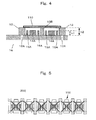
- FIG. 4 is a view showing a configuration of the power amplifying device 100 which can be commonly realized in each application example.
- FIG. 4 shows the first application example as an example.
- FIG. 4 is a sectional view showing FIG. 1 from an A-A line.
- the heights h2 of the earth parts 12 and the inner source electrode 13B are equal, and these heights h2 are higher than the heights h1 of the source electrodes 13A, the drain fingers 14A, and the gate fingers 15A.
- each air bridge (110, 120, 130, and 140) has a plane shape without an arc.
- the distances from the inner source electrode 13B to the via holes 12A further become short, so that it is possible to further reduce the influence of an inductance due to arrangement of plating wirings, which provides an effect of preventing a decrease in a gain of a high frequency amplifying device.
- FIG. 5 is a view showing an example of a plurality of coupled power amplifying devices 100 according to each application example.
- a plurality of power amplifying devices 100 according to the present embodiment can be coupled and used.
- the power amplifying devices 100 are coupled, two adjacent power amplifying devices 100 are coupled to share the source electrode earth conductor 13 which connects a pair of earth parts 12.
- a coupled power amplifying device 200 includes a plurality of power amplifying devices 100.
- the coupled power amplifying device 200 provides an effect of saving space more than that in a case where a plurality of power amplifying devices 100 is provided.
Landscapes
- Junction Field-Effect Transistors (AREA)
- Internal Circuitry In Semiconductor Integrated Circuit Devices (AREA)
- Amplifiers (AREA)
Applications Claiming Priority (1)
| Application Number | Priority Date | Filing Date | Title |
|---|---|---|---|
| JP2010263451A JP5269045B2 (ja) | 2010-11-26 | 2010-11-26 | 電力増幅装置及び連結電力増幅装置 |
Publications (3)
| Publication Number | Publication Date |
|---|---|
| EP2458634A2 true EP2458634A2 (de) | 2012-05-30 |
| EP2458634A3 EP2458634A3 (de) | 2013-02-20 |
| EP2458634B1 EP2458634B1 (de) | 2019-12-18 |
Family
ID=44582283
Family Applications (1)
| Application Number | Title | Priority Date | Filing Date |
|---|---|---|---|
| EP11175178.0A Active EP2458634B1 (de) | 2010-11-26 | 2011-07-25 | Leistungsverstärkungsvorrichtung und gekoppelte Leistungsverstärkungsvorrichtung |
Country Status (3)
| Country | Link |
|---|---|
| US (1) | US8482354B2 (de) |
| EP (1) | EP2458634B1 (de) |
| JP (1) | JP5269045B2 (de) |
Families Citing this family (2)
| Publication number | Priority date | Publication date | Assignee | Title |
|---|---|---|---|---|
| US8928411B2 (en) * | 2012-12-31 | 2015-01-06 | Silicon Image, Inc. | Integration of signal sampling within transistor amplifier stage |
| DE112017007395T5 (de) * | 2017-04-04 | 2019-12-12 | Mitsubishi Electric Corporation | Halbleitervorrichtung und Verfahren zum Herstellen derselben |
Citations (1)
| Publication number | Priority date | Publication date | Assignee | Title |
|---|---|---|---|---|
| JP2010263451A (ja) | 2009-05-08 | 2010-11-18 | Fujitsu Ltd | 受信装置、送受信装置、及び伝送システム |
Family Cites Families (8)
| Publication number | Priority date | Publication date | Assignee | Title |
|---|---|---|---|---|
| JPH0637308A (ja) | 1992-07-17 | 1994-02-10 | Murata Mfg Co Ltd | 半導体装置 |
| JPH06326330A (ja) * | 1993-05-13 | 1994-11-25 | Mitsubishi Electric Corp | 半導体装置及びその製造方法 |
| JP3144205B2 (ja) * | 1994-02-24 | 2001-03-12 | 富士通株式会社 | 超高周波装置 |
| JP3499103B2 (ja) * | 1997-02-21 | 2004-02-23 | 三菱電機株式会社 | 半導体装置 |
| JP2000138236A (ja) * | 1998-08-26 | 2000-05-16 | Mitsubishi Electric Corp | 半導体装置 |
| EP1400012B1 (de) * | 2000-10-10 | 2011-08-31 | California Institute Of Technology | Verteilte leistungsverstärkerarchitektur mit kreisförmiger geometrie |
| JP2008042184A (ja) * | 2006-07-12 | 2008-02-21 | Toshiba Corp | 高周波用半導体装置 |
| JP4743077B2 (ja) * | 2006-10-23 | 2011-08-10 | 三菱電機株式会社 | 高周波電力増幅器 |
-
2010
- 2010-11-26 JP JP2010263451A patent/JP5269045B2/ja not_active Expired - Fee Related
-
2011
- 2011-07-25 EP EP11175178.0A patent/EP2458634B1/de active Active
- 2011-07-28 US US13/192,751 patent/US8482354B2/en not_active Expired - Fee Related
Patent Citations (1)
| Publication number | Priority date | Publication date | Assignee | Title |
|---|---|---|---|---|
| JP2010263451A (ja) | 2009-05-08 | 2010-11-18 | Fujitsu Ltd | 受信装置、送受信装置、及び伝送システム |
Also Published As
| Publication number | Publication date |
|---|---|
| EP2458634A3 (de) | 2013-02-20 |
| US8482354B2 (en) | 2013-07-09 |
| US20120133440A1 (en) | 2012-05-31 |
| JP5269045B2 (ja) | 2013-08-21 |
| EP2458634B1 (de) | 2019-12-18 |
| JP2012114330A (ja) | 2012-06-14 |
Similar Documents
| Publication | Publication Date | Title |
|---|---|---|
| KR102552614B1 (ko) | 연성회로기판 | |
| US10687415B2 (en) | Flexible printed circuit board | |
| US9559401B2 (en) | Printed board and wiring arrangement method | |
| US9136623B2 (en) | Connector | |
| US20170244378A1 (en) | Surface acoustic wave device for suppressing transverse mode | |
| US9142920B2 (en) | Connector with differential pairs | |
| JPWO2010098191A1 (ja) | 導波管マイクロストリップ線路変換器 | |
| CN104009308A (zh) | 连接器 | |
| US11990699B2 (en) | Connector and connector set including a terminal abutting a side wall member | |
| CN106104923A (zh) | 微带天线 | |
| US9583881B2 (en) | Electrical connector | |
| EP3790114A1 (de) | Spaltringresonator und substrat | |
| CN104081471B (zh) | 扁平电缆 | |
| EP2458634B1 (de) | Leistungsverstärkungsvorrichtung und gekoppelte Leistungsverstärkungsvorrichtung | |
| US20170069945A1 (en) | High-frequency signal transmission line | |
| US10057977B2 (en) | Wiring board and electronic device | |
| US20100177004A1 (en) | Multi-band printed antenna | |
| KR101159456B1 (ko) | 신호 효율이 최대화된 전송선 변압기 | |
| US20200352024A1 (en) | Structure and wiring substrate | |
| US9591759B2 (en) | Circuit board | |
| JP2009302099A (ja) | 半導体装置 | |
| US9601874B2 (en) | Connector and transmission line structure | |
| TWI658646B (zh) | 天線裝置 | |
| US12603409B2 (en) | High-frequency transmission element | |
| EP2566050A1 (de) | Verbundkomponente |
Legal Events
| Date | Code | Title | Description |
|---|---|---|---|
| PUAI | Public reference made under article 153(3) epc to a published international application that has entered the european phase |
Free format text: ORIGINAL CODE: 0009012 |
|
| 17P | Request for examination filed |
Effective date: 20110725 |
|
| AK | Designated contracting states |
Kind code of ref document: A2 Designated state(s): AL AT BE BG CH CY CZ DE DK EE ES FI FR GB GR HR HU IE IS IT LI LT LU LV MC MK MT NL NO PL PT RO RS SE SI SK SM TR |
|
| AX | Request for extension of the european patent |
Extension state: BA ME |
|
| PUAL | Search report despatched |
Free format text: ORIGINAL CODE: 0009013 |
|
| AK | Designated contracting states |
Kind code of ref document: A3 Designated state(s): AL AT BE BG CH CY CZ DE DK EE ES FI FR GB GR HR HU IE IS IT LI LT LU LV MC MK MT NL NO PL PT RO RS SE SI SK SM TR |
|
| AX | Request for extension of the european patent |
Extension state: BA ME |
|
| RIC1 | Information provided on ipc code assigned before grant |
Ipc: H01L 23/482 20060101AFI20130111BHEP |
|
| STAA | Information on the status of an ep patent application or granted ep patent |
Free format text: STATUS: EXAMINATION IS IN PROGRESS |
|
| 17Q | First examination report despatched |
Effective date: 20161128 |
|
| GRAP | Despatch of communication of intention to grant a patent |
Free format text: ORIGINAL CODE: EPIDOSNIGR1 |
|
| STAA | Information on the status of an ep patent application or granted ep patent |
Free format text: STATUS: GRANT OF PATENT IS INTENDED |
|
| INTG | Intention to grant announced |
Effective date: 20170530 |
|
| GRAJ | Information related to disapproval of communication of intention to grant by the applicant or resumption of examination proceedings by the epo deleted |
Free format text: ORIGINAL CODE: EPIDOSDIGR1 |
|
| STAA | Information on the status of an ep patent application or granted ep patent |
Free format text: STATUS: EXAMINATION IS IN PROGRESS |
|
| INTC | Intention to grant announced (deleted) | ||
| GRAS | Grant fee paid |
Free format text: ORIGINAL CODE: EPIDOSNIGR3 |
|
| STAA | Information on the status of an ep patent application or granted ep patent |
Free format text: STATUS: GRANT OF PATENT IS INTENDED |
|
| GRAP | Despatch of communication of intention to grant a patent |
Free format text: ORIGINAL CODE: EPIDOSNIGR1 |
|
| INTG | Intention to grant announced |
Effective date: 20190802 |
|
| GRAA | (expected) grant |
Free format text: ORIGINAL CODE: 0009210 |
|
| STAA | Information on the status of an ep patent application or granted ep patent |
Free format text: STATUS: THE PATENT HAS BEEN GRANTED |
|
| AK | Designated contracting states |
Kind code of ref document: B1 Designated state(s): AL AT BE BG CH CY CZ DE DK EE ES FI FR GB GR HR HU IE IS IT LI LT LU LV MC MK MT NL NO PL PT RO RS SE SI SK SM TR |
|
| REG | Reference to a national code |
Ref country code: GB Ref legal event code: FG4D |
|
| REG | Reference to a national code |
Ref country code: CH Ref legal event code: EP |
|
| REG | Reference to a national code |
Ref country code: DE Ref legal event code: R096 Ref document number: 602011064059 Country of ref document: DE |
|
| REG | Reference to a national code |
Ref country code: IE Ref legal event code: FG4D |
|
| REG | Reference to a national code |
Ref country code: AT Ref legal event code: REF Ref document number: 1215535 Country of ref document: AT Kind code of ref document: T Effective date: 20200115 |
|
| REG | Reference to a national code |
Ref country code: NL Ref legal event code: MP Effective date: 20191218 |
|
| PG25 | Lapsed in a contracting state [announced via postgrant information from national office to epo] |
Ref country code: NO Free format text: LAPSE BECAUSE OF FAILURE TO SUBMIT A TRANSLATION OF THE DESCRIPTION OR TO PAY THE FEE WITHIN THE PRESCRIBED TIME-LIMIT Effective date: 20200318 Ref country code: BG Free format text: LAPSE BECAUSE OF FAILURE TO SUBMIT A TRANSLATION OF THE DESCRIPTION OR TO PAY THE FEE WITHIN THE PRESCRIBED TIME-LIMIT Effective date: 20200318 Ref country code: LT Free format text: LAPSE BECAUSE OF FAILURE TO SUBMIT A TRANSLATION OF THE DESCRIPTION OR TO PAY THE FEE WITHIN THE PRESCRIBED TIME-LIMIT Effective date: 20191218 Ref country code: GR Free format text: LAPSE BECAUSE OF FAILURE TO SUBMIT A TRANSLATION OF THE DESCRIPTION OR TO PAY THE FEE WITHIN THE PRESCRIBED TIME-LIMIT Effective date: 20200319 Ref country code: SE Free format text: LAPSE BECAUSE OF FAILURE TO SUBMIT A TRANSLATION OF THE DESCRIPTION OR TO PAY THE FEE WITHIN THE PRESCRIBED TIME-LIMIT Effective date: 20191218 Ref country code: LV Free format text: LAPSE BECAUSE OF FAILURE TO SUBMIT A TRANSLATION OF THE DESCRIPTION OR TO PAY THE FEE WITHIN THE PRESCRIBED TIME-LIMIT Effective date: 20191218 Ref country code: FI Free format text: LAPSE BECAUSE OF FAILURE TO SUBMIT A TRANSLATION OF THE DESCRIPTION OR TO PAY THE FEE WITHIN THE PRESCRIBED TIME-LIMIT Effective date: 20191218 |
|
| REG | Reference to a national code |
Ref country code: LT Ref legal event code: MG4D |
|
| PG25 | Lapsed in a contracting state [announced via postgrant information from national office to epo] |
Ref country code: RS Free format text: LAPSE BECAUSE OF FAILURE TO SUBMIT A TRANSLATION OF THE DESCRIPTION OR TO PAY THE FEE WITHIN THE PRESCRIBED TIME-LIMIT Effective date: 20191218 Ref country code: HR Free format text: LAPSE BECAUSE OF FAILURE TO SUBMIT A TRANSLATION OF THE DESCRIPTION OR TO PAY THE FEE WITHIN THE PRESCRIBED TIME-LIMIT Effective date: 20191218 |
|
| PG25 | Lapsed in a contracting state [announced via postgrant information from national office to epo] |
Ref country code: AL Free format text: LAPSE BECAUSE OF FAILURE TO SUBMIT A TRANSLATION OF THE DESCRIPTION OR TO PAY THE FEE WITHIN THE PRESCRIBED TIME-LIMIT Effective date: 20191218 |
|
| PG25 | Lapsed in a contracting state [announced via postgrant information from national office to epo] |
Ref country code: PT Free format text: LAPSE BECAUSE OF FAILURE TO SUBMIT A TRANSLATION OF THE DESCRIPTION OR TO PAY THE FEE WITHIN THE PRESCRIBED TIME-LIMIT Effective date: 20200513 Ref country code: CZ Free format text: LAPSE BECAUSE OF FAILURE TO SUBMIT A TRANSLATION OF THE DESCRIPTION OR TO PAY THE FEE WITHIN THE PRESCRIBED TIME-LIMIT Effective date: 20191218 Ref country code: NL Free format text: LAPSE BECAUSE OF FAILURE TO SUBMIT A TRANSLATION OF THE DESCRIPTION OR TO PAY THE FEE WITHIN THE PRESCRIBED TIME-LIMIT Effective date: 20191218 Ref country code: RO Free format text: LAPSE BECAUSE OF FAILURE TO SUBMIT A TRANSLATION OF THE DESCRIPTION OR TO PAY THE FEE WITHIN THE PRESCRIBED TIME-LIMIT Effective date: 20191218 Ref country code: EE Free format text: LAPSE BECAUSE OF FAILURE TO SUBMIT A TRANSLATION OF THE DESCRIPTION OR TO PAY THE FEE WITHIN THE PRESCRIBED TIME-LIMIT Effective date: 20191218 |
|
| PG25 | Lapsed in a contracting state [announced via postgrant information from national office to epo] |
Ref country code: IS Free format text: LAPSE BECAUSE OF FAILURE TO SUBMIT A TRANSLATION OF THE DESCRIPTION OR TO PAY THE FEE WITHIN THE PRESCRIBED TIME-LIMIT Effective date: 20200418 Ref country code: SK Free format text: LAPSE BECAUSE OF FAILURE TO SUBMIT A TRANSLATION OF THE DESCRIPTION OR TO PAY THE FEE WITHIN THE PRESCRIBED TIME-LIMIT Effective date: 20191218 Ref country code: SM Free format text: LAPSE BECAUSE OF FAILURE TO SUBMIT A TRANSLATION OF THE DESCRIPTION OR TO PAY THE FEE WITHIN THE PRESCRIBED TIME-LIMIT Effective date: 20191218 |
|
| REG | Reference to a national code |
Ref country code: DE Ref legal event code: R097 Ref document number: 602011064059 Country of ref document: DE |
|
| REG | Reference to a national code |
Ref country code: AT Ref legal event code: MK05 Ref document number: 1215535 Country of ref document: AT Kind code of ref document: T Effective date: 20191218 |
|
| PLBE | No opposition filed within time limit |
Free format text: ORIGINAL CODE: 0009261 |
|
| STAA | Information on the status of an ep patent application or granted ep patent |
Free format text: STATUS: NO OPPOSITION FILED WITHIN TIME LIMIT |
|
| PG25 | Lapsed in a contracting state [announced via postgrant information from national office to epo] |
Ref country code: ES Free format text: LAPSE BECAUSE OF FAILURE TO SUBMIT A TRANSLATION OF THE DESCRIPTION OR TO PAY THE FEE WITHIN THE PRESCRIBED TIME-LIMIT Effective date: 20191218 Ref country code: DK Free format text: LAPSE BECAUSE OF FAILURE TO SUBMIT A TRANSLATION OF THE DESCRIPTION OR TO PAY THE FEE WITHIN THE PRESCRIBED TIME-LIMIT Effective date: 20191218 |
|
| 26N | No opposition filed |
Effective date: 20200921 |
|
| PG25 | Lapsed in a contracting state [announced via postgrant information from national office to epo] |
Ref country code: AT Free format text: LAPSE BECAUSE OF FAILURE TO SUBMIT A TRANSLATION OF THE DESCRIPTION OR TO PAY THE FEE WITHIN THE PRESCRIBED TIME-LIMIT Effective date: 20191218 Ref country code: SI Free format text: LAPSE BECAUSE OF FAILURE TO SUBMIT A TRANSLATION OF THE DESCRIPTION OR TO PAY THE FEE WITHIN THE PRESCRIBED TIME-LIMIT Effective date: 20191218 |
|
| PG25 | Lapsed in a contracting state [announced via postgrant information from national office to epo] |
Ref country code: IT Free format text: LAPSE BECAUSE OF FAILURE TO SUBMIT A TRANSLATION OF THE DESCRIPTION OR TO PAY THE FEE WITHIN THE PRESCRIBED TIME-LIMIT Effective date: 20191218 |
|
| PG25 | Lapsed in a contracting state [announced via postgrant information from national office to epo] |
Ref country code: PL Free format text: LAPSE BECAUSE OF FAILURE TO SUBMIT A TRANSLATION OF THE DESCRIPTION OR TO PAY THE FEE WITHIN THE PRESCRIBED TIME-LIMIT Effective date: 20191218 Ref country code: MC Free format text: LAPSE BECAUSE OF FAILURE TO SUBMIT A TRANSLATION OF THE DESCRIPTION OR TO PAY THE FEE WITHIN THE PRESCRIBED TIME-LIMIT Effective date: 20191218 |
|
| REG | Reference to a national code |
Ref country code: CH Ref legal event code: PL |
|
| REG | Reference to a national code |
Ref country code: BE Ref legal event code: MM Effective date: 20200731 |
|
| PG25 | Lapsed in a contracting state [announced via postgrant information from national office to epo] |
Ref country code: LU Free format text: LAPSE BECAUSE OF NON-PAYMENT OF DUE FEES Effective date: 20200725 Ref country code: CH Free format text: LAPSE BECAUSE OF NON-PAYMENT OF DUE FEES Effective date: 20200731 Ref country code: LI Free format text: LAPSE BECAUSE OF NON-PAYMENT OF DUE FEES Effective date: 20200731 |
|
| PG25 | Lapsed in a contracting state [announced via postgrant information from national office to epo] |
Ref country code: BE Free format text: LAPSE BECAUSE OF NON-PAYMENT OF DUE FEES Effective date: 20200731 |
|
| PG25 | Lapsed in a contracting state [announced via postgrant information from national office to epo] |
Ref country code: IE Free format text: LAPSE BECAUSE OF NON-PAYMENT OF DUE FEES Effective date: 20200725 |
|
| PG25 | Lapsed in a contracting state [announced via postgrant information from national office to epo] |
Ref country code: TR Free format text: LAPSE BECAUSE OF FAILURE TO SUBMIT A TRANSLATION OF THE DESCRIPTION OR TO PAY THE FEE WITHIN THE PRESCRIBED TIME-LIMIT Effective date: 20191218 Ref country code: MT Free format text: LAPSE BECAUSE OF FAILURE TO SUBMIT A TRANSLATION OF THE DESCRIPTION OR TO PAY THE FEE WITHIN THE PRESCRIBED TIME-LIMIT Effective date: 20191218 Ref country code: CY Free format text: LAPSE BECAUSE OF FAILURE TO SUBMIT A TRANSLATION OF THE DESCRIPTION OR TO PAY THE FEE WITHIN THE PRESCRIBED TIME-LIMIT Effective date: 20191218 |
|
| PG25 | Lapsed in a contracting state [announced via postgrant information from national office to epo] |
Ref country code: MK Free format text: LAPSE BECAUSE OF FAILURE TO SUBMIT A TRANSLATION OF THE DESCRIPTION OR TO PAY THE FEE WITHIN THE PRESCRIBED TIME-LIMIT Effective date: 20191218 |
|
| PGFP | Annual fee paid to national office [announced via postgrant information from national office to epo] |
Ref country code: GB Payment date: 20250605 Year of fee payment: 15 |
|
| PGFP | Annual fee paid to national office [announced via postgrant information from national office to epo] |
Ref country code: FR Payment date: 20250610 Year of fee payment: 15 |
|
| PGFP | Annual fee paid to national office [announced via postgrant information from national office to epo] |
Ref country code: DE Payment date: 20250528 Year of fee payment: 15 |
|
| REG | Reference to a national code |
Ref country code: DE Ref legal event code: R079 Ref document number: 602011064059 Country of ref document: DE Free format text: PREVIOUS MAIN CLASS: H01L0023482000 Ipc: H10W0072000000 |