EP2458634A2 - Power amplifying device and coupled power amplifying device - Google Patents
Power amplifying device and coupled power amplifying device Download PDFInfo
- Publication number
- EP2458634A2 EP2458634A2 EP11175178A EP11175178A EP2458634A2 EP 2458634 A2 EP2458634 A2 EP 2458634A2 EP 11175178 A EP11175178 A EP 11175178A EP 11175178 A EP11175178 A EP 11175178A EP 2458634 A2 EP2458634 A2 EP 2458634A2
- Authority
- EP
- European Patent Office
- Prior art keywords
- source electrode
- power amplifying
- amplifying device
- earth
- electrode
- Prior art date
- Legal status (The legal status is an assumption and is not a legal conclusion. Google has not performed a legal analysis and makes no representation as to the accuracy of the status listed.)
- Granted
Links
Images


Classifications
-
- H—ELECTRICITY
- H10—SEMICONDUCTOR DEVICES; ELECTRIC SOLID-STATE DEVICES NOT OTHERWISE PROVIDED FOR
- H10W—GENERIC PACKAGES, INTERCONNECTIONS, CONNECTORS OR OTHER CONSTRUCTIONAL DETAILS OF DEVICES COVERED BY CLASS H10
- H10W20/00—Interconnections in chips, wafers or substrates
- H10W20/40—Interconnections external to wafers or substrates, e.g. back-end-of-line [BEOL] metallisations or vias connecting to gate electrodes
- H10W20/482—Interconnections external to wafers or substrates, e.g. back-end-of-line [BEOL] metallisations or vias connecting to gate electrodes for individual devices provided for in groups H10D8/00 - H10D48/00, e.g. for power transistors
- H10W20/484—Interconnections having extended contours, e.g. pads having mesh shape or interconnections comprising connected parallel stripes
-
- H—ELECTRICITY
- H10—SEMICONDUCTOR DEVICES; ELECTRIC SOLID-STATE DEVICES NOT OTHERWISE PROVIDED FOR
- H10W—GENERIC PACKAGES, INTERCONNECTIONS, CONNECTORS OR OTHER CONSTRUCTIONAL DETAILS OF DEVICES COVERED BY CLASS H10
- H10W20/00—Interconnections in chips, wafers or substrates
- H10W20/40—Interconnections external to wafers or substrates, e.g. back-end-of-line [BEOL] metallisations or vias connecting to gate electrodes
- H10W20/482—Interconnections external to wafers or substrates, e.g. back-end-of-line [BEOL] metallisations or vias connecting to gate electrodes for individual devices provided for in groups H10D8/00 - H10D48/00, e.g. for power transistors
- H10W20/483—Interconnections over air gaps, e.g. air bridges
Definitions
- the embodiment of the present invention relates to a power amplifying device and a coupled power amplifying device.
- a power amplifying element includes a drain electrode, a gate electrode, and a source electrode.
- a high frequency amplifying device includes a plurality of power electrifying elements connected in parallel to obtain a high gain.
- a coupling part for grounding source electrodes at both ends of a plurality of power amplifying elements connected in parallel and this isolated source electrode are connected by plating wiring crossing a pair of a drain electrode and a gate electrode.
- This plating wiring is referred to as air plating wiring or air bridge.
- An amplifying device is demanded which further reduces the distances from the source electrode to the via holes, and reduces an influence of an inductance as much as possible.
- the power amplifying device includes a drain electrode which is provided on a substrate, a plurality of drain fingers which is connected to the drain electrode and which has front ends branched in a comb shape, a gate electrode which faces the drain electrode and which is provided on the substrate, a plurality of gate fingers which is connected to the gate electrode and which is arranged on both sides of each drain finger, source electrodes which are arranged parallel outside the gate fingers, source electrode earth conductors which are connected to source electrodes of the source electrodes arranged outside the gate fingers arranged on both sides of the gate electrode, and which are arranged in parallel to the source electrodes, pairs of earth parts which are connected to both ends of the source electrode earth conductors and are connected with via holes for grounding, an inner source electrode of the source electrodes which is arranged between a pair of source electrode earth conductors, and an air bridge which directly connects the inner source electrode and earth parts.
- FIG. 1 is a view showing a configuration of a power amplifying device 100 according to a first application example of the present embodiment.
- the power amplifying device 100 includes pairs of earth parts 12 which are connected to the via holes 12A for grounding, source electrode earth conductors 13 which are provided on a substrate 16 and which connect these pairs of earth parts 12, source electrodes 13A which are coupled to the source electrode earth conductors 13, an inner source electrode 13B which is not in contact with the source electrode earth conductors 13, a drain electrode 14, a gate electrode 15, and an air bridge 110 which directly connects the inner source electrode 13B and the earth parts 12.
- the drain electrode 14 includes a plurality of drain fingers 14A of a comb shape.
- the gate electrode 15 includes a plurality of gate fingers of a comb shape.
- the air bridge 110 is formed with a conductor. This conductor contains gold.
- the power amplifying device 100 includes at least four earth parts 12. Hence, the power amplifying device 100 includes at least two source electrode earth conductors 13. The power amplifying device 100 includes the source electrode earth conductors 13 in parallel.
- the power amplifying device 100 includes the drain fingers 14A having front ends of a comb shape in the drain electrode 14.
- the power amplifying device 100 includes the gate fingers 15A having front ends of a comb shape in the gate electrode 15.
- the number of gate fingers 15A is double as many as the number of drain fingers 14A.
- the power amplifying device 100 includes two gate fingers 15A between the source electrode 13A and the inner source electrode 13B and includes one drain finger 14A between these two gate fingers 15A.
- the power amplifying device 100 includes four sets of source electrodes, gate electrodes, and drain electrodes.
- the inner source electrode 13B and the earth parts 12 are directly connected by the air bridge 110 including a plurality of plating wirings 11.
- the "directly connected” herein means the connection without at least source electrode earth conductors 13.
- the center of the inner source electrode 13B in a longitudinal direction is connected with the earth parts 12 at the shortest distance.
- the four earth parts 12 are diagonally connected.
- the power amplifying device 100 includes the integrally formed air bridge 120.
- the air bridge 120 has a center part 120B connected with the inner source electrode 13B, and connection bridges 120A formed on lines connecting the center of the inner source electrode 13B in the longitudinal direction with the earth parts 12 at the shortest distance.
- the air bridge 120 can be integrally formed, or can be formed by connecting the connection bridges 120A to the center part 120B later.
- the shape of the center part 120B is by no means limited.
- the center part 120B may also adopt the same shape as the inner source electrode 13B.
- connection bridge 120A is directly connected to each earth part 12.
- the air bridge 120 includes four connection bridges 120A.
- the number of connection bridges 120A can be increased or decreased within the range of limitation of design.
- the power amplifying device 100 includes the connection bridge 110 which connects the center of the inner source electrode 13B in the longitudinal direction with the earth parts 12 at the shortest distance.
- the distances from the inner source electrode 13B to the via holes 12A become the shortest, so that it is possible to minimize the influence of an inductance due to arrangement of plating wirings, which provides an effect of preventing a decrease in a gain of a high frequency amplifying device.
- FIG. 2 is a view showing a configuration of the power amplifying device 100 according to a second application example.
- the power amplifying device 100 includes the earth parts 12, the source electrode earth conductors 13, the source electrodes 13A, the inner source electrode 13B, the drain fingers 14A, and the gate fingers 15A, similarly to the first application example.
- the power amplifying device 100 includes an integrally formed air bridge 130.
- the air bridge 130 has a center part 130B connected with the inner source electrode 13B, and connection bridges 130A formed on lines connecting the ends of the inner source electrode 13B in the longitudinal direction with the closest earth parts 12 at the shortest distance.
- the air bridge 130 can be integrally formed, or can be formed by connecting the connection bridges 130A to the center part 130B later.
- the shape of the center part 130B is by no means limited.
- the center part 130B may also adopt the same shape as the inner source electrode 13B.
- connection bridge 130A is directly connected to each earth part 12.
- the air bridge 130 includes four connection bridges 130A.
- the number of connection bridges 130A can be increased or decreased within the range of limitation of design.
- the power amplifying device 100 includes the connection bridge 130 which has the center part 130B connected with the inner source electrode 13B, and the connection bridges 130A formed on lines connecting the ends of the inner source electrode 13B in the longitudinal direction with the closest earth parts 12 at the shortest distance.
- connection bridges 130A the shortest and equal, which provides an effect of further reducing the influence of an inductance.
- FIG. 3 is a view showing a configuration of the power amplifying device 100 according to a third application example of the present embodiment.
- the power amplifying device 100 includes the pairs of earth parts 12 which are connected with the via holes 12A for grounding, the source electrode earth conductors 13 which are provided on the substrate 16 and which connect these pairs of earth parts 12, the source electrodes 13A which are coupled to the source electrode earth conductors 13, inner source electrodes 13B which are not in contact with the source electrode earth conductors 13, the drain electrode 14, the gate electrode 15 and an air bridge 140 which directly connects the inner source electrodes 13B and the earth parts 12.
- the drain electrode 14 includes a plurality of drain fingers 14A of a comb shape.
- the gate electrode 15 includes a plurality of gate fingers of a comb shape.
- the inner source electrodes 13B are connected to and hide behind center parts 140C and 140D which will be described below.
- the air bridge 140 is formed with a conductor. This conductor contains gold.
- the power amplifying device 100 includes at least four earth parts 12. Hence, the power amplifying device 100 includes at least two source electrode earth conductors 13. The power amplifying device 100 includes the source electrode earth conductors 13 in parallel.
- the power amplifying device 100 includes the drain fingers 14A having front ends of a comb shape in the drain electrode 14.
- the power amplifying device 100 includes the gate fingers 15A having front ends of a comb shape in the gate electrode 15.
- the number of gate fingers 15A is double as many as the number of drain fingers 14A.
- the power amplifying device 100 includes two gate fingers 15A between the source electrode 13A and inner source electrode 13B closest to this source electrode 13A and between a pair of adjacent inner source electrodes 13B, respectively, and includes the one drain finger 14A between these two gate fingers 15A.
- the power amplifying device 100 includes eight sets of source electrodes, the gate electrodes, and drain electrodes.
- the power amplifying device 100 includes the integrally formed air bridge 140.
- the air bridge 140 has a center part 140C which is connected with the center inner source electrode 13B, the center parts 140D which are connected with left and right inner source electrodes 13B, the connection bridges 140A formed on lines connecting ends of the center inner source electrode 13B in the longitudinal direction with the closest earth parts 12 at the shortest distance, and connection bridges 140B formed on lines connecting ends of the left and right inner source electrodes 13B in the longitudinal direction with the closest earth parts 12 at the shortest distance.
- the power amplifying device 100 includes a plurality of inner source electrodes 13B, a plurality of center parts (140C and 140D) and a plurality of connection bridges (140A and 140B).
- the air bridge 140 can be integrally formed, or can be formed by connecting the connection bridges 140A to the center parts 140C and 140D later.
- the shapes of the center part 140C and the center parts 140D are by no means limited.
- the center part 140C and center parts 140D may also adopt the same shape as the inner source electrodes 13B.
- connection bridge 140A is directly connected to each earth part 12.
- the air bridge 140 includes four connection bridges 140A and four connection bridges 140B in total including two for each of the left and right inner source electrodes 13B.
- the number of the connection bridges 140A and the connection bridges 140B can be increased or decreased within the range of limitation of design.
- the power amplifying device 100 includes the connection bridge 140 which has the center parts 140C and 140D connected with the inner source electrodes 13B, and the connection bridges 140A and 140B formed on lines connecting the ends of the inner source electrodes 13B in the longitudinal direction with the closest earth parts 12 at the shortest distance.
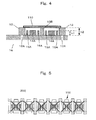
- FIG. 4 is a view showing a configuration of the power amplifying device 100 which can be commonly realized in each application example.
- FIG. 4 shows the first application example as an example.
- FIG. 4 is a sectional view showing FIG. 1 from an A-A line.
- the heights h2 of the earth parts 12 and the inner source electrode 13B are equal, and these heights h2 are higher than the heights h1 of the source electrodes 13A, the drain fingers 14A, and the gate fingers 15A.
- each air bridge (110, 120, 130, and 140) has a plane shape without an arc.
- the distances from the inner source electrode 13B to the via holes 12A further become short, so that it is possible to further reduce the influence of an inductance due to arrangement of plating wirings, which provides an effect of preventing a decrease in a gain of a high frequency amplifying device.
- FIG. 5 is a view showing an example of a plurality of coupled power amplifying devices 100 according to each application example.
- a plurality of power amplifying devices 100 according to the present embodiment can be coupled and used.
- the power amplifying devices 100 are coupled, two adjacent power amplifying devices 100 are coupled to share the source electrode earth conductor 13 which connects a pair of earth parts 12.
- a coupled power amplifying device 200 includes a plurality of power amplifying devices 100.
- the coupled power amplifying device 200 provides an effect of saving space more than that in a case where a plurality of power amplifying devices 100 is provided.
Landscapes
- Junction Field-Effect Transistors (AREA)
- Internal Circuitry In Semiconductor Integrated Circuit Devices (AREA)
- Amplifiers (AREA)
Abstract
Description
- This application is based upon and claims the benefit of priority from the prior Japanese Patent Application No.
2010-263451, filed on 26th November, 2010 - The embodiment of the present invention relates to a power amplifying device and a coupled power amplifying device.
- A power amplifying element includes a drain electrode, a gate electrode, and a source electrode. A high frequency amplifying device includes a plurality of power electrifying elements connected in parallel to obtain a high gain.
- When a plurality of drain electrodes of this high frequency amplifying device is cónnected in one direction and a plurality of gate electrodes is connected in the other direction, an isolated source electrode is left when the number of power amplifying elements is four or more, and there is an issue of how to ground this isolated source electrode.
- With a conventional high frequency amplifying device, in order to ground this isolated source electrode, a coupling part for grounding source electrodes at both ends of a plurality of power amplifying elements connected in parallel and this isolated source electrode are connected by plating wiring crossing a pair of a drain electrode and a gate electrode. This plating wiring is referred to as air plating wiring or air bridge.
- However, if the air bridge is used, the distances from the isolated source electrode to via holes for grounding become long. When the distances from the source electrode to the via holes become long, there is an issue that an inductance occurs at a high frequency and a gain of the high frequency amplifying device decreases.
- An amplifying device is demanded which further reduces the distances from the source electrode to the via holes, and reduces an influence of an inductance as much as possible.
-
-
FIG. 1 is a view showing a configuration of a power amplifying device according to a first application example; -
FIG. 2 is a view showing a configuration of a power amplifying device according to a second application example; -
FIG. 3 is a view showing a configuration of a power amplifying device according to a third application example; -
FIG. 4 is a view showing a configuration of a power amplifying device which can be commonly realized in each application example; and -
FIG. 5 is a view showing an example of a coupled power amplifying device coupling a plurality of power amplifying devices. - Throughout this description, the embodiments and examples shown should be considered as exemplars, rather than limitations on the device and methods of the present embodiments.
- Hereinafter, an embodiment of a power amplifying device will be described in detail with reference to drawings.
- The power amplifying device according to the present embodiment includes a drain electrode which is provided on a substrate, a plurality of drain fingers which is connected to the drain electrode and which has front ends branched in a comb shape, a gate electrode which faces the drain electrode and which is provided on the substrate, a plurality of gate fingers which is connected to the gate electrode and which is arranged on both sides of each drain finger, source electrodes which are arranged parallel outside the gate fingers, source electrode earth conductors which are connected to source electrodes of the source electrodes arranged outside the gate fingers arranged on both sides of the gate electrode, and which are arranged in parallel to the source electrodes, pairs of earth parts which are connected to both ends of the source electrode earth conductors and are connected with via holes for grounding, an inner source electrode of the source electrodes which is arranged between a pair of source electrode earth conductors, and an air bridge which directly connects the inner source electrode and earth parts.
-
FIG. 1 is a view showing a configuration of a power amplifyingdevice 100 according to a first application example of the present embodiment. As shown inFIG. 1 , the power amplifyingdevice 100 includes pairs ofearth parts 12 which are connected to thevia holes 12A for grounding, sourceelectrode earth conductors 13 which are provided on asubstrate 16 and which connect these pairs ofearth parts 12,source electrodes 13A which are coupled to the sourceelectrode earth conductors 13, aninner source electrode 13B which is not in contact with the sourceelectrode earth conductors 13, adrain electrode 14, agate electrode 15, and anair bridge 110 which directly connects theinner source electrode 13B and theearth parts 12. - The
drain electrode 14 includes a plurality ofdrain fingers 14A of a comb shape. Thegate electrode 15 includes a plurality of gate fingers of a comb shape. - There are gaps between the
source electrodes 13A andgate fingers 15A, thegate fingers 15A and thedrain fingers 14A, and thedrain fingers 14A and theinner source electrode 13B, respectively. - The
air bridge 110 is formed with a conductor. This conductor contains gold. - The power amplifying
device 100 includes at least fourearth parts 12. Hence, the power amplifyingdevice 100 includes at least two sourceelectrode earth conductors 13. The power amplifyingdevice 100 includes the sourceelectrode earth conductors 13 in parallel. - The power amplifying
device 100 includes thedrain fingers 14A having front ends of a comb shape in thedrain electrode 14. The power amplifyingdevice 100 includes thegate fingers 15A having front ends of a comb shape in thegate electrode 15. The number ofgate fingers 15A is double as many as the number ofdrain fingers 14A. - The power amplifying
device 100 includes twogate fingers 15A between thesource electrode 13A and theinner source electrode 13B and includes onedrain finger 14A between these twogate fingers 15A. - According to this arrangement, with the example shown in
FIG. 1 , the power amplifyingdevice 100 includes four sets of source electrodes, gate electrodes, and drain electrodes. - The
inner source electrode 13B and theearth parts 12 are directly connected by theair bridge 110 including a plurality of plating wirings 11. The "directly connected" herein means the connection without at least sourceelectrode earth conductors 13. - The center of the
inner source electrode 13B in a longitudinal direction is connected with theearth parts 12 at the shortest distance. In this case, the fourearth parts 12 are diagonally connected. - The power amplifying
device 100 includes the integrally formedair bridge 120. Theair bridge 120 has acenter part 120B connected with theinner source electrode 13B, andconnection bridges 120A formed on lines connecting the center of theinner source electrode 13B in the longitudinal direction with theearth parts 12 at the shortest distance. - In addition, the
air bridge 120 can be integrally formed, or can be formed by connecting theconnection bridges 120A to thecenter part 120B later. The shape of thecenter part 120B is by no means limited. Thecenter part 120B may also adopt the same shape as theinner source electrode 13B. - The
connection bridge 120A is directly connected to eachearth part 12. With the example shown inFIG. 2 , theair bridge 120 includes fourconnection bridges 120A. In addition, the number ofconnection bridges 120A can be increased or decreased within the range of limitation of design. - As described above, with the first application example, the power amplifying
device 100 includes theconnection bridge 110 which connects the center of theinner source electrode 13B in the longitudinal direction with theearth parts 12 at the shortest distance. - Consequently, the distances from the
inner source electrode 13B to thevia holes 12A become the shortest, so that it is possible to minimize the influence of an inductance due to arrangement of plating wirings, which provides an effect of preventing a decrease in a gain of a high frequency amplifying device. -
FIG. 2 is a view showing a configuration of the power amplifyingdevice 100 according to a second application example. As shown inFIG. 2 , the power amplifyingdevice 100 includes theearth parts 12, the sourceelectrode earth conductors 13, thesource electrodes 13A, theinner source electrode 13B, thedrain fingers 14A, and thegate fingers 15A, similarly to the first application example. - The power amplifying
device 100 includes an integrally formedair bridge 130. Theair bridge 130 has acenter part 130B connected with theinner source electrode 13B, andconnection bridges 130A formed on lines connecting the ends of theinner source electrode 13B in the longitudinal direction with theclosest earth parts 12 at the shortest distance. - In addition, the
air bridge 130 can be integrally formed, or can be formed by connecting theconnection bridges 130A to thecenter part 130B later. The shape of thecenter part 130B is by no means limited. Thecenter part 130B may also adopt the same shape as theinner source electrode 13B. - The
connection bridge 130A is directly connected to eachearth part 12. With the example shown inFIG. 3 , theair bridge 130 includes fourconnection bridges 130A. In addition, the number ofconnection bridges 130A can be increased or decreased within the range of limitation of design. - As described above, with the second application example, the power amplifying
device 100 includes theconnection bridge 130 which has thecenter part 130B connected with theinner source electrode 13B, and theconnection bridges 130A formed on lines connecting the ends of theinner source electrode 13B in the longitudinal direction with theclosest earth parts 12 at the shortest distance. - Consequently, it is possible to make the lengths of the
connection bridges 130A the shortest and equal, which provides an effect of further reducing the influence of an inductance. -
FIG. 3 is a view showing a configuration of the power amplifyingdevice 100 according to a third application example of the present embodiment. As shown inFIG. 3 , thepower amplifying device 100 includes the pairs ofearth parts 12 which are connected with the viaholes 12A for grounding, the sourceelectrode earth conductors 13 which are provided on thesubstrate 16 and which connect these pairs ofearth parts 12, thesource electrodes 13A which are coupled to the sourceelectrode earth conductors 13,inner source electrodes 13B which are not in contact with the sourceelectrode earth conductors 13, thedrain electrode 14, thegate electrode 15 and anair bridge 140 which directly connects theinner source electrodes 13B and theearth parts 12. - The
drain electrode 14 includes a plurality ofdrain fingers 14A of a comb shape. Thegate electrode 15 includes a plurality of gate fingers of a comb shape. - In addition, in
FIG. 3 , theinner source electrodes 13B are connected to and hide behindcenter parts - The
air bridge 140 is formed with a conductor. This conductor contains gold. Thepower amplifying device 100 includes at least fourearth parts 12. Hence, thepower amplifying device 100 includes at least two sourceelectrode earth conductors 13. Thepower amplifying device 100 includes the sourceelectrode earth conductors 13 in parallel. - The
power amplifying device 100 includes thedrain fingers 14A having front ends of a comb shape in thedrain electrode 14. Thepower amplifying device 100 includes thegate fingers 15A having front ends of a comb shape in thegate electrode 15. The number ofgate fingers 15A is double as many as the number ofdrain fingers 14A. - The
power amplifying device 100 includes twogate fingers 15A between thesource electrode 13A andinner source electrode 13B closest to thissource electrode 13A and between a pair of adjacentinner source electrodes 13B, respectively, and includes the onedrain finger 14A between these twogate fingers 15A. - According to this arrangement, with the example shown in
FIG. 3 , thepower amplifying device 100 includes eight sets of source electrodes, the gate electrodes, and drain electrodes. - The
power amplifying device 100 includes the integrally formedair bridge 140. Theair bridge 140 has acenter part 140C which is connected with the centerinner source electrode 13B, thecenter parts 140D which are connected with left and rightinner source electrodes 13B, the connection bridges 140A formed on lines connecting ends of the centerinner source electrode 13B in the longitudinal direction with theclosest earth parts 12 at the shortest distance, andconnection bridges 140B formed on lines connecting ends of the left and rightinner source electrodes 13B in the longitudinal direction with theclosest earth parts 12 at the shortest distance. - That is, the
power amplifying device 100 includes a plurality ofinner source electrodes 13B, a plurality of center parts (140C and 140D) and a plurality of connection bridges (140A and 140B). - In addition, the
air bridge 140 can be integrally formed, or can be formed by connecting the connection bridges 140A to thecenter parts center part 140C and thecenter parts 140D are by no means limited. Thecenter part 140C andcenter parts 140D may also adopt the same shape as theinner source electrodes 13B. - The
connection bridge 140A is directly connected to eachearth part 12. With the example shown inFIG. 3 , theair bridge 140 includes fourconnection bridges 140A and fourconnection bridges 140B in total including two for each of the left and rightinner source electrodes 13B. In addition, the number of the connection bridges 140A and the connection bridges 140B can be increased or decreased within the range of limitation of design. - As described above, with the third application example, the
power amplifying device 100 includes theconnection bridge 140 which has thecenter parts inner source electrodes 13B, and the connection bridges 140A and 140B formed on lines connecting the ends of theinner source electrodes 13B in the longitudinal direction with theclosest earth parts 12 at the shortest distance. - Consequently, it is possible to connect all isolated source electrodes with the
earth parts 12 at the shortest and equal distances, which provides an effect of further reducing the influence of an inductance even if the number of isolated source electrodes increases. -
FIG. 4 is a view showing a configuration of thepower amplifying device 100 which can be commonly realized in each application example.FIG. 4 shows the first application example as an example.FIG. 4 is a sectional view showingFIG. 1 from an A-A line. - As shown in
FIG. 4 , with thepower amplifying device 100, the heights h2 of theearth parts 12 and theinner source electrode 13B are equal, and these heights h2 are higher than the heights h1 of thesource electrodes 13A, thedrain fingers 14A, and thegate fingers 15A. - Hence, when seen from the side view, each air bridge (110, 120, 130, and 140) has a plane shape without an arc.
- Consequently, the distances from the
inner source electrode 13B to the viaholes 12A further become short, so that it is possible to further reduce the influence of an inductance due to arrangement of plating wirings, which provides an effect of preventing a decrease in a gain of a high frequency amplifying device. -
FIG. 5 is a view showing an example of a plurality of coupledpower amplifying devices 100 according to each application example. As shown inFIG. 5 , a plurality ofpower amplifying devices 100 according to the present embodiment can be coupled and used. When thepower amplifying devices 100 are coupled, two adjacentpower amplifying devices 100 are coupled to share the sourceelectrode earth conductor 13 which connects a pair ofearth parts 12. A coupledpower amplifying device 200 includes a plurality ofpower amplifying devices 100. - The coupled
power amplifying device 200 provides an effect of saving space more than that in a case where a plurality ofpower amplifying devices 100 is provided. - While certain embodiments have been described, these embodiments have been presented by way of example only, and are not intended to limit the scope of the inventions. Indeed, the novel methods and devices described herein may be embodied in a variety of other forms; furthermore, various omissions, substitutions and changes in the form of the methods and systems described herein may be made without departing from the spirit of the inventions. The accompanying claims and their equivalents are indeed to cover such forms or modifications as would fall within the scope and spirit of the inventions.
Claims (10)
- A power amplifying device comprising:a drain electrode which is provided on a substrate;a plurality of drain fingers which is connected to the drain electrode and which have front ends branched in a comb shape;a gate electrode which faces the drain electrode and which is provided on the substrate;a plurality of gate fingers which is connected to the gate electrode and which is arranged on both sides of each of the drain fingers;source electrodes which are arranged in parallel outside the gate fingers;a source electrode earth conductor which is connected to source electrodes of the source electrodes which are arranged outside the gate fingers arranged at both ends of the gate electrode, and which is arranged in parallel to the source electrodes;a pair of earth parts which is connected to both ends of the source electrode earth conductor and which is connected with via holes for grounding;an inner source electrode of the source electrodes which is arranged between the pair of source electrode earth conductors; andan air bridge which directly connects the inner source electrode and the earth parts.
- The power amplifying device according to claim 1, wherein the air bridge connects the inner source electrode and the earth parts such that distances between a center of the inner source electrode in a longitudinal direction and the via holes are the shortest distances.
- The power amplifying device according to claim 2, wherein the air bridge further has a center part which is connected with the inner source electrode and which is connected to the earth parts.
- The power amplifying device according to claim 3, wherein the air bridge has a plurality of center parts.
- The power amplifying device according to claim 1, wherein the air bridge connects the inner source electrode and the earth parts such that distances between an end of the inner source electrode in a longitudinal direction and the via holes are the shortest distances.
- The power amplifying device according to claim 5, wherein the air bridge further has a center part which is connected with the inner source electrode and which is connected to the earth parts.
- The power amplifying device according to claim 6, wherein the air bridge has the plurality of center parts.
- The power amplifying device according to claim 1, wherein heights of the earth parts and the inner source electrode are higher than heights of the source electrodes, the drain fingers, and the gate fingers.
- A coupled power amplifying device which couples two adjacent power amplifying devices to share a source electrode earth conductor, the coupled power amplifying device comprising:a drain electrode which is provided on a substrate;a plurality of drain fingers which is connected to the drain electrode and which has front ends branched in a comb shape;a gate electrode which faces the drain electrode and which is provided on the substrate;a plurality of gate fingers which is connected to the gate electrode and which is arranged on both sides of each of the drain fingers;source electrodes which are arranged in parallel outside the gate fingers;a source electrode earth conductor which is connected to source electrodes of the source electrodes which are arranged outside the gate fingers arranged at both ends of the gate electrode, and which is arranged in parallel to the source electrodes;a pair of earth parts which is connected to both ends of the source electrode earth conductor and which is connected with via holes for grounding;an inner source electrode of the source electrodes which is arranged between a pair of source electrode earth conductors; andan air bridge which directly connects the inner source electrode and the earth parts.
- The power amplifying device of claim 1, configured as a coupled power amplifying device which couples two adjacent power amplifying devices to share a source electrode earth conductor.
Applications Claiming Priority (1)
| Application Number | Priority Date | Filing Date | Title |
|---|---|---|---|
| JP2010263451A JP5269045B2 (en) | 2010-11-26 | 2010-11-26 | Power amplification device and coupled power amplification device |
Publications (3)
| Publication Number | Publication Date |
|---|---|
| EP2458634A2 true EP2458634A2 (en) | 2012-05-30 |
| EP2458634A3 EP2458634A3 (en) | 2013-02-20 |
| EP2458634B1 EP2458634B1 (en) | 2019-12-18 |
Family
ID=44582283
Family Applications (1)
| Application Number | Title | Priority Date | Filing Date |
|---|---|---|---|
| EP11175178.0A Active EP2458634B1 (en) | 2010-11-26 | 2011-07-25 | Power amplifying device and coupled power amplifying device |
Country Status (3)
| Country | Link |
|---|---|
| US (1) | US8482354B2 (en) |
| EP (1) | EP2458634B1 (en) |
| JP (1) | JP5269045B2 (en) |
Families Citing this family (2)
| Publication number | Priority date | Publication date | Assignee | Title |
|---|---|---|---|---|
| US8928411B2 (en) * | 2012-12-31 | 2015-01-06 | Silicon Image, Inc. | Integration of signal sampling within transistor amplifier stage |
| DE112017007395T5 (en) * | 2017-04-04 | 2019-12-12 | Mitsubishi Electric Corporation | Semiconductor device and method for manufacturing the same |
Citations (1)
| Publication number | Priority date | Publication date | Assignee | Title |
|---|---|---|---|---|
| JP2010263451A (en) | 2009-05-08 | 2010-11-18 | Fujitsu Ltd | Reception device, transmission / reception device, and transmission system |
Family Cites Families (8)
| Publication number | Priority date | Publication date | Assignee | Title |
|---|---|---|---|---|
| JPH0637308A (en) | 1992-07-17 | 1994-02-10 | Murata Mfg Co Ltd | Semiconductor device |
| JPH06326330A (en) * | 1993-05-13 | 1994-11-25 | Mitsubishi Electric Corp | Semiconductor device and manufacturing method thereof |
| JP3144205B2 (en) * | 1994-02-24 | 2001-03-12 | 富士通株式会社 | Ultra high frequency device |
| JP3499103B2 (en) * | 1997-02-21 | 2004-02-23 | 三菱電機株式会社 | Semiconductor device |
| JP2000138236A (en) * | 1998-08-26 | 2000-05-16 | Mitsubishi Electric Corp | Semiconductor device |
| EP1400012B1 (en) * | 2000-10-10 | 2011-08-31 | California Institute Of Technology | Distributed circular geometry power amplifier architecture |
| JP2008042184A (en) * | 2006-07-12 | 2008-02-21 | Toshiba Corp | High frequency semiconductor devices |
| JP4743077B2 (en) * | 2006-10-23 | 2011-08-10 | 三菱電機株式会社 | High frequency power amplifier |
-
2010
- 2010-11-26 JP JP2010263451A patent/JP5269045B2/en not_active Expired - Fee Related
-
2011
- 2011-07-25 EP EP11175178.0A patent/EP2458634B1/en active Active
- 2011-07-28 US US13/192,751 patent/US8482354B2/en not_active Expired - Fee Related
Patent Citations (1)
| Publication number | Priority date | Publication date | Assignee | Title |
|---|---|---|---|---|
| JP2010263451A (en) | 2009-05-08 | 2010-11-18 | Fujitsu Ltd | Reception device, transmission / reception device, and transmission system |
Also Published As
| Publication number | Publication date |
|---|---|
| EP2458634A3 (en) | 2013-02-20 |
| US8482354B2 (en) | 2013-07-09 |
| US20120133440A1 (en) | 2012-05-31 |
| JP5269045B2 (en) | 2013-08-21 |
| EP2458634B1 (en) | 2019-12-18 |
| JP2012114330A (en) | 2012-06-14 |
Similar Documents
| Publication | Publication Date | Title |
|---|---|---|
| KR102552614B1 (en) | Flexible printed circuit board | |
| US10687415B2 (en) | Flexible printed circuit board | |
| US9559401B2 (en) | Printed board and wiring arrangement method | |
| US9136623B2 (en) | Connector | |
| US20170244378A1 (en) | Surface acoustic wave device for suppressing transverse mode | |
| US9142920B2 (en) | Connector with differential pairs | |
| JPWO2010098191A1 (en) | Waveguide microstrip line converter | |
| CN104009308A (en) | Connector with a locking member | |
| US11990699B2 (en) | Connector and connector set including a terminal abutting a side wall member | |
| CN106104923A (en) | Microstrip antenna | |
| US9583881B2 (en) | Electrical connector | |
| EP3790114A1 (en) | Split-ring resonator and substrate | |
| CN104081471B (en) | Flat cable | |
| EP2458634B1 (en) | Power amplifying device and coupled power amplifying device | |
| US20170069945A1 (en) | High-frequency signal transmission line | |
| US10057977B2 (en) | Wiring board and electronic device | |
| US20100177004A1 (en) | Multi-band printed antenna | |
| KR101159456B1 (en) | Transmission line transformer with maximized power | |
| US20200352024A1 (en) | Structure and wiring substrate | |
| US9591759B2 (en) | Circuit board | |
| JP2009302099A (en) | Semiconductor device | |
| US9601874B2 (en) | Connector and transmission line structure | |
| TWI658646B (en) | Antenna device | |
| US12603409B2 (en) | High-frequency transmission element | |
| EP2566050A1 (en) | Composite component |
Legal Events
| Date | Code | Title | Description |
|---|---|---|---|
| PUAI | Public reference made under article 153(3) epc to a published international application that has entered the european phase |
Free format text: ORIGINAL CODE: 0009012 |
|
| 17P | Request for examination filed |
Effective date: 20110725 |
|
| AK | Designated contracting states |
Kind code of ref document: A2 Designated state(s): AL AT BE BG CH CY CZ DE DK EE ES FI FR GB GR HR HU IE IS IT LI LT LU LV MC MK MT NL NO PL PT RO RS SE SI SK SM TR |
|
| AX | Request for extension of the european patent |
Extension state: BA ME |
|
| PUAL | Search report despatched |
Free format text: ORIGINAL CODE: 0009013 |
|
| AK | Designated contracting states |
Kind code of ref document: A3 Designated state(s): AL AT BE BG CH CY CZ DE DK EE ES FI FR GB GR HR HU IE IS IT LI LT LU LV MC MK MT NL NO PL PT RO RS SE SI SK SM TR |
|
| AX | Request for extension of the european patent |
Extension state: BA ME |
|
| RIC1 | Information provided on ipc code assigned before grant |
Ipc: H01L 23/482 20060101AFI20130111BHEP |
|
| STAA | Information on the status of an ep patent application or granted ep patent |
Free format text: STATUS: EXAMINATION IS IN PROGRESS |
|
| 17Q | First examination report despatched |
Effective date: 20161128 |
|
| GRAP | Despatch of communication of intention to grant a patent |
Free format text: ORIGINAL CODE: EPIDOSNIGR1 |
|
| STAA | Information on the status of an ep patent application or granted ep patent |
Free format text: STATUS: GRANT OF PATENT IS INTENDED |
|
| INTG | Intention to grant announced |
Effective date: 20170530 |
|
| GRAJ | Information related to disapproval of communication of intention to grant by the applicant or resumption of examination proceedings by the epo deleted |
Free format text: ORIGINAL CODE: EPIDOSDIGR1 |
|
| STAA | Information on the status of an ep patent application or granted ep patent |
Free format text: STATUS: EXAMINATION IS IN PROGRESS |
|
| INTC | Intention to grant announced (deleted) | ||
| GRAS | Grant fee paid |
Free format text: ORIGINAL CODE: EPIDOSNIGR3 |
|
| STAA | Information on the status of an ep patent application or granted ep patent |
Free format text: STATUS: GRANT OF PATENT IS INTENDED |
|
| GRAP | Despatch of communication of intention to grant a patent |
Free format text: ORIGINAL CODE: EPIDOSNIGR1 |
|
| INTG | Intention to grant announced |
Effective date: 20190802 |
|
| GRAA | (expected) grant |
Free format text: ORIGINAL CODE: 0009210 |
|
| STAA | Information on the status of an ep patent application or granted ep patent |
Free format text: STATUS: THE PATENT HAS BEEN GRANTED |
|
| AK | Designated contracting states |
Kind code of ref document: B1 Designated state(s): AL AT BE BG CH CY CZ DE DK EE ES FI FR GB GR HR HU IE IS IT LI LT LU LV MC MK MT NL NO PL PT RO RS SE SI SK SM TR |
|
| REG | Reference to a national code |
Ref country code: GB Ref legal event code: FG4D |
|
| REG | Reference to a national code |
Ref country code: CH Ref legal event code: EP |
|
| REG | Reference to a national code |
Ref country code: DE Ref legal event code: R096 Ref document number: 602011064059 Country of ref document: DE |
|
| REG | Reference to a national code |
Ref country code: IE Ref legal event code: FG4D |
|
| REG | Reference to a national code |
Ref country code: AT Ref legal event code: REF Ref document number: 1215535 Country of ref document: AT Kind code of ref document: T Effective date: 20200115 |
|
| REG | Reference to a national code |
Ref country code: NL Ref legal event code: MP Effective date: 20191218 |
|
| PG25 | Lapsed in a contracting state [announced via postgrant information from national office to epo] |
Ref country code: NO Free format text: LAPSE BECAUSE OF FAILURE TO SUBMIT A TRANSLATION OF THE DESCRIPTION OR TO PAY THE FEE WITHIN THE PRESCRIBED TIME-LIMIT Effective date: 20200318 Ref country code: BG Free format text: LAPSE BECAUSE OF FAILURE TO SUBMIT A TRANSLATION OF THE DESCRIPTION OR TO PAY THE FEE WITHIN THE PRESCRIBED TIME-LIMIT Effective date: 20200318 Ref country code: LT Free format text: LAPSE BECAUSE OF FAILURE TO SUBMIT A TRANSLATION OF THE DESCRIPTION OR TO PAY THE FEE WITHIN THE PRESCRIBED TIME-LIMIT Effective date: 20191218 Ref country code: GR Free format text: LAPSE BECAUSE OF FAILURE TO SUBMIT A TRANSLATION OF THE DESCRIPTION OR TO PAY THE FEE WITHIN THE PRESCRIBED TIME-LIMIT Effective date: 20200319 Ref country code: SE Free format text: LAPSE BECAUSE OF FAILURE TO SUBMIT A TRANSLATION OF THE DESCRIPTION OR TO PAY THE FEE WITHIN THE PRESCRIBED TIME-LIMIT Effective date: 20191218 Ref country code: LV Free format text: LAPSE BECAUSE OF FAILURE TO SUBMIT A TRANSLATION OF THE DESCRIPTION OR TO PAY THE FEE WITHIN THE PRESCRIBED TIME-LIMIT Effective date: 20191218 Ref country code: FI Free format text: LAPSE BECAUSE OF FAILURE TO SUBMIT A TRANSLATION OF THE DESCRIPTION OR TO PAY THE FEE WITHIN THE PRESCRIBED TIME-LIMIT Effective date: 20191218 |
|
| REG | Reference to a national code |
Ref country code: LT Ref legal event code: MG4D |
|
| PG25 | Lapsed in a contracting state [announced via postgrant information from national office to epo] |
Ref country code: RS Free format text: LAPSE BECAUSE OF FAILURE TO SUBMIT A TRANSLATION OF THE DESCRIPTION OR TO PAY THE FEE WITHIN THE PRESCRIBED TIME-LIMIT Effective date: 20191218 Ref country code: HR Free format text: LAPSE BECAUSE OF FAILURE TO SUBMIT A TRANSLATION OF THE DESCRIPTION OR TO PAY THE FEE WITHIN THE PRESCRIBED TIME-LIMIT Effective date: 20191218 |
|
| PG25 | Lapsed in a contracting state [announced via postgrant information from national office to epo] |
Ref country code: AL Free format text: LAPSE BECAUSE OF FAILURE TO SUBMIT A TRANSLATION OF THE DESCRIPTION OR TO PAY THE FEE WITHIN THE PRESCRIBED TIME-LIMIT Effective date: 20191218 |
|
| PG25 | Lapsed in a contracting state [announced via postgrant information from national office to epo] |
Ref country code: PT Free format text: LAPSE BECAUSE OF FAILURE TO SUBMIT A TRANSLATION OF THE DESCRIPTION OR TO PAY THE FEE WITHIN THE PRESCRIBED TIME-LIMIT Effective date: 20200513 Ref country code: CZ Free format text: LAPSE BECAUSE OF FAILURE TO SUBMIT A TRANSLATION OF THE DESCRIPTION OR TO PAY THE FEE WITHIN THE PRESCRIBED TIME-LIMIT Effective date: 20191218 Ref country code: NL Free format text: LAPSE BECAUSE OF FAILURE TO SUBMIT A TRANSLATION OF THE DESCRIPTION OR TO PAY THE FEE WITHIN THE PRESCRIBED TIME-LIMIT Effective date: 20191218 Ref country code: RO Free format text: LAPSE BECAUSE OF FAILURE TO SUBMIT A TRANSLATION OF THE DESCRIPTION OR TO PAY THE FEE WITHIN THE PRESCRIBED TIME-LIMIT Effective date: 20191218 Ref country code: EE Free format text: LAPSE BECAUSE OF FAILURE TO SUBMIT A TRANSLATION OF THE DESCRIPTION OR TO PAY THE FEE WITHIN THE PRESCRIBED TIME-LIMIT Effective date: 20191218 |
|
| PG25 | Lapsed in a contracting state [announced via postgrant information from national office to epo] |
Ref country code: IS Free format text: LAPSE BECAUSE OF FAILURE TO SUBMIT A TRANSLATION OF THE DESCRIPTION OR TO PAY THE FEE WITHIN THE PRESCRIBED TIME-LIMIT Effective date: 20200418 Ref country code: SK Free format text: LAPSE BECAUSE OF FAILURE TO SUBMIT A TRANSLATION OF THE DESCRIPTION OR TO PAY THE FEE WITHIN THE PRESCRIBED TIME-LIMIT Effective date: 20191218 Ref country code: SM Free format text: LAPSE BECAUSE OF FAILURE TO SUBMIT A TRANSLATION OF THE DESCRIPTION OR TO PAY THE FEE WITHIN THE PRESCRIBED TIME-LIMIT Effective date: 20191218 |
|
| REG | Reference to a national code |
Ref country code: DE Ref legal event code: R097 Ref document number: 602011064059 Country of ref document: DE |
|
| REG | Reference to a national code |
Ref country code: AT Ref legal event code: MK05 Ref document number: 1215535 Country of ref document: AT Kind code of ref document: T Effective date: 20191218 |
|
| PLBE | No opposition filed within time limit |
Free format text: ORIGINAL CODE: 0009261 |
|
| STAA | Information on the status of an ep patent application or granted ep patent |
Free format text: STATUS: NO OPPOSITION FILED WITHIN TIME LIMIT |
|
| PG25 | Lapsed in a contracting state [announced via postgrant information from national office to epo] |
Ref country code: ES Free format text: LAPSE BECAUSE OF FAILURE TO SUBMIT A TRANSLATION OF THE DESCRIPTION OR TO PAY THE FEE WITHIN THE PRESCRIBED TIME-LIMIT Effective date: 20191218 Ref country code: DK Free format text: LAPSE BECAUSE OF FAILURE TO SUBMIT A TRANSLATION OF THE DESCRIPTION OR TO PAY THE FEE WITHIN THE PRESCRIBED TIME-LIMIT Effective date: 20191218 |
|
| 26N | No opposition filed |
Effective date: 20200921 |
|
| PG25 | Lapsed in a contracting state [announced via postgrant information from national office to epo] |
Ref country code: AT Free format text: LAPSE BECAUSE OF FAILURE TO SUBMIT A TRANSLATION OF THE DESCRIPTION OR TO PAY THE FEE WITHIN THE PRESCRIBED TIME-LIMIT Effective date: 20191218 Ref country code: SI Free format text: LAPSE BECAUSE OF FAILURE TO SUBMIT A TRANSLATION OF THE DESCRIPTION OR TO PAY THE FEE WITHIN THE PRESCRIBED TIME-LIMIT Effective date: 20191218 |
|
| PG25 | Lapsed in a contracting state [announced via postgrant information from national office to epo] |
Ref country code: IT Free format text: LAPSE BECAUSE OF FAILURE TO SUBMIT A TRANSLATION OF THE DESCRIPTION OR TO PAY THE FEE WITHIN THE PRESCRIBED TIME-LIMIT Effective date: 20191218 |
|
| PG25 | Lapsed in a contracting state [announced via postgrant information from national office to epo] |
Ref country code: PL Free format text: LAPSE BECAUSE OF FAILURE TO SUBMIT A TRANSLATION OF THE DESCRIPTION OR TO PAY THE FEE WITHIN THE PRESCRIBED TIME-LIMIT Effective date: 20191218 Ref country code: MC Free format text: LAPSE BECAUSE OF FAILURE TO SUBMIT A TRANSLATION OF THE DESCRIPTION OR TO PAY THE FEE WITHIN THE PRESCRIBED TIME-LIMIT Effective date: 20191218 |
|
| REG | Reference to a national code |
Ref country code: CH Ref legal event code: PL |
|
| REG | Reference to a national code |
Ref country code: BE Ref legal event code: MM Effective date: 20200731 |
|
| PG25 | Lapsed in a contracting state [announced via postgrant information from national office to epo] |
Ref country code: LU Free format text: LAPSE BECAUSE OF NON-PAYMENT OF DUE FEES Effective date: 20200725 Ref country code: CH Free format text: LAPSE BECAUSE OF NON-PAYMENT OF DUE FEES Effective date: 20200731 Ref country code: LI Free format text: LAPSE BECAUSE OF NON-PAYMENT OF DUE FEES Effective date: 20200731 |
|
| PG25 | Lapsed in a contracting state [announced via postgrant information from national office to epo] |
Ref country code: BE Free format text: LAPSE BECAUSE OF NON-PAYMENT OF DUE FEES Effective date: 20200731 |
|
| PG25 | Lapsed in a contracting state [announced via postgrant information from national office to epo] |
Ref country code: IE Free format text: LAPSE BECAUSE OF NON-PAYMENT OF DUE FEES Effective date: 20200725 |
|
| PG25 | Lapsed in a contracting state [announced via postgrant information from national office to epo] |
Ref country code: TR Free format text: LAPSE BECAUSE OF FAILURE TO SUBMIT A TRANSLATION OF THE DESCRIPTION OR TO PAY THE FEE WITHIN THE PRESCRIBED TIME-LIMIT Effective date: 20191218 Ref country code: MT Free format text: LAPSE BECAUSE OF FAILURE TO SUBMIT A TRANSLATION OF THE DESCRIPTION OR TO PAY THE FEE WITHIN THE PRESCRIBED TIME-LIMIT Effective date: 20191218 Ref country code: CY Free format text: LAPSE BECAUSE OF FAILURE TO SUBMIT A TRANSLATION OF THE DESCRIPTION OR TO PAY THE FEE WITHIN THE PRESCRIBED TIME-LIMIT Effective date: 20191218 |
|
| PG25 | Lapsed in a contracting state [announced via postgrant information from national office to epo] |
Ref country code: MK Free format text: LAPSE BECAUSE OF FAILURE TO SUBMIT A TRANSLATION OF THE DESCRIPTION OR TO PAY THE FEE WITHIN THE PRESCRIBED TIME-LIMIT Effective date: 20191218 |
|
| PGFP | Annual fee paid to national office [announced via postgrant information from national office to epo] |
Ref country code: GB Payment date: 20250605 Year of fee payment: 15 |
|
| PGFP | Annual fee paid to national office [announced via postgrant information from national office to epo] |
Ref country code: FR Payment date: 20250610 Year of fee payment: 15 |
|
| PGFP | Annual fee paid to national office [announced via postgrant information from national office to epo] |
Ref country code: DE Payment date: 20250528 Year of fee payment: 15 |
|
| REG | Reference to a national code |
Ref country code: DE Ref legal event code: R079 Ref document number: 602011064059 Country of ref document: DE Free format text: PREVIOUS MAIN CLASS: H01L0023482000 Ipc: H10W0072000000 |