EP2447994A2 - Electronic component and electronic device - Google Patents
Electronic component and electronic device Download PDFInfo
- Publication number
- EP2447994A2 EP2447994A2 EP11180886A EP11180886A EP2447994A2 EP 2447994 A2 EP2447994 A2 EP 2447994A2 EP 11180886 A EP11180886 A EP 11180886A EP 11180886 A EP11180886 A EP 11180886A EP 2447994 A2 EP2447994 A2 EP 2447994A2
- Authority
- EP
- European Patent Office
- Prior art keywords
- substrate
- electronic component
- land
- side land
- facing
- Prior art date
- Legal status (The legal status is an assumption and is not a legal conclusion. Google has not performed a legal analysis and makes no representation as to the accuracy of the status listed.)
- Withdrawn
Links
Images



Classifications
-
- H—ELECTRICITY
- H10—SEMICONDUCTOR DEVICES; ELECTRIC SOLID-STATE DEVICES NOT OTHERWISE PROVIDED FOR
- H10W—GENERIC PACKAGES, INTERCONNECTIONS, CONNECTORS OR OTHER CONSTRUCTIONAL DETAILS OF DEVICES COVERED BY CLASS H10
- H10W70/00—Package substrates; Interposers; Redistribution layers [RDL]
- H10W70/60—Insulating or insulated package substrates; Interposers; Redistribution layers
- H10W70/62—Insulating or insulated package substrates; Interposers; Redistribution layers characterised by their interconnections
- H10W70/65—Shapes or dispositions of interconnections
-
- H—ELECTRICITY
- H10—SEMICONDUCTOR DEVICES; ELECTRIC SOLID-STATE DEVICES NOT OTHERWISE PROVIDED FOR
- H10W—GENERIC PACKAGES, INTERCONNECTIONS, CONNECTORS OR OTHER CONSTRUCTIONAL DETAILS OF DEVICES COVERED BY CLASS H10
- H10W72/00—Interconnections or connectors in packages
- H10W72/071—Connecting or disconnecting
- H10W72/072—Connecting or disconnecting of bump connectors
- H10W72/07251—Connecting or disconnecting of bump connectors characterised by changes in properties of the bump connectors during connecting
- H10W72/07253—Connecting or disconnecting of bump connectors characterised by changes in properties of the bump connectors during connecting changes in shapes
-
- H—ELECTRICITY
- H10—SEMICONDUCTOR DEVICES; ELECTRIC SOLID-STATE DEVICES NOT OTHERWISE PROVIDED FOR
- H10W—GENERIC PACKAGES, INTERCONNECTIONS, CONNECTORS OR OTHER CONSTRUCTIONAL DETAILS OF DEVICES COVERED BY CLASS H10
- H10W72/00—Interconnections or connectors in packages
- H10W72/071—Connecting or disconnecting
- H10W72/072—Connecting or disconnecting of bump connectors
- H10W72/07251—Connecting or disconnecting of bump connectors characterised by changes in properties of the bump connectors during connecting
- H10W72/07254—Connecting or disconnecting of bump connectors characterised by changes in properties of the bump connectors during connecting changes in dispositions
-
- H—ELECTRICITY
- H10—SEMICONDUCTOR DEVICES; ELECTRIC SOLID-STATE DEVICES NOT OTHERWISE PROVIDED FOR
- H10W—GENERIC PACKAGES, INTERCONNECTIONS, CONNECTORS OR OTHER CONSTRUCTIONAL DETAILS OF DEVICES COVERED BY CLASS H10
- H10W72/00—Interconnections or connectors in packages
- H10W72/071—Connecting or disconnecting
- H10W72/073—Connecting or disconnecting of die-attach connectors
- H10W72/07331—Connecting techniques
- H10W72/07336—Soldering or alloying
-
- H—ELECTRICITY
- H10—SEMICONDUCTOR DEVICES; ELECTRIC SOLID-STATE DEVICES NOT OTHERWISE PROVIDED FOR
- H10W—GENERIC PACKAGES, INTERCONNECTIONS, CONNECTORS OR OTHER CONSTRUCTIONAL DETAILS OF DEVICES COVERED BY CLASS H10
- H10W72/00—Interconnections or connectors in packages
- H10W72/071—Connecting or disconnecting
- H10W72/073—Connecting or disconnecting of die-attach connectors
- H10W72/07351—Connecting or disconnecting of die-attach connectors characterised by changes in properties of the die-attach connectors during connecting
- H10W72/07353—Connecting or disconnecting of die-attach connectors characterised by changes in properties of the die-attach connectors during connecting changes in shapes
-
- H—ELECTRICITY
- H10—SEMICONDUCTOR DEVICES; ELECTRIC SOLID-STATE DEVICES NOT OTHERWISE PROVIDED FOR
- H10W—GENERIC PACKAGES, INTERCONNECTIONS, CONNECTORS OR OTHER CONSTRUCTIONAL DETAILS OF DEVICES COVERED BY CLASS H10
- H10W72/00—Interconnections or connectors in packages
- H10W72/071—Connecting or disconnecting
- H10W72/073—Connecting or disconnecting of die-attach connectors
- H10W72/07351—Connecting or disconnecting of die-attach connectors characterised by changes in properties of the die-attach connectors during connecting
- H10W72/07354—Connecting or disconnecting of die-attach connectors characterised by changes in properties of the die-attach connectors during connecting changes in dispositions
-
- H—ELECTRICITY
- H10—SEMICONDUCTOR DEVICES; ELECTRIC SOLID-STATE DEVICES NOT OTHERWISE PROVIDED FOR
- H10W—GENERIC PACKAGES, INTERCONNECTIONS, CONNECTORS OR OTHER CONSTRUCTIONAL DETAILS OF DEVICES COVERED BY CLASS H10
- H10W72/00—Interconnections or connectors in packages
- H10W72/20—Bump connectors, e.g. solder bumps or copper pillars; Dummy bumps; Thermal bumps
- H10W72/231—Shapes
- H10W72/237—Multiple bump connectors having different shapes
-
- H—ELECTRICITY
- H10—SEMICONDUCTOR DEVICES; ELECTRIC SOLID-STATE DEVICES NOT OTHERWISE PROVIDED FOR
- H10W—GENERIC PACKAGES, INTERCONNECTIONS, CONNECTORS OR OTHER CONSTRUCTIONAL DETAILS OF DEVICES COVERED BY CLASS H10
- H10W72/00—Interconnections or connectors in packages
- H10W72/20—Bump connectors, e.g. solder bumps or copper pillars; Dummy bumps; Thermal bumps
- H10W72/241—Dispositions, e.g. layouts
- H10W72/244—Dispositions, e.g. layouts relative to underlying supporting features, e.g. bond pads, RDLs or vias
-
- H—ELECTRICITY
- H10—SEMICONDUCTOR DEVICES; ELECTRIC SOLID-STATE DEVICES NOT OTHERWISE PROVIDED FOR
- H10W—GENERIC PACKAGES, INTERCONNECTIONS, CONNECTORS OR OTHER CONSTRUCTIONAL DETAILS OF DEVICES COVERED BY CLASS H10
- H10W72/00—Interconnections or connectors in packages
- H10W72/20—Bump connectors, e.g. solder bumps or copper pillars; Dummy bumps; Thermal bumps
- H10W72/251—Materials
- H10W72/252—Materials comprising solid metals or solid metalloids, e.g. PbSn, Ag or Cu
-
- H—ELECTRICITY
- H10—SEMICONDUCTOR DEVICES; ELECTRIC SOLID-STATE DEVICES NOT OTHERWISE PROVIDED FOR
- H10W—GENERIC PACKAGES, INTERCONNECTIONS, CONNECTORS OR OTHER CONSTRUCTIONAL DETAILS OF DEVICES COVERED BY CLASS H10
- H10W72/00—Interconnections or connectors in packages
- H10W72/20—Bump connectors, e.g. solder bumps or copper pillars; Dummy bumps; Thermal bumps
- H10W72/29—Bond pads specially adapted therefor
-
- H—ELECTRICITY
- H10—SEMICONDUCTOR DEVICES; ELECTRIC SOLID-STATE DEVICES NOT OTHERWISE PROVIDED FOR
- H10W—GENERIC PACKAGES, INTERCONNECTIONS, CONNECTORS OR OTHER CONSTRUCTIONAL DETAILS OF DEVICES COVERED BY CLASS H10
- H10W72/00—Interconnections or connectors in packages
- H10W72/30—Die-attach connectors
- H10W72/331—Shapes of die-attach connectors
- H10W72/334—Cross-sectional shape, i.e. in side view
-
- H—ELECTRICITY
- H10—SEMICONDUCTOR DEVICES; ELECTRIC SOLID-STATE DEVICES NOT OTHERWISE PROVIDED FOR
- H10W—GENERIC PACKAGES, INTERCONNECTIONS, CONNECTORS OR OTHER CONSTRUCTIONAL DETAILS OF DEVICES COVERED BY CLASS H10
- H10W72/00—Interconnections or connectors in packages
- H10W72/30—Die-attach connectors
- H10W72/331—Shapes of die-attach connectors
- H10W72/337—Multiple die-attach connectors having different shapes
-
- H—ELECTRICITY
- H10—SEMICONDUCTOR DEVICES; ELECTRIC SOLID-STATE DEVICES NOT OTHERWISE PROVIDED FOR
- H10W—GENERIC PACKAGES, INTERCONNECTIONS, CONNECTORS OR OTHER CONSTRUCTIONAL DETAILS OF DEVICES COVERED BY CLASS H10
- H10W72/00—Interconnections or connectors in packages
- H10W72/30—Die-attach connectors
- H10W72/341—Dispositions of die-attach connectors, e.g. layouts
- H10W72/344—Dispositions of die-attach connectors, e.g. layouts relative to underlying supporting features, e.g. bond pads, RDLs or vias
-
- H—ELECTRICITY
- H10—SEMICONDUCTOR DEVICES; ELECTRIC SOLID-STATE DEVICES NOT OTHERWISE PROVIDED FOR
- H10W—GENERIC PACKAGES, INTERCONNECTIONS, CONNECTORS OR OTHER CONSTRUCTIONAL DETAILS OF DEVICES COVERED BY CLASS H10
- H10W72/00—Interconnections or connectors in packages
- H10W72/30—Die-attach connectors
- H10W72/341—Dispositions of die-attach connectors, e.g. layouts
- H10W72/347—Dispositions of multiple die-attach connectors
-
- H—ELECTRICITY
- H10—SEMICONDUCTOR DEVICES; ELECTRIC SOLID-STATE DEVICES NOT OTHERWISE PROVIDED FOR
- H10W—GENERIC PACKAGES, INTERCONNECTIONS, CONNECTORS OR OTHER CONSTRUCTIONAL DETAILS OF DEVICES COVERED BY CLASS H10
- H10W72/00—Interconnections or connectors in packages
- H10W72/30—Die-attach connectors
- H10W72/351—Materials of die-attach connectors
- H10W72/352—Materials of die-attach connectors comprising metals or metalloids, e.g. solders
-
- H—ELECTRICITY
- H10—SEMICONDUCTOR DEVICES; ELECTRIC SOLID-STATE DEVICES NOT OTHERWISE PROVIDED FOR
- H10W—GENERIC PACKAGES, INTERCONNECTIONS, CONNECTORS OR OTHER CONSTRUCTIONAL DETAILS OF DEVICES COVERED BY CLASS H10
- H10W72/00—Interconnections or connectors in packages
- H10W72/50—Bond wires
- H10W72/59—Bond pads specially adapted therefor
-
- H—ELECTRICITY
- H10—SEMICONDUCTOR DEVICES; ELECTRIC SOLID-STATE DEVICES NOT OTHERWISE PROVIDED FOR
- H10W—GENERIC PACKAGES, INTERCONNECTIONS, CONNECTORS OR OTHER CONSTRUCTIONAL DETAILS OF DEVICES COVERED BY CLASS H10
- H10W72/00—Interconnections or connectors in packages
- H10W72/90—Bond pads, in general
- H10W72/921—Structures or relative sizes of bond pads
- H10W72/923—Bond pads having multiple stacked layers
-
- H—ELECTRICITY
- H10—SEMICONDUCTOR DEVICES; ELECTRIC SOLID-STATE DEVICES NOT OTHERWISE PROVIDED FOR
- H10W—GENERIC PACKAGES, INTERCONNECTIONS, CONNECTORS OR OTHER CONSTRUCTIONAL DETAILS OF DEVICES COVERED BY CLASS H10
- H10W72/00—Interconnections or connectors in packages
- H10W72/90—Bond pads, in general
- H10W72/921—Structures or relative sizes of bond pads
- H10W72/926—Multiple bond pads having different sizes
-
- H—ELECTRICITY
- H10—SEMICONDUCTOR DEVICES; ELECTRIC SOLID-STATE DEVICES NOT OTHERWISE PROVIDED FOR
- H10W—GENERIC PACKAGES, INTERCONNECTIONS, CONNECTORS OR OTHER CONSTRUCTIONAL DETAILS OF DEVICES COVERED BY CLASS H10
- H10W72/00—Interconnections or connectors in packages
- H10W72/90—Bond pads, in general
- H10W72/931—Shapes of bond pads
-
- H—ELECTRICITY
- H10—SEMICONDUCTOR DEVICES; ELECTRIC SOLID-STATE DEVICES NOT OTHERWISE PROVIDED FOR
- H10W—GENERIC PACKAGES, INTERCONNECTIONS, CONNECTORS OR OTHER CONSTRUCTIONAL DETAILS OF DEVICES COVERED BY CLASS H10
- H10W72/00—Interconnections or connectors in packages
- H10W72/90—Bond pads, in general
- H10W72/931—Shapes of bond pads
- H10W72/932—Plan-view shape, i.e. in top view
-
- H—ELECTRICITY
- H10—SEMICONDUCTOR DEVICES; ELECTRIC SOLID-STATE DEVICES NOT OTHERWISE PROVIDED FOR
- H10W—GENERIC PACKAGES, INTERCONNECTIONS, CONNECTORS OR OTHER CONSTRUCTIONAL DETAILS OF DEVICES COVERED BY CLASS H10
- H10W72/00—Interconnections or connectors in packages
- H10W72/90—Bond pads, in general
- H10W72/941—Dispositions of bond pads
- H10W72/944—Dispositions of multiple bond pads
- H10W72/9445—Top-view layouts, e.g. mirror arrays
-
- H—ELECTRICITY
- H10—SEMICONDUCTOR DEVICES; ELECTRIC SOLID-STATE DEVICES NOT OTHERWISE PROVIDED FOR
- H10W—GENERIC PACKAGES, INTERCONNECTIONS, CONNECTORS OR OTHER CONSTRUCTIONAL DETAILS OF DEVICES COVERED BY CLASS H10
- H10W72/00—Interconnections or connectors in packages
- H10W72/90—Bond pads, in general
- H10W72/951—Materials of bond pads
- H10W72/952—Materials of bond pads comprising metals or metalloids, e.g. PbSn, Ag or Cu
-
- H—ELECTRICITY
- H10—SEMICONDUCTOR DEVICES; ELECTRIC SOLID-STATE DEVICES NOT OTHERWISE PROVIDED FOR
- H10W—GENERIC PACKAGES, INTERCONNECTIONS, CONNECTORS OR OTHER CONSTRUCTIONAL DETAILS OF DEVICES COVERED BY CLASS H10
- H10W72/00—Interconnections or connectors in packages
- H10W72/90—Bond pads, in general
- H10W72/961—Functions of bonds pads
- H10W72/963—Providing mechanical bonding or support, e.g. dummy bond pads
-
- H—ELECTRICITY
- H10—SEMICONDUCTOR DEVICES; ELECTRIC SOLID-STATE DEVICES NOT OTHERWISE PROVIDED FOR
- H10W—GENERIC PACKAGES, INTERCONNECTIONS, CONNECTORS OR OTHER CONSTRUCTIONAL DETAILS OF DEVICES COVERED BY CLASS H10
- H10W72/00—Interconnections or connectors in packages
- H10W72/90—Bond pads, in general
- H10W72/961—Functions of bonds pads
- H10W72/967—Multiple bond pads having different functions
-
- H—ELECTRICITY
- H10—SEMICONDUCTOR DEVICES; ELECTRIC SOLID-STATE DEVICES NOT OTHERWISE PROVIDED FOR
- H10W—GENERIC PACKAGES, INTERCONNECTIONS, CONNECTORS OR OTHER CONSTRUCTIONAL DETAILS OF DEVICES COVERED BY CLASS H10
- H10W72/00—Interconnections or connectors in packages
- H10W72/90—Bond pads, in general
- H10W72/981—Auxiliary members, e.g. spacers
-
- H—ELECTRICITY
- H10—SEMICONDUCTOR DEVICES; ELECTRIC SOLID-STATE DEVICES NOT OTHERWISE PROVIDED FOR
- H10W—GENERIC PACKAGES, INTERCONNECTIONS, CONNECTORS OR OTHER CONSTRUCTIONAL DETAILS OF DEVICES COVERED BY CLASS H10
- H10W72/00—Interconnections or connectors in packages
- H10W72/90—Bond pads, in general
- H10W72/981—Auxiliary members, e.g. spacers
- H10W72/987—Flow barriers
-
- H—ELECTRICITY
- H10—SEMICONDUCTOR DEVICES; ELECTRIC SOLID-STATE DEVICES NOT OTHERWISE PROVIDED FOR
- H10W—GENERIC PACKAGES, INTERCONNECTIONS, CONNECTORS OR OTHER CONSTRUCTIONAL DETAILS OF DEVICES COVERED BY CLASS H10
- H10W90/00—Package configurations
- H10W90/701—Package configurations characterised by the relative positions of pads or connectors relative to package parts
- H10W90/721—Package configurations characterised by the relative positions of pads or connectors relative to package parts of bump connectors
- H10W90/724—Package configurations characterised by the relative positions of pads or connectors relative to package parts of bump connectors between a chip and a stacked insulating package substrate, interposer or RDL
Definitions
- the present invention relates to an electronic component and an electronic device.
- soldering copper foils (hereinafter, referred to as "lands") for mounting an electronic component on a substrate are provided on the substrate and the electronic component.
- packaging such as ball grid array (BGA) and land grid array (LGA) is utilized to provide lands directly below the electronic component.
- the present invention provides an electronic component and an electronic device in which residual voids in a soldered portion is reduced to make it possible to stably ensure an appropriate soldered area between the electronic component and a substrate.
- a first aspect of the invention provides an electronic component to be mounted on a substrate.
- the electronic component includes: an electronic component-side land that faces a substrate-side land provided on the substrate when the electronic component is mounted on the substrate, wherein a non-soldered region is provided on a surface of the electronic component-side land, facing the substrate-side land, so that a shape of the substrate-side land is different from a shape of the electronic component-side land facing the substrate-side land.
- the non-soldered region is provided on the surface of the electronic component-side land, facing the substrate-side land, so that the shape of the substrate-side land is different from the shape of the electronic component-side land facing the substrate-side land, so gas in generated voids may be emitted outside a soldered portion via a gap formed between the non-soldered region and the substrate-side land.
- a second aspect of the invention provides an electronic component to be mounted on a substrate.
- the electronic component includes: electronic component-side lands that respectively face substrate-side lands provided on the substrate when the electronic component is mounted on the substrate, wherein the electronic component-side lands include a grounding land that is provided substantially at a center of a surface of the electronic component, facing the substrate, and input/output lands that are provided around the grounding land, the input/output lands include a reinforcement land that is provided near an outer periphery of the surface of the electronic component, facing the substrate, and that is formed to have an area larger than that of the other input/output land, and a non-soldered region is provided on a surface of the reinforcement land, facing the substrate-side land, so that a shape of the substrate-side land is different from a shape of the reinforcement land facing the substrate-side land.
- the non-soldered region is provided on the surface of the reinforcement land, facing the substrate-side land, so that the shape of the substrate-side land is different from the shape of the reinforcement land facing the substrate-side land, so gas in generated voids may be emitted outside a soldered portion via a gap formed between the non-soldered region and the substrate-side land.
- a third aspect of the invention provides an electronic device.
- the electronic device includes: a substrate that includes a substrate-side land; and an electronic component that includes an electronic component-side land facing the substrate-side land when the electronic component is mounted on the substrate, wherein a non-soldered region is provided on at least one of a surface of the substrate-side land, facing the electronic component-side land, and a surface of the electronic component-side land, facing the substrate-side land, so that a shape of the substrate-side land is different from a shape of the electronic component-side land facing the substrate-side land.
- the non-soldered region is provided on at least one of the surface of the substrate-side land, facing the electronic component-side land, and the surface of the electronic component-side land, facing the substrate-side land, so that the shape of the substrate-side land is different from the shape of the electronic component-side land facing the substrate-side land, so gas in generated voids may be emitted outside a soldered portion via a gap formed between the non-soldered region and the substrate-side land.
- a "land” means a soldering metal thin film (copper foil, or the like) for mounting an electronic component to a substrate.
- the electronic device includes a substrate and an electronic component that is mounted on the substrate.
- FIG 1A and FIG 1B are views that illustrate the electronic component, in which FIG 1A is a side view of the electronic component and FIG 1B is a plan view of the electronic component.
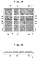
- FIG 2A and FIG 2B are views that illustrate the substrate, in which FIG 2A is a plan view of the substrate and FIG 2B is a side view of the substrate.
- the electronic component 3 includes electronic component-side lands 30.
- the electronic component-side lands 30 face substrate-side lands on the substrate when the electronic component 3 is mounted on the substrate.
- the electronic component-side lands 30 are formed as thin films made of metal, such as copper, having a desired shape by a known method, such as etching and additive process, on a surface of the electronic component 3, facing the substrate.
- FIG 1A and FIG 1B illustrate a case where the plurality of electronic component-side lands 30 having a rectangular planar shape are provided.
- the electronic component-side lands 30 include grounding lands 31 and input/output lands 32.
- the grounding lands 31 are lands for grounding the electronic component 3, and are provided substantially at the center of the surface of the electronic component 3, facing the substrate.
- the input/output lands 32 are lands for inputting or outputting signals between the electronic component 3 and the substrate, and are provided around the grounding lands 31.
- the input/output lands 32 include reinforcement lands 33.
- the reinforcement lands 33 are lands for inputting or outputting signals between the electronic component 3 and the substrate, and for reinforcing connection between the electronic component 3 and the substrate.
- the reinforcement lands 33 are provided near the outer periphery (corner portions in the present embodiment) of the surface of the electronic component 3, facing the substrate.
- the reinforcement lands 33 each have an area larger than those of the other input/output lands 32. Note that the area of each reinforcement land 33 is equal among the reinforcement lands 33. In this way, by providing the reinforcement lands 33 each having an area larger than those of the other input/output lands 32 at the corner portions (four corners in FIG 1B ) of the electronic component 3, occurrence of a fatigue crack/break in solder at soldered portions between the electronic component 3 and the substrate is suppressed to thereby make it possible to improve connection reliability.
- the details of the shapes of these electronic component-side lands 30 will be described later.
- the substrate 2 includes substrate-side lands 20.
- the substrate-side lands 20 are formed as thin films made of metal, such as copper, having a desired shape by a known method, such as etching and additive process, on a surface of the substrate 2, facing the electronic component 3.
- FIG 2A and FIG 2B illustrate a case where the plurality of substrate-side lands 20 having a rectangular planar shape are provided. These substrate-side lands 20 and electronic component-side lands 30 facing the substrate-side lands 20 are placed in pairs at respective arrangement positions. The details of the shape of each substrate-side land 20 will be described later.
- each electronic component-side land 30 and the shape of each substrate-side land 20 will be described.
- the shape of each electronic component-side land 30 other than the reinforcement land 33 (that is, the grounding land 31 and the input/output land 32 other than the reinforcement land 33) is formed to be substantially the same as the shape of each substrate-side land 20 facing the corresponding electronic component-side land 30 (that is, the substrate-side land 20 that is paired with the corresponding electronic component-side land 30).
- each reinforcement land 33 in order to vary the shape of each substrate-side land 20 from the shape of each reinforcement land 33 facing the substrate-side land 20, a groove 34 that serves as a non-soldered region is provided on the surface of each reinforcement land 33, facing the substrate-side land 20.
- the "non-soldered region” means a region on a land to which solder does not adhere.
- a non-soldered region may be physically formed by providing a groove in a land or a non-soldered region may be formed by providing a solder resist layer on a land.
- each reinforcement land 33 is divided by the groove 34, and the planar shape of each reinforcement land 33 divided by the groove 34 is different from the planar shape of the substrate-side land 20 at the position facing the reinforcement land 33.
- the reinforcement land 33 surrounded by the dotted line P in FIG 1B faces the substrate-side land 20 surrounded by the dotted line R in FIG 2A .
- the reinforcement land 33 surrounded by the dotted line P in FIG 1B is divided by the groove 34; whereas the substrate-side land 20 at the position facing the reinforcement land 33 (the substrate-side land 20 surrounded by the dotted line R in FIG 2A ) is not divided by a groove, so the planar shape of the reinforcement land 33 is different from the planar shape of the substrate-side land 20 facing the reinforcement land 33.
- the reinforcement land 33 surrounded by the dotted line Q in FIG 1B is divided by the groove 34; whereas the substrate-side land 20 at the position facing the reinforcement land 33 (the substrate-side land 20 surrounded by the dotted line S in FIG 2A ) is not divided by a groove, so the planar shape of the reinforcement land 33 is different from the planar shape of the substrate-side land 20 facing the reinforcement land 33.
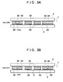
- FIG 3A and FIG 3B are views that show a state where the electronic component 3 is mounted on the substrate 2, in which FIG 3A is a side cross-sectional view that illustrates a state where solder is supplied between each electronic component-side land 30 and a corresponding one of the substrate-side lands 20, and FIG 3B is a side cross-sectional view that illustrates a state after the electronic component 3 is mounted on the substrate 2.
- FIG 3A and FIG 3B show the III-III cross-sectional views of the electronic component 3 illustrated in FIG 1B and the substrate 2 illustrated in FIG 2A .
- voids may be generated in solder between each substrate-side land 20 and a corresponding one of the electronic component-side lands 30 having a relatively large area among the electronic component-side lands 30 (for example, the reinforcement lands 33 that have the largest area among the plurality of electronic component-side lands 30 provided near the outer periphery of the surface of the electronic component 3, facing the substrate 2, and the electronic component-side land 30 having the largest area among all the electronic component-side lands 30).
- the reinforcement land such voids are enclosed by the reinforcement land, the substrate-side land and the surrounding solder and remain in the soldered portion after solder is cooled, so the soldered area between the electronic component and the substrate reduces.
- the groove 34 is provided on the surface of each reinforcement land 33, facing the substrate-side land 20, so gas in the generated voids is emitted outside the soldered portion via a gap formed between each groove 34 and the corresponding substrate-side land 20.
- a space between each reinforcement land 33 and the corresponding substrate-side land 20 is filled with solder except a V-shaped gap portion formed between the position of the groove 34 of the reinforcement land 33 and the substrate-side land 20.
- each of the surface of each electronic component-side land 30, facing the corresponding substrate-side land 20, and the surface of each substrate-side land 20, facing the corresponding electronic component-side land 30, has a groove and then each of these electronic component-side land 30 and substrate-side land 20 is completely divided by the groove so that the shape of each substrate-side land 20 is the same as the shape of the corresponding electronic component-side land 30 facing the substrate-side land 20, for example, as in the case of the portion C in FIG 3B , solder does not flow between the groove of each electronic component-side land 30 and the groove of the corresponding substrate-side land 20.
- a gap having a rectangular cross section is formed between the groove of each electronic component-side land 30 and the groove of the corresponding substrate-side land 20. Therefore, the soldered area between the electronic component 3 and the substrate 2 reduces.
- each reinforcement land 33 is divided by the groove 34.
- the planar shape of each reinforcement land 33 is different from the planar shape of the substrate-side land 20 at the position facing the electronic component-side land. Therefore, no solder flows to the positions of the grooves 34 of the reinforcement lands 33; however, solder flows to the surfaces of the substrate-side lands 20.
- a V-shaped gap is formed between the groove 34 of the reinforcement land 33 and the corresponding substrate-side land 20.
- the groove 34 is provided on the surface of each reinforcement land 33, facing the corresponding substrate-side land 20, so that the shape of each substrate-side land 20 is different from the shape of the corresponding reinforcement land 33 facing the substrate-side land 20, so gas in the generated voids may be emitted outside the soldered portion via the gap formed between each groove 34 and the corresponding substrate-side land 20.
- the groove 34 is provided for each electronic component-side land 30 having the largest area (each reinforcement land 33 in the present embodiment) among the plurality of electronic component-side lands 30.
- each electronic component-side land 30 having the largest area (each reinforcement land 33 in the present embodiment) among the plurality of electronic component-side lands 30 provided near the outer periphery of the surface of the electronic component 3, facing the substrate 2.
- each reinforcement land 33 divided by the groove 34 is different from the planar shape of the substrate-side land 20 at the position facing the reinforcement land 33, so a V-shaped gap is formed between the groove 34 of each reinforcement land 33 and the corresponding substrate-side land 20.
- the groove 34 is provided on the surface of each reinforcement land 33, facing the corresponding substrate-side land 20, as the non-soldered region, so gas in the generated voids may be emitted outside the soldered portion via the gap formed between each groove 34 and the corresponding substrate-side land 20.
- each reinforcement land 33 is divided by the groove 34 and thus the planar shape of each reinforcement land 33 divided by the groove 34 is different from the planar shape of the substrate-side land 20 at the position facing the reinforcement land 33; instead, the thickness of the reinforcement land 33 at the position of the groove 34 may be different from the thickness of the substrate-side land 20 at the position facing the groove 34.
- FIG 4A and FIG 4B are views that show a state where an electronic component 3 is mounted on a substrate 2 according to an alternative embodiment, in which FIG 4A is a side cross-sectional view that illustrates a state where solder is supplied between each electronic component-side land 30 and a corresponding substrate-side land 20, and FIG 4B is a side cross-sectional view that illustrates a state after the electronic component 3 is mounted on the substrate 2.
- each reinforcement land 33 is divided by a groove 34, and, in addition, each substrate-side land 20 also has a groove 21 at the position facing the groove 34 of the reinforcement land 33.
- each reinforcement land 33 at the position of the groove 34 of the reinforcement land 33 is 0, that is, each reinforcement land 33 is completely divided by the groove 34; whereas the thickness of each substrate-side land 20 at the position of the groove 34 (that is, the position of the groove 21 of the substrate-side land 20) is set to a predetermined thickness larger than 0.
- the groove 21 of each substrate-side land 20 is provided so as to be open toward the surface of the substrate-side land 20, facing the reinforcement land 33.
- a V-shaped gap is formed between the groove 34 of each reinforcement land 33 and the groove 21 of the corresponding substrate-side land 20.
- each substrate-side land 20 may also be divided by a groove 21.
- FIG 5 is a plan view of an electronic component 3 when each substrate-side land 20 is also divided by the groove 21.
- FIG 6 is a plan view of a substrate 2 when each substrate-side land 20 is also divided by the groove 21.
- FIG 7A and FIG 7B are views that illustrate a case where each substrate-side land 20 is also divided by the groove 21, in which FIG 7A is a side cross-sectional view that illustrates a state where solder is supplied between each electronic component-side land 30 and a corresponding substrate-side land 20, and FIG 7B is a side cross-sectional view that illustrates a state after the electronic component 3 is mounted on the substrate 2.
- FIG 7A shows the VIIA-VIIA cross-sectional views of the electronic component 3 illustrated in FIG 5 and the substrate 2 illustrated in FIG 6
- FIG 7B shows the VIIB-VIIB cross-sectional views of the electronic component 3 illustrated in FIG 5 and the substrate 2 illustrated in FIG 6 .
- the reinforcement lands 33 and the substrate-side lands 20 are formed so that the groove 34 of each reinforcement land 33 intersects with the groove 21 of the corresponding substrate-side land 20 facing the reinforcement land 33.
- a space between each reinforcement land 33 and the corresponding substrate-side land 20 is filled with solder except the V-shaped gap portion formed between the position of the groove 34 of the reinforcement land 33 and the substrate-side land 20 and the V-shaped gap portion formed between the reinforcement land 33 and the position of the groove 21 of the substrate-side land 20.
- gas in the generated voids may be emitted outside the soldered portion via the gap formed between the groove 34 of the reinforcement land 33 and the substrate-side land 20 and the gap formed between the groove 21 of the substrate-side land 20 and the electronic component-side land 30, so it is possible to further reliably reduce residual voids while stably ensuring the appropriate soldered area between the electronic component 3 and the substrate 2.
- no groove is provided for each substrate-side land 20 and only each reinforcement land 33 is divided by the groove 34; instead, only each substrate-side land 20 facing the reinforcement land 33 may be divided by a groove and no groove may be provided for each reinforcement land 33.
- gas in the generated voids may be emitted outside the soldered portion via the gap formed between the groove of the substrate-side land 20 and the corresponding electronic component-side land 30.
- the groove 34 is provided for each reinforcement land 33; instead, not only the reinforcement land 33 but also the other electronic component-side land 30 each may have a groove.
- a groove may be provided for all the electronic component-side lands 30 or a groove may be provided for only part of the electronic component-side lands 30.
- only one groove 34 is provided for each reinforcement land 33; instead, a plurality of the grooves 34 may be provided for each reinforcement land 33.
- two grooves 34 may be provided for each reinforcement land 33 so as to intersect with each other.
- a V-shaped gap is formed between the groove 34 of each reinforcement land 33 and the corresponding substrate-side land 20; however, the shape of the gap formed is not limited to the V shape.
- the shape of the gap formed may be another shape, such as a U shape.
- the reinforcement land 33 is provided at each corner portion of the surface of the electronic component 3, facing the substrate; instead, the reinforcement land 33 may be provided at a selected position near the outer periphery of the surface of the electronic component 3, facing the substrate (for example, at predetermined intervals over all around the outer periphery).
- the groove 34 is provided on the surface of the electronic component-side land 30, facing the substrate-side land 20, as the non-soldered regions; instead, a solder resist layer may be provided on the surface of the electronic component-side land 30, facing the substrate-side land 20, as a non-soldered region.
- a solder resist layer may be provided on the surface of the electronic component-side land 30, facing the substrate-side land 20, as a non-soldered region.
- FIG 8 is a side cross-sectional view that illustrates a state after the electronic component 3 is mounted on the substrate 2.
- a solder resist layer may be provided on the surface of the substrate-side land 20, facing the electronic component-side land 30.
- gas in the generated voids may be emitted outside the soldered portion via the gap formed between the solder resist layer and the electronic component-side land 30.
- An electronic component to be mounted on a substrate comprises an electronic component-side land that faces a substrate-side land provided on the substrate when the electronic component is mounted on the substrate.
- a non-soldered region is provided on a surface of the electronic component-side land, facing the substrate-side land, so that a shape of the substrate-side land is different from a shape of the electronic component-side land facing the substrate-side land.
Landscapes
- Electric Connection Of Electric Components To Printed Circuits (AREA)
- Structures For Mounting Electric Components On Printed Circuit Boards (AREA)
Abstract
Description
- The disclosure of Japanese Patent Application No.
2010-241338 filed on October 27, 2010 - The present invention relates to an electronic component and an electronic device.
- In an existing art, soldering copper foils (hereinafter, referred to as "lands") for mounting an electronic component on a substrate are provided on the substrate and the electronic component. Particularly, in recent years, in order to reduce the footprint of an electronic component on a substrate, packaging, such as ball grid array (BGA) and land grid array (LGA), is utilized to provide lands directly below the electronic component.
- In an electronic component soldered to a substrate via lands in this way, in order to improve the reliability of connection of connecting land portions, there has been suggested a module component in which reinforcement lands having an area that is three times or more of the area of one connecting land is provided near the outermost periphery of connecting lands that are arranged in a grid on the back surface of a module substrate (for example, see Japanese Patent No.
2859143 - There is a possibility that voids are generated in a soldered portion because of the surface tension of solder, gas generated from an electronic component or a base material during reflowing, or the like. Particularly, if lands having a large area are provided as in the case of the above described existing component, there is a possibility that the frequency of occurrence of voids increases, and the size of each void generated increases. In this way, if excessive amounts of voids are generated in a soldered portion and then the voids remain in the soldered portion, a soldered area between an electronic component and a substrate reduces and may lead to deterioration of electrical characteristic and thermal conductivity.
- The present invention provides an electronic component and an electronic device in which residual voids in a soldered portion is reduced to make it possible to stably ensure an appropriate soldered area between the electronic component and a substrate.
- A first aspect of the invention provides an electronic component to be mounted on a substrate. The electronic component includes: an electronic component-side land that faces a substrate-side land provided on the substrate when the electronic component is mounted on the substrate, wherein a non-soldered region is provided on a surface of the electronic component-side land, facing the substrate-side land, so that a shape of the substrate-side land is different from a shape of the electronic component-side land facing the substrate-side land.
- With the electronic component according to the first aspect, the non-soldered region is provided on the surface of the electronic component-side land, facing the substrate-side land, so that the shape of the substrate-side land is different from the shape of the electronic component-side land facing the substrate-side land, so gas in generated voids may be emitted outside a soldered portion via a gap formed between the non-soldered region and the substrate-side land. By so doing, residual voids in the soldered portion are reduced to thereby make it possible to stably ensure the appropriate soldered area between the electronic component and the substrate.
- A second aspect of the invention provides an electronic component to be mounted on a substrate. The electronic component includes: electronic component-side lands that respectively face substrate-side lands provided on the substrate when the electronic component is mounted on the substrate, wherein the electronic component-side lands include a grounding land that is provided substantially at a center of a surface of the electronic component, facing the substrate, and input/output lands that are provided around the grounding land, the input/output lands include a reinforcement land that is provided near an outer periphery of the surface of the electronic component, facing the substrate, and that is formed to have an area larger than that of the other input/output land, and a non-soldered region is provided on a surface of the reinforcement land, facing the substrate-side land, so that a shape of the substrate-side land is different from a shape of the reinforcement land facing the substrate-side land.
- With the electronic component according to the second aspect, the non-soldered region is provided on the surface of the reinforcement land, facing the substrate-side land, so that the shape of the substrate-side land is different from the shape of the reinforcement land facing the substrate-side land, so gas in generated voids may be emitted outside a soldered portion via a gap formed between the non-soldered region and the substrate-side land. By so doing, residual voids in the soldered portion between the reinforcement land and the substrate-side land, in which voids are particularly easily generated, are reduced to thereby make it possible to stably ensure the appropriate soldered area between the electronic component and the substrate.
- A third aspect of the invention provides an electronic device. The electronic device includes: a substrate that includes a substrate-side land; and an electronic component that includes an electronic component-side land facing the substrate-side land when the electronic component is mounted on the substrate, wherein a non-soldered region is provided on at least one of a surface of the substrate-side land, facing the electronic component-side land, and a surface of the electronic component-side land, facing the substrate-side land, so that a shape of the substrate-side land is different from a shape of the electronic component-side land facing the substrate-side land.
- With the electronic device according to the third aspect, the non-soldered region is provided on at least one of the surface of the substrate-side land, facing the electronic component-side land, and the surface of the electronic component-side land, facing the substrate-side land, so that the shape of the substrate-side land is different from the shape of the electronic component-side land facing the substrate-side land, so gas in generated voids may be emitted outside a soldered portion via a gap formed between the non-soldered region and the substrate-side land. By so doing, residual voids in the soldered portion are reduced to thereby make it possible to stably ensure the appropriate soldered area between the electronic component and the substrate.
- The features, advantages, and technical and industrial significance of this invention will be described below with reference to the accompanying drawings, in which like numerals denote like elements, and wherein:
-
FIG 1A and FIG 1B are views that illustrate an electronic component, in whichFIG 1A is a side view of the electronic component andFIG 1B is a plan view of the electronic component; -
FIG 2A and FIG 2B are views that illustrate a substrate, in whichFIG 2A is a plan view of the substrate andFIG 2B is a side view of the substrate; -
FIG 3A and FIG 3B are views that show a state where the electronic component is mounted on the substrate, in whichFIG 3A is a side cross-sectional view that illustrates a state where solder is supplied between each electronic component-side land and a corresponding substrate-side land, andFIG 3B is a side cross-sectional view that illustrates a state after the electronic component is mounted on the substrate; -
FIG 4A and FIG 4B are views that show a state where an electronic component is mounted on a substrate according to an alternative embodiment, in whichFIG 4A is a side cross-sectional view that illustrates a state where solder is supplied between each electronic component-side land and a corresponding substrate-side land, andFIG 4B is a side cross-sectional view that illustrates a state after the electronic component is mounted on the substrate; -
FIG 5 is a plan view of an electronic component in the case where some electronic component-side lands and some substrate-side lands are divided by grooves; -
FIG 6 is a plan view of a substrate in the case where some electronic component-side lands and some substrate-side lands are divided by grooves; -
FIG 7A and FIG 7B are views that illustrate a case where some electronic component-side lands and some substrate-side lands are divided by grooves, in whichFIG 7A is a side cross-sectional view that illustrates a state where solder is supplied between each electronic component-side land and a corresponding substrate-side land, andFIG 7B is a side cross-sectional view that illustrates a state after the electronic component is mounted on the substrate; and -
FIG 8 is a side cross-sectional view that illustrates a state after the electronic component is mounted on the substrate. - Hereinafter, an embodiment of an electronic component and an electronic device according to the aspect of the present invention will be described in detail with reference to the accompanying drawings. However, the aspect of the present invention is not limited to the embodiment. In addition, in the following description, a "land" means a soldering metal thin film (copper foil, or the like) for mounting an electronic component to a substrate.
- First, the configuration of an electronic device according to the embodiment will be described. The electronic device includes a substrate and an electronic component that is mounted on the substrate.
FIG 1A and FIG 1B are views that illustrate the electronic component, in whichFIG 1A is a side view of the electronic component andFIG 1B is a plan view of the electronic component. In addition,FIG 2A and FIG 2B are views that illustrate the substrate, in whichFIG 2A is a plan view of the substrate andFIG 2B is a side view of the substrate. - The electronic component will be described below. As shown in
FIG 1A and FIG 1B , theelectronic component 3 includes electronic component-side lands 30. The electronic component-side lands 30 face substrate-side lands on the substrate when theelectronic component 3 is mounted on the substrate. The electronic component-side lands 30 are formed as thin films made of metal, such as copper, having a desired shape by a known method, such as etching and additive process, on a surface of theelectronic component 3, facing the substrate.FIG 1A and FIG 1B illustrate a case where the plurality of electronic component-side lands 30 having a rectangular planar shape are provided. - The electronic component-side lands will be described below. The electronic component-
side lands 30 includegrounding lands 31 and input/output lands 32. Thegrounding lands 31 are lands for grounding theelectronic component 3, and are provided substantially at the center of the surface of theelectronic component 3, facing the substrate. The input/output lands 32 are lands for inputting or outputting signals between theelectronic component 3 and the substrate, and are provided around thegrounding lands 31. In addition, the input/output lands 32 includereinforcement lands 33. Thereinforcement lands 33 are lands for inputting or outputting signals between theelectronic component 3 and the substrate, and for reinforcing connection between theelectronic component 3 and the substrate. Thereinforcement lands 33 are provided near the outer periphery (corner portions in the present embodiment) of the surface of theelectronic component 3, facing the substrate. Thereinforcement lands 33 each have an area larger than those of the other input/output lands 32. Note that the area of eachreinforcement land 33 is equal among thereinforcement lands 33. In this way, by providing thereinforcement lands 33 each having an area larger than those of the other input/output lands 32 at the corner portions (four corners inFIG 1B ) of theelectronic component 3, occurrence of a fatigue crack/break in solder at soldered portions between theelectronic component 3 and the substrate is suppressed to thereby make it possible to improve connection reliability. The details of the shapes of these electronic component-side lands 30 will be described later. - The configuration of the substrate will be described below. As shown in
FIG 2A and FIG 2B , thesubstrate 2 includes substrate-side lands 20. The substrate-side lands 20 are formed as thin films made of metal, such as copper, having a desired shape by a known method, such as etching and additive process, on a surface of thesubstrate 2, facing theelectronic component 3.FIG 2A and FIG 2B illustrate a case where the plurality of substrate-side lands 20 having a rectangular planar shape are provided. These substrate-side lands 20 and electronic component-side lands 30 facing the substrate-side lands 20 are placed in pairs at respective arrangement positions. The details of the shape of each substrate-side land 20 will be described later. - Next, the shape of each electronic component-
side land 30 and the shape of each substrate-side land 20 will be described. The shape of each electronic component-side land 30 other than the reinforcement land 33 (that is, the groundingland 31 and the input/output land 32 other than the reinforcement land 33) is formed to be substantially the same as the shape of each substrate-side land 20 facing the corresponding electronic component-side land 30 (that is, the substrate-side land 20 that is paired with the corresponding electronic component-side land 30). - On the other hand, in the reinforcement lands 33, in order to vary the shape of each substrate-
side land 20 from the shape of eachreinforcement land 33 facing the substrate-side land 20, agroove 34 that serves as a non-soldered region is provided on the surface of eachreinforcement land 33, facing the substrate-side land 20. Here, the "non-soldered region" means a region on a land to which solder does not adhere. For example, a non-soldered region may be physically formed by providing a groove in a land or a non-soldered region may be formed by providing a solder resist layer on a land. In the present embodiment, eachreinforcement land 33 is divided by thegroove 34, and the planar shape of eachreinforcement land 33 divided by thegroove 34 is different from the planar shape of the substrate-side land 20 at the position facing thereinforcement land 33. - For example, when the
electronic component 3 is mounted on thesubstrate 2, thereinforcement land 33 surrounded by the dotted line P inFIG 1B faces the substrate-side land 20 surrounded by the dotted line R inFIG 2A . In this case, thereinforcement land 33 surrounded by the dotted line P inFIG 1B is divided by thegroove 34; whereas the substrate-side land 20 at the position facing the reinforcement land 33 (the substrate-side land 20 surrounded by the dotted line R inFIG 2A ) is not divided by a groove, so the planar shape of thereinforcement land 33 is different from the planar shape of the substrate-side land 20 facing thereinforcement land 33. Similarly, thereinforcement land 33 surrounded by the dotted line Q inFIG 1B is divided by thegroove 34; whereas the substrate-side land 20 at the position facing the reinforcement land 33 (the substrate-side land 20 surrounded by the dotted line S inFIG 2A ) is not divided by a groove, so the planar shape of thereinforcement land 33 is different from the planar shape of the substrate-side land 20 facing thereinforcement land 33. - Next, the function of the thus configured
electronic component 3 and electronic device will be described.FIG 3A and FIG 3B are views that show a state where theelectronic component 3 is mounted on thesubstrate 2, in whichFIG 3A is a side cross-sectional view that illustrates a state where solder is supplied between each electronic component-side land 30 and a corresponding one of the substrate-side lands 20, andFIG 3B is a side cross-sectional view that illustrates a state after theelectronic component 3 is mounted on thesubstrate 2. Note thatFIG 3A and FIG 3B show the III-III cross-sectional views of theelectronic component 3 illustrated inFIG 1B and thesubstrate 2 illustrated inFIG 2A . - For example, when solder is supplied between each electronic component-
side land 30 and a corresponding one of the substrate-side lands 20 by a known soldering method, such as reflow soldering, as illustrated inFIG 3A , voids may be generated in solder between each substrate-side land 20 and a corresponding one of the electronic component-side lands 30 having a relatively large area among the electronic component-side lands 30 (for example, the reinforcement lands 33 that have the largest area among the plurality of electronic component-side lands 30 provided near the outer periphery of the surface of theelectronic component 3, facing thesubstrate 2, and the electronic component-side land 30 having the largest area among all the electronic component-side lands 30). In the case of the existing electronic component, such voids are enclosed by the reinforcement land, the substrate-side land and the surrounding solder and remain in the soldered portion after solder is cooled, so the soldered area between the electronic component and the substrate reduces. - In contrast, in the present embodiment, the
groove 34 is provided on the surface of eachreinforcement land 33, facing the substrate-side land 20, so gas in the generated voids is emitted outside the soldered portion via a gap formed between eachgroove 34 and the corresponding substrate-side land 20. As a result, as shown inFIG 3B , a space between eachreinforcement land 33 and the corresponding substrate-side land 20 is filled with solder except a V-shaped gap portion formed between the position of thegroove 34 of thereinforcement land 33 and the substrate-side land 20. By so doing, in comparison with the case where voids remain in the soldered portions, it is possible to ensure the sufficient soldered area between theelectronic component 3 and thesubstrate 2. - In addition, when each of the surface of each electronic component-
side land 30, facing the corresponding substrate-side land 20, and the surface of each substrate-side land 20, facing the corresponding electronic component-side land 30, has a groove and then each of these electronic component-side land 30 and substrate-side land 20 is completely divided by the groove so that the shape of each substrate-side land 20 is the same as the shape of the corresponding electronic component-side land 30 facing the substrate-side land 20, for example, as in the case of the portion C inFIG 3B , solder does not flow between the groove of each electronic component-side land 30 and the groove of the corresponding substrate-side land 20. Thus, a gap having a rectangular cross section is formed between the groove of each electronic component-side land 30 and the groove of the corresponding substrate-side land 20. Therefore, the soldered area between theelectronic component 3 and thesubstrate 2 reduces. - In contrast, in the present embodiment, no groove is provided for each substrate-
side land 20, and only eachreinforcement land 33 is divided by thegroove 34. By so doing, the planar shape of eachreinforcement land 33 is different from the planar shape of the substrate-side land 20 at the position facing the electronic component-side land. Therefore, no solder flows to the positions of thegrooves 34 of the reinforcement lands 33; however, solder flows to the surfaces of the substrate-side lands 20. By so doing, as shown inFIG 3B , a V-shaped gap is formed between thegroove 34 of thereinforcement land 33 and the corresponding substrate-side land 20. Thus, in comparison with the state where a gap having a rectangular cross section is formed between the groove of eachreinforcement land 33 and the groove of the corresponding substrate-side land 20, the sufficient soldered area between theelectronic component 3 and thesubstrate 2 may be ensured. - In this way, according to the present embodiment, the
groove 34 is provided on the surface of eachreinforcement land 33, facing the corresponding substrate-side land 20, so that the shape of each substrate-side land 20 is different from the shape of the correspondingreinforcement land 33 facing the substrate-side land 20, so gas in the generated voids may be emitted outside the soldered portion via the gap formed between eachgroove 34 and the corresponding substrate-side land 20. By so doing, residual voids in the soldered portions are reduced to thereby make it possible to stably ensure the appropriate soldered area between theelectronic component 3 and thesubstrate 2. - Particularly, the
groove 34 is provided for each electronic component-side land 30 having the largest area (eachreinforcement land 33 in the present embodiment) among the plurality of electronic component-side lands 30. By so doing, residual voids in the soldered portion between eachreinforcement land 33 and the corresponding substrate-side land 20, in which voids are particularly easily generated, are reduced to thereby make it possible to stably ensure the appropriate soldered area between theelectronic component 3 and thesubstrate 2. - In addition, the
groove 34 is provided for each electronic component-side land 30 having the largest area (eachreinforcement land 33 in the present embodiment) among the plurality of electronic component-side lands 30 provided near the outer periphery of the surface of theelectronic component 3, facing thesubstrate 2. By so doing, residual voids in the soldered portion between eachreinforcement land 33 and the corresponding substrate-side land 20, in which voids are particularly easily generated, are reduced to thereby make it possible to stably ensure the appropriate soldered area between theelectronic component 3 and thesubstrate 2. - In addition, the planar shape of each
reinforcement land 33 divided by thegroove 34 is different from the planar shape of the substrate-side land 20 at the position facing thereinforcement land 33, so a V-shaped gap is formed between thegroove 34 of eachreinforcement land 33 and the corresponding substrate-side land 20. By so doing, in addition to the above described basic advantageous effects, it is possible to ensure the sufficient soldered area between theelectronic component 3 and thesubstrate 2 in comparison with a state where a gap having a rectangular cross section is formed between the groove of eachreinforcement land 33 and the groove of the corresponding substrate-side land 20. - In addition, the
groove 34 is provided on the surface of eachreinforcement land 33, facing the corresponding substrate-side land 20, as the non-soldered region, so gas in the generated voids may be emitted outside the soldered portion via the gap formed between eachgroove 34 and the corresponding substrate-side land 20. - The embodiment according to the aspect of the invention is described above; however, the specific configuration and manner according to the aspect of the invention may be arbitrarily modified or improved within the scope of the technical ideas recited in the appended claims. Hereinafter, such alternative embodiments will be described.
- First, problems to be solved by the aspect of the invention and the advantageous effects of the aspect of the invention are not limited to the above described ones; they may vary depending on an environment in which the aspect of the invention is implemented or the details of the configuration, and only part of the above described problems may be solved or only part of the above described advantageous effects may be obtained.
- In the above described embodiment, each
reinforcement land 33 is divided by thegroove 34 and thus the planar shape of eachreinforcement land 33 divided by thegroove 34 is different from the planar shape of the substrate-side land 20 at the position facing thereinforcement land 33; instead, the thickness of thereinforcement land 33 at the position of thegroove 34 may be different from the thickness of the substrate-side land 20 at the position facing thegroove 34.FIG 4A and FIG 4B are views that show a state where anelectronic component 3 is mounted on asubstrate 2 according to an alternative embodiment, in whichFIG 4A is a side cross-sectional view that illustrates a state where solder is supplied between each electronic component-side land 30 and a corresponding substrate-side land 20, andFIG 4B is a side cross-sectional view that illustrates a state after theelectronic component 3 is mounted on thesubstrate 2. In the example ofFIG 4A and FIG 4B , as well as the above described embodiment, eachreinforcement land 33 is divided by agroove 34, and, in addition, each substrate-side land 20 also has agroove 21 at the position facing thegroove 34 of thereinforcement land 33. However, the thickness of eachreinforcement land 33 at the position of thegroove 34 of thereinforcement land 33 is 0, that is, eachreinforcement land 33 is completely divided by thegroove 34; whereas the thickness of each substrate-side land 20 at the position of the groove 34 (that is, the position of thegroove 21 of the substrate-side land 20) is set to a predetermined thickness larger than 0. Note that thegroove 21 of each substrate-side land 20 is provided so as to be open toward the surface of the substrate-side land 20, facing thereinforcement land 33. When solder is supplied between the thus configuredreinforcement land 33 and substrate-side land 20, no solder flows to the position of thegroove 34 of the completely dividedreinforcement land 33; however, solder flows to the surface of the substrate-side land 20 that is not completely divided, including the position of thegroove 21. By so doing, as shown inFIG 4B , a V-shaped gap is formed between thegroove 34 of eachreinforcement land 33 and thegroove 21 of the corresponding substrate-side land 20. Thus, in comparison with a state where a gap having a rectangular cross section is formed between the groove of eachreinforcement land 33 and the groove of the corresponding substrate-side land 20, it is possible to ensure the sufficient soldered area between theelectronic component 3 and thesubstrate 2. - In addition, in the above described embodiment, no groove is provided for each substrate-
side land 20 and only eachreinforcement land 33 is divided by thegroove 34; instead, in addition to each reinforcement land 33 (electronic component-side land 30), each substrate-side land 20 may also be divided by agroove 21.FIG 5 is a plan view of anelectronic component 3 when each substrate-side land 20 is also divided by thegroove 21.FIG 6 is a plan view of asubstrate 2 when each substrate-side land 20 is also divided by thegroove 21.FIG 7A and FIG 7B are views that illustrate a case where each substrate-side land 20 is also divided by thegroove 21, in whichFIG 7A is a side cross-sectional view that illustrates a state where solder is supplied between each electronic component-side land 30 and a corresponding substrate-side land 20, andFIG 7B is a side cross-sectional view that illustrates a state after theelectronic component 3 is mounted on thesubstrate 2. Note thatFIG 7A shows the VIIA-VIIA cross-sectional views of theelectronic component 3 illustrated inFIG 5 and thesubstrate 2 illustrated inFIG 6 , andFIG 7B shows the VIIB-VIIB cross-sectional views of theelectronic component 3 illustrated inFIG 5 and thesubstrate 2 illustrated inFIG 6 . - In the example shown in
FIG 5 to FIG 7B , when theelectronic component 3 is mounted on thesubstrate 2, the reinforcement lands 33 and the substrate-side lands 20 are formed so that thegroove 34 of eachreinforcement land 33 intersects with thegroove 21 of the corresponding substrate-side land 20 facing thereinforcement land 33. In this case, as shown inFIG 7A and FIG 7B , a space between eachreinforcement land 33 and the corresponding substrate-side land 20 is filled with solder except the V-shaped gap portion formed between the position of thegroove 34 of thereinforcement land 33 and the substrate-side land 20 and the V-shaped gap portion formed between thereinforcement land 33 and the position of thegroove 21 of the substrate-side land 20. By so doing, gas in the generated voids may be emitted outside the soldered portion via the gap formed between thegroove 34 of thereinforcement land 33 and the substrate-side land 20 and the gap formed between thegroove 21 of the substrate-side land 20 and the electronic component-side land 30, so it is possible to further reliably reduce residual voids while stably ensuring the appropriate soldered area between theelectronic component 3 and thesubstrate 2. - In addition, in the above described embodiment, no groove is provided for each substrate-
side land 20 and only eachreinforcement land 33 is divided by thegroove 34; instead, only each substrate-side land 20 facing thereinforcement land 33 may be divided by a groove and no groove may be provided for eachreinforcement land 33. In this case as well, gas in the generated voids may be emitted outside the soldered portion via the gap formed between the groove of the substrate-side land 20 and the corresponding electronic component-side land 30. By so doing, residual voids in the soldered portions are reduced to thereby make it possible to stably ensure the appropriate soldered area between theelectronic component 3 and thesubstrate 2. - In addition, in the above described embodiment, the
groove 34 is provided for eachreinforcement land 33; instead, not only thereinforcement land 33 but also the other electronic component-side land 30 each may have a groove. In this case, a groove may be provided for all the electronic component-side lands 30 or a groove may be provided for only part of the electronic component-side lands 30. - In addition, in the above described embodiment, only one
groove 34 is provided for eachreinforcement land 33; instead, a plurality of thegrooves 34 may be provided for eachreinforcement land 33. For example, twogrooves 34 may be provided for eachreinforcement land 33 so as to intersect with each other. By so doing, it is possible to further effectively reduce residual voids in the soldered portions. - In addition, in the above described embodiment, a V-shaped gap is formed between the
groove 34 of eachreinforcement land 33 and the corresponding substrate-side land 20; however, the shape of the gap formed is not limited to the V shape. The shape of the gap formed may be another shape, such as a U shape. - In addition, in the above described embodiment, the
reinforcement land 33 is provided at each corner portion of the surface of theelectronic component 3, facing the substrate; instead, thereinforcement land 33 may be provided at a selected position near the outer periphery of the surface of theelectronic component 3, facing the substrate (for example, at predetermined intervals over all around the outer periphery). - In addition, in the above described embodiment, the
groove 34 is provided on the surface of the electronic component-side land 30, facing the substrate-side land 20, as the non-soldered regions; instead, a solder resist layer may be provided on the surface of the electronic component-side land 30, facing the substrate-side land 20, as a non-soldered region. In this way, by providing the solder resist layer on the electronic component-side land 30, the shape of the soldered portion of the substrate-side land 20 is different from the shape of the soldered portion of the electronic component-side land 30 facing the substrate-side land 20. That is, in view of the function of the land that is connected by solder, the shape of the substrate-side land 20 is different from the shape of the electronic component-side land 30 facing the substrate-side land 20. - For example, a solder resist layer is formed in a band shape on the surface of each
reinforcement land 33, facing the substrate-side land 20, to divide thereinforcement land 33 with the solder resist layer. By so doing, the planar shape of thereinforcement land 33 divided by the solder resist layer is different from the planar shape of the substrate-side land 20 at the position facing thereinforcement land 33.FIG 8 is a side cross-sectional view that illustrates a state after theelectronic component 3 is mounted on thesubstrate 2. In this case, when solder is supplied between each electronic component-side land 30 and the corresponding substrate-side land 20, no solder adheres to the solder resist layer, so, as shown inFIG 8 , a V-shaped gap portion is formed between the position of the solder resist layer of eachreinforcement land 33 and the corresponding substrate-side land 20. In this way, by providing the solder resist layer on the surface of the electronic component-side land 30, facing the substrate-side land 20, as a non-soldered region, a non-soldered region may be easily formed on the electronic component-side land 30, and gas in the generated voids may be emitted outside the soldered portion via the gap formed between the solder resist layer and the substrate-side land 20. - In addition, a solder resist layer may be provided on the surface of the substrate-
side land 20, facing the electronic component-side land 30. In this case as well, gas in the generated voids may be emitted outside the soldered portion via the gap formed between the solder resist layer and the electronic component-side land 30.
An electronic component to be mounted on a substrate comprises an electronic component-side land that faces a substrate-side land provided on the substrate when the electronic component is mounted on the substrate. A non-soldered region is provided on a surface of the electronic component-side land, facing the substrate-side land, so that a shape of the substrate-side land is different from a shape of the electronic component-side land facing the substrate-side land.
Claims (9)
- An electronic component to be mounted on a substrate, comprising:an electronic component-side land that faces a substrate-side land provided on the substrate when the electronic component is mounted on the substrate, whereina non-soldered region is provided on a surface of the electronic component-side land, facing the substrate-side land, so that a shape of the substrate-side land is different from a shape of the electronic component-side land facing the substrate-side land.
- The electronic component according to claim 1, wherein
a plurality of the electronic component-side lands are provided, and
the non-soldered region is provided on the electronic component-side land having the largest area among the plurality of electronic component-side lands. - The electronic component according to claim 2, wherein
the plurality of electronic component-side lands are provided near an outer periphery of a surface of the electronic component, facing the substrate, and
the non-soldered region is provided on the electronic component-side land having the largest area among the plurality of electronic component-side lands provided near the outer periphery of the surface of the electronic component, facing the substrate. - The electronic component according to claim 1, wherein
the electronic component-side land is divided by the non-soldered region, and
a planar shape of the electronic component-side land divided by the non-soldered region is different from a planar shape of the substrate-side land at a position facing the divided electronic component-side land. - The electronic component according to claim 1, wherein
a groove is provided on the surface of the electronic component-side land, facing the substrate-side land, as the non-soldered region. - The electronic component according to claim 5, wherein
a thickness of the electronic component-side land at a position of the groove is different from a thickness of the substrate-side land at a position facing the groove. - The electronic component according to claim 1, wherein
a solder resist layer is provided on the surface of the electronic component-side land, facing the substrate-side land, as the non-soldered region. - An electronic component to be mounted on a substrate, comprising:electronic component-side lands that respectively face substrate-side lands provided on the substrate when the electronic component is mounted on the substrate, whereinthe electronic component-side lands include a grounding land that is provided substantially at a center of a surface of the electronic component, facing the substrate, and input/output lands that are provided around the grounding land,the input/output lands include a reinforcement land that is provided near an outer periphery of the surface of the electronic component, facing the substrate, and that is formed to have an area larger than that of the other input/output land, anda non-soldered region is provided on a surface of the reinforcement land, facing the substrate-side land, so that a shape of the substrate-side land is different from a shape of the reinforcement land facing the substrate-side land.
- An electronic device comprising:a substrate that includes a substrate-side land; andan electronic component that includes an electronic component-side land facing the substrate-side land when the electronic component is mounted on the substrate, whereina non-soldered region is provided on at least one of a surface of the substrate-side land, facing the electronic component-side land, and a surface of the electronic component-side land, facing the substrate-side land, so that a shape of the substrate-side land is different from a shape of the electronic component-side land facing the substrate-side land.
Applications Claiming Priority (1)
| Application Number | Priority Date | Filing Date | Title |
|---|---|---|---|
| JP2010241338A JP5581972B2 (en) | 2010-10-27 | 2010-10-27 | Electronic component and electronic device |
Publications (2)
| Publication Number | Publication Date |
|---|---|
| EP2447994A2 true EP2447994A2 (en) | 2012-05-02 |
| EP2447994A3 EP2447994A3 (en) | 2018-01-24 |
Family
ID=44785358
Family Applications (1)
| Application Number | Title | Priority Date | Filing Date |
|---|---|---|---|
| EP11180886.1A Withdrawn EP2447994A3 (en) | 2010-10-27 | 2011-09-12 | Electronic component and electronic device |
Country Status (4)
| Country | Link |
|---|---|
| US (1) | US8787033B2 (en) |
| EP (1) | EP2447994A3 (en) |
| JP (1) | JP5581972B2 (en) |
| CN (1) | CN102458048B (en) |
Cited By (1)
| Publication number | Priority date | Publication date | Assignee | Title |
|---|---|---|---|---|
| WO2021225860A1 (en) | 2020-05-07 | 2021-11-11 | Wolfspeed, Inc. | Packaged transistor with channeled die attach materials and process of implementing the same |
Families Citing this family (4)
| Publication number | Priority date | Publication date | Assignee | Title |
|---|---|---|---|---|
| ITMI20111776A1 (en) * | 2011-09-30 | 2013-03-31 | St Microelectronics Srl | ELECTRONIC SYSTEM FOR REFLOW SOLDERING |
| DE102012105297A1 (en) * | 2012-06-19 | 2013-12-19 | Endress + Hauser Gmbh + Co. Kg | Method for connecting a component to a carrier via a soldering and component for connecting to a carrier |
| JP6504762B2 (en) | 2014-08-05 | 2019-04-24 | キヤノン株式会社 | Module manufacturing method |
| US10177107B2 (en) * | 2016-08-01 | 2019-01-08 | Xilinx, Inc. | Heterogeneous ball pattern package |
Citations (2)
| Publication number | Priority date | Publication date | Assignee | Title |
|---|---|---|---|---|
| JP2859143B2 (en) | 1994-11-08 | 1999-02-17 | 松下電器産業株式会社 | Module parts |
| JP2010241338A (en) | 2009-04-08 | 2010-10-28 | Denso Corp | Vehicle control apparatus and vehicle control program |
Family Cites Families (16)
| Publication number | Priority date | Publication date | Assignee | Title |
|---|---|---|---|---|
| US3599326A (en) * | 1969-01-27 | 1971-08-17 | Philco Ford Corp | Method of forming electrical connections with solder resistant surfaces |
| JPS607758A (en) * | 1983-06-27 | 1985-01-16 | Nec Corp | Semiconductor device |
| US7654432B2 (en) * | 1997-05-27 | 2010-02-02 | Wstp, Llc | Forming solder balls on substrates |
| US6169253B1 (en) * | 1998-06-08 | 2001-01-02 | Visteon Global Technologies, Inc. | Solder resist window configurations for solder paste overprinting |
| US6267009B1 (en) * | 1998-12-14 | 2001-07-31 | Endress + Hauser Gmbh + Co. | Capacitive pressure sensor cells or differential pressure sensor cells and methods for manufacturing the same |
| US7034402B1 (en) * | 2000-06-28 | 2006-04-25 | Intel Corporation | Device with segmented ball limiting metallurgy |
| JP2004095867A (en) * | 2002-08-30 | 2004-03-25 | Casio Comput Co Ltd | Electronic components |
| JP2005223090A (en) * | 2004-02-04 | 2005-08-18 | Murata Mfg Co Ltd | Connection structure between mounting board and components |
| JP2006060141A (en) * | 2004-08-23 | 2006-03-02 | Sharp Corp | Printed circuit board and mounting method of surface mount semiconductor package using the same |
| US7892972B2 (en) * | 2006-02-03 | 2011-02-22 | Micron Technology, Inc. | Methods for fabricating and filling conductive vias and conductive vias so formed |
| US20080003803A1 (en) * | 2006-06-30 | 2008-01-03 | Pei-Haw Tsao | Semiconductor package substrate for flip chip packaging |
| US20080142964A1 (en) * | 2006-12-13 | 2008-06-19 | Haixiao Sun | Tubular-shaped bumps for integrated circuit devices and methods of fabrication |
| US20080150101A1 (en) * | 2006-12-20 | 2008-06-26 | Tessera, Inc. | Microelectronic packages having improved input/output connections and methods therefor |
| JP2008227271A (en) * | 2007-03-14 | 2008-09-25 | Fujitsu Ltd | Electronic device and electronic component mounting method |
| US7667335B2 (en) * | 2007-09-20 | 2010-02-23 | Stats Chippac, Ltd. | Semiconductor package with passivation island for reducing stress on solder bumps |
| JP4999806B2 (en) * | 2008-09-18 | 2012-08-15 | アルプス電気株式会社 | Electronic module and manufacturing method thereof |
-
2010
- 2010-10-27 JP JP2010241338A patent/JP5581972B2/en not_active Expired - Fee Related
-
2011
- 2011-09-12 EP EP11180886.1A patent/EP2447994A3/en not_active Withdrawn
- 2011-09-16 US US13/235,111 patent/US8787033B2/en not_active Expired - Fee Related
- 2011-10-18 CN CN201110319259.9A patent/CN102458048B/en not_active Expired - Fee Related
Patent Citations (2)
| Publication number | Priority date | Publication date | Assignee | Title |
|---|---|---|---|---|
| JP2859143B2 (en) | 1994-11-08 | 1999-02-17 | 松下電器産業株式会社 | Module parts |
| JP2010241338A (en) | 2009-04-08 | 2010-10-28 | Denso Corp | Vehicle control apparatus and vehicle control program |
Cited By (2)
| Publication number | Priority date | Publication date | Assignee | Title |
|---|---|---|---|---|
| WO2021225860A1 (en) | 2020-05-07 | 2021-11-11 | Wolfspeed, Inc. | Packaged transistor with channeled die attach materials and process of implementing the same |
| EP4139955A4 (en) * | 2020-05-07 | 2024-06-05 | Wolfspeed, Inc. | ENCAPSULATED TRANSISTOR HAVING CHANNELED CHIP ATTACHMENT MATERIALS AND METHOD FOR IMPLEMENTING SAME |
Also Published As
| Publication number | Publication date |
|---|---|
| EP2447994A3 (en) | 2018-01-24 |
| CN102458048B (en) | 2015-10-21 |
| CN102458048A (en) | 2012-05-16 |
| US8787033B2 (en) | 2014-07-22 |
| JP5581972B2 (en) | 2014-09-03 |
| JP2012094712A (en) | 2012-05-17 |
| US20120106116A1 (en) | 2012-05-03 |
Similar Documents
| Publication | Publication Date | Title |
|---|---|---|
| CN111699552B (en) | High frequency module | |
| EP2224794B1 (en) | Printed circuit board, manufacturing method and radio-frequency apparatus thereof | |
| US8043892B2 (en) | Semiconductor die package and integrated circuit package and fabricating method thereof | |
| KR20130076899A (en) | Lower ic package structure for coupling with an upper ic package to form a package-on-package (pop) assembly and pop assembly including such a lower ic package structure | |
| US7362586B2 (en) | Electronic component with shielding case and method of manufacturing the same | |
| US20200120810A1 (en) | Board-level architecture, method for manufacturing board-level architecture, and mobile terminal | |
| US20150207216A1 (en) | Wireless module | |
| US8787033B2 (en) | Electronic component and electronic device | |
| KR101497230B1 (en) | Electronic component embedded substrate and method of manufacturing electronic component embedded substrate | |
| US20120063110A1 (en) | Module board | |
| EP3030060B1 (en) | Wiring base plate and electronic device | |
| JP7430777B2 (en) | Packaged devices and their manufacturing methods, and electronic devices | |
| US9101058B2 (en) | IC package and assembly | |
| JP2012216642A (en) | Electronic apparatus and substrate assembly | |
| EP3965303B1 (en) | Wireless communication module | |
| CN111869337A (en) | wiring board | |
| US7180171B1 (en) | Single IC packaging solution for multi chip modules | |
| CN103379736B (en) | Printed circuit board assembly and method of making the same | |
| JP2008141036A (en) | Printed circuit board and manufacturing method thereof | |
| JP3576910B2 (en) | IC package reinforcement structure | |
| TWI852876B (en) | Circuit board assembly and method of manufacturing the same | |
| JP2007012690A (en) | Mounting structure of ball grid array package | |
| CN216600186U (en) | Circuit board and terminal | |
| US7492044B2 (en) | System and method for decreasing stress on solder holding BGA module to computer motherboard | |
| JP2012064825A (en) | Circuit module |
Legal Events
| Date | Code | Title | Description |
|---|---|---|---|
| PUAI | Public reference made under article 153(3) epc to a published international application that has entered the european phase |
Free format text: ORIGINAL CODE: 0009012 |
|
| AK | Designated contracting states |
Kind code of ref document: A2 Designated state(s): AL AT BE BG CH CY CZ DE DK EE ES FI FR GB GR HR HU IE IS IT LI LT LU LV MC MK MT NL NO PL PT RO RS SE SI SK SM TR |
|
| AX | Request for extension of the european patent |
Extension state: BA ME |
|
| PUAL | Search report despatched |
Free format text: ORIGINAL CODE: 0009013 |
|
| RIC1 | Information provided on ipc code assigned before grant |
Ipc: H01L 23/485 20060101AFI20171213BHEP Ipc: H01L 23/498 20060101ALN20171213BHEP Ipc: H01L 21/60 20060101ALN20171213BHEP |
|
| AK | Designated contracting states |
Kind code of ref document: A3 Designated state(s): AL AT BE BG CH CY CZ DE DK EE ES FI FR GB GR HR HU IE IS IT LI LT LU LV MC MK MT NL NO PL PT RO RS SE SI SK SM TR |
|
| AX | Request for extension of the european patent |
Extension state: BA ME |
|
| 17P | Request for examination filed |
Effective date: 20180423 |
|
| RBV | Designated contracting states (corrected) |
Designated state(s): AL AT BE BG CH CY CZ DE DK EE ES FI FR GB GR HR HU IE IS IT LI LT LU LV MC MK MT NL NO PL PT RO RS SE SI SK SM TR |
|
| STAA | Information on the status of an ep patent application or granted ep patent |
Free format text: STATUS: THE APPLICATION HAS BEEN WITHDRAWN |
|
| 18W | Application withdrawn |
Effective date: 20200708 |