EP2446540B1 - Dual channel transmission - Google Patents
Dual channel transmission Download PDFInfo
- Publication number
- EP2446540B1 EP2446540B1 EP09846423.3A EP09846423A EP2446540B1 EP 2446540 B1 EP2446540 B1 EP 2446540B1 EP 09846423 A EP09846423 A EP 09846423A EP 2446540 B1 EP2446540 B1 EP 2446540B1
- Authority
- EP
- European Patent Office
- Prior art keywords
- frequency
- signal
- transmission signal
- transmission
- signals
- Prior art date
- Legal status (The legal status is an assumption and is not a legal conclusion. Google has not performed a legal analysis and makes no representation as to the accuracy of the status listed.)
- Not-in-force
Links
- 230000005540 biological transmission Effects 0.000 title claims description 140
- 230000009977 dual effect Effects 0.000 title description 13
- 238000012545 processing Methods 0.000 claims description 50
- 238000000034 method Methods 0.000 claims description 27
- 238000006243 chemical reaction Methods 0.000 claims description 20
- 238000000926 separation method Methods 0.000 claims description 12
- 238000004590 computer program Methods 0.000 claims description 7
- 238000001914 filtration Methods 0.000 claims description 6
- 230000003044 adaptive effect Effects 0.000 claims 1
- 238000004891 communication Methods 0.000 description 7
- 238000001228 spectrum Methods 0.000 description 3
- 238000013459 approach Methods 0.000 description 1
- 230000001413 cellular effect Effects 0.000 description 1
- 230000001934 delay Effects 0.000 description 1
- 230000003111 delayed effect Effects 0.000 description 1
- 230000001419 dependent effect Effects 0.000 description 1
- 238000010586 diagram Methods 0.000 description 1
- 238000005516 engineering process Methods 0.000 description 1
- 238000007429 general method Methods 0.000 description 1
- 230000007774 longterm Effects 0.000 description 1
- 238000004519 manufacturing process Methods 0.000 description 1
- 238000010295 mobile communication Methods 0.000 description 1
- 230000003287 optical effect Effects 0.000 description 1
- 239000004065 semiconductor Substances 0.000 description 1
Images


Classifications
-
- H—ELECTRICITY
- H04—ELECTRIC COMMUNICATION TECHNIQUE
- H04B—TRANSMISSION
- H04B1/00—Details of transmission systems, not covered by a single one of groups H04B3/00 - H04B13/00; Details of transmission systems not characterised by the medium used for transmission
- H04B1/38—Transceivers, i.e. devices in which transmitter and receiver form a structural unit and in which at least one part is used for functions of transmitting and receiving
- H04B1/40—Circuits
- H04B1/403—Circuits using the same oscillator for generating both the transmitter frequency and the receiver local oscillator frequency
- H04B1/405—Circuits using the same oscillator for generating both the transmitter frequency and the receiver local oscillator frequency with multiple discrete channels
-
- H—ELECTRICITY
- H04—ELECTRIC COMMUNICATION TECHNIQUE
- H04B—TRANSMISSION
- H04B1/00—Details of transmission systems, not covered by a single one of groups H04B3/00 - H04B13/00; Details of transmission systems not characterised by the medium used for transmission
- H04B1/005—Details of transmission systems, not covered by a single one of groups H04B3/00 - H04B13/00; Details of transmission systems not characterised by the medium used for transmission adapting radio receivers, transmitters andtransceivers for operation on two or more bands, i.e. frequency ranges
- H04B1/0053—Details of transmission systems, not covered by a single one of groups H04B3/00 - H04B13/00; Details of transmission systems not characterised by the medium used for transmission adapting radio receivers, transmitters andtransceivers for operation on two or more bands, i.e. frequency ranges with common antenna for more than one band
-
- H—ELECTRICITY
- H04—ELECTRIC COMMUNICATION TECHNIQUE
- H04B—TRANSMISSION
- H04B1/00—Details of transmission systems, not covered by a single one of groups H04B3/00 - H04B13/00; Details of transmission systems not characterised by the medium used for transmission
- H04B1/005—Details of transmission systems, not covered by a single one of groups H04B3/00 - H04B13/00; Details of transmission systems not characterised by the medium used for transmission adapting radio receivers, transmitters andtransceivers for operation on two or more bands, i.e. frequency ranges
- H04B1/0067—Details of transmission systems, not covered by a single one of groups H04B3/00 - H04B13/00; Details of transmission systems not characterised by the medium used for transmission adapting radio receivers, transmitters andtransceivers for operation on two or more bands, i.e. frequency ranges with one or more circuit blocks in common for different bands
Definitions
- the invention relates generally to dual channel transmission in a radio communication device.
- An object in an embodiment of the present invention is to transmit two radio frequency signals on parallel frequency channels simultaneously in a radio communication device.
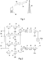
- Figure 1 illustrates a scenario where embodiments of the invention may be implemented.
- Figure 1 illustrates a scenario where a mobile station 102 has been assigned with two uplink transmission channels 104 and 106 for communication with a base station 100 or multiple base stations.
- HSUPA high-speed uplink packet access
- Other telecommunication systems and protocols may also apply dual channel transmission, e.g. GSM, GPRS, EDGE, and the embodiments of the invention are by no means limited to the UMTS system and its evolution versions including HSPA and long-term evolution (LTE).
- the dual channel transmission according to embodiments of the invention may also be applied in downlink where the base station is the transmitter.
- the dual channel transmission is referred to as dual cell transmission.
- the dual channel transmitter structure may also be applied to a scenario where the mobile station 102 communicates directly with another mobile station over a radio communication link not utilizing a fixed network infrastructure.
- the link may be a short-range radio link utilizing Bluetooth technology or a medium to long range radio link.
- the two transmission channels 104 and 106 are separated in frequency, i.e. the transmission channels 104 and 106 occupy different frequency resources.
- Figures 3A and 3B illustrate two examples of the frequency occupation of the channels allocated to the mobile station 102.
- the channels may be adjacent ( Figure 3A ) or they may be separated by one or more frequency channels not allocated to the mobile station ( Figure 3B ).
- Figures 3A and 3B let us define a center frequency Fc around which a first frequency channel and a second frequency channel are arranged symmetrically.
- an oscillator signal carrying out the up-conversion typically has a frequency which corresponds to a center frequency of the frequency channel to be used in the transmission.
- the number of transmission channels is two
- two local oscillator signals each having a frequency corresponding to one of the center frequencies of the transmission channels would be needed according to a conventional solution.
- Such an approach has, however, disadvantages. For example, one would need two frequency synthesizers, one for each frequency channel. Additionally, the two local oscillator signals can easily mix with each other in the transmitter circuitry, resulting in various mixing components.
- the transmission signals to be transmitted simultaneously in a single radio frequency signal on the first and second frequency channels Ch1 and Ch2 are first frequency-converted with a first oscillator signal having a frequency which represents a frequency offset of the frequency channels from the center frequency Fc. Then, the transmission signals are frequency-converted a second time with another oscillator signal having a frequency which corresponds to the center frequency.
- Embodiments of the invention described below show how it is arranged that the transmission signals appear on a correct frequency channel and not on a mirror frequency channel which is occupied by the other transmission signal.
- Figure 2 illustrates an example of a transmission circuitry applicable to a radio communication device according to an embodiment of the invention.
- the transmission circuitry described herein in connection with Figure 2 thus forms an embodiment of an apparatus in accordance with the present invention.
- Another embodiment of the apparatus is a radio communication device comprising the transmission circuitry and other components, e.g. a user interface and/or a memory unit storing software and data.
- the dual channel transmission is achieved by using a single transmitter chain instead of one for each frequency channel, thereby overcoming the problem of increased cost and size of the transmitter structure.
- the transmission circuitry receives a first transmission signal to be transmitted on a first frequency channel Ch1 and represented by its in-phase (I) component I1 and quadrature (Q) component Q1 and a second transmission signal to be transmitted on a second frequency channel Ch2 and represented by its I component I2 and Q component Q2.
- the first and second transmission signals may be of another type, e.g. a spread spectrum signal with a higher bandwidth, but that might obscure the description with unnecessary complexity.
- the transmission signals may be baseband signals having frequencies f1 and f2 of 1 MHz, for example.
- the I and Q components of the first and second transmission signals are arranged in the transmission circuitry into a plurality of processing branches, as illustrated in Figure 2 .
- the I component I1 is applied to a first subtractor 20 and a first adder 21
- the Q component Q1 is applied to a second subtractor 22 and a second adder 23
- the I component I2 is applied to the second subtractor 22 and the second adder 23
- the Q component Q2 is applied to the first subtractor 20 and the first adder 21.
- each processing branch at this stage comprises a signal component (either in-phase of quadrature component) from both the first and the second transmission signals.
- each I and Q component of both the first and second transmission signals is arranged into two processing branches.
- an intermediate signal on each processing branch is frequency-converted with an oscillator signal (LO2a or LO2b) having a first frequency which corresponds to the frequency offset of the frequency channels Ch1 and Ch2 from the center frequency Fc.
- the frequency offset may be defined as the (absolute) frequency difference between the center frequency of either frequency channel Ch1 or Ch2 and the center frequency Fc.
- the bandwidth of each frequency channel is 5 MHz and, thus, the frequency of the oscillator signal LO2 is 2.5 MHz.
- a first intermediate signal S1 representing the difference between I1 and Q2 and a fourth intermediate signal S4 representing a sum of I2 and Q1 are frequency-converted with a first local oscillator signal LO2b.
- a second intermediate signal S2 representing the sum of I1 and Q2 and a third intermediate signal S3 representing a difference between I2 and Q1 are frequency-converted with a second local oscillator signal LO2b.
- the first and second oscillator signals LO2a and LO2b may have the same frequency but a phase difference of 90 degrees in order to arrange a phase difference between the same signal components in the different processing branches.
- the signal S1 output from the first subtractor 20 is applied to a first mixer 24 having the second oscillator signal LO2b as another input, and the resulting signal is denoted as S5.
- Signal S2 output from the first adder 21 is applied to a second mixer 25 having the first oscillator signal LO2a as another input, and the resulting signal is denoted as S6.
- Signal S3 output from the second subtractor 22 is applied to a third mixer 26 having the first oscillator signal LO2a as another input, and the resulting signal is denoted as S7.
- Signal S4 output from the second adder 23 is applied to a fourth mixer 27 having the second oscillator signal LO2b as another input, and the resulting signal is denoted as S8.
- the frequency-converted intermediate signals S5 and S7 are summed together in a third adder 28 to form a first combined intermediate signal S9.
- the frequency-converted intermediate signals S6 and S8 are summed together in a fourth adder 29 to form a second combined intermediate signal S10.
- each combined intermediate signal S9 and S10 is converted from a digital domain into an analog domain in respective digital-to-analog converters 30 and 31.
- the resulting analog signals are then low-pass filtered in low-pass filters 32 and 33 in order to smooth the D/A-converted signals by removing high-frequency components obtained as a result of the D/A conversion.
- the D/A-converted combined intermediate signals are up-converted into the radio frequency used in the transmission.
- the first combined intermediate signal S9 is applied after the low-pass filtering to a fifth mixer 34 having a third oscillator signal LO1b as another input.
- the second combined intermediate signal S10 is applied after the low-pass filtering to a sixth mixer 35 having a fourth oscillator signal LO1a as another input.
- the frequency of the third and fourth oscillator signals LO1a and LO1b corresponds to the center frequency Fc around which the first and second frequency channels are arranged in a frequency spectrum.
- the phase difference between the third and fourth oscillator signals LO1a and LO1b is again 90 degrees.
- signals S11 and S12 are combined in a fifth adder 36 to produce an up-converted (radio frequency, RF) transmission signal RFout having the frequency-converted first transmission signal on the first frequency channel and the frequency-converted second transmission signal on the second frequency channel.
- the transmission signal may be applied to a power amplifier, a filter and an antenna for transmission to a radio interface.
- the RF transmission signal RFout includes two components wherein the first component sin[( ⁇ c - ⁇ d + ⁇ 1 )t] represents the first transmission signal (both in-phase and quadrature components) now frequency-converted from frequency f1 to frequency Fc-f d +f1 which corresponds to the first frequency channel Ch1 in Figure 3A .
- the second component cos[( ⁇ c , ⁇ d + ⁇ 2 )t] represents the second transmission signal (both in-phase and quadrature components) now frequency-converted from frequency f2 to frequency Fc+f d +f2 which corresponds to the second frequency channel Ch2 in Figure 3A .
- the RF transmission signal RFout does not include mirror frequency components for either transmission signal. This is enabled by the phase manipulation in the transmission circuitry. Let us remind that signal components of each first and second transmission signal are included in two processing branches until the final combination in the fifth adder 36. The phases of the intermediate signals in the transmission circuitry are manipulated so that the same signal components related to the mirror frequency in the processing branches have opposite phases when the signal components are applied to the fifth adder 36. As a consequence, the signal components on the mirror frequencies and having opposite phases in the different processing branches negate each other in the summing process, where the branches are combined, and the mirror frequency is effectively cancelled.
- the up-converted transmission signals appear above the center frequencies of the frequency channels.
- the actual location of the transmission signals in the frequency channels is not of particular relevance, as long as they reside within the frequency channel.
- the location and the bandwidth of the transmission signals may vary within the boundaries of the frequency channel.
- the two frequency channels Ch1 and Ch2 are adjacent frequency channels ( Figure 3A ).
- the same transmission circuitry may be used when the frequency channels are separated by one or more other frequency channels not allocated to the mobile station employing the transmission circuitry.
- the higher (or an arbitrary) frequency separation between the frequency channels may be achieved by adjusting the frequency of the oscillator signals LO2a and LO2b input to the mixers 24 to 27.
- the frequency of this oscillator signal carrying out the first frequency conversion in the processing branches defines the frequency separation of the frequency channels Ch1 and Ch2.
- the frequency separation between the frequency channels allocated to the mobile station is 15 MHz, meaning that two other frequency channels may be allocated between Ch1 and Ch2.
- the higher frequency separation actually means that the intermediate signals S5 to S10 are located on a higher frequency than in the case of adjacent frequency channels. Therefore, when the transmission circuitry is configured to implement the higher frequency separation, the D/A converters 30 and 31 may be arranged to comply with higher bandwidth requirements.
- the order of the bandwidth requirement may be about a few dozen MHz, depending on the maximum frequency separation available in the radio spectrum or supported by the transmission circuitry of the mobile station.
- the bandwidth of the low-pass filters 32 and 33 may be widened to comply with the higher maximum frequency of the intermediate signals S5 to S10. Since the maximum bandwidth of the transmission signals remains constant regardless of the frequency separation of the frequency channels, a band below the frequency band of the intermediate signals S5 to S10 exists where no signal component is present. As a consequence, the low-pass filters 32 and 33 may be replaced by band-pass filters when the frequency channels are not adjacent in order to filter out spurious signal components below the effective band of the intermediate signals S9 and S10 input to the filters.
- the transmission circuitry may include both low-pass filters 32, 33 and band-pass filters (not shown), and the selection between the utilization of the low-pass filters 32, 33 and band-pass filters may be carried out by using switches controlled by a controller configured to select appropriate filters on the basis of whether adjacent or separated frequency channels are allocated to the mobile station.
- a controller configured to select appropriate filters on the basis of whether adjacent or separated frequency channels are allocated to the mobile station.
- filtering parameters low-pass or band-pass property, bandwidth, pass-band and stop-band frequencies, etc.
- the controller may obtain information on the frequency separation implicitly from a frequency of the oscillator signals LO2a/LO2b or in an explicit signal received through an input interface of the controller.
- the same input signal may control a frequency synthesizer (not shown) to produce the signals LO2a and LO2b with desired frequency and the controller to select the transmission parameters for the filters.
- Figure 4 illustrates the operation in a general level so that the general idea of the operation of the circuitry can be appreciated
- Figure 5 illustrates the operation in greater detail.
- a first and a second transmission signal is obtained.
- the first transmission signal is to be transmitted on a first frequency channel
- the second transmission signal is to be transmitted on a second frequency channel, wherein the first frequency channel and the second frequency channel are arranged symmetrically around a center frequency Fc.
- each processing branch includes signal components of both the first transmission signal and the second transmission signal.
- each signal component is frequency-converted first with an oscillator signal having a first frequency which corresponds to a frequency offset from the center frequency and again with another oscillator signal having a second frequency which corresponds to the center frequency.
- one oscillator signal having the first frequency and one oscillator signal having the second frequency is applied to each processing branch.
- phase of the signal components in different processing branches are manipulated so that the signal components of both first transmission signal and second transmission signal appearing on a mirror frequency channel as a result of the frequency-conversion with the oscillator signal having the second frequency have opposite phases in different processing branches.
- the undesired mirror frequency components of both the first and the second transmission signals are effectively cancelled.
- the transmission circuitry described above in connection with Figure 2 is an embodiment of an apparatus comprising the means for executing the process of Figure 4 .
- blocks 400 and 402 may have the same functionality as the corresponding blocks in Figure 4 .
- block 500 sum and difference components are derived from the first and second transmission signals.
- in-phase component of each transmission signal is summed with a quadrature component of the other transmission signal to obtain two sum components (signals) I1+Q2 and I2+Q1.
- the quadrature component of each transmission signal is subtracted from the in-phase component of the other transmission signal to obtain two difference components I1-Q2 and 12-Q1.
- Each sum and difference component is assigned to a different processing branch in the transmission circuitry.
- the sum and difference correspond to the respective intermediate signals S1 to S4 in Figure 2 .
- an oscillator signal having the first frequency corresponding is applied to each processing branch.
- each of the sum and difference components is up-converted to a frequency which corresponds to the frequency offset of the first and second frequency channels from the center frequency Fc.
- the phases of the sum and difference components in different processing branches are manipulated.
- the manipulation may comprise arranging the sum component I1+Q2 and difference component I2-Q1 to have a phase which leads the phase of the sum component I2+Q1 and difference component I1-Q2 by 90 degrees (or ⁇ /2).
- the phase manipulation may be carried out by arranging the phase difference in the oscillator signals having the first frequency.
- the same oscillator signal having the first frequency is applied to every processing branch, and processing branches having the sum component I2+Q1 and difference component I1-Q2 include a delay component which delays the components I2+Q1 and I1-Q2 by ⁇ /2 to induce the phase difference.
- the sum and difference components are combined by summing sum signal components together (in adder 29) and difference signal components together (in adder 28).
- the components in the combined processing branches are frequency-converted again. Each component is now up-converted by an oscillator signal having the second frequency corresponding to the center frequency Fc.
- the phases of the components up-converted in block 508 are manipulated so that the same in-phase and quadrature components in different processing branches either have the same phase or opposite phase.
- the processing branch carrying the sum components is in this example manipulated to lead the phase of the processing branch carrying the difference components by 90 degrees (or ⁇ /2).
- the phase manipulation may be included in the phases of the oscillator signals applied to the different processing branches, or the processing branch carrying the difference components may be delayed by 90 degrees with a delay component.
- the phase manipulation may be carried out in connection with the frequency-conversion by applying the phase manipulation to the oscillator signals, or the phase manipulation may be carried out as separated from the frequency conversion.
- the processing branches carrying the sum and difference components are combined together.
- the same components having the same phase in different processing branches are summed together to form a transmission signal, and the same components having the opposite phases in different processing branches are summed together and cancelled.
- the combined transmission signal is applied to an RF filter, a power amplifier, and an antenna.
- the computer program may be stored on a computer program distribution medium readable by a computer or a processor.
- the computer program medium may be, for example but not limited to, an electric, magnetic, optical, infrared or semiconductor system, device or transmission medium.
- the computer program medium may include at least one of the following media: a computer readable medium, a program storage medium, a record medium, a computer readable memory, a random access memory, an erasable programmable read-only memory, a computer readable software distribution package, a computer readable signal, a computer readable telecommunications signal, computer readable printed matter, and a computer readable compressed software package.
- the transmission circuitry may include other functional components than these disclosed. The description of such components would obscure the embodiments of the invention with unnecessary details and, therefore, such description is omitted. It is equally obvious that a number of different practical implementations exists. For example, the processing in the digital domain described in connection with Figure 3 may be replaced by analog processing techniques.
- the communication device may transmit both uplink frequency channels with the same transmission power, or a different transmission power may be applied to first and second transmission channels.
- the transmission power may be carried out by a transmission power control circuitry (not shown) configured to apply power control settings to the first and second transmission signals by adjusting the level of the I and Q signals in the transmission circuitry.
- the transmission power control settings may be determined on the basis of transmission power control commands received from a serving base station.
- the oscillator signals having the first frequency LO2a and LO2b may be produced from a single oscillator signal having the frequency of LO1 by means of digital signal processing or by means of analog frequency dividers instead of providing two independent oscillator signals with different frequencies.
- the mixers 24 to 27 may be replaced by a single multiplier structure implemented by hardware to which each signal (sum and difference) component is alternately applied. When considering the functionality of this operation, it corresponds to the situation where there is a separate mixer for each signal.
- Other alternative solutions can obviously be derived by one skilled in the art, and the scope of the present inventions should not be seen as limited by exemplary solutions described above.
Landscapes
- Engineering & Computer Science (AREA)
- Computer Networks & Wireless Communication (AREA)
- Signal Processing (AREA)
- Transmitters (AREA)
- Transceivers (AREA)
Priority Applications (1)
| Application Number | Priority Date | Filing Date | Title |
|---|---|---|---|
| PL09846423T PL2446540T3 (pl) | 2009-06-23 | 2009-06-23 | Transmisja dwukanałowa |
Applications Claiming Priority (1)
| Application Number | Priority Date | Filing Date | Title |
|---|---|---|---|
| PCT/FI2009/050558 WO2010149822A1 (en) | 2009-06-23 | 2009-06-23 | Dual channel transmission |
Publications (3)
| Publication Number | Publication Date |
|---|---|
| EP2446540A1 EP2446540A1 (en) | 2012-05-02 |
| EP2446540A4 EP2446540A4 (en) | 2017-01-25 |
| EP2446540B1 true EP2446540B1 (en) | 2018-04-25 |
Family
ID=43386065
Family Applications (1)
| Application Number | Title | Priority Date | Filing Date |
|---|---|---|---|
| EP09846423.3A Not-in-force EP2446540B1 (en) | 2009-06-23 | 2009-06-23 | Dual channel transmission |
Country Status (6)
| Country | Link |
|---|---|
| US (1) | US8665995B2 (pl) |
| EP (1) | EP2446540B1 (pl) |
| CN (1) | CN102460978B (pl) |
| ES (1) | ES2674261T3 (pl) |
| PL (1) | PL2446540T3 (pl) |
| WO (1) | WO2010149822A1 (pl) |
Families Citing this family (6)
| Publication number | Priority date | Publication date | Assignee | Title |
|---|---|---|---|---|
| US8982972B2 (en) * | 2012-04-30 | 2015-03-17 | Intel Mobile Communications GmbH | Apparatus and method for processing an input signal |
| EP2706714A1 (en) * | 2012-09-10 | 2014-03-12 | Alcatel-Lucent | Signal processing device and method of processing at least two input signals for a transmitter of a communications device |
| US9054921B2 (en) | 2013-03-13 | 2015-06-09 | Intel Mobile Communications GmbH | Method and apparatus for generating a plurality of modulated signals |
| CN104796181B (zh) * | 2015-03-27 | 2017-10-10 | 中国人民解放军61469部队 | 短波双天线数字化通信系统及其自动接收校验方法 |
| ES2812999A1 (es) * | 2019-09-18 | 2021-03-18 | Univ Valladolid | Tablero tecnológico con material lignocelulósico |
| CN114928365A (zh) * | 2022-04-27 | 2022-08-19 | 湖南迈克森伟电子科技有限公司 | 一种用于信号处理的方法和装置 |
Family Cites Families (9)
| Publication number | Priority date | Publication date | Assignee | Title |
|---|---|---|---|---|
| US5638401A (en) * | 1995-01-31 | 1997-06-10 | Ericsson Inc. | Method and apparatus for generating plural quadrature modulated carriers |
| FI112741B (fi) | 1998-11-26 | 2003-12-31 | Nokia Corp | Menetelmä ja järjestely RF-signaalien lähettämiseksi ja vastaanottamiseksi tiedonsiirtojärjestelmien erilaisissa radiorajapinnoissa |
| FR2791506B1 (fr) * | 1999-03-23 | 2001-06-22 | France Telecom | Emetteur radiofrequence a fort degre d'integration et avec annulation d'image, eventuellement auto-calibree |
| WO2001039364A1 (en) * | 1999-11-22 | 2001-05-31 | Parthus Technologies Plc. | Two stage quatrature down converter for gps and glonass |
| US6370372B1 (en) * | 2000-09-25 | 2002-04-09 | Conexant Systems, Inc. | Subharmonic mixer circuit and method |
| US6952593B2 (en) | 2001-08-07 | 2005-10-04 | Matsushita Mobile Communications Development Corporation Of U.S.A. | Multi-band tranceivers with reduced frequency sources for digital transmissions |
| JP4708076B2 (ja) | 2005-04-14 | 2011-06-22 | 三星電子株式会社 | ダウンコンバータ及びアップコンバータ |
| JP2006311353A (ja) | 2005-04-28 | 2006-11-09 | Samsung Electronics Co Ltd | ダウンコンバータおよびアップコンバータ |
| JP2009105558A (ja) * | 2007-10-22 | 2009-05-14 | Sony Corp | 信号処理装置、信号処理装置の制御方法、デジタル放送受信装置、及び、デジタル放送受信装置の制御方法 |
-
2009
- 2009-06-23 CN CN200980160040.XA patent/CN102460978B/zh not_active Expired - Fee Related
- 2009-06-23 PL PL09846423T patent/PL2446540T3/pl unknown
- 2009-06-23 WO PCT/FI2009/050558 patent/WO2010149822A1/en not_active Ceased
- 2009-06-23 US US13/380,801 patent/US8665995B2/en not_active Expired - Fee Related
- 2009-06-23 EP EP09846423.3A patent/EP2446540B1/en not_active Not-in-force
- 2009-06-23 ES ES09846423.3T patent/ES2674261T3/es active Active
Non-Patent Citations (1)
| Title |
|---|
| None * |
Also Published As
| Publication number | Publication date |
|---|---|
| CN102460978A (zh) | 2012-05-16 |
| EP2446540A4 (en) | 2017-01-25 |
| ES2674261T3 (es) | 2018-06-28 |
| CN102460978B (zh) | 2015-08-12 |
| US20120170682A1 (en) | 2012-07-05 |
| WO2010149822A1 (en) | 2010-12-29 |
| US8665995B2 (en) | 2014-03-04 |
| EP2446540A1 (en) | 2012-05-02 |
| PL2446540T3 (pl) | 2018-09-28 |
Similar Documents
| Publication | Publication Date | Title |
|---|---|---|
| EP2446540B1 (en) | Dual channel transmission | |
| US10355769B2 (en) | Narrowband signal transport sub-system for distributed antenna system | |
| EP2396890B1 (en) | Multi-band aggregated spectrum receiver employing frequency source reuse | |
| US8204537B2 (en) | Multiple frequency band information signal frequency band conversion | |
| CN100377498C (zh) | 下变频以多调制格式发送的信号到公共中频的方法和装置 | |
| US7372927B2 (en) | Digital filter for software-defined radio system, digital intermediate frequency signal processing apparatus having the digital filter, and method thereof | |
| US20090058475A1 (en) | Apparatus and method for digital frequency up-conversion | |
| KR102568684B1 (ko) | 분산형 안테나 시스템에서 디지털 데이터를 전송하는 방법 | |
| EP3264700B1 (en) | Receiver and signal processing method | |
| CN110601704B (zh) | 减小接收底噪的方法、装置、计算机设备和可读存储介质 | |
| CN103957017B (zh) | 一种多模移动通信系统的信号中频发射装置 | |
| CN102918923B (zh) | 用于发射/接收在一个或者多个第一频带中接收/发射的电磁信号的方法和装置 | |
| US20140051365A1 (en) | Method and device for sending signals between a radio frequency circuit and a baseband circuit | |
| EP3119007B1 (en) | Multi-mixer system and associated receiver and signal processing method | |
| US6996188B2 (en) | Multiple sub-channel modulation and demodulation with arbitrarily defined channel spacing and sampling rates | |
| US20100261435A1 (en) | Multiple frequency band information signal frequency band compression | |
| US7058037B1 (en) | Radio frequency transmitting device of mobile radio communication base station system in code division multiple access system | |
| US20100261437A1 (en) | Multiple frequency band information signal universal front end | |
| KR100825508B1 (ko) | 대역 통과 표본화에 의한 복수의 무선 처리 신호들에 대한동시 하향 변환 장치 및 방법 | |
| JP2001127736A (ja) | Cdma方式移動通信基地局システムの無線周波数送信装置 | |
| JP2013168701A (ja) | 送受信モジュール | |
| US20240090052A1 (en) | Enhanced bandwidth wireless communication system | |
| CN113556145B (zh) | 一种数据处理的方法及装置、电子设备、存储介质 | |
| US20150072636A1 (en) | Dual Channel Reception | |
| KR102421021B1 (ko) | 국부 발진기 |
Legal Events
| Date | Code | Title | Description |
|---|---|---|---|
| PUAI | Public reference made under article 153(3) epc to a published international application that has entered the european phase |
Free format text: ORIGINAL CODE: 0009012 |
|
| 17P | Request for examination filed |
Effective date: 20111110 |
|
| AK | Designated contracting states |
Kind code of ref document: A1 Designated state(s): AT BE BG CH CY CZ DE DK EE ES FI FR GB GR HR HU IE IS IT LI LT LU LV MC MK MT NL NO PL PT RO SE SI SK TR |
|
| DAX | Request for extension of the european patent (deleted) | ||
| REG | Reference to a national code |
Ref country code: HK Ref legal event code: DE Ref document number: 1169522 Country of ref document: HK |
|
| RAP1 | Party data changed (applicant data changed or rights of an application transferred) |
Owner name: NOKIA CORPORATION |
|
| RAP1 | Party data changed (applicant data changed or rights of an application transferred) |
Owner name: NOKIA TECHNOLOGIES OY |
|
| RA4 | Supplementary search report drawn up and despatched (corrected) |
Effective date: 20161223 |
|
| RIC1 | Information provided on ipc code assigned before grant |
Ipc: H03D 7/18 20060101ALI20161219BHEP Ipc: H03D 7/16 20060101ALI20161219BHEP Ipc: H04B 1/405 20150101ALI20161219BHEP Ipc: H04B 1/00 20060101AFI20161219BHEP |
|
| GRAP | Despatch of communication of intention to grant a patent |
Free format text: ORIGINAL CODE: EPIDOSNIGR1 |
|
| RIC1 | Information provided on ipc code assigned before grant |
Ipc: H04B 1/00 20060101AFI20171020BHEP Ipc: H03D 7/16 20060101ALI20171020BHEP Ipc: H03D 7/18 20060101ALI20171020BHEP Ipc: H04B 1/405 20150101ALI20171020BHEP |
|
| INTG | Intention to grant announced |
Effective date: 20171107 |
|
| GRAA | (expected) grant |
Free format text: ORIGINAL CODE: 0009210 |
|
| GRAS | Grant fee paid |
Free format text: ORIGINAL CODE: EPIDOSNIGR3 |
|
| AK | Designated contracting states |
Kind code of ref document: B1 Designated state(s): AT BE BG CH CY CZ DE DK EE ES FI FR GB GR HR HU IE IS IT LI LT LU LV MC MK MT NL NO PL PT RO SE SI SK TR |
|
| REG | Reference to a national code |
Ref country code: GB Ref legal event code: FG4D |
|
| REG | Reference to a national code |
Ref country code: CH Ref legal event code: EP |
|
| REG | Reference to a national code |
Ref country code: AT Ref legal event code: REF Ref document number: 993914 Country of ref document: AT Kind code of ref document: T Effective date: 20180515 |
|
| REG | Reference to a national code |
Ref country code: IE Ref legal event code: FG4D |
|
| REG | Reference to a national code |
Ref country code: DE Ref legal event code: R096 Ref document number: 602009052032 Country of ref document: DE |
|
| REG | Reference to a national code |
Ref country code: FR Ref legal event code: PLFP Year of fee payment: 10 |
|
| REG | Reference to a national code |
Ref country code: ES Ref legal event code: FG2A Ref document number: 2674261 Country of ref document: ES Kind code of ref document: T3 Effective date: 20180628 |
|
| REG | Reference to a national code |
Ref country code: SE Ref legal event code: TRGR |
|
| REG | Reference to a national code |
Ref country code: NL Ref legal event code: FP |
|
| REG | Reference to a national code |
Ref country code: LT Ref legal event code: MG4D |
|
| PG25 | Lapsed in a contracting state [announced via postgrant information from national office to epo] |
Ref country code: BG Free format text: LAPSE BECAUSE OF FAILURE TO SUBMIT A TRANSLATION OF THE DESCRIPTION OR TO PAY THE FEE WITHIN THE PRESCRIBED TIME-LIMIT Effective date: 20180725 Ref country code: LT Free format text: LAPSE BECAUSE OF FAILURE TO SUBMIT A TRANSLATION OF THE DESCRIPTION OR TO PAY THE FEE WITHIN THE PRESCRIBED TIME-LIMIT Effective date: 20180425 Ref country code: NO Free format text: LAPSE BECAUSE OF FAILURE TO SUBMIT A TRANSLATION OF THE DESCRIPTION OR TO PAY THE FEE WITHIN THE PRESCRIBED TIME-LIMIT Effective date: 20180725 |
|
| PG25 | Lapsed in a contracting state [announced via postgrant information from national office to epo] |
Ref country code: GR Free format text: LAPSE BECAUSE OF FAILURE TO SUBMIT A TRANSLATION OF THE DESCRIPTION OR TO PAY THE FEE WITHIN THE PRESCRIBED TIME-LIMIT Effective date: 20180726 Ref country code: HR Free format text: LAPSE BECAUSE OF FAILURE TO SUBMIT A TRANSLATION OF THE DESCRIPTION OR TO PAY THE FEE WITHIN THE PRESCRIBED TIME-LIMIT Effective date: 20180425 Ref country code: LV Free format text: LAPSE BECAUSE OF FAILURE TO SUBMIT A TRANSLATION OF THE DESCRIPTION OR TO PAY THE FEE WITHIN THE PRESCRIBED TIME-LIMIT Effective date: 20180425 |
|
| REG | Reference to a national code |
Ref country code: AT Ref legal event code: MK05 Ref document number: 993914 Country of ref document: AT Kind code of ref document: T Effective date: 20180425 |
|
| PG25 | Lapsed in a contracting state [announced via postgrant information from national office to epo] |
Ref country code: PT Free format text: LAPSE BECAUSE OF FAILURE TO SUBMIT A TRANSLATION OF THE DESCRIPTION OR TO PAY THE FEE WITHIN THE PRESCRIBED TIME-LIMIT Effective date: 20180827 |
|
| REG | Reference to a national code |
Ref country code: HK Ref legal event code: WD Ref document number: 1169522 Country of ref document: HK |
|
| REG | Reference to a national code |
Ref country code: DE Ref legal event code: R097 Ref document number: 602009052032 Country of ref document: DE |
|
| PG25 | Lapsed in a contracting state [announced via postgrant information from national office to epo] |
Ref country code: RO Free format text: LAPSE BECAUSE OF FAILURE TO SUBMIT A TRANSLATION OF THE DESCRIPTION OR TO PAY THE FEE WITHIN THE PRESCRIBED TIME-LIMIT Effective date: 20180425 Ref country code: CZ Free format text: LAPSE BECAUSE OF FAILURE TO SUBMIT A TRANSLATION OF THE DESCRIPTION OR TO PAY THE FEE WITHIN THE PRESCRIBED TIME-LIMIT Effective date: 20180425 Ref country code: SK Free format text: LAPSE BECAUSE OF FAILURE TO SUBMIT A TRANSLATION OF THE DESCRIPTION OR TO PAY THE FEE WITHIN THE PRESCRIBED TIME-LIMIT Effective date: 20180425 Ref country code: AT Free format text: LAPSE BECAUSE OF FAILURE TO SUBMIT A TRANSLATION OF THE DESCRIPTION OR TO PAY THE FEE WITHIN THE PRESCRIBED TIME-LIMIT Effective date: 20180425 Ref country code: EE Free format text: LAPSE BECAUSE OF FAILURE TO SUBMIT A TRANSLATION OF THE DESCRIPTION OR TO PAY THE FEE WITHIN THE PRESCRIBED TIME-LIMIT Effective date: 20180425 Ref country code: DK Free format text: LAPSE BECAUSE OF FAILURE TO SUBMIT A TRANSLATION OF THE DESCRIPTION OR TO PAY THE FEE WITHIN THE PRESCRIBED TIME-LIMIT Effective date: 20180425 |
|
| REG | Reference to a national code |
Ref country code: CH Ref legal event code: PL |
|
| PLBE | No opposition filed within time limit |
Free format text: ORIGINAL CODE: 0009261 |
|
| STAA | Information on the status of an ep patent application or granted ep patent |
Free format text: STATUS: NO OPPOSITION FILED WITHIN TIME LIMIT |
|
| REG | Reference to a national code |
Ref country code: BE Ref legal event code: MM Effective date: 20180630 |
|
| REG | Reference to a national code |
Ref country code: IE Ref legal event code: MM4A |
|
| PG25 | Lapsed in a contracting state [announced via postgrant information from national office to epo] |
Ref country code: LU Free format text: LAPSE BECAUSE OF NON-PAYMENT OF DUE FEES Effective date: 20180623 Ref country code: MC Free format text: LAPSE BECAUSE OF FAILURE TO SUBMIT A TRANSLATION OF THE DESCRIPTION OR TO PAY THE FEE WITHIN THE PRESCRIBED TIME-LIMIT Effective date: 20180425 |
|
| 26N | No opposition filed |
Effective date: 20190128 |
|
| PG25 | Lapsed in a contracting state [announced via postgrant information from national office to epo] |
Ref country code: CH Free format text: LAPSE BECAUSE OF NON-PAYMENT OF DUE FEES Effective date: 20180630 Ref country code: IE Free format text: LAPSE BECAUSE OF NON-PAYMENT OF DUE FEES Effective date: 20180623 Ref country code: LI Free format text: LAPSE BECAUSE OF NON-PAYMENT OF DUE FEES Effective date: 20180630 |
|
| PG25 | Lapsed in a contracting state [announced via postgrant information from national office to epo] |
Ref country code: BE Free format text: LAPSE BECAUSE OF NON-PAYMENT OF DUE FEES Effective date: 20180630 Ref country code: SI Free format text: LAPSE BECAUSE OF FAILURE TO SUBMIT A TRANSLATION OF THE DESCRIPTION OR TO PAY THE FEE WITHIN THE PRESCRIBED TIME-LIMIT Effective date: 20180425 |
|
| PGFP | Annual fee paid to national office [announced via postgrant information from national office to epo] |
Ref country code: IT Payment date: 20190620 Year of fee payment: 11 Ref country code: PL Payment date: 20190515 Year of fee payment: 11 Ref country code: DE Payment date: 20190612 Year of fee payment: 11 Ref country code: NL Payment date: 20190612 Year of fee payment: 11 Ref country code: FI Payment date: 20190610 Year of fee payment: 11 |
|
| PGFP | Annual fee paid to national office [announced via postgrant information from national office to epo] |
Ref country code: SE Payment date: 20190611 Year of fee payment: 11 Ref country code: FR Payment date: 20190510 Year of fee payment: 11 |
|
| PGFP | Annual fee paid to national office [announced via postgrant information from national office to epo] |
Ref country code: GB Payment date: 20190619 Year of fee payment: 11 Ref country code: ES Payment date: 20190701 Year of fee payment: 11 |
|
| PG25 | Lapsed in a contracting state [announced via postgrant information from national office to epo] |
Ref country code: MT Free format text: LAPSE BECAUSE OF NON-PAYMENT OF DUE FEES Effective date: 20180623 |
|
| PG25 | Lapsed in a contracting state [announced via postgrant information from national office to epo] |
Ref country code: TR Free format text: LAPSE BECAUSE OF FAILURE TO SUBMIT A TRANSLATION OF THE DESCRIPTION OR TO PAY THE FEE WITHIN THE PRESCRIBED TIME-LIMIT Effective date: 20180425 |
|
| PG25 | Lapsed in a contracting state [announced via postgrant information from national office to epo] |
Ref country code: HU Free format text: LAPSE BECAUSE OF FAILURE TO SUBMIT A TRANSLATION OF THE DESCRIPTION OR TO PAY THE FEE WITHIN THE PRESCRIBED TIME-LIMIT; INVALID AB INITIO Effective date: 20090623 |
|
| PG25 | Lapsed in a contracting state [announced via postgrant information from national office to epo] |
Ref country code: MK Free format text: LAPSE BECAUSE OF NON-PAYMENT OF DUE FEES Effective date: 20180425 Ref country code: CY Free format text: LAPSE BECAUSE OF FAILURE TO SUBMIT A TRANSLATION OF THE DESCRIPTION OR TO PAY THE FEE WITHIN THE PRESCRIBED TIME-LIMIT Effective date: 20180425 |
|
| PG25 | Lapsed in a contracting state [announced via postgrant information from national office to epo] |
Ref country code: IS Free format text: LAPSE BECAUSE OF FAILURE TO SUBMIT A TRANSLATION OF THE DESCRIPTION OR TO PAY THE FEE WITHIN THE PRESCRIBED TIME-LIMIT Effective date: 20180825 |
|
| REG | Reference to a national code |
Ref country code: DE Ref legal event code: R119 Ref document number: 602009052032 Country of ref document: DE |
|
| REG | Reference to a national code |
Ref country code: FI Ref legal event code: MAE |
|
| PG25 | Lapsed in a contracting state [announced via postgrant information from national office to epo] |
Ref country code: FI Free format text: LAPSE BECAUSE OF NON-PAYMENT OF DUE FEES Effective date: 20200623 |
|
| REG | Reference to a national code |
Ref country code: NL Ref legal event code: MM Effective date: 20200701 |
|
| GBPC | Gb: european patent ceased through non-payment of renewal fee |
Effective date: 20200623 |
|
| PG25 | Lapsed in a contracting state [announced via postgrant information from national office to epo] |
Ref country code: GB Free format text: LAPSE BECAUSE OF NON-PAYMENT OF DUE FEES Effective date: 20200623 Ref country code: FR Free format text: LAPSE BECAUSE OF NON-PAYMENT OF DUE FEES Effective date: 20200630 Ref country code: NL Free format text: LAPSE BECAUSE OF NON-PAYMENT OF DUE FEES Effective date: 20200701 |
|
| PG25 | Lapsed in a contracting state [announced via postgrant information from national office to epo] |
Ref country code: DE Free format text: LAPSE BECAUSE OF NON-PAYMENT OF DUE FEES Effective date: 20210101 Ref country code: SE Free format text: LAPSE BECAUSE OF NON-PAYMENT OF DUE FEES Effective date: 20200624 |
|
| REG | Reference to a national code |
Ref country code: SE Ref legal event code: EUG |
|
| PG25 | Lapsed in a contracting state [announced via postgrant information from national office to epo] |
Ref country code: IT Free format text: LAPSE BECAUSE OF NON-PAYMENT OF DUE FEES Effective date: 20200623 |
|
| REG | Reference to a national code |
Ref country code: ES Ref legal event code: FD2A Effective date: 20211129 |
|
| PG25 | Lapsed in a contracting state [announced via postgrant information from national office to epo] |
Ref country code: ES Free format text: LAPSE BECAUSE OF NON-PAYMENT OF DUE FEES Effective date: 20200624 |
|
| PG25 | Lapsed in a contracting state [announced via postgrant information from national office to epo] |
Ref country code: PL Free format text: LAPSE BECAUSE OF NON-PAYMENT OF DUE FEES Effective date: 20200623 |