EP2445004A1 - Laminated wiring board - Google Patents
Laminated wiring board Download PDFInfo
- Publication number
- EP2445004A1 EP2445004A1 EP10789375A EP10789375A EP2445004A1 EP 2445004 A1 EP2445004 A1 EP 2445004A1 EP 10789375 A EP10789375 A EP 10789375A EP 10789375 A EP10789375 A EP 10789375A EP 2445004 A1 EP2445004 A1 EP 2445004A1
- Authority
- EP
- European Patent Office
- Prior art keywords
- silicon substrate
- resistance silicon
- high resistance
- face
- recess
- Prior art date
- Legal status (The legal status is an assumption and is not a legal conclusion. Google has not performed a legal analysis and makes no representation as to the accuracy of the status listed.)
- Granted
Links
Images






Classifications
-
- H—ELECTRICITY
- H10—SEMICONDUCTOR DEVICES; ELECTRIC SOLID-STATE DEVICES NOT OTHERWISE PROVIDED FOR
- H10W—GENERIC PACKAGES, INTERCONNECTIONS, CONNECTORS OR OTHER CONSTRUCTIONAL DETAILS OF DEVICES COVERED BY CLASS H10
- H10W70/00—Package substrates; Interposers; Redistribution layers [RDL]
- H10W70/60—Insulating or insulated package substrates; Interposers; Redistribution layers
- H10W70/67—Insulating or insulated package substrates; Interposers; Redistribution layers characterised by their insulating layers or insulating parts
- H10W70/69—Insulating materials thereof
- H10W70/698—Semiconductor materials that are electrically insulating, e.g. undoped silicon
-
- H—ELECTRICITY
- H10—SEMICONDUCTOR DEVICES; ELECTRIC SOLID-STATE DEVICES NOT OTHERWISE PROVIDED FOR
- H10W—GENERIC PACKAGES, INTERCONNECTIONS, CONNECTORS OR OTHER CONSTRUCTIONAL DETAILS OF DEVICES COVERED BY CLASS H10
- H10W70/00—Package substrates; Interposers; Redistribution layers [RDL]
- H10W70/60—Insulating or insulated package substrates; Interposers; Redistribution layers
- H10W70/62—Insulating or insulated package substrates; Interposers; Redistribution layers characterised by their interconnections
- H10W70/63—Vias, e.g. via plugs
- H10W70/635—Through-vias
-
- H—ELECTRICITY
- H10—SEMICONDUCTOR DEVICES; ELECTRIC SOLID-STATE DEVICES NOT OTHERWISE PROVIDED FOR
- H10W—GENERIC PACKAGES, INTERCONNECTIONS, CONNECTORS OR OTHER CONSTRUCTIONAL DETAILS OF DEVICES COVERED BY CLASS H10
- H10W70/00—Package substrates; Interposers; Redistribution layers [RDL]
- H10W70/60—Insulating or insulated package substrates; Interposers; Redistribution layers
- H10W70/62—Insulating or insulated package substrates; Interposers; Redistribution layers characterised by their interconnections
- H10W70/66—Conductive materials thereof
- H10W70/662—Semiconductor materials
-
- H—ELECTRICITY
- H10—SEMICONDUCTOR DEVICES; ELECTRIC SOLID-STATE DEVICES NOT OTHERWISE PROVIDED FOR
- H10W—GENERIC PACKAGES, INTERCONNECTIONS, CONNECTORS OR OTHER CONSTRUCTIONAL DETAILS OF DEVICES COVERED BY CLASS H10
- H10W70/00—Package substrates; Interposers; Redistribution layers [RDL]
- H10W70/60—Insulating or insulated package substrates; Interposers; Redistribution layers
- H10W70/67—Insulating or insulated package substrates; Interposers; Redistribution layers characterised by their insulating layers or insulating parts
- H10W70/68—Shapes or dispositions thereof
- H10W70/685—Shapes or dispositions thereof comprising multiple insulating layers
-
- H—ELECTRICITY
- H10—SEMICONDUCTOR DEVICES; ELECTRIC SOLID-STATE DEVICES NOT OTHERWISE PROVIDED FOR
- H10F—INORGANIC SEMICONDUCTOR DEVICES SENSITIVE TO INFRARED RADIATION, LIGHT, ELECTROMAGNETIC RADIATION OF SHORTER WAVELENGTH OR CORPUSCULAR RADIATION
- H10F39/00—Integrated devices, or assemblies of multiple devices, comprising at least one element covered by group H10F30/00, e.g. radiation detectors comprising photodiode arrays
- H10F39/80—Constructional details of image sensors
- H10F39/811—Interconnections
-
- H—ELECTRICITY
- H10—SEMICONDUCTOR DEVICES; ELECTRIC SOLID-STATE DEVICES NOT OTHERWISE PROVIDED FOR
- H10W—GENERIC PACKAGES, INTERCONNECTIONS, CONNECTORS OR OTHER CONSTRUCTIONAL DETAILS OF DEVICES COVERED BY CLASS H10
- H10W70/00—Package substrates; Interposers; Redistribution layers [RDL]
- H10W70/60—Insulating or insulated package substrates; Interposers; Redistribution layers
- H10W70/67—Insulating or insulated package substrates; Interposers; Redistribution layers characterised by their insulating layers or insulating parts
- H10W70/68—Shapes or dispositions thereof
-
- H—ELECTRICITY
- H10—SEMICONDUCTOR DEVICES; ELECTRIC SOLID-STATE DEVICES NOT OTHERWISE PROVIDED FOR
- H10W—GENERIC PACKAGES, INTERCONNECTIONS, CONNECTORS OR OTHER CONSTRUCTIONAL DETAILS OF DEVICES COVERED BY CLASS H10
- H10W90/00—Package configurations
- H10W90/701—Package configurations characterised by the relative positions of pads or connectors relative to package parts
- H10W90/721—Package configurations characterised by the relative positions of pads or connectors relative to package parts of bump connectors
- H10W90/724—Package configurations characterised by the relative positions of pads or connectors relative to package parts of bump connectors between a chip and a stacked insulating package substrate, interposer or RDL
Definitions
- the present invention relates to a multilayer wiring board such as an interposer board.
- Patent Literature 1 discloses a multilayer wiring board formed by stacking a plurality of ceramic substrates. While the ceramic substrates have various advantages, for example, in that their coefficient of linear expansion is smaller than that of resin-based substrates and that they can be flattened by polishing and the like, and techniques for providing them with through-hole electrodes have already been established, they are hard to form narrow-pitch wiring patterns and thus are not suitable for smaller sizes.
- Patent Literatures 2 and 3 disclose silicon substrates in which a portion surrounded by a ring-shaped groove (trench) having a depth equal to their thickness serves as an electric passage part.
- the multilayer wiring board in accordance with the present invention comprises a low resistance silicon substrate including an electric passage part surrounded by a ring-shaped groove having a depth equal to a thickness thereof; a first insulating layer laid on a main face on first side of the low resistance silicon substrate and formed with a first opening penetrating therethrough in the thickness direction so as to correspond to the electric passage part; and a high resistance silicon substrate laid on a main face on the first side of the first insulating layer and formed with a first recess having a depth equal to a thickness thereof so as to correspond to the first opening; wherein the low resistance silicon substrate has a predetermined resistivity, and the first high resistance silicon substrate has a resistivity higher than the predetermined resistivity; and wherein a first wiring film is disposed on a main face on the first side of the first high resistance silicon substrate and an inner face of the first recess while interposing a first insulating film, and the first wiring film is electrically connected to the electric passage
- the low resistance silicon substrate having a predetermined resistivity and the first high resistance silicon substrate having a resistivity higher than the predetermined resistivity are laid on the first side and the second side of the first insulating layer, respectively.
- the low resistance silicon substrate is provided with an electric passage part surrounded by a ring-shaped groove, while the first wiring film electrically connected to the electric passage part through the first opening of the first insulating layer is disposed on the main face on the first side of the first high resistance silicon substrate and the inner face of the first recess while interposing the first insulating film. Since the first high resistance silicon substrate is thus provided with the first wiring film, elements which differ from each other in terms of the number and positions of electrode pads can be electrically connected to each other on the first side and the second side of the multilayer wiring board.
- the first recess is formed such that an end part on second side of the first recess is included in an end face on the first side of the electric passage part when seen in the thickness direction of the first high resistance silicon substrate.
- This structure allows peripheral portions of the end part on the second side of the first recess to support the electric passage part, thereby improving mechanical strength.
- the first recess is formed such as to become broader from a main face on second side of the first high resistance silicon substrate to the main face on the first side thereof.
- This structure makes it easier to form the first wiring film on the inner face of the first recess, so as to prevent disconnections and the like from occurring within the first recess, whereby the electric connection between the electric passage part and the first wiring film can be ensured.
- the first recess prefferably be formed such that an end part on the first side of the first recess is included in an end face on the first side of the electric passage part when seen in the thickness direction of the first high resistance silicon substrate.
- the whole inner face of the first recess broadening from the second side to the first side is included in the end face on the first side of the electric passage part. This allows peripheral portions of the whole first recess to support the electric passage part, thereby improving mechanical strength.
- a void is formed within the ring-shaped groove. This structure can attain electric insulation between the electric passage part and its peripheral portions while inhibiting electric capacity from increasing.
- An electrode film may be disposed on an end face on second side of the electric passage part. This allows elements having functions different from each other to be mounted on the main face on the first side of the first high resistance silicon substrate and the main face on the second side of the low resistance silicon substrate, whereby the device as a whole can be made thinner.
- the multilayer wiring board may further comprise a second insulating layer laid on a main face on second side of the low resistance silicon substrate and formed with a second opening penetrating therethrough in the thickness direction so as to correspond to the electric passage part; and a second high resistance silicon substrate laid on a main face on the second side of the second insulating layer and formed with a second recess having a depth equal to a thickness thereof so as to correspond to the second opening; wherein the second high resistance silicon substrate has a resistivity higher than the predetermined resistivity; and wherein a second wiring film is disposed on a main face on the second side of the second high resistance silicon substrate and an inner face of the second recess while interposing the second insulating film, and the second wiring film is electrically connected to the electric passage part through the second opening.
- the present invention can electrically connect elements which are different from each other in terms of the number and positions of electrode pads to each other by using a silicon substrate.
- Fig. 1 is a plan view of the first embodiment of a device equipped with the multilayer wiring board in accordance with the present invention.
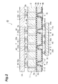
- Fig. 2 is a sectional view of the device taken along the line II-II of Fig. 1
- Fig. 3 is a bottom plan view of the device of Fig. 1 .
- an optical semiconductor element 20 and an electronic circuit element 30, each shaped like a rectangular sheet are respectively mounted on the front face side (second side) and rear face side (first side) of a rectangular-sheet-shaped multilayer wiring board 1 which is an interposer board.
- the optical semiconductor element 20 is a multichannel optical element (an array light-receiving element of 4 ⁇ 4 channels here), while the electronic circuit element 30 is a processing IC such as an amplifier array.
- the size of the electronic circuit element 30 becomes smaller than that of the optical semiconductor element 20. Since making the electronic circuit element 30, whose manufacturing process is complicated, larger than necessary is less meritorious in terms of cost, the optical semiconductor element 20 and the electronic circuit element 30 are hybrid-connected to each other through the multilayer wiring board 1 adapted to change pitches.
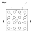
- Fig. 4 is a plan view of the multilayer wiring board of Fig. 1 .
- Fig. 5 is a sectional view of the multilayer wiring board taken along the line V-V of Fig. 4
- Fig. 6 is a bottom plan view of the multilayer wiring board of Fig. 4 .
- the multilayer wiring board 1 comprises a low resistance silicon substrate 2, an insulating layer (first insulating layer) 3 laid on the rear face (main face on the first side) 2b of the low resistance silicon substrate 2, and a high resistance silicon substrate (first high resistance silicon substrate) 4 laid on the rear face (main face on the first side) 3b of the insulating layer 3.
- the multilayer wiring board 1 is an SOI (Silicon On Insulator) substrate in which the low resistance silicon substrate 2 and the high resistance silicon substrate 4 are connected to each other through the insulating layer 3.
- SOI Silicon On Insulator
- the low resistance silicon substrate 2 has a predetermined resistivity (e.g., 0.01 ⁇ cm), while the high resistance silicon substrate 4 has a resistivity (e.g., 3 k ⁇ cm) higher than the predetermined resistivity.
- the insulating layer 3 is an oxide film made of silicon oxide or the like.
- the low resistance silicon substrate 2 includes cylindrical electric passage parts 6 each surrounded by a circular ring-shaped groove 5 having a depth equal to its thickness.
- the ring-shaped groove 5 has a depth extending from the front face 2a to rear face 2b of the low resistance silicon substrate 2 such that its bottom face becomes the front face 3a of the insulating layer 3.
- the electric passage parts 6 are disposed not only in the arrangement of 4 ⁇ 4 but also at the center thereof so as to correspond to (i.e., oppose in the thickness direction) anode pads 20a and a common cathode pad 20b in the optical semiconductor element 20 (see Figs. 1 and 2 ).
- Each electric passage part 6 is defined by the ring-shaped groove 5 formed by silicon deep etching, while electric insulation is attained by the air within the ring-shaped groove 5 (or other electrically insulating materials filling the same).
- An electrode film 7 made of a metal such as Cr/Pt/Au is disposed on the end face 6a on the front face side of each electric passage part 6.
- the electrode film 7 is formed on the end face 6a of the electric passage part 6 by resistive heating, vapor deposition by an electron beam, sputtering, plating, or the like, so as to be brought into ohmic contact with the electric passage part 6.
- Each electrode film 7 is connected to its corresponding anode pad 20a or common cathode pad 20b of the optical semiconductor element 20 through a solder bump 40 (see Figs. 1 and 2 ).
- the insulating layer 3 is formed with openings (first openings) 8 penetrating therethrough in the thickness direction thereof so as to correspond to (i.e., oppose in the thickness direction) the respective electric passage parts 6 of the low resistance silicon substrate 2.
- Each opening 8 is formed such as to be included in the end face 6b on the rear face side of its corresponding electric passage part 6 when seen in the thickness direction of the insulating layer 3.
- a conductive film 9 made of a metal such as Cr/Pt/Au is formed within each opening 8, so as to be brought into ohmic contact with the electric passage part 6.
- the high resistance silicon substrate 4 is formed with recesses (first recesses) 11 having a depth equal to the thickness thereof so as to correspond to (i.e., oppose in the thickness direction) the respective openings 8 of the insulating layer 3.
- Each recess 11 has a depth extending from the rear face 4b to front face 4a of the high resistance silicon substrate 4 such that its bottom face becomes the rear face 3b of the insulating layer 3.
- Each recess 11 is formed by wet etching or the like so as to become broader from the front face 4a to rear face 4b of the high resistance silicon substrate 4 (i.e., taper down from the rear face 4b to front face 4a of the high resistance silicon substrate 4). More specifically, when seen in the thickness direction of the high resistance silicon substrate 4, each recess 11 is formed into a truncated pyramid such that the end part (opening) on the rear face side of the recess 11 is included in the end face 6b of its corresponding electric passage part 6. Consequently, when seen in the thickness direction of the high resistance silicon substrate 4, the end part (bottom part) on the front face side of the recess 11 is also included in the end face 6b of the electric passage part 6 as a matter of course.
- the opening 8 of the insulating layer 3 is included not only in the end face 6b of its corresponding electric passage part 6, but also in the end part (bottom part) on the front face side of its corresponding recess 11.
- a wiring film (first wiring film) 13 made of a metal such as Cr/Pt/Au is disposed on the rear face 4b and the inner faces 11 a of the recesses 11 while interposing an insulating film (first insulating film) 12 which is an oxide or nitride film made of silicon oxide, silicon nitride, or the like.
- the insulating film 12 is removed from the end parts (bottom parts) on the front face side of the recesses 11, whereby the wiring film 13 is connected to the conductive film 9 at thus removed parts.
- the wiring film 13 is electrically connected to the electric passage parts 6 of the low resistance silicon substrate 2 through the openings 8 of the insulating layer 3.
- the wiring film 13 patterned on the rear face 4b of the high resistance silicon substrate 4 has pad parts 13a disposed so as to correspond to (i.e., oppose in the thickness direction) terminal electrode pads 30a of the electronic circuit element 30 (see Figs. 2 and 3 ), external interface parts 13b for electrically connecting with externals in order to feed electric power and input and output signals, and wiring parts 13c for mutually connecting the pad parts 13a, the external interface parts 13b, and portions of the wiring film 13 within the recesses 11.
- the terminal electrode pads 30a of the electronic circuit element 30 are connected to the respective pad parts 13a through their corresponding solder bumps 40 (see Figs. 2 and 3 ). Since the high resistance silicon substrate 4 itself has a high resistivity, high impedance is also maintained in terms of alternating current among the leads of the wiring film 13.
- silicon wafers made by the CZ (Czochralski) process are hard to attain higher resistance (lower impurity content)
- the high resistance silicon substrate 4 is preferably made thinner, since this allows the electrodes to attain narrower pitches and higher electric resistance values therebetween.
- the thickness of the high resistance silicon substrate 4 is preferably on the order of several 10 to 100 ⁇ m, since it becomes weaker when too thin, and may be 200 or 300 ⁇ m when not used for high frequencies.
- the thickness of the low resistance silicon substrate 2 is determined relative to the required electric resistance value.
- the electric passage part 6 having a diameter of 100 ⁇ m is formed in the low resistance silicon substrate 2 having a resistivity of 0.01 ⁇ cm, it yields 127 ⁇ /cm.
- the electric passage part 6 attains electric resistance values of about 6 ⁇ and about 1.3 ⁇ when the low resistance silicon substrate 2 has thicknesses of 500 ⁇ m and 100 ⁇ m, respectively.
- the size of the electric passage part 6 may be made greater, such as to have a diameter of 200 ⁇ m, for example.
- the thickness of the low resistance silicon substrate 2 is 100 ⁇ m here, the electric resistance value of the electric passage part 6 becomes 0.3 ⁇ .
- the low resistance silicon substrate 2 having a predetermined resistivity and the high resistance silicon substrate 4 having a resistivity higher than the predetermined resistivity are respectively laid on the front face 3a and rear face 3b of the insulating layer 3 interposed therebetween.
- the low resistance silicon substrate 2 is provided with the electric passage parts 6 surrounded by the respective ring-shaped grooves 5, while the wiring film 13 electrically connected to the electric passage parts 6 through the openings 8 of the insulating layer 3 is disposed on the rear face 4b of the high resistance silicon substrate 4 and the inner faces 11a of the recesses 11. Since the high resistance silicon substrate 4 is thus provided with the wiring film 13, the optical semiconductor element 20 and electronic circuit element 30 different from each other in terms of the number and positions of electrode pads can be electrically connected to each other on the front face side and rear face side of the multilayer wiring board 1.
- Combining the low resistance silicon substrate 2 and high resistance silicon substrate 4 together can secure mechanical strength and facilitate handling, even when the high resistance silicon substrate 4 is made thinner. This makes it unnecessary to provide wiring films on both front and rear face sides through insulating films, whereby the structure can be made simpler.
- the recesses 11 of the high resistance silicon substrate 4 are formed such as to become broader from the front face 4a to rear face 4b of the high resistance silicon substrate 4. This makes it easier to form the wiring film 13 on the inner faces 11 a of the recesses 11, so as to prevent disconnections and the like from occurring within the recesses 11, whereby the electric connection between the electric passage parts 6 of the low resistance silicon substrate 2 and the wiring film 13 can be ensured.
- Each recess 11 is formed such that the end part (opening) on the rear face side of the recess 11 is included in the end face 6b of its corresponding electric passage part 6 when seen in the thickness direction of the high resistance silicon substrate 4. Since the recess 11 is formed such as to become broader from the front face 4a to rear face 4b of the high resistance silicon substrate 4, the end part (bottom part) on the front face side of the recess 11 is also included in the end face 6b of the electric passage part 6 when seen in the thickness direction of the high resistance silicon substrate 4. This allows peripheral portions of the whole recess 11 to support the electric passage part 6, thereby improving mechanical strength.
- a void is formed within the ring-shaped groove 5 surrounding the electric passage part 6. This can attain electric insulation between the electric passage part 6 and its peripheral portions while inhibiting electric capacity from increasing.
- the mechanical strength is reinforced by the mounting of the semiconductor element 20 and thus becomes no problem in particular.
- the electrode film 7 is disposed on the end face 6a on the front face side of the electric passage part 6 of the low resistance silicon substrate 2. This allows the optical semiconductor element 20 and electronic circuit element 30 having functions different from each other to be mounted on the front face 2a of the low resistance silicon substrate 2 and the rear face 4b of the high resistance silicon substrate 4, respectively, whereby the device D as a whole can be made thinner.
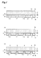
- a method of manufacturing the multilayer wiring board 1 will now be explained with reference to Figs. 7 and 8 .
- the following manufacturing steps are performed for each silicon wafer as a unit, while each multilayer wiring board 1 is obtained by dicing the silicon wafer.
- an SOI substrate in which the low resistance silicon substrate 2 and the high resistance silicon substrate 4 are connected to each other through the insulating layer 3 is prepared.
- the front and rear faces 2a, 2b of the low resistance silicon substrate 2 are implanted with ions for ohmic connection.
- silicon nitride films 41 are formed on the front face 2a of the low resistance silicon substrate 2 and the rear face 2b of the high resistance silicon substrate 4, and the recesses 11 are formed while using the silicon nitride firm 41 as a mask.
- an alkali solution such as KOH or TMAH
- the insulating layer 3 acts as a stop layer.
- the silicon nitride films 41 are removed, and the insulating film 12 is formed on the rear face 4b of the high resistance silicon substrate 4 and the inner faces 11 a of the recesses 11 by thermal oxidation or CVD.
- the oxide film formed on the front face 2a of the low resistance silicon substrate 2 when making the insulating film 12 by thermal oxidization is unnecessary and thus is removed by dry etching.
- a resist mask 42 is formed on the rear face 4b of the high resistance silicon substrate 4 and the inner faces 11 a of the recesses 11 by a spray coater, and the openings 8 are formed in the insulating layer 3 by dry etching.
- the front face 2a of the low resistance silicon substrate 2 is implanted with ions at this stage, and so is the rear face 2b of the low resistance silicon substrate 2 through the openings 8.
- the resist mask 42 is removed, and a metal film is formed by vapor deposition on the front face 2a of the low resistance silicon substrate 2, within the openings 8 of the insulating layer 3, and on the insulating film 12.
- the electrode film 7 is formed on the front face 2a of the low resistance silicon substrate 2, while the wiring film 13 is formed on the rear face 4b of the high resistance silicon substrate 4 and the inner faces 11a of the recesses 11 while interposing the insulating film 12. Annealing is performed at this stage if necessary for alloying metals or for ohmic connections.
- a resist mask 43 is formed on the front face 2a of the low resistance silicon substrate 2, so as to produce the ring-shaped grooves 5 on the low resistance silicon substrate 2 by DRIE (Deep Reactive Ion Etching), thereby defining the electric passage parts 6. Finally, the resist mask 43 is removed, so as to complete the multilayer wiring board 1.
- Fig. 9 is a sectional view of the second embodiment of the multilayer wiring board in accordance with the present invention.
- this multilayer wiring board 10 further comprises an insulating layer (second insulating layer) 14 laid on the front face (main face on the second side) 2a of the low resistance silicon substrate 2 and a high resistance silicon substrate (second high resistance silicon substrate) 15 laid on the front face (main face on the second side) 14a of the insulating layer 14 in addition to the structure of the multilayer wiring board 1 mentioned above.
- the high resistance silicon substrate 15 has a resistivity (e.g., 3 k ⁇ cm) higher than the predetermined resistivity of the low resistance silicon substrate 2.
- the insulating layer 14 is formed with openings (second openings) 16 penetrating therethrough in its thickness direction so as to correspond to (i.e., oppose in the thickness direction) the respective electric passage parts 6 of the low resistance silicon substrate 2.
- the high resistance silicon substrate 15 is formed with recesses (second recesses) 17 having a depth equal to its thickness so as to correspond to (i.e., oppose in the thickness direction) the respective openings 16 of the insulating layer 14.
- a conductive film 18 is disposed within the openings 16 of the insulating layer 14.
- a wiring film (second wiring film) 21 is disposed on the front face 15a of the high resistance silicon substrate 15 and inner faces 17a of the recesses 17 while interposing an insulating film (second insulating film) 19.
- the wiring film 21 is electrically connected to the electric passage parts 6 of the low resistance silicon substrate 2 through the conductive film 18 within the openings 16 of the insulating layer 14.
- multilayer wiring board 10 allows elements having functions different from each other to be mounted on the rear face 4b of the high resistance silicon substrate 4 and the front face 15a of the high resistance silicon substrate 15, respectively, whereby elements varying in terms of the number and positions of electrode pads can be mounted. This also makes it possible for the device D to secure a predetermined thickness and improve its mechanical strength.
- the multilayer wiring board 10 is manufactured as follows. That is, it is obtained by preparing two multilayer wiring boards 1, each of which is constructed as mentioned above, and connecting their front faces 2a of low resistance silicon substrates 2 to each other.
- electrode films 7 may be disposed on the end faces 6a on the front face side of the electric passage parts 6 and joined together by solder or the like, or the front faces 2a of the low resistance silicon substrates 2 may be joined to each other by surface activated bonding without forming the electrode films 7 on the end faces 6a of the electric passage parts 6.
- a silicon wafer having a diameter of 6 inches is used for the low resistance silicon substrate 2, for example, its standard thickness is 625 ⁇ m, whereby the multilayer wiring board 1 can attain a thickness of 1 mm or greater.
- the size of the openings of the recesses 11, 17 in the high resistance silicon substrates 4, 15 depends on the thickness of the high resistance silicon substrates 4, 15.
- the high resistance silicon substrates 4, 5 have a thickness of 200 ⁇ m
- the inner faces of the recesses 11, 17 are surfaces tilted by 54.7° with respect to the front face 4a of the high resistance silicon substrate 4, the expansions by the tilt are 140 ⁇ m each on both sides, whereby setting the length of each side of the bottom parts of the recesses 11, 17 to 50 ⁇ m makes each side of the opening of each recess have a length of 330 ⁇ m. Therefore, even when arranged densely, the recesses 11, 17 attain the smallest pitch of about 400 ⁇ m.
- the electrode pad pitch is smaller than 400 ⁇ m in each of the elements mounted on the front and rear face sides, the multilayer wiring board 10 provided with the wiring films 21, 13 on the front and rear face sides, respectively, is advantageous.
- the present invention is not limited to the above-mentioned embodiments.
- the recesses 11 of the high resistance silicon substrate 4 may not be formed such as to become broader from the front face 4a to rear face 4b of the high resistance silicon substrate 4.
- the electric passage part 6 is supported by peripheral portions of the end part on the front face side (bottom part) of the recess 11 in this case as well, whereby mechanical strength improves.
- the laying of the insulating layer 3 on the rear face 2b of the low resistance silicon substrate 2, the high resistance silicon substrate 4 on the rear face 3b of the insulating layer 3, the insulating layer 14 on the front face 2a of the low resistance silicon substrate 2, the high resistance silicon substrate 15 on the front face 14a of the insulating layer 14, and the like may be performed not directly but indirectly through some layers.
- the present invention can electrically connect elements which are different from each other in terms of the number and positions of electrode pads to each other by using a silicon substrate.
- first insulating film 13...wiring film (first wiring film); 14...insulating film (second insulating film); 14a...front face (main face on the second side); 15...high resistance silicon substrate (second high resistance silicon substrate); 15a...front face (main face on the second side); 16...opening (second opening); 17...recess (second recess); 17a...inner face; 19...insulating film (second insulating film); 21...wiring film (second wiring film)
Landscapes
- Internal Circuitry In Semiconductor Integrated Circuit Devices (AREA)
- Micromachines (AREA)
- Parts Printed On Printed Circuit Boards (AREA)
Abstract
Description
- The present invention relates to a multilayer wiring board such as an interposer board.
- In electronic and optical devices, it has recently been proposed to construct devices having higher functions by hybrid connections of a plurality of elements. In the case of a hybrid device made by electrically connecting elements having functions different from each other (e.g., an optical semiconductor element and an electronic circuit element) in particular, the number of electrode pads and their positions vary between the elements, whereby a multilayer wiring board such as an interposer board is utilized.
-
Patent Literature 1 discloses a multilayer wiring board formed by stacking a plurality of ceramic substrates. While the ceramic substrates have various advantages, for example, in that their coefficient of linear expansion is smaller than that of resin-based substrates and that they can be flattened by polishing and the like, and techniques for providing them with through-hole electrodes have already been established, they are hard to form narrow-pitch wiring patterns and thus are not suitable for smaller sizes. - Therefore, techniques for employing silicon substrates in multilayer wiring boards have been under study in view of their capability of forming narrow-pitch wiring patterns in addition to their low coefficient of linear expansion and high flatness.
Patent Literatures -
- Patent Literature 1: Japanese Patent Application Laid-Open No.
2005-136266 - Patent Literature 2: Japanese Translated International Application Laid-Open No.
2006-521022 - Patent Literature 3: Japanese Translated International Application Laid-Open No.
2008-541473 - When the silicon substrates disclosed in
Patent Literature - It is therefore an object of the present invention to provide a multilayer wiring board by which elements different from each other in terms of the number and positions of electrode pads can be electrically connected to each other.
- For achieving the above-mentioned object, the multilayer wiring board in accordance with the present invention comprises a low resistance silicon substrate including an electric passage part surrounded by a ring-shaped groove having a depth equal to a thickness thereof; a first insulating layer laid on a main face on first side of the low resistance silicon substrate and formed with a first opening penetrating therethrough in the thickness direction so as to correspond to the electric passage part; and a high resistance silicon substrate laid on a main face on the first side of the first insulating layer and formed with a first recess having a depth equal to a thickness thereof so as to correspond to the first opening; wherein the low resistance silicon substrate has a predetermined resistivity, and the first high resistance silicon substrate has a resistivity higher than the predetermined resistivity; and wherein a first wiring film is disposed on a main face on the first side of the first high resistance silicon substrate and an inner face of the first recess while interposing a first insulating film, and the first wiring film is electrically connected to the electric passage part through the first opening.
- In this multilayer wiring board, the low resistance silicon substrate having a predetermined resistivity and the first high resistance silicon substrate having a resistivity higher than the predetermined resistivity are laid on the first side and the second side of the first insulating layer, respectively. The low resistance silicon substrate is provided with an electric passage part surrounded by a ring-shaped groove, while the first wiring film electrically connected to the electric passage part through the first opening of the first insulating layer is disposed on the main face on the first side of the first high resistance silicon substrate and the inner face of the first recess while interposing the first insulating film. Since the first high resistance silicon substrate is thus provided with the first wiring film, elements which differ from each other in terms of the number and positions of electrode pads can be electrically connected to each other on the first side and the second side of the multilayer wiring board.
- Preferably, the first recess is formed such that an end part on second side of the first recess is included in an end face on the first side of the electric passage part when seen in the thickness direction of the first high resistance silicon substrate. This structure allows peripheral portions of the end part on the second side of the first recess to support the electric passage part, thereby improving mechanical strength.
- Preferably, the first recess is formed such as to become broader from a main face on second side of the first high resistance silicon substrate to the main face on the first side thereof. This structure makes it easier to form the first wiring film on the inner face of the first recess, so as to prevent disconnections and the like from occurring within the first recess, whereby the electric connection between the electric passage part and the first wiring film can be ensured.
- Here, it is preferred for the first recess to be formed such that an end part on the first side of the first recess is included in an end face on the first side of the electric passage part when seen in the thickness direction of the first high resistance silicon substrate. In this structure, the whole inner face of the first recess broadening from the second side to the first side is included in the end face on the first side of the electric passage part. This allows peripheral portions of the whole first recess to support the electric passage part, thereby improving mechanical strength.
- Preferably, a void is formed within the ring-shaped groove. This structure can attain electric insulation between the electric passage part and its peripheral portions while inhibiting electric capacity from increasing.
- An electrode film may be disposed on an end face on second side of the electric passage part. This allows elements having functions different from each other to be mounted on the main face on the first side of the first high resistance silicon substrate and the main face on the second side of the low resistance silicon substrate, whereby the device as a whole can be made thinner.
- The multilayer wiring board may further comprise a second insulating layer laid on a main face on second side of the low resistance silicon substrate and formed with a second opening penetrating therethrough in the thickness direction so as to correspond to the electric passage part; and a second high resistance silicon substrate laid on a main face on the second side of the second insulating layer and formed with a second recess having a depth equal to a thickness thereof so as to correspond to the second opening; wherein the second high resistance silicon substrate has a resistivity higher than the predetermined resistivity; and wherein a second wiring film is disposed on a main face on the second side of the second high resistance silicon substrate and an inner face of the second recess while interposing the second insulating film, and the second wiring film is electrically connected to the electric passage part through the second opening. This allows elements having functions different from each other to be laid on the main face on the first side of the first high resistance silicon substrate and the main face on the second side of the second high resistance silicon substrate, so that elements varying in terms of the number and positions of electrode pads can be mounted, while a predetermined thickness can be secured in the device, so as to improve its mechanical strength.
- The present invention can electrically connect elements which are different from each other in terms of the number and positions of electrode pads to each other by using a silicon substrate.
-
- [
Fig. 1 ] is a plan view of a first embodiment of a device equipped with the multilayer wiring board in accordance with the present invention; - [
Fig. 2 ] is a sectional view of the device taken along the line II-II ofFig. 1 ; - [
Fig. 3 ] is a bottom plan view of the device ofFig. 1 ; - [
Fig. 4 ] is a plan view of the multilayer wiring board ofFig. 1 ; - [
Fig. 5 ] is a sectional view of the multilayer wiring board taken along the line V-V ofFig. 4 ; - [
Fig. 6 ] is a bottom plan view of the multilayer wiring board ofFig. 4 ; - [
Fig. 7 ] is a set of sectional views for respective manufacturing steps of the multilayer wiring board ofFig. 4 ; - [
Fig. 8 ] is a set of sectional views for respective manufacturing steps of the multilayer wiring board ofFig. 4 ; and - [
Fig. 9 ] is a sectional view of a second embodiment of the multilayer wiring board in accordance with the present invention. - In the following, preferred embodiments of the present invention will be explained in detail with reference to the drawings. In the drawings, the same or equivalent parts will be referred to with the same signs while omitting their overlapping descriptions.
-
Fig. 1 is a plan view of the first embodiment of a device equipped with the multilayer wiring board in accordance with the present invention.Fig. 2 is a sectional view of the device taken along the line II-II ofFig. 1 , whileFig. 3 is a bottom plan view of the device ofFig. 1 . In this device D, as illustrated inFigs. 1 to 3 , anoptical semiconductor element 20 and anelectronic circuit element 30, each shaped like a rectangular sheet, are respectively mounted on the front face side (second side) and rear face side (first side) of a rectangular-sheet-shapedmultilayer wiring board 1 which is an interposer board. - The
optical semiconductor element 20 is a multichannel optical element (an array light-receiving element of 4 × 4 channels here), while theelectronic circuit element 30 is a processing IC such as an amplifier array. When theoptical semiconductor element 20 has a light-receiving part with a relatively large size, the size of theelectronic circuit element 30 becomes smaller than that of theoptical semiconductor element 20. Since making theelectronic circuit element 30, whose manufacturing process is complicated, larger than necessary is less meritorious in terms of cost, theoptical semiconductor element 20 and theelectronic circuit element 30 are hybrid-connected to each other through themultilayer wiring board 1 adapted to change pitches. -
Fig. 4 is a plan view of the multilayer wiring board ofFig. 1 .Fig. 5 is a sectional view of the multilayer wiring board taken along the line V-V ofFig. 4 , whileFig. 6 is a bottom plan view of the multilayer wiring board ofFig. 4 . As illustrated inFigs. 4 to 6 , themultilayer wiring board 1 comprises a lowresistance silicon substrate 2, an insulating layer (first insulating layer) 3 laid on the rear face (main face on the first side) 2b of the lowresistance silicon substrate 2, and a high resistance silicon substrate (first high resistance silicon substrate) 4 laid on the rear face (main face on the first side) 3b of theinsulating layer 3. That is, themultilayer wiring board 1 is an SOI (Silicon On Insulator) substrate in which the lowresistance silicon substrate 2 and the highresistance silicon substrate 4 are connected to each other through theinsulating layer 3. - The low
resistance silicon substrate 2 has a predetermined resistivity (e.g., 0.01 Ω·cm), while the highresistance silicon substrate 4 has a resistivity (e.g., 3 kΩ·cm) higher than the predetermined resistivity. Theinsulating layer 3 is an oxide film made of silicon oxide or the like. - The low
resistance silicon substrate 2 includes cylindricalelectric passage parts 6 each surrounded by a circular ring-shaped groove 5 having a depth equal to its thickness. The ring-shapedgroove 5 has a depth extending from thefront face 2a torear face 2b of the lowresistance silicon substrate 2 such that its bottom face becomes thefront face 3a of the insulatinglayer 3. Theelectric passage parts 6 are disposed not only in the arrangement of 4 × 4 but also at the center thereof so as to correspond to (i.e., oppose in the thickness direction)anode pads 20a and acommon cathode pad 20b in the optical semiconductor element 20 (seeFigs. 1 and2 ). Eachelectric passage part 6 is defined by the ring-shapedgroove 5 formed by silicon deep etching, while electric insulation is attained by the air within the ring-shaped groove 5 (or other electrically insulating materials filling the same). - An
electrode film 7 made of a metal such as Cr/Pt/Au is disposed on theend face 6a on the front face side of eachelectric passage part 6. Theelectrode film 7 is formed on theend face 6a of theelectric passage part 6 by resistive heating, vapor deposition by an electron beam, sputtering, plating, or the like, so as to be brought into ohmic contact with theelectric passage part 6. Eachelectrode film 7 is connected to itscorresponding anode pad 20a orcommon cathode pad 20b of theoptical semiconductor element 20 through a solder bump 40 (seeFigs. 1 and2 ). - The insulating
layer 3 is formed with openings (first openings) 8 penetrating therethrough in the thickness direction thereof so as to correspond to (i.e., oppose in the thickness direction) the respectiveelectric passage parts 6 of the lowresistance silicon substrate 2. Eachopening 8 is formed such as to be included in theend face 6b on the rear face side of its correspondingelectric passage part 6 when seen in the thickness direction of the insulatinglayer 3. Aconductive film 9 made of a metal such as Cr/Pt/Au is formed within eachopening 8, so as to be brought into ohmic contact with theelectric passage part 6. - The high
resistance silicon substrate 4 is formed with recesses (first recesses) 11 having a depth equal to the thickness thereof so as to correspond to (i.e., oppose in the thickness direction) therespective openings 8 of the insulatinglayer 3. Eachrecess 11 has a depth extending from therear face 4b tofront face 4a of the highresistance silicon substrate 4 such that its bottom face becomes therear face 3b of the insulatinglayer 3. - Each
recess 11 is formed by wet etching or the like so as to become broader from thefront face 4a torear face 4b of the high resistance silicon substrate 4 (i.e., taper down from therear face 4b tofront face 4a of the high resistance silicon substrate 4). More specifically, when seen in the thickness direction of the highresistance silicon substrate 4, eachrecess 11 is formed into a truncated pyramid such that the end part (opening) on the rear face side of therecess 11 is included in theend face 6b of its correspondingelectric passage part 6. Consequently, when seen in the thickness direction of the highresistance silicon substrate 4, the end part (bottom part) on the front face side of therecess 11 is also included in theend face 6b of theelectric passage part 6 as a matter of course. When seen in the thickness direction of the insulatinglayer 3, theopening 8 of the insulatinglayer 3 is included not only in theend face 6b of its correspondingelectric passage part 6, but also in the end part (bottom part) on the front face side of itscorresponding recess 11. - A wiring film (first wiring film) 13 made of a metal such as Cr/Pt/Au is disposed on the
rear face 4b and the inner faces 11 a of therecesses 11 while interposing an insulating film (first insulating film) 12 which is an oxide or nitride film made of silicon oxide, silicon nitride, or the like. The insulatingfilm 12 is removed from the end parts (bottom parts) on the front face side of therecesses 11, whereby thewiring film 13 is connected to theconductive film 9 at thus removed parts. As a consequence, thewiring film 13 is electrically connected to theelectric passage parts 6 of the lowresistance silicon substrate 2 through theopenings 8 of the insulatinglayer 3. - The
wiring film 13 patterned on therear face 4b of the highresistance silicon substrate 4 haspad parts 13a disposed so as to correspond to (i.e., oppose in the thickness direction)terminal electrode pads 30a of the electronic circuit element 30 (seeFigs. 2 and3 ),external interface parts 13b for electrically connecting with externals in order to feed electric power and input and output signals, andwiring parts 13c for mutually connecting thepad parts 13a, theexternal interface parts 13b, and portions of thewiring film 13 within therecesses 11. Theterminal electrode pads 30a of theelectronic circuit element 30 are connected to therespective pad parts 13a through their corresponding solder bumps 40 (seeFigs. 2 and3 ). Since the highresistance silicon substrate 4 itself has a high resistivity, high impedance is also maintained in terms of alternating current among the leads of thewiring film 13. - Since silicon wafers made by the CZ (Czochralski) process are hard to attain higher resistance (lower impurity content), it is desirable for the high
resistance silicon substrate 4 to employ a silicon wafer made by the FZ (floating zone) process. While the upper limit for resistivity of silicon wafers is several 100 Ω·cm in the CZ process, the FZ process can attain a resistivity of several kΩ·cm or greater in silicon wafers. While it is also desirable for the lowresistance silicon substrate 2 to use a silicon wafer made by the FZ process because of its low fluctuation in the impurity content, a silicon wafer made by the CZ process may also be employed, since the size ofelectric passage parts 6 is not so small. - The high
resistance silicon substrate 4 is preferably made thinner, since this allows the electrodes to attain narrower pitches and higher electric resistance values therebetween. However, the thickness of the highresistance silicon substrate 4 is preferably on the order of several 10 to 100 µm, since it becomes weaker when too thin, and may be 200 or 300 µm when not used for high frequencies. - The thickness of the low
resistance silicon substrate 2 is determined relative to the required electric resistance value. When theelectric passage part 6 having a diameter of 100 µm is formed in the lowresistance silicon substrate 2 having a resistivity of 0.01 Ω·cm, it yields 127 Ω/cm. Here, theelectric passage part 6 attains electric resistance values of about 6 Ω and about 1.3 Ω when the lowresistance silicon substrate 2 has thicknesses of 500 µm and 100 µm, respectively. When it is necessary for theelectric passage part 6 to further lower the electric resistance value, the size of theelectric passage part 6 may be made greater, such as to have a diameter of 200 µm, for example. When the thickness of the lowresistance silicon substrate 2 is 100 µm here, the electric resistance value of theelectric passage part 6 becomes 0.3 Ω. - In the
multilayer wiring board 1, as explained in the foregoing, the lowresistance silicon substrate 2 having a predetermined resistivity and the highresistance silicon substrate 4 having a resistivity higher than the predetermined resistivity are respectively laid on thefront face 3a andrear face 3b of the insulatinglayer 3 interposed therebetween. The lowresistance silicon substrate 2 is provided with theelectric passage parts 6 surrounded by the respective ring-shapedgrooves 5, while thewiring film 13 electrically connected to theelectric passage parts 6 through theopenings 8 of the insulatinglayer 3 is disposed on therear face 4b of the highresistance silicon substrate 4 and theinner faces 11a of therecesses 11. Since the highresistance silicon substrate 4 is thus provided with thewiring film 13, theoptical semiconductor element 20 andelectronic circuit element 30 different from each other in terms of the number and positions of electrode pads can be electrically connected to each other on the front face side and rear face side of themultilayer wiring board 1. - Combining the low
resistance silicon substrate 2 and highresistance silicon substrate 4 together can secure mechanical strength and facilitate handling, even when the highresistance silicon substrate 4 is made thinner. This makes it unnecessary to provide wiring films on both front and rear face sides through insulating films, whereby the structure can be made simpler. - The
recesses 11 of the highresistance silicon substrate 4 are formed such as to become broader from thefront face 4a torear face 4b of the highresistance silicon substrate 4. This makes it easier to form thewiring film 13 on the inner faces 11 a of therecesses 11, so as to prevent disconnections and the like from occurring within therecesses 11, whereby the electric connection between theelectric passage parts 6 of the lowresistance silicon substrate 2 and thewiring film 13 can be ensured. - Each
recess 11 is formed such that the end part (opening) on the rear face side of therecess 11 is included in theend face 6b of its correspondingelectric passage part 6 when seen in the thickness direction of the highresistance silicon substrate 4. Since therecess 11 is formed such as to become broader from thefront face 4a torear face 4b of the highresistance silicon substrate 4, the end part (bottom part) on the front face side of therecess 11 is also included in theend face 6b of theelectric passage part 6 when seen in the thickness direction of the highresistance silicon substrate 4. This allows peripheral portions of thewhole recess 11 to support theelectric passage part 6, thereby improving mechanical strength. - A void is formed within the ring-shaped
groove 5 surrounding theelectric passage part 6. This can attain electric insulation between theelectric passage part 6 and its peripheral portions while inhibiting electric capacity from increasing. The mechanical strength is reinforced by the mounting of thesemiconductor element 20 and thus becomes no problem in particular. - The
electrode film 7 is disposed on theend face 6a on the front face side of theelectric passage part 6 of the lowresistance silicon substrate 2. This allows theoptical semiconductor element 20 andelectronic circuit element 30 having functions different from each other to be mounted on thefront face 2a of the lowresistance silicon substrate 2 and therear face 4b of the highresistance silicon substrate 4, respectively, whereby the device D as a whole can be made thinner. - A method of manufacturing the
multilayer wiring board 1 will now be explained with reference toFigs. 7 and8 . In general, the following manufacturing steps are performed for each silicon wafer as a unit, while eachmultilayer wiring board 1 is obtained by dicing the silicon wafer. - First, as illustrated in
Fig. 7(a) , an SOI substrate in which the lowresistance silicon substrate 2 and the highresistance silicon substrate 4 are connected to each other through the insulatinglayer 3 is prepared. Preferably, if possible, the front andrear faces resistance silicon substrate 2 are implanted with ions for ohmic connection. Subsequently,silicon nitride films 41 are formed on thefront face 2a of the lowresistance silicon substrate 2 and therear face 2b of the highresistance silicon substrate 4, and therecesses 11 are formed while using thesilicon nitride firm 41 as a mask. When performing wet etching with an alkali solution such as KOH or TMAH, the insulatinglayer 3 acts as a stop layer. - When the front and
rear faces resistance silicon substrate 4 have a surface orientation of (100), its OF (orientation flat) surface typically has a surface orientation of (110). When therecess 11 shaped like a truncated pyramid is set such that its opening has sides parallel and perpendicular to the OF, wet etching makes the inner face of therecess 11 attain a surface orientation of (111), whereby the inner face of the recess (111) becomes a surface tilted by 54.7° with respect to thefront face 4a of the highresistance silicon substrate 4. - Subsequent to forming the
recesses 11, as illustrated inFig. 7(b) , thesilicon nitride films 41 are removed, and the insulatingfilm 12 is formed on therear face 4b of the highresistance silicon substrate 4 and the inner faces 11 a of therecesses 11 by thermal oxidation or CVD. The oxide film formed on thefront face 2a of the lowresistance silicon substrate 2 when making the insulatingfilm 12 by thermal oxidization is unnecessary and thus is removed by dry etching. - Next, as illustrated in
Fig. 7(c) , a resistmask 42 is formed on therear face 4b of the highresistance silicon substrate 4 and the inner faces 11 a of therecesses 11 by a spray coater, and theopenings 8 are formed in the insulatinglayer 3 by dry etching. When ion implantation is necessary for ohmic connection, thefront face 2a of the lowresistance silicon substrate 2 is implanted with ions at this stage, and so is therear face 2b of the lowresistance silicon substrate 2 through theopenings 8. - Subsequently, as illustrated in
Fig. 8(a) , the resistmask 42 is removed, and a metal film is formed by vapor deposition on thefront face 2a of the lowresistance silicon substrate 2, within theopenings 8 of the insulatinglayer 3, and on the insulatingfilm 12. Then, by wet etching using a resist mask or by liftoff, theelectrode film 7 is formed on thefront face 2a of the lowresistance silicon substrate 2, while thewiring film 13 is formed on therear face 4b of the highresistance silicon substrate 4 and theinner faces 11a of therecesses 11 while interposing the insulatingfilm 12. Annealing is performed at this stage if necessary for alloying metals or for ohmic connections. - Next, as illustrated in
Fig. 8(b) , a resistmask 43 is formed on thefront face 2a of the lowresistance silicon substrate 2, so as to produce the ring-shapedgrooves 5 on the lowresistance silicon substrate 2 by DRIE (Deep Reactive Ion Etching), thereby defining theelectric passage parts 6. Finally, the resistmask 43 is removed, so as to complete themultilayer wiring board 1. -
Fig. 9 is a sectional view of the second embodiment of the multilayer wiring board in accordance with the present invention. As illustrated inFig. 9 , thismultilayer wiring board 10 further comprises an insulating layer (second insulating layer) 14 laid on the front face (main face on the second side) 2a of the lowresistance silicon substrate 2 and a high resistance silicon substrate (second high resistance silicon substrate) 15 laid on the front face (main face on the second side) 14a of the insulatinglayer 14 in addition to the structure of themultilayer wiring board 1 mentioned above. The highresistance silicon substrate 15 has a resistivity (e.g., 3 kΩ·cm) higher than the predetermined resistivity of the lowresistance silicon substrate 2. - As with the insulating
layer 3, the insulatinglayer 14 is formed with openings (second openings) 16 penetrating therethrough in its thickness direction so as to correspond to (i.e., oppose in the thickness direction) the respectiveelectric passage parts 6 of the lowresistance silicon substrate 2. As with the highresistance silicon substrate 4, the highresistance silicon substrate 15 is formed with recesses (second recesses) 17 having a depth equal to its thickness so as to correspond to (i.e., oppose in the thickness direction) therespective openings 16 of the insulatinglayer 14. - As with the
conductive film 9, aconductive film 18 is disposed within theopenings 16 of the insulatinglayer 14. As with the insulatingfilm 12 and thewiring film 13, a wiring film (second wiring film) 21 is disposed on thefront face 15a of the highresistance silicon substrate 15 andinner faces 17a of therecesses 17 while interposing an insulating film (second insulating film) 19. Thewiring film 21 is electrically connected to theelectric passage parts 6 of the lowresistance silicon substrate 2 through theconductive film 18 within theopenings 16 of the insulatinglayer 14. - Thus constructed
multilayer wiring board 10 allows elements having functions different from each other to be mounted on therear face 4b of the highresistance silicon substrate 4 and thefront face 15a of the highresistance silicon substrate 15, respectively, whereby elements varying in terms of the number and positions of electrode pads can be mounted. This also makes it possible for the device D to secure a predetermined thickness and improve its mechanical strength. - The
multilayer wiring board 10 is manufactured as follows. That is, it is obtained by preparing twomultilayer wiring boards 1, each of which is constructed as mentioned above, and connecting their front faces 2a of lowresistance silicon substrates 2 to each other. For connecting the front faces 2a of the lowresistance silicon substrates 2 to each other,electrode films 7 may be disposed on the end faces 6a on the front face side of theelectric passage parts 6 and joined together by solder or the like, or the front faces 2a of the lowresistance silicon substrates 2 may be joined to each other by surface activated bonding without forming theelectrode films 7 on the end faces 6a of theelectric passage parts 6. When a silicon wafer having a diameter of 6 inches is used for the lowresistance silicon substrate 2, for example, its standard thickness is 625 µm, whereby themultilayer wiring board 1 can attain a thickness of 1 mm or greater. - Meanwhile, the size of the openings of the
recesses resistance silicon substrates resistance silicon substrates resistance silicon substrates recesses front face 4a of the highresistance silicon substrate 4, the expansions by the tilt are 140 µm each on both sides, whereby setting the length of each side of the bottom parts of therecesses recesses multilayer wiring board 10 provided with thewiring films - The present invention is not limited to the above-mentioned embodiments.
- For example, in the first embodiment, the
recesses 11 of the highresistance silicon substrate 4 may not be formed such as to become broader from thefront face 4a torear face 4b of the highresistance silicon substrate 4. As long as the end part on the front face side (bottom part) of eachrecess 11 is included in theend face 6b on the rear face side of its correspondingelectric passage part 6 of the lowresistance silicon substrate 2, theelectric passage part 6 is supported by peripheral portions of the end part on the front face side (bottom part) of therecess 11 in this case as well, whereby mechanical strength improves. - The laying of the insulating
layer 3 on therear face 2b of the lowresistance silicon substrate 2, the highresistance silicon substrate 4 on therear face 3b of the insulatinglayer 3, the insulatinglayer 14 on thefront face 2a of the lowresistance silicon substrate 2, the highresistance silicon substrate 15 on thefront face 14a of the insulatinglayer 14, and the like may be performed not directly but indirectly through some layers. - The present invention can electrically connect elements which are different from each other in terms of the number and positions of electrode pads to each other by using a silicon substrate.
- 1, 10...multilayer wiring board; 2...low resistance silicon substrate; 2a...front face (main face on the second side); 2b...rear face (main face on the first side); 3...insulating layer (first insulating layer); 3b...rear face (main face on the first side); 4...high resistance silicon substrate (first high resistance silicon substrate); 4b...rear face (main face on the first side); 5...ring-shaped groove; 6...electric passage part; 6a...end face (end face on the second side); 6b...end face (end face on the first side); 7... electrode film; 8...opening (first opening); 11...recess (first recess); 11a...inner face; 12... insulating film (first insulating film); 13...wiring film (first wiring film); 14...insulating film (second insulating film); 14a...front face (main face on the second side); 15...high resistance silicon substrate (second high resistance silicon substrate); 15a...front face (main face on the second side); 16...opening (second opening); 17...recess (second recess); 17a...inner face; 19...insulating film (second insulating film); 21...wiring film (second wiring film)
Claims (7)
- A multilayer wiring board comprising:a low resistance silicon substrate including an electric passage part surrounded by a ring-shaped groove having a depth equal to a thickness thereof;a first insulating layer laid on a main face on first side of the low resistance silicon substrate and formed with a first opening penetrating therethrough in the thickness direction so as to correspond to the electric passage part; anda high resistance silicon substrate laid on a main face on the first side of the first insulating layer and formed with a first recess having a depth equal to a thickness thereof so as to correspond to the first opening;wherein the low resistance silicon substrate has a predetermined resistivity, and the first high resistance silicon substrate has a resistivity higher than the predetermined resistivity; andwherein a first wiring film is disposed on a main face on the first side of the first high resistance silicon substrate and an inner face of the first recess while interposing a first insulating film, and the first wiring film is electrically connected to the electric passage part through the first opening.
- A multilayer wiring board according to claim 1, wherein the first recess is formed such that an end part on second side of the first recess is included in an end face on the first side of the electric passage part when seen in the thickness direction of the first high resistance silicon substrate.
- A multilayer wiring board according to claim 1, wherein the first recess is formed such as to become broader from a main face on second side of the first high resistance silicon substrate to the main face on the first side thereof.
- A multilayer wiring board according to claim 3, wherein the first recess is formed such that an end part on the first side of the first recess is included in an end face on the first side of the electric passage part when seen in the thickness direction of the first high resistance silicon substrate.
- A multilayer wiring board according to claim 1, wherein a void is formed within the ring-shaped groove.
- A multilayer wiring board according to claim 1, wherein an electrode film is disposed on an end face on second side of the electric passage part.
- A multilayer wiring board according to claim 1, further comprising:a second insulating layer laid on a main face on second side of the low resistance silicon substrate and formed with a second opening penetrating therethrough in the thickness direction so as to correspond to the electric passage part; anda second high resistance silicon substrate laid on a main face on the second side of the second insulating layer and formed with a second recess having a depth equal to a thickness thereof so as to correspond to the second opening;wherein the second high resistance silicon substrate has a resistivity higher than the predetermined resistivity; andwherein a second wiring film is disposed on a main face on the second side of the second high resistance silicon substrate and an inner face of the second recess while interposing the second insulating film, and the second wiring film is electrically connected to the electric passage part through the second opening.
Applications Claiming Priority (2)
| Application Number | Priority Date | Filing Date | Title |
|---|---|---|---|
| JP2009144038A JP5330115B2 (en) | 2009-06-17 | 2009-06-17 | Multilayer wiring board |
| PCT/JP2010/059457 WO2010147000A1 (en) | 2009-06-17 | 2010-06-03 | Laminated wiring board |
Publications (3)
| Publication Number | Publication Date |
|---|---|
| EP2445004A1 true EP2445004A1 (en) | 2012-04-25 |
| EP2445004A4 EP2445004A4 (en) | 2018-02-14 |
| EP2445004B1 EP2445004B1 (en) | 2019-05-01 |
Family
ID=43356321
Family Applications (1)
| Application Number | Title | Priority Date | Filing Date |
|---|---|---|---|
| EP10789375.2A Not-in-force EP2445004B1 (en) | 2009-06-17 | 2010-06-03 | Laminated wiring board |
Country Status (6)
| Country | Link |
|---|---|
| US (1) | US8847080B2 (en) |
| EP (1) | EP2445004B1 (en) |
| JP (1) | JP5330115B2 (en) |
| CN (1) | CN102460687B (en) |
| TW (1) | TWI508240B (en) |
| WO (1) | WO2010147000A1 (en) |
Cited By (1)
| Publication number | Priority date | Publication date | Assignee | Title |
|---|---|---|---|---|
| EP3855483A1 (en) * | 2020-01-21 | 2021-07-28 | Murata Manufacturing Co., Ltd. | Through-interposer connections using blind vias |
Families Citing this family (6)
| Publication number | Priority date | Publication date | Assignee | Title |
|---|---|---|---|---|
| JP6137196B2 (en) * | 2012-12-07 | 2017-05-31 | 信越化学工業株式会社 | Interposer substrate and manufacturing method thereof |
| TWI548052B (en) * | 2014-04-22 | 2016-09-01 | 矽品精密工業股份有限公司 | Semiconductor interposer and package structure |
| JP6693068B2 (en) * | 2015-03-12 | 2020-05-13 | ソニー株式会社 | Solid-state imaging device, manufacturing method, and electronic device |
| WO2020117622A1 (en) * | 2018-12-03 | 2020-06-11 | Aayuna, Inc. | High density optical interconnection assembly |
| WO2020218223A1 (en) * | 2019-04-25 | 2020-10-29 | 三洋電機株式会社 | Voltage detection line and voltage detection line module |
| CN110071047B (en) * | 2019-04-28 | 2020-12-18 | 北京航天控制仪器研究所 | A manufacturing method of silicon-based adapter board for microsystem integration application |
Family Cites Families (16)
| Publication number | Priority date | Publication date | Assignee | Title |
|---|---|---|---|---|
| US6221769B1 (en) * | 1999-03-05 | 2001-04-24 | International Business Machines Corporation | Method for integrated circuit power and electrical connections via through-wafer interconnects |
| US20030086248A1 (en) * | 2000-05-12 | 2003-05-08 | Naohiro Mashino | Interposer for semiconductor, method for manufacturing same, and semiconductor device using same |
| JP3530149B2 (en) * | 2001-05-21 | 2004-05-24 | 新光電気工業株式会社 | Wiring board manufacturing method and semiconductor device |
| EP1419526A2 (en) * | 2001-08-24 | 2004-05-19 | MCNC Research and Development Institute | Through-via vertical interconnects, through-via heat sinks and associated fabrication methods |
| US6818464B2 (en) * | 2001-10-17 | 2004-11-16 | Hymite A/S | Double-sided etching technique for providing a semiconductor structure with through-holes, and a feed-through metalization process for sealing the through-holes |
| US7030481B2 (en) * | 2002-12-09 | 2006-04-18 | Internation Business Machines Corporation | High density chip carrier with integrated passive devices |
| SE526366C3 (en) * | 2003-03-21 | 2005-10-26 | Silex Microsystems Ab | Electrical connections in substrate |
| JP2005136266A (en) | 2003-10-31 | 2005-05-26 | Matsushita Electric Ind Co Ltd | CERAMIC MULTILAYER WIRING BOARD, CERAMIC MULTILAYER WIRING BOARD MANUFACTURING METHOD, AND SEMICONDUCTOR DEVICE |
| US7276787B2 (en) * | 2003-12-05 | 2007-10-02 | International Business Machines Corporation | Silicon chip carrier with conductive through-vias and method for fabricating same |
| JP4564342B2 (en) * | 2004-11-24 | 2010-10-20 | 大日本印刷株式会社 | Multilayer wiring board and manufacturing method thereof |
| US8105941B2 (en) | 2005-05-18 | 2012-01-31 | Kolo Technologies, Inc. | Through-wafer interconnection |
| JP5025922B2 (en) * | 2005-06-30 | 2012-09-12 | オンセミコンダクター・トレーディング・リミテッド | Circuit board, method for manufacturing circuit board, and semiconductor device |
| EP2002477B1 (en) * | 2006-03-27 | 2011-12-21 | Philips Intellectual Property & Standards GmbH | A fabrication method for a low ohmic through substrate connection for semiconductor carriers |
| JP5179046B2 (en) * | 2006-11-22 | 2013-04-10 | 新光電気工業株式会社 | Electronic component and method for manufacturing electronic component |
| JP4970979B2 (en) * | 2007-02-20 | 2012-07-11 | ルネサスエレクトロニクス株式会社 | Semiconductor device |
| JP2009054824A (en) * | 2007-08-28 | 2009-03-12 | Panasonic Electric Works Co Ltd | Manufacturing method of substrate with through wiring |
-
2009
- 2009-06-17 JP JP2009144038A patent/JP5330115B2/en not_active Expired - Fee Related
-
2010
- 2010-06-03 EP EP10789375.2A patent/EP2445004B1/en not_active Not-in-force
- 2010-06-03 CN CN201080026802.XA patent/CN102460687B/en not_active Expired - Fee Related
- 2010-06-03 WO PCT/JP2010/059457 patent/WO2010147000A1/en not_active Ceased
- 2010-06-03 US US13/378,110 patent/US8847080B2/en not_active Expired - Fee Related
- 2010-06-08 TW TW099118602A patent/TWI508240B/en not_active IP Right Cessation
Non-Patent Citations (1)
| Title |
|---|
| See references of WO2010147000A1 * |
Cited By (4)
| Publication number | Priority date | Publication date | Assignee | Title |
|---|---|---|---|---|
| EP3855483A1 (en) * | 2020-01-21 | 2021-07-28 | Murata Manufacturing Co., Ltd. | Through-interposer connections using blind vias |
| WO2021148977A1 (en) * | 2020-01-21 | 2021-07-29 | Murata Manufacturing Co., Ltd. | Through-interposer grounding using blind vias |
| TWI888474B (en) * | 2020-01-21 | 2025-07-01 | 日商村田製作所股份有限公司 | Interposer and method of fabricating said interposer |
| US12400921B2 (en) | 2020-01-21 | 2025-08-26 | Murata Manufacturing Co., Ltd. | Through-interposer grounding using blind vias |
Also Published As
| Publication number | Publication date |
|---|---|
| US20120132460A1 (en) | 2012-05-31 |
| US8847080B2 (en) | 2014-09-30 |
| JP2011003633A (en) | 2011-01-06 |
| TW201110289A (en) | 2011-03-16 |
| TWI508240B (en) | 2015-11-11 |
| JP5330115B2 (en) | 2013-10-30 |
| EP2445004A4 (en) | 2018-02-14 |
| CN102460687B (en) | 2016-01-20 |
| WO2010147000A1 (en) | 2010-12-23 |
| EP2445004B1 (en) | 2019-05-01 |
| CN102460687A (en) | 2012-05-16 |
Similar Documents
| Publication | Publication Date | Title |
|---|---|---|
| US8847080B2 (en) | Laminated wiring board | |
| JP5621155B2 (en) | Method for vertically interconnecting 3D electronic modules by vias | |
| JP5211396B2 (en) | Method for manufacturing 3D electronic modules in an integrated manner | |
| JP5248084B2 (en) | Silicon interposer, package for semiconductor device using the same, and semiconductor device | |
| CN110447079A (en) | Current Sense Resistor | |
| JP6606331B2 (en) | Electronic equipment | |
| TW201241987A (en) | Semiconductor device and manufacturing method thereof | |
| TW201214656A (en) | Chip stacked structure and method of fabricating the same | |
| TWI738712B (en) | Through electrode substrate and manufacturing method thereof | |
| CN1155070C (en) | Method for manufacturing semiconductor device | |
| JP2003007909A (en) | Method of manufacturing semiconductor device, semiconductor device using the same, and electronic equipment using the same | |
| JP6021378B2 (en) | Substrate and semiconductor device | |
| TW533530B (en) | Probe for inspecting semiconductor device and method of manufacturing the same | |
| KR20020033526A (en) | Probe structure and method for manufacturing the same | |
| TW200939442A (en) | Semiconductor chip having TSV (through silicon via) and stacked assembly including the chips | |
| JP5026025B2 (en) | Semiconductor device | |
| JP4795102B2 (en) | Wiring board and manufacturing method thereof | |
| JP2016157901A (en) | Electronic device | |
| JP2004363351A (en) | Stacked semiconductor device | |
| JP2023012248A (en) | MEMS module and its manufacturing method | |
| EP4383324A1 (en) | Semiconductor structure and manufacturing method thereof | |
| JP3466398B2 (en) | Wiring board and its manufacturing method | |
| US8387459B2 (en) | MEMS sensor | |
| US20120306076A1 (en) | Semiconductor Micro-Connector With Through-Hole Via and a Method for Making the Same | |
| JP2008053429A (en) | Semiconductor device |
Legal Events
| Date | Code | Title | Description |
|---|---|---|---|
| PUAI | Public reference made under article 153(3) epc to a published international application that has entered the european phase |
Free format text: ORIGINAL CODE: 0009012 |
|
| 17P | Request for examination filed |
Effective date: 20120112 |
|
| AK | Designated contracting states |
Kind code of ref document: A1 Designated state(s): AL AT BE BG CH CY CZ DE DK EE ES FI FR GB GR HR HU IE IS IT LI LT LU LV MC MK MT NL NO PL PT RO SE SI SK SM TR |
|
| DAX | Request for extension of the european patent (deleted) | ||
| RA4 | Supplementary search report drawn up and despatched (corrected) |
Effective date: 20180111 |
|
| RIC1 | Information provided on ipc code assigned before grant |
Ipc: H01L 23/14 20060101AFI20180105BHEP Ipc: H01L 23/49 20060101ALI20180105BHEP |
|
| GRAP | Despatch of communication of intention to grant a patent |
Free format text: ORIGINAL CODE: EPIDOSNIGR1 |
|
| STAA | Information on the status of an ep patent application or granted ep patent |
Free format text: STATUS: GRANT OF PATENT IS INTENDED |
|
| INTG | Intention to grant announced |
Effective date: 20181212 |
|
| GRAS | Grant fee paid |
Free format text: ORIGINAL CODE: EPIDOSNIGR3 |
|
| GRAA | (expected) grant |
Free format text: ORIGINAL CODE: 0009210 |
|
| STAA | Information on the status of an ep patent application or granted ep patent |
Free format text: STATUS: THE PATENT HAS BEEN GRANTED |
|
| AK | Designated contracting states |
Kind code of ref document: B1 Designated state(s): AL AT BE BG CH CY CZ DE DK EE ES FI FR GB GR HR HU IE IS IT LI LT LU LV MC MK MT NL NO PL PT RO SE SI SK SM TR |
|
| REG | Reference to a national code |
Ref country code: GB Ref legal event code: FG4D |
|
| REG | Reference to a national code |
Ref country code: CH Ref legal event code: EP Ref country code: AT Ref legal event code: REF Ref document number: 1128073 Country of ref document: AT Kind code of ref document: T Effective date: 20190515 |
|
| REG | Reference to a national code |
Ref country code: DE Ref legal event code: R096 Ref document number: 602010058607 Country of ref document: DE |
|
| REG | Reference to a national code |
Ref country code: IE Ref legal event code: FG4D |
|
| REG | Reference to a national code |
Ref country code: CH Ref legal event code: NV Representative=s name: SERVOPATENT GMBH, CH |
|
| PGFP | Annual fee paid to national office [announced via postgrant information from national office to epo] |
Ref country code: DE Payment date: 20190618 Year of fee payment: 10 |
|
| PGFP | Annual fee paid to national office [announced via postgrant information from national office to epo] |
Ref country code: FR Payment date: 20190627 Year of fee payment: 10 |
|
| REG | Reference to a national code |
Ref country code: NL Ref legal event code: MP Effective date: 20190501 |
|
| REG | Reference to a national code |
Ref country code: LT Ref legal event code: MG4D |
|
| PG25 | Lapsed in a contracting state [announced via postgrant information from national office to epo] |
Ref country code: NO Free format text: LAPSE BECAUSE OF FAILURE TO SUBMIT A TRANSLATION OF THE DESCRIPTION OR TO PAY THE FEE WITHIN THE PRESCRIBED TIME-LIMIT Effective date: 20190801 Ref country code: FI Free format text: LAPSE BECAUSE OF FAILURE TO SUBMIT A TRANSLATION OF THE DESCRIPTION OR TO PAY THE FEE WITHIN THE PRESCRIBED TIME-LIMIT Effective date: 20190501 Ref country code: ES Free format text: LAPSE BECAUSE OF FAILURE TO SUBMIT A TRANSLATION OF THE DESCRIPTION OR TO PAY THE FEE WITHIN THE PRESCRIBED TIME-LIMIT Effective date: 20190501 Ref country code: PT Free format text: LAPSE BECAUSE OF FAILURE TO SUBMIT A TRANSLATION OF THE DESCRIPTION OR TO PAY THE FEE WITHIN THE PRESCRIBED TIME-LIMIT Effective date: 20190901 Ref country code: AL Free format text: LAPSE BECAUSE OF FAILURE TO SUBMIT A TRANSLATION OF THE DESCRIPTION OR TO PAY THE FEE WITHIN THE PRESCRIBED TIME-LIMIT Effective date: 20190501 Ref country code: NL Free format text: LAPSE BECAUSE OF FAILURE TO SUBMIT A TRANSLATION OF THE DESCRIPTION OR TO PAY THE FEE WITHIN THE PRESCRIBED TIME-LIMIT Effective date: 20190501 Ref country code: SE Free format text: LAPSE BECAUSE OF FAILURE TO SUBMIT A TRANSLATION OF THE DESCRIPTION OR TO PAY THE FEE WITHIN THE PRESCRIBED TIME-LIMIT Effective date: 20190501 Ref country code: LT Free format text: LAPSE BECAUSE OF FAILURE TO SUBMIT A TRANSLATION OF THE DESCRIPTION OR TO PAY THE FEE WITHIN THE PRESCRIBED TIME-LIMIT Effective date: 20190501 Ref country code: HR Free format text: LAPSE BECAUSE OF FAILURE TO SUBMIT A TRANSLATION OF THE DESCRIPTION OR TO PAY THE FEE WITHIN THE PRESCRIBED TIME-LIMIT Effective date: 20190501 |
|
| PGFP | Annual fee paid to national office [announced via postgrant information from national office to epo] |
Ref country code: GB Payment date: 20190619 Year of fee payment: 10 |
|
| PG25 | Lapsed in a contracting state [announced via postgrant information from national office to epo] |
Ref country code: GR Free format text: LAPSE BECAUSE OF FAILURE TO SUBMIT A TRANSLATION OF THE DESCRIPTION OR TO PAY THE FEE WITHIN THE PRESCRIBED TIME-LIMIT Effective date: 20190802 Ref country code: BG Free format text: LAPSE BECAUSE OF FAILURE TO SUBMIT A TRANSLATION OF THE DESCRIPTION OR TO PAY THE FEE WITHIN THE PRESCRIBED TIME-LIMIT Effective date: 20190801 Ref country code: LV Free format text: LAPSE BECAUSE OF FAILURE TO SUBMIT A TRANSLATION OF THE DESCRIPTION OR TO PAY THE FEE WITHIN THE PRESCRIBED TIME-LIMIT Effective date: 20190501 |
|
| REG | Reference to a national code |
Ref country code: AT Ref legal event code: MK05 Ref document number: 1128073 Country of ref document: AT Kind code of ref document: T Effective date: 20190501 |
|
| PG25 | Lapsed in a contracting state [announced via postgrant information from national office to epo] |
Ref country code: IS Free format text: LAPSE BECAUSE OF FAILURE TO SUBMIT A TRANSLATION OF THE DESCRIPTION OR TO PAY THE FEE WITHIN THE PRESCRIBED TIME-LIMIT Effective date: 20190901 |
|
| PG25 | Lapsed in a contracting state [announced via postgrant information from national office to epo] |
Ref country code: RO Free format text: LAPSE BECAUSE OF FAILURE TO SUBMIT A TRANSLATION OF THE DESCRIPTION OR TO PAY THE FEE WITHIN THE PRESCRIBED TIME-LIMIT Effective date: 20190501 Ref country code: EE Free format text: LAPSE BECAUSE OF FAILURE TO SUBMIT A TRANSLATION OF THE DESCRIPTION OR TO PAY THE FEE WITHIN THE PRESCRIBED TIME-LIMIT Effective date: 20190501 Ref country code: CZ Free format text: LAPSE BECAUSE OF FAILURE TO SUBMIT A TRANSLATION OF THE DESCRIPTION OR TO PAY THE FEE WITHIN THE PRESCRIBED TIME-LIMIT Effective date: 20190501 Ref country code: AT Free format text: LAPSE BECAUSE OF FAILURE TO SUBMIT A TRANSLATION OF THE DESCRIPTION OR TO PAY THE FEE WITHIN THE PRESCRIBED TIME-LIMIT Effective date: 20190501 Ref country code: DK Free format text: LAPSE BECAUSE OF FAILURE TO SUBMIT A TRANSLATION OF THE DESCRIPTION OR TO PAY THE FEE WITHIN THE PRESCRIBED TIME-LIMIT Effective date: 20190501 Ref country code: MC Free format text: LAPSE BECAUSE OF FAILURE TO SUBMIT A TRANSLATION OF THE DESCRIPTION OR TO PAY THE FEE WITHIN THE PRESCRIBED TIME-LIMIT Effective date: 20190501 Ref country code: SK Free format text: LAPSE BECAUSE OF FAILURE TO SUBMIT A TRANSLATION OF THE DESCRIPTION OR TO PAY THE FEE WITHIN THE PRESCRIBED TIME-LIMIT Effective date: 20190501 |
|
| REG | Reference to a national code |
Ref country code: DE Ref legal event code: R097 Ref document number: 602010058607 Country of ref document: DE |
|
| PG25 | Lapsed in a contracting state [announced via postgrant information from national office to epo] |
Ref country code: IT Free format text: LAPSE BECAUSE OF FAILURE TO SUBMIT A TRANSLATION OF THE DESCRIPTION OR TO PAY THE FEE WITHIN THE PRESCRIBED TIME-LIMIT Effective date: 20190501 Ref country code: SM Free format text: LAPSE BECAUSE OF FAILURE TO SUBMIT A TRANSLATION OF THE DESCRIPTION OR TO PAY THE FEE WITHIN THE PRESCRIBED TIME-LIMIT Effective date: 20190501 |
|
| PLBE | No opposition filed within time limit |
Free format text: ORIGINAL CODE: 0009261 |
|
| STAA | Information on the status of an ep patent application or granted ep patent |
Free format text: STATUS: NO OPPOSITION FILED WITHIN TIME LIMIT |
|
| REG | Reference to a national code |
Ref country code: BE Ref legal event code: MM Effective date: 20190630 |
|
| PG25 | Lapsed in a contracting state [announced via postgrant information from national office to epo] |
Ref country code: TR Free format text: LAPSE BECAUSE OF FAILURE TO SUBMIT A TRANSLATION OF THE DESCRIPTION OR TO PAY THE FEE WITHIN THE PRESCRIBED TIME-LIMIT Effective date: 20190501 |
|
| 26N | No opposition filed |
Effective date: 20200204 |
|
| PG25 | Lapsed in a contracting state [announced via postgrant information from national office to epo] |
Ref country code: IE Free format text: LAPSE BECAUSE OF NON-PAYMENT OF DUE FEES Effective date: 20190603 Ref country code: PL Free format text: LAPSE BECAUSE OF FAILURE TO SUBMIT A TRANSLATION OF THE DESCRIPTION OR TO PAY THE FEE WITHIN THE PRESCRIBED TIME-LIMIT Effective date: 20190501 |
|
| PG25 | Lapsed in a contracting state [announced via postgrant information from national office to epo] |
Ref country code: SI Free format text: LAPSE BECAUSE OF FAILURE TO SUBMIT A TRANSLATION OF THE DESCRIPTION OR TO PAY THE FEE WITHIN THE PRESCRIBED TIME-LIMIT Effective date: 20190501 Ref country code: LU Free format text: LAPSE BECAUSE OF NON-PAYMENT OF DUE FEES Effective date: 20190603 Ref country code: BE Free format text: LAPSE BECAUSE OF NON-PAYMENT OF DUE FEES Effective date: 20190630 |
|
| REG | Reference to a national code |
Ref country code: CH Ref legal event code: PCAR Free format text: NEW ADDRESS: WANNERSTRASSE 9/1, 8045 ZUERICH (CH) |
|
| REG | Reference to a national code |
Ref country code: DE Ref legal event code: R119 Ref document number: 602010058607 Country of ref document: DE |
|
| GBPC | Gb: european patent ceased through non-payment of renewal fee |
Effective date: 20200603 |
|
| PG25 | Lapsed in a contracting state [announced via postgrant information from national office to epo] |
Ref country code: FR Free format text: LAPSE BECAUSE OF NON-PAYMENT OF DUE FEES Effective date: 20200630 Ref country code: GB Free format text: LAPSE BECAUSE OF NON-PAYMENT OF DUE FEES Effective date: 20200603 |
|
| PG25 | Lapsed in a contracting state [announced via postgrant information from national office to epo] |
Ref country code: CY Free format text: LAPSE BECAUSE OF FAILURE TO SUBMIT A TRANSLATION OF THE DESCRIPTION OR TO PAY THE FEE WITHIN THE PRESCRIBED TIME-LIMIT Effective date: 20190501 Ref country code: DE Free format text: LAPSE BECAUSE OF NON-PAYMENT OF DUE FEES Effective date: 20210101 |
|
| PG25 | Lapsed in a contracting state [announced via postgrant information from national office to epo] |
Ref country code: MT Free format text: LAPSE BECAUSE OF FAILURE TO SUBMIT A TRANSLATION OF THE DESCRIPTION OR TO PAY THE FEE WITHIN THE PRESCRIBED TIME-LIMIT Effective date: 20190501 Ref country code: HU Free format text: LAPSE BECAUSE OF FAILURE TO SUBMIT A TRANSLATION OF THE DESCRIPTION OR TO PAY THE FEE WITHIN THE PRESCRIBED TIME-LIMIT; INVALID AB INITIO Effective date: 20100603 |
|
| PGFP | Annual fee paid to national office [announced via postgrant information from national office to epo] |
Ref country code: CH Payment date: 20210616 Year of fee payment: 12 |
|
| PG25 | Lapsed in a contracting state [announced via postgrant information from national office to epo] |
Ref country code: MK Free format text: LAPSE BECAUSE OF FAILURE TO SUBMIT A TRANSLATION OF THE DESCRIPTION OR TO PAY THE FEE WITHIN THE PRESCRIBED TIME-LIMIT Effective date: 20190501 |
|
| REG | Reference to a national code |
Ref country code: CH Ref legal event code: PL |
|
| PG25 | Lapsed in a contracting state [announced via postgrant information from national office to epo] |
Ref country code: LI Free format text: LAPSE BECAUSE OF NON-PAYMENT OF DUE FEES Effective date: 20220630 Ref country code: CH Free format text: LAPSE BECAUSE OF NON-PAYMENT OF DUE FEES Effective date: 20220630 |