EP2443465B1 - Cmos moems sensor device - Google Patents
Cmos moems sensor device Download PDFInfo
- Publication number
- EP2443465B1 EP2443465B1 EP10819670.0A EP10819670A EP2443465B1 EP 2443465 B1 EP2443465 B1 EP 2443465B1 EP 10819670 A EP10819670 A EP 10819670A EP 2443465 B1 EP2443465 B1 EP 2443465B1
- Authority
- EP
- European Patent Office
- Prior art keywords
- silicon
- optical
- cmos
- sensor according
- technology
- Prior art date
- Legal status (The legal status is an assumption and is not a legal conclusion. Google has not performed a legal analysis and makes no representation as to the accuracy of the status listed.)
- Not-in-force
Links
- 238000005516 engineering process Methods 0.000 claims abstract description 73
- 229910052710 silicon Inorganic materials 0.000 claims abstract description 73
- 239000010703 silicon Substances 0.000 claims abstract description 72
- XUIMIQQOPSSXEZ-UHFFFAOYSA-N Silicon Chemical compound [Si] XUIMIQQOPSSXEZ-UHFFFAOYSA-N 0.000 claims abstract description 71
- 239000012212 insulator Substances 0.000 claims abstract description 16
- 238000012545 processing Methods 0.000 claims abstract description 15
- 239000004065 semiconductor Substances 0.000 claims abstract description 12
- 230000001133 acceleration Effects 0.000 claims abstract description 9
- 230000033001 locomotion Effects 0.000 claims abstract description 7
- 230000000295 complement effect Effects 0.000 claims abstract description 6
- 229910044991 metal oxide Inorganic materials 0.000 claims abstract description 6
- 150000004706 metal oxides Chemical class 0.000 claims abstract description 6
- 230000003287 optical effect Effects 0.000 claims description 110
- 238000000034 method Methods 0.000 claims description 35
- 230000005855 radiation Effects 0.000 claims description 22
- 229910052581 Si3N4 Inorganic materials 0.000 claims description 21
- HQVNEWCFYHHQES-UHFFFAOYSA-N silicon nitride Chemical compound N12[Si]34N5[Si]62N3[Si]51N64 HQVNEWCFYHHQES-UHFFFAOYSA-N 0.000 claims description 21
- 230000008859 change Effects 0.000 claims description 19
- 230000008878 coupling Effects 0.000 claims description 16
- 238000010168 coupling process Methods 0.000 claims description 16
- 238000005859 coupling reaction Methods 0.000 claims description 16
- 229920000642 polymer Polymers 0.000 claims description 12
- 230000008569 process Effects 0.000 claims description 12
- 238000001514 detection method Methods 0.000 claims description 9
- 239000000463 material Substances 0.000 claims description 9
- 238000010521 absorption reaction Methods 0.000 claims description 8
- 238000002955 isolation Methods 0.000 claims description 7
- 239000007788 liquid Substances 0.000 claims description 6
- 239000000203 mixture Substances 0.000 claims description 5
- 239000000758 substrate Substances 0.000 claims description 5
- 230000015556 catabolic process Effects 0.000 claims description 4
- 230000035945 sensitivity Effects 0.000 claims description 2
- 238000010586 diagram Methods 0.000 description 19
- 238000000151 deposition Methods 0.000 description 15
- VYPSYNLAJGMNEJ-UHFFFAOYSA-N Silicium dioxide Chemical compound O=[Si]=O VYPSYNLAJGMNEJ-UHFFFAOYSA-N 0.000 description 12
- 238000004519 manufacturing process Methods 0.000 description 12
- 230000005284 excitation Effects 0.000 description 10
- 239000000969 carrier Substances 0.000 description 9
- 230000008021 deposition Effects 0.000 description 9
- 229910052814 silicon oxide Inorganic materials 0.000 description 8
- 238000005530 etching Methods 0.000 description 7
- 239000013307 optical fiber Substances 0.000 description 6
- 239000012530 fluid Substances 0.000 description 5
- 239000007789 gas Substances 0.000 description 5
- 239000002245 particle Substances 0.000 description 5
- 239000000835 fiber Substances 0.000 description 4
- 230000008901 benefit Effects 0.000 description 3
- 210000000746 body region Anatomy 0.000 description 3
- 230000005684 electric field Effects 0.000 description 3
- 239000011521 glass Substances 0.000 description 3
- 239000002184 metal Substances 0.000 description 3
- 238000002161 passivation Methods 0.000 description 3
- 238000013459 approach Methods 0.000 description 2
- 239000002800 charge carrier Substances 0.000 description 2
- 229910052681 coesite Inorganic materials 0.000 description 2
- 229910052906 cristobalite Inorganic materials 0.000 description 2
- 238000013461 design Methods 0.000 description 2
- 230000002708 enhancing effect Effects 0.000 description 2
- 238000001914 filtration Methods 0.000 description 2
- 230000010354 integration Effects 0.000 description 2
- 230000003993 interaction Effects 0.000 description 2
- 229910000765 intermetallic Inorganic materials 0.000 description 2
- 238000005259 measurement Methods 0.000 description 2
- 238000004377 microelectronic Methods 0.000 description 2
- 150000004767 nitrides Chemical class 0.000 description 2
- 230000005693 optoelectronics Effects 0.000 description 2
- 230000010363 phase shift Effects 0.000 description 2
- 238000012805 post-processing Methods 0.000 description 2
- 230000035939 shock Effects 0.000 description 2
- 239000000377 silicon dioxide Substances 0.000 description 2
- 229910052682 stishovite Inorganic materials 0.000 description 2
- 229910052905 tridymite Inorganic materials 0.000 description 2
- 229910008062 Si-SiO2 Inorganic materials 0.000 description 1
- 229910006403 Si—SiO2 Inorganic materials 0.000 description 1
- 210000003323 beak Anatomy 0.000 description 1
- 230000002860 competitive effect Effects 0.000 description 1
- 239000013078 crystal Substances 0.000 description 1
- 230000007547 defect Effects 0.000 description 1
- 230000000694 effects Effects 0.000 description 1
- 230000007613 environmental effect Effects 0.000 description 1
- 238000010237 hybrid technique Methods 0.000 description 1
- 230000036039 immunity Effects 0.000 description 1
- 239000012535 impurity Substances 0.000 description 1
- 238000000752 ionisation method Methods 0.000 description 1
- 230000000873 masking effect Effects 0.000 description 1
- 230000007246 mechanism Effects 0.000 description 1
- 238000012986 modification Methods 0.000 description 1
- 230000004048 modification Effects 0.000 description 1
- 238000012544 monitoring process Methods 0.000 description 1
- 102000004169 proteins and genes Human genes 0.000 description 1
- 108090000623 proteins and genes Proteins 0.000 description 1
- 238000007670 refining Methods 0.000 description 1
- 235000012239 silicon dioxide Nutrition 0.000 description 1
- 238000001179 sorption measurement Methods 0.000 description 1
- 238000001228 spectrum Methods 0.000 description 1
- 239000000126 substance Substances 0.000 description 1
Images


Classifications
-
- G—PHYSICS
- G01—MEASURING; TESTING
- G01P—MEASURING LINEAR OR ANGULAR SPEED, ACCELERATION, DECELERATION, OR SHOCK; INDICATING PRESENCE, ABSENCE, OR DIRECTION, OF MOVEMENT
- G01P15/00—Measuring acceleration; Measuring deceleration; Measuring shock, i.e. sudden change of acceleration
- G01P15/02—Measuring acceleration; Measuring deceleration; Measuring shock, i.e. sudden change of acceleration by making use of inertia forces using solid seismic masses
- G01P15/08—Measuring acceleration; Measuring deceleration; Measuring shock, i.e. sudden change of acceleration by making use of inertia forces using solid seismic masses with conversion into electric or magnetic values
- G01P15/093—Measuring acceleration; Measuring deceleration; Measuring shock, i.e. sudden change of acceleration by making use of inertia forces using solid seismic masses with conversion into electric or magnetic values by photoelectric pick-up
-
- G—PHYSICS
- G01—MEASURING; TESTING
- G01D—MEASURING NOT SPECIALLY ADAPTED FOR A SPECIFIC VARIABLE; ARRANGEMENTS FOR MEASURING TWO OR MORE VARIABLES NOT COVERED IN A SINGLE OTHER SUBCLASS; TARIFF METERING APPARATUS; MEASURING OR TESTING NOT OTHERWISE PROVIDED FOR
- G01D5/00—Mechanical means for transferring the output of a sensing member; Means for converting the output of a sensing member to another variable where the form or nature of the sensing member does not constrain the means for converting; Transducers not specially adapted for a specific variable
- G01D5/26—Mechanical means for transferring the output of a sensing member; Means for converting the output of a sensing member to another variable where the form or nature of the sensing member does not constrain the means for converting; Transducers not specially adapted for a specific variable characterised by optical transfer means, i.e. using infrared, visible, or ultraviolet light
- G01D5/266—Mechanical means for transferring the output of a sensing member; Means for converting the output of a sensing member to another variable where the form or nature of the sensing member does not constrain the means for converting; Transducers not specially adapted for a specific variable characterised by optical transfer means, i.e. using infrared, visible, or ultraviolet light by interferometric means
-
- G—PHYSICS
- G01—MEASURING; TESTING
- G01F—MEASURING VOLUME, VOLUME FLOW, MASS FLOW OR LIQUID LEVEL; METERING BY VOLUME
- G01F1/00—Measuring the volume flow or mass flow of fluid or fluent solid material wherein the fluid passes through a meter in a continuous flow
- G01F1/05—Measuring the volume flow or mass flow of fluid or fluent solid material wherein the fluid passes through a meter in a continuous flow by using mechanical effects
- G01F1/20—Measuring the volume flow or mass flow of fluid or fluent solid material wherein the fluid passes through a meter in a continuous flow by using mechanical effects by detection of dynamic effects of the flow
- G01F1/28—Measuring the volume flow or mass flow of fluid or fluent solid material wherein the fluid passes through a meter in a continuous flow by using mechanical effects by detection of dynamic effects of the flow by drag-force, e.g. vane type or impact flowmeter
-
- G—PHYSICS
- G01—MEASURING; TESTING
- G01N—INVESTIGATING OR ANALYSING MATERIALS BY DETERMINING THEIR CHEMICAL OR PHYSICAL PROPERTIES
- G01N21/00—Investigating or analysing materials by the use of optical means, i.e. using sub-millimetre waves, infrared, visible or ultraviolet light
- G01N21/17—Systems in which incident light is modified in accordance with the properties of the material investigated
- G01N21/25—Colour; Spectral properties, i.e. comparison of effect of material on the light at two or more different wavelengths or wavelength bands
-
- G—PHYSICS
- G01—MEASURING; TESTING
- G01N—INVESTIGATING OR ANALYSING MATERIALS BY DETERMINING THEIR CHEMICAL OR PHYSICAL PROPERTIES
- G01N21/00—Investigating or analysing materials by the use of optical means, i.e. using sub-millimetre waves, infrared, visible or ultraviolet light
- G01N21/75—Systems in which material is subjected to a chemical reaction, the progress or the result of the reaction being investigated
- G01N21/77—Systems in which material is subjected to a chemical reaction, the progress or the result of the reaction being investigated by observing the effect on a chemical indicator
- G01N21/7703—Systems in which material is subjected to a chemical reaction, the progress or the result of the reaction being investigated by observing the effect on a chemical indicator using reagent-clad optical fibres or optical waveguides
-
- G—PHYSICS
- G02—OPTICS
- G02B—OPTICAL ELEMENTS, SYSTEMS OR APPARATUS
- G02B6/00—Light guides; Structural details of arrangements comprising light guides and other optical elements, e.g. couplings
- G02B6/10—Light guides; Structural details of arrangements comprising light guides and other optical elements, e.g. couplings of the optical waveguide type
- G02B6/12—Light guides; Structural details of arrangements comprising light guides and other optical elements, e.g. couplings of the optical waveguide type of the integrated circuit kind
- G02B6/12004—Combinations of two or more optical elements
-
- H—ELECTRICITY
- H01—ELECTRIC ELEMENTS
- H01L—SEMICONDUCTOR DEVICES NOT COVERED BY CLASS H10
- H01L27/00—Devices consisting of a plurality of semiconductor or other solid-state components formed in or on a common substrate
- H01L27/02—Devices consisting of a plurality of semiconductor or other solid-state components formed in or on a common substrate including semiconductor components specially adapted for rectifying, oscillating, amplifying or switching and having potential barriers; including integrated passive circuit elements having potential barriers
-
- G—PHYSICS
- G01—MEASURING; TESTING
- G01N—INVESTIGATING OR ANALYSING MATERIALS BY DETERMINING THEIR CHEMICAL OR PHYSICAL PROPERTIES
- G01N21/00—Investigating or analysing materials by the use of optical means, i.e. using sub-millimetre waves, infrared, visible or ultraviolet light
- G01N21/75—Systems in which material is subjected to a chemical reaction, the progress or the result of the reaction being investigated
- G01N21/77—Systems in which material is subjected to a chemical reaction, the progress or the result of the reaction being investigated by observing the effect on a chemical indicator
- G01N21/7703—Systems in which material is subjected to a chemical reaction, the progress or the result of the reaction being investigated by observing the effect on a chemical indicator using reagent-clad optical fibres or optical waveguides
- G01N21/7746—Systems in which material is subjected to a chemical reaction, the progress or the result of the reaction being investigated by observing the effect on a chemical indicator using reagent-clad optical fibres or optical waveguides the waveguide coupled to a cavity resonator
-
- G—PHYSICS
- G02—OPTICS
- G02B—OPTICAL ELEMENTS, SYSTEMS OR APPARATUS
- G02B6/00—Light guides; Structural details of arrangements comprising light guides and other optical elements, e.g. couplings
- G02B6/24—Coupling light guides
- G02B6/42—Coupling light guides with opto-electronic elements
- G02B6/4201—Packages, e.g. shape, construction, internal or external details
- G02B6/4246—Bidirectionally operating package structures
-
- H—ELECTRICITY
- H01—ELECTRIC ELEMENTS
- H01L—SEMICONDUCTOR DEVICES NOT COVERED BY CLASS H10
- H01L27/00—Devices consisting of a plurality of semiconductor or other solid-state components formed in or on a common substrate
- H01L27/15—Devices consisting of a plurality of semiconductor or other solid-state components formed in or on a common substrate including semiconductor components having potential barriers, specially adapted for light emission
Definitions
- the present invention relates to a sensor device. More particularly, the invention relates to a CMOS-based micro-optical -electromechanical -sensor (MOEMS) device with silicon light emitting devices, silicon waveguides and silicon detectors being fabricated using current Complementary Metal Oxide Semiconductor (CMOS) technology or Silicon on Insulator (SOI) technology.
- MOEMS micro-optical -electromechanical -sensor
- CMOS Complementary Metal Oxide Semiconductor
- SOI Silicon -on-Insulator
- Silicon is an indirect band gap semiconductor material which, unlike a direct band gap semiconductor material, has low photon emission efficiency. As a result, silicon is considered a poor source of electroluminescent radiation.
- one source of visible light from silicon is a reverse biased p-n junction under avalanche breakdown conditions.
- Avalanche breakdown occurs when the p-n junction is reverse biased and the electric field across the junction accelerates electrons into having ionizing collisions with the lattice.
- the ionizing collisions generate,additional electrons which, along with the original electrons, are accelerated into having additional ionizing collisions.
- the number of electrons increases dramatically, producing a current multiplication effect.
- Si LED Silicon Light Emitting Device
- Sensor devices have been fabricated in discrete packages in order to measure physical parameters such as temperature, mechanical shock, motion, acceleration, rotation, light levels, fluid flow rate, counting of particles in a flow system, fluorescence and absorption of such particles.
- physical parameters such as temperature, mechanical shock, motion, acceleration, rotation, light levels, fluid flow rate, counting of particles in a flow system, fluorescence and absorption of such particles.
- these devices often require complex and sophisticated technology.
- the sensor device can be formed on a hybrid module, further improvements.of the sensor devices especially to integration and compactness are generally desirable in order to explore new applications of these devices. What is therefore required is a sensor device which not only offers an easier integration into an existing commercially available manufacturing technology of CMOS, but also one which provides improved performance characteristics.
- MISIAKOS K ET AL "Monolithic silicon optoelectronic devices for protein and DNA detection", PROCEEDINGS OF SPIE, SPIE, US, vol. 6125, no. 1, 25 January 2006 (2006-01-25), pages 6125 W-1 , XP008137217 radiation emitted from a Silicon based LED is coupled into a silicon nitride waveguide.
- WO 2007/122556 A2 is a hybride sensor device having a Silicon-based light emitting structure an integrated electro-optical mechanical interface structure being capable to sense mechanical deflections and an integrated electronic driving and processing circuitry so as to detect physical parameters such as acceleration.
- MULLER R ET AL "Silicon-compatible waveguides used for an integrated opto-mechanical pressure sensor", OPTICAL MATERIALS, ELSEVIER SCIENCE PUBLISHERS B.V., AMSTERDAM, NL, vol. 17, no. 1-2, 1 June 2001 (2001-06-01), pages 255-258 , XP027378200, shows an integrated optical chip for a pressure sensor, but without integrated Si-LED.
- WO 2010/086798 A1 having a priority date earlier than the date of the present application and being published after the filing date of the present application discloses a sensor device comprising a Silicon-based light emitting structure operating in avalanche breakdown mode, the light emitting structure being a Si-LED and capable of transmitting light having a wavelength higher than 600nm but lower than the absorption edge of silicon at 950 nm through wave guides, an interface module introducing an intensity change or phase change of the transmitted light, a detector for detecting the intensity or phase change and an integrated electronic driving and processing circuitry so as to process the detector output signal so as to sense physical parameters the Silicon-based light emitting structure, the detector and the integrated electronic driving and processing circuitry being integrated on a single chip.
- the sensor may be is either Complementary Metal Oxide Semiconductor (CMOS) technology based or Silicon- on- insulator (SOI) based and integrated on a single chip.
- CMOS Complementary Metal Oxide Semiconductor
- SOI Silicon- on- insulator
- the sensor may further comprise additional optical filters and a reference optical path section so as to increase the sensitivity of the device for measurements.
- the sensor comprises a monolithically integrated wave-guiding system integrated with the silicon light emitting structure on the same chip.
- the wave-guiding system may further comprise Silicon nitride, or silicon-oxinitride or an optically transparent polymer.
- enhanced light emission is created through enhanced secondary excitation processes in the silicon itself; or enhanced light emission is created through enhanced secondary excitation processes in secondary bodies having a high photonic yield and by placing the second body within reach of the secondary body; and utilizing this light emission to sense physical or fluidic change parameters as detected by creating a secondary optical path arrangement which interfaces closely with the environment and creates enhanced detection of the physical changes through either intensity modulation or phase contrast techniques.
- the device utilizes low cost visible light emitters that can be integrated into the system at the chip level at micro-dimensions and that, together with fibre or glass technology and mechanical modules, can provide the measurement of the necessary physical parameter.
- the key cost competitive advantage in terms of manufacturing costs is achieved with the simplicity of design, simplicity in assembling and in the utilization of low cost integrated circuit integrated LEDs.
- the CMOS based sensor device comprises a body containing, a CMOS silicon-based light emitting device, one or two optical paths, an electro-mechanical or fluidic environmental interface module, a silicon detector and electronic processing circuitry electronic driving and modulation circuitry.
- the electro-optical module introduces a disturbance or phase shift in a optical path B, which interacts with the reference optical path A and introduces either intensity or phase shift changes at the detector.
- physical changes such as vibration, motion, rotation, acceleration as caused by a mechanical vibrating arm, or intensity changes as caused by fluidic gases or liquids can be detected.
- the device can be highly integrated in a small volume of integrated circuit space utilizing standard Complementary Metal-Oxide Semiconductor (CMOS) integrated or Silicon - on -Insulator (SOI) technology
- FIG. 1 describes this type of device.
- the device 100 is constructed comprising a highly doped semiconductor region 120, with an elongated triangle and sharp point protrusion 122.
- This structure is placed in a semiconductor region 110 of lower doping which is sufficiently large to accommodate the maximum extended depletion region extending from the region 120 upon reverse bias along the junction periphery (junction 1 and 2 interfaces), adjacent to the elongated triangle body side.
- Third low resistance electrical/ohmic contact regions 130 are placed in the first, opposite and directly parallel to the maximum protrusion body length.
- the device is appropriately voltage biased such as to create an elongated depletion region along the periphery 140 of the second body junction towards the electrical contact body regions.
- the multiplication region is indicated by reference numeral 180, leading to a dominant light emission region 170.
- the excited carriers create secondary carriers that again cause new excitations and new light emission processes within the silicon itself.
- the concentration and the type of energetic carriers can be engineered. p+ n n+ type arrangement are therefore particularly suitable for yielding high intensity CMOS based LEDs.
- FIG 2 shows an example overview and cross-sectional view of a Si LED based CMOS MOEMS device 200 showing various sub-components in accordance with the current invention, and utilizing the SiLEDs.
- Si LED Silicon Light Emitting Device
- Appropriate driving and modulation circuitry 210 controls the optical output of the device in terms of intensity and pulse width of the LED
- the optical emission is (optionally) filtered using optical filter 220 in order to ensure a narrow bandwidth.
- the optical emission is guided along suitable optical paths A and B by means of directional emission or wave-guiding technology, using optical intensity splitting and wave-guiding techniques.
- Path A is used as a reference path with respect to phase and intensity
- path B is transmitted through an electro-mechanical interface or fluidic interface module 230, which introduces an intensity and/or phase change to the optical beam.
- This module is located either subsurface of the CMOS over-layers or it interfaces with the CMOS chip surface.
- the two beams is combined in beam section C, where it is fed to a silicon optical detector 240.
- the signal output from the detector is processed by means of appropriate signal processing circuitry 250, and then delivered in analogue or digital format to the rest of the CMOS circuitry which can successfully interpret the signal and information in terms of a physical parameter
- the electro-mechanical sensor interface section is designed such that it detects mechanical vibration, motion, rotation, acceleration and introduces an intensity or phase change to optical path B.
- a fluidic interface module is used to interface either with a gas or liquid fluid, and accordingly introduces an intensity change, a phase change or a wavelength change to the optical beam in path B.
- the system can accordingly be utilized to sense mechanical parameters such as vibration, motion, rotation, acceleration, gas flow, gas composition or liquid flow or liquid composition.
- the whole arrangement is fabricated as a highly integrated module in a small section of CMOS chip. Since the system uses optical means of detection and processing, it has all the advantages as associated with optical signal processing techniques, such as highly miniaturized system, highly integrated manufacturing, low cost of manufacturing, noise immunity, and high reliability.
- the electro-mechanical interface module may utilize state of the art cantilever, micro-beam deflection or disc rotation techniques.
- the fluidic interface module may utilize state of the art gas or fluid absorption monitoring or wave-length spectrum detection techniques utilizing optical sources and optical sensors.
- the novel component of the device/ arrangement is the Si LED that can be integrated into the silicon subsurface (or the chip over-layers) and that provides sufficient optical power such that the detectors can detect the optical changes as introduced by the mechanical or fluidic interface module with a sufficient signal to noise ratio, such that information can be processed and outputted to adjacent circuitry.
- FIGS 3 , 4 describe examples not forming embodiments of the invention.
- FIG. 5 describes a preferred embodiment of the invention.
- FIG.3 is a schematic diagram showing a hybrid realization the MOEMS device not forming an embodiment of the invention, utilizing a mechanical module, an optical module as fabricated in a recess cavity on a CMOS chip hosting the Si LED, optical detection circuitry and appropriate driving and signal processing circuitry.
- FIG 3 describes an example not forming an embodiment of the invention fabricating a recess in the CMOS over-layers, and adding various optical and mechanical modules such that a total system is realized using hybrid component and hybrid component assembling means, involving Pick and Placing of components into the recess cavity in a CMOS chip.
- FIG 3 describes an example not forming an embodiment of the invention using hybrid approach of the invention.
- the device consist of three separate modules or bodies viz a semiconductor chip module B1, an optical module or body B2 and a mechanical module or body B3, relative to each other as shown in Fig. 4 .
- An integrated (or embedded) light emitting diode, LED emits light of a narrow bandwidth into the recess cavity, C1, facilitated previously in the CMOS over layers. Rays impact on a partially reflecting surface RS1. A certain percentage intensity of these rays are reflected to the integrated (or embedded) detector, DET. Another percentage of the light is refracted into optical body B2 body and follows internal reflection paths R3 as indicated in Fig 3 .
- a percentage of the light is reflected back to the chip interface according to light rays path R6. Emitting from the optical body after further refraction as, the externally reflected light interferes with the initially reflected light R2 and cause intensity change in the light reaching the detector DET. Another percentage of light at partially refracted at RS2 enters the n3 refraction index region of the optical body B2, and emits normally to this body, then travels through a second cavity C2, is reflected back at reflecting surface RS3. A percentage of this reflected light returns back into the optical body B2 and contribute to phase contrast and intensity change at the detector DET.
- the path length imposed by rays R4 and R5 will cause an intensity change in the detector. Shock, motion, acceleration or rotation of the device will all impose position changes of reflecting surface RS3 and results in intensity changes detected at the detector DET.
- intensity changes can be detected at the detector due to various status changes in this cavity e.g. if fluid flows introduced through the cavity C2.
- the arm can be appropriately modified to detect fluid flow rate. If particles of high optical absorption flow through cavity C2, this will impose sharp changes in the intensity transmitted through C2 which will enable particle counts by the processing circuitry. Similarly, other properties such as absorption and fluorescence as caused by the particles can accordingly impose changes on the intensity as detected by the detector.
- the signals at the detector is appropriately electronically analyzed and processed for suitable interpretation by micro-processor circuitry.
- FIG.4 is a schematic diagram showing a mixed hybrid-monolithic realization the MOEMS device not forming an embodiment of the invention, utilizing a mechanical module, as fabricated in a recess cavity on a CMOS chip hosting the Si LED, optical detection circuitry and appropriate driving and signal processing circuitry.
- the optical filter and reference optical path can either be hybridly added to surface of the CMOS chip or it can be monolithically fabricated as an integral part of the CMOS chip.
- FIG. 4 describes a second example not forming an embodiment of invention using hybridly added mechanical or fluidic interface unit into a recess cavity into a CMOS chip; and either using a hybridly added optical filter and second optical paths.
- FIG 4 gives an example not forming an embodiment of the invention using a mixed -hybrid monolithic approach.
- a recess is manufactured such that the chip surface 400 is sufficiently exposed so as the emit light vertically out of the chip at either a vertical or slanted direction.
- An appropriate optical filter 220 is fabricated at the chip-recess interface such that only a narrow bandwidth in wavelength of the optical emission of SiLED 100 is transmitted into the recess cavity 410.
- the electro-mechanical or fluidic interface module 230 is located inside the recess cavity, or partially inside the recess cavity 410 or totally outside the recess cavity.
- the optical filter 220 may be fabricated using monolithic layer fabrication technology, or it may be pick- and- placed positioned separately into the cavity.
- optical radiation following path A towards and back from the electromechanical or fluidic interface module 230 is of narrow bandwidth or monochromatic nature which will enhance phase contrast and eventually contribute towards enhanced intensity changes as detected by the detector.
- An optional optical path A may be fabricated utilizing monolithic, waveguide basted or other hybrid techniques. This addition may enhance the phase contrast and intensity changes at the detector 240 as a result of changes introduced by the electro-mechanical or fluidic interface module.
- FIG. 5 describes a completely monolithic embodiment of the invention utilizing all CMOS fabrication technology.
- FIG.5 is a schematic diagram showing a full monolithic realization the MOEMS device 500 as a preferred embodiment of the invention, utilizing a mechanical module, as fabricated in a recess cavity on a CMOS chip.
- the Si LED 100, the wave-guiding circuitry, filtering components and phase contrast enhancement components are all fabricated monolithically as an integral part of the CMOS chip.
- a large area silicon light emitting device supplies sufficient optical power to a monolithically integrated wave guiding system on the chip or section thereof.
- the optical power is transferred to the waveguides through an appropriate optical coupler 510.
- the coupled optical radiation in the fibre is then filtered by either a Bragg grating filter 520 or (optional) ring resonator filter 530 (or any other state of the art wave-guiding filtering means) such that a very narrow band radiation (as close to mono-chromatic as possible) is obtained.
- the optical radiation is then split into two waveguide paths, path A and path B, as in an un-balanced Mach Zender phase detector 540.
- the optical radiation is exposed to the electro-mechanical or fluidic interface module 230, which introduces a phase change according to the selected physical detection parameter. This phase change causes a resulting intensity change in the final optical path C before it is fed into the optical detector 240.
- FIGS. 6 to 8 describe various beam directing, optical spitting and wave-guiding techniques that can be used in the optical paths A, B and C.
- FIG. 6 shows a schematic diagram showing the typical layers used in CMOS integrated circuit technology viz (1) the optically transparent SiO 2 field oxide layer, (2) the inter-metallic plasma deposited oxide layers; and (3) the silicon nitride (Si 3 N 4 ) passivation layer.
- Two optional optical emission points, A and B, are shown in the CMOS chip and the focusing and directional emission properties of the structure are illustrated.
- Fig. 6 shows the schematic diagram showing the typical layers as used in CMOS integrated circuit technology for optical application purposes.
- the optically transparent layers are SiO2 field oxide layer, silicon nitride (Si3N4) passivation layer and inter-metallic plasma deposited oxide layers which are all deposited as over-layers on the silicon substrate.
- Si3N4 silicon nitride
- inter-metallic plasma deposited oxide layers which are all deposited as over-layers on the silicon substrate.
- a small section of field oxide is fabricated using above 0.35 micron CMOS technology, so as to create a curvature in the overlying plasma oxide and silicon nitride layers.
- the lateral length of the structure was reduced and the position of the optical source was placed at an optimized point at the silicon substrate-field oxide interface in the centre of the structure.
- the optical launch angles for the rays were chosen in the range, 30°- 150°.
- the design can be implemented to include a circular nature of the centre field oxide region.
- a clear focusing of almost all rays emitting vertically from the structure is observed.
- the focusing and beam directional changes are caused by the change in refractive indexes of the various layers viz 1.4 for silicon oxide, 1.55 for silicon plasma oxide and 2.4 for silicon nitride.
- FIG. 7 shows a schematic diagram showing an optical splitting structure by positioning the optical source at position, C, in CMOS integrated circuit technology.
- the layer definitions are the same as in FIG.6.
- FIG 7 demonstrates a structure that can be used to create optical splitting of the optically radiated power in more or less equal percentages in two different paths.
- a 0.3 micron field oxide layer and 1 micron silicon passivation and plasma deposited layers were assumed as commonly encountered in 0.35 micron CMOS technology.
- One portion of the radiation emitted out of the structure into air, and the other radiation was emitted laterally into the silicon nitride layer.
- FIG. 8 shows a schematic diagram showing achievement of complete wave-guiding in an optical splitting structure by positioning the optical source at position, D, in CMOS integrated circuit technology.
- the layer definitions are the same as in FIG.6 .
- FIG. 8 demonstrates optimized lateral wave-guiding longitudinally along the silicon nitride layer for a very high proportion of the totally emitted Si LED radiation.
- the plasma oxide layer thickness has been reduced locally and the optical emission point in the generated structure is positioned near the "bird beak" point in the silicon oxide layer.
- the initial rays launch angles ranging from 34°-76° couple effectively into the silicon nitride layer. Due to the lower refractive indexes of both the plasma and field oxide below the layer and the refractive index of air above the layer, the radiation is effectively guided along the silicon nitride layer.
- silicon nitride and silicon oxi-nitride is essentially transparent for radiation for radiation higher than 600nm. This is substantially lower than the absorption edge of silicon which lies at approximately 850-950 nm which imply that the radiation can still be effectively detected using standard CMOS detector technology. Silicon nitride therefore offers itself as a most suitable candidate for generating electro-optic and waveguide structures in CMOS integrated circuitry. If longer wavelength Si LEDs are used as optical sources, it implies that an "all-silicon" wave-guiding and MOEMS systems can be very effectively realized in CMOS technology.
- FIGS 9 and 10 describe details of optical coupling technology from the Si LED to the optical paths A, B and C.
- FIG. 9 shows a schematic diagram showing achievement of effective optical coupling of optical radiation according to the present invention from a Lateral Multiplication and Secondary Excitation Si LED into silicon nitride or other wave-guide layers as situated in the CMOS chip over-layers, by utilizing graded index optically transparent layers immediately above the Si LED emission point.
- FIG. 9 shows an embodiment for coupling of optical radiation as emitted from the Si LED 100 into a laterally positioned waveguide 900.
- a window is wet-etched or dry-etched above the Si CMOS LED light emitting region 920, having dimensions in the micron range. This is followed by appropriately masking the rest of the plan view of the CMOS chip with a mask and then depositing various layers 910 of graded index in the cavity. If the choice of grading is chosen correct, in this case from low to high as one progress from the Si-SiO 2 interface towards the surface, refraction of light may be generated in two dimensions such that the emitted light is focused into the core of any single mode or multimode optical fibre, with a very good coupling coefficient.
- a depletion layer 930, a carrier excitation region 940 are part of the Si LED 100, as well as second region 120, electric contact region 960 and oxide insulating layer 980, similar to the devices as described with respect to the previous embodiments.
- different over-layers may be deposited through masks using the same graded index concepts and definition of the optical index gradient both laterally and vertically in the over-layer, such that a series of optical graded index waveguides are formed in the over-layers of conventional CMOS integrated circuitry, by employing appropriate post-processing procedures.
- different over-layers may be deposited through masks using the same graded index concepts and definition of the optical index gradient both laterally and vertically in the over-layer, such that a series of optical graded index waveguides are formed directly on top of the insulating layer, normally the field oxide layer of CMOS IC's, such that a region of higher refractive index are formed directly above the field oxide layer, and such that a conventional rib waveguide or single or multimode mode high index fibre/waveguide are formed, and such that the emission from the Si CMOS LED effectively couple into the higher index part of the waveguide.
- the detail process and choice of materials can be chosen in order to optimize the technology.
- optical layers may be pre-deposited before metal layers are deposited which are normally require a low thermal budget and are accommodated at the end of the CMOS processing procedure.
- the graded index composition can also be obtained with conventional glass doping and glass flow techniques.
- certain dedicated optical modules can be separately fabricated using different processes, and pick and placed into position together with pick and placing of fibre optical modules after CMOS processing, and as a post processing procedure. All these embodiments are usually suitable for implementation with above 0.35 micron CMOS technology.
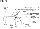
- FIG 10 to FIG 12 shows some further preferred embodiments using above 0.35 micron CMOS technology.
- the Si LED 100 according to FIG 1 couple effectively into a 1 micron thick Si Nitride or polymer waveguide 1800 .
- the Silicon nitride or Si-Oxinitride or polymer based waveguide 1800 coupling is realized on top of the plasma deposited 1802 and field oxide layer 1804 as is normally encountered in above 0.35 micron CMOS technology.
- a further plasma deposited oxide layer 1808 is present, so as to embed the waveguide.
- Appropriate n-well 120 and p+ definitions 130 in the silicon substrate 1806 define the positioning of the light generation Zone at 190 such that optimized coupling of the light is accomplished..
- FIG 11 elaborates on this embodiment by showing a small interface area 1820 realized by means of wet or RF etching such that mechanical, chemical or adsorption process can interfere with the evanescent field as associated with the waveguide , causing excessive optical power loss in the waveguide and subsequent intensity changes.
- a reference optical path A may be realized in parallel to this waveguide in order to ensure as effective reference intensity and signal.
- FIG 12 shows an embodiment of a corresponding CMOS based detector elaborating on this technology.
- the optical detector structure can be realized with a RF pre-etching on the p+ region before deposition of the Silicon nitride layer.
- a p+ n-well based detector is utilized in order to provide an elongated depletion layer , 45 degrees diagonally down into the wafer for above 600nm wavelength . This will provide greater detection efficiency of the detector when using Si nitride or high index polymer waveguides.
- FIG 13 and 14 show preferred embodiments of Si LED and waveguide technology as associated with the technology using below 0.35 micron CMOS technology.
- FIG 13 (a) shows the realization of a lateral enhanced multiplication SI LED as in FIG 1 as realized with appropriate doping layers and embedding techniques.
- the highly doped region 1310 is embedded in a region of lower doping 1320.
- the triangular tip of the highly doped region 1 is such that the light emission zone interfaces with the core of a trench- based optical waveguide 1330 positioned by separate techniques near to the waveguide structure.
- FIG. 13 (b) shows a cross-section of the trench based waveguide.
- the trench is outlined by a thin layer of field oxide or other based silicon oxide 1330.
- a higher refractive index material 1340 is realized inside the trench by means of suitable technology.
- the core region can be of square or circular refractive index profile so as to create either single mode or multimode optical propagation according to usual optical fibre technology.
- FIG. 14 shows a schematic diagram showing achievement of effective coupling of optical radiation from a Lateral Multiplication and Secondary Excitation Si LED into an isolation trench based waveguide structure which can be implemented in below 0.35 micron CMOS technology.
- the isolation trench which is normally used for electrical isolation purposes has been filled by suitable layers of different refractive index material, so as to form an optical waveguide along the trench in a lateral direction.
- FIG 14 shows a further embodiment of the invention in order to enhance the optical coupling from the body 100 structure into the optical conducting body 1092.
- FIG. 14 shows a schematic representation of an embodiment of the generic E-MOD Si LED in order to enhance silicon and optical waveguide interface charge carrier interaction as well as enhancing optical coupling from the Si LED into a lateral positioned waveguide.
- the generic body 100 structure comprising three or four regions 1010 to 1040 are used, but the metal contacts and feeds are such placed on metal layer 1060 that a higher current density is favoured at the surface of second region 1020 and third region 1030, hence maximizing optical yield at the region 1020 and region 1030 surface with the optical fibre core, hence enhancing coupling of the optical radiation 1090 into the higher index core 1096 of the waveguide 1092.
- the respective regions 1010 - 1040 may be embedded into each other and/or placed adjacently to each other in order to create a functional Si LED structure.
- the Electrical contact regions are with normal plasma deposition and etching techniques.
- the wave-guiding secondary optically conductive region could be fabricated by either using isolation trench technology as utilised for below 0.35 micron technology or even polymer technology.
- the higher core refractive index can be fabricated by modifying and trench fabrication technology.
- the encapsulating of the body 100 region can be achieved by first defining the silicon regions 1410 to 1440 by lithographic processes using the topmost silicon layer of the silicon on oxide on insulator structure, and then depositing/growing secondary oxide layers so as to encapsulate the initial body 100.
- the wave-guiding secondary optically conductive region 1094 could be fabricated by using plasma deposition, wet oxide or secondary polymer deposition techniques, such that a strip of low refractive index is generated that contacts the active light emitting regions of the body 1092 region.
- the higher refractive index core regions 1096 can be fabricated by the same procedures, or using techniques and technologies as commonly utilised in the optical fibre telecommunications technology.
- the Electrical contact regions can be fabricated with normal plasma deposition and etching techniques.
- FIG. 15 provides detail of realizing the invention in SOI technology.
- FIG. 15 shows a schematic diagram showing the realization of a MOEMS device as described in FIG. 2 by utilizing Silicon -On - Insulator (SOI) technology as further preferred embodiments of the invention.
- the light emitting diode is fabricated in the silicon layer which is situated on top of the insulating layer. Adjacently in the same layer appropriate optical transparent waveguides are fabricated in a lateral direction which can guide the light away from the Si LED. Secondary optical paths can be generated utilizing optical splitters and also guiding the light out of the plane of the thin silicon layer.
- FIG. 15 shows an embodiment of optical coupling into waveguides utilizing Silicon-On-Insulator technology in cross-sectional view.
- a silicon oxide insulating layer 610 is formed on a silicon substrate 600.
- a silicon layer 620 is present which can also be used for optional further active electronic components, as schematically indicated by reference numeral 640.
- the body 300 is formed on the silicon oxide insulating layer 610 .
- the respective regions 310, 320 330 of body 300 are defined adjacently to each other in order to create a functional Si LED structure.
- the p+nn+ active region is fabricated on the silicon layer 620 of the three layer silicon-on oxide on Si insulator substrate 600.
- the Electrical contact regions 650, 650' and 650" are realized with normal plasma deposition and etching techniques for all terminals T1, T2 and T3 contacting the respective regions 310, 320 330 of body 300.
- a higher core refractive index 660 can be fabricated by modifying and trench fabrication technology.
- the wave-guiding secondary optically conductive region 670 could be fabricated by either using plasma deposition, wet oxide or secondary polymer deposition techniques, such that a strip of low refractive index is generated that contacts the active light emitting regions of the body 300 region, and lying in the plane of the silicon on insulator layer 620.
- the higher refractive index core regions 660 can be fabricated adjacently to the body 300 structure, in the same plane as the silicon layer 620, by the same procedures, or using techniques and technologies as commonly utilized in the optical fibre telecommunications technology, and according to the structural layout concepts.
- the waveguides and electro-optical coupling structures as realized in the embodiments as described above may utilizing either silicon oxide, silicon oxi-nitride, polymer or silicon nitride or combinations of these.
- the waveguides should be of suitable low loss selected, of glassy type.
- the respective regions as in body 300 may be embedded into each other and/or placed adjacently to each other in order to create a functional Si LED structure.
- the Electrical contact regions are with normal plasma deposition and etching techniques.
- the wave-guiding secondary optically conductive region could be fabricated by either using isolation trench technology as utilised for below 0.35 micron technology or even polymer technology.
- the higher core refractive index can be fabricated by modifying overlayers and trench fabrication technology.
- the encapsulating of the body 300 region can be achieved by first defining the silicon regions by lithographic processes using the topmost silicon layer of the silicon on oxide on insulator structure, and then depositing/growing secondary oxide layers so as to encapsulate the initial body region.
- the wave-guiding secondary optically conductive region could be fabricated by either using plasma deposition, wet oxide or secondary polymer deposition techniques, such that a strip of low refractive index is generated that contacts the active light emitting regions of the body region, and lying in the plane of the silicon on insulator layer.
- the higher refractive index core regions can be fabricated by the same procedures, or using techniques and technologies as commonly utilised in the optical fibre telecommunications technology.
- the Electrical contact regions can be fabricated with normal plasma deposition and etching techniques.
- the waveguides and electro-optical coupling structures as realized in the embodiments as described above may utilizing either silicon oxide, silicon oxi-nitride, polymer or silicon nitride or combinations of these.
- the waveguides should be of suitable low loss selected, of glassy type.
- Standard Si p-n and Si p-i-n detector arrangements can be utilized in the invention as detectors.
Landscapes
- Physics & Mathematics (AREA)
- General Physics & Mathematics (AREA)
- Engineering & Computer Science (AREA)
- Chemical & Material Sciences (AREA)
- Life Sciences & Earth Sciences (AREA)
- Pathology (AREA)
- Immunology (AREA)
- General Health & Medical Sciences (AREA)
- Biochemistry (AREA)
- Microelectronics & Electronic Packaging (AREA)
- Analytical Chemistry (AREA)
- Health & Medical Sciences (AREA)
- Plasma & Fusion (AREA)
- Chemical Kinetics & Catalysis (AREA)
- Fluid Mechanics (AREA)
- Optics & Photonics (AREA)
- Power Engineering (AREA)
- Computer Hardware Design (AREA)
- Condensed Matter Physics & Semiconductors (AREA)
- Spectroscopy & Molecular Physics (AREA)
- Optical Integrated Circuits (AREA)
- Photo Coupler, Interrupter, Optical-To-Optical Conversion Devices (AREA)
Abstract
Description
- The present invention relates to a sensor device. More particularly, the invention relates to a CMOS-based micro-optical -electromechanical -sensor (MOEMS) device with silicon light emitting devices, silicon waveguides and silicon detectors being fabricated using current Complementary Metal Oxide Semiconductor (CMOS) technology or Silicon on Insulator (SOI) technology.
- The vast majority of micro-electronic devices are formed in silicon and, over the last several decades, a substantial effort has been directed to refining the reliability and manufacturability of these devices. As a result, silicon-based microelectronic devices have become dependable and inexpensive commodity items. Particularly, Complementary Metal Oxide Semiconductor (CMOS) technology has become a multi-billion industry providing the basis manufacturing technology for nearly 80 % of all electronic commodities to society. Furthermore Silicon -on-Insulator (SOI) technology is regarded as a future basis technology for combining optoelectronics technology with mainstream electronics manufacturing technology.
- To take advantage of the existing silicon-based knowledge and infrastructure, there is a great interest in integrating active optical components into CMOS and SOI silicon technologies.
- Silicon, however, is an indirect band gap semiconductor material which, unlike a direct band gap semiconductor material, has low photon emission efficiency. As a result, silicon is considered a poor source of electroluminescent radiation.
- Although the photon-generation mechanism is not well understood, one source of visible light from silicon is a reverse biased p-n junction under avalanche breakdown conditions.
- Avalanche breakdown occurs when the p-n junction is reverse biased and the electric field across the junction accelerates electrons into having ionizing collisions with the lattice. The ionizing collisions generate,additional electrons which, along with the original electrons, are accelerated into having additional ionizing collisions. As this process continues, the number of electrons increases dramatically, producing a current multiplication effect. Building on this principle, Snyman et al. in "A Dependency of Quantum Efficiency of Silicon CMOS n pp LEDs on Current Density, IEEE Photonics Technology Letters, Vol. 17, No. 10, October 2005, pp 2041-2043", have reported that the efficiency of light emission from silicon in a Silicon Light Emitting Device (Si LED) can be substantially increased by utilizing a reverse biased p-n junction with a wedge-shaped tip that confines the vertical and lateral electric field.
- Sensor devices have been fabricated in discrete packages in order to measure physical parameters such as temperature, mechanical shock, motion, acceleration, rotation, light levels, fluid flow rate, counting of particles in a flow system, fluorescence and absorption of such particles. However these devices often require complex and sophisticated technology.
- Although the sensor device can be formed on a hybrid module, further improvements.of the sensor devices especially to integration and compactness are generally desirable in order to explore new applications of these devices.
What is therefore required is a sensor device which not only offers an easier integration into an existing commercially available manufacturing technology of CMOS, but also one which provides improved performance characteristics. - In MISIAKOS K ET AL: "Monolithic silicon optoelectronic devices for protein and DNA detection", PROCEEDINGS OF SPIE, SPIE, US, vol. 6125, no. 1, 25 January 2006 (2006-01-25), pages 6125 W-1, XP008137217 radiation emitted from a Silicon based LED is coupled into a silicon nitride waveguide.
-
WO 2007/122556 A2 is a hybride sensor device having a Silicon-based light emitting structure an integrated electro-optical mechanical interface structure being capable to sense mechanical deflections and an integrated electronic driving and processing circuitry so as to detect physical parameters such as acceleration. - MULLER R ET AL: "Silicon-compatible waveguides used for an integrated opto-mechanical pressure sensor", OPTICAL MATERIALS, ELSEVIER SCIENCE PUBLISHERS B.V., AMSTERDAM, NL, vol. 17, no. 1-2, 1 June 2001 (2001-06-01), pages 255-258, XP027378200, shows an integrated optical chip for a pressure sensor, but without integrated Si-LED.
-
WO 2010/086798 A1 having a priority date earlier than the date of the present application and being published after the filing date of the present application discloses a sensor device comprising a Silicon-based light emitting structure operating in avalanche breakdown mode, the light emitting structure being a Si-LED and capable of transmitting light having a wavelength higher than 600nm but lower than the absorption edge of silicon at 950 nm through wave guides, an interface module introducing an intensity change or phase change of the transmitted light, a detector for detecting the intensity or phase change and an integrated electronic driving and processing circuitry so as to process the detector output signal so as to sense physical parameters the Silicon-based light emitting structure, the detector and the integrated electronic driving and processing circuitry being integrated on a single chip. - It is an object of the present invention to provide a sensor device.
- According to a first aspect of the invention there is provided a sensor according to
claim 1. - The sensor may be is either Complementary Metal Oxide Semiconductor (CMOS) technology based or Silicon- on- insulator (SOI) based and integrated on a single chip.
- The sensor may further comprise additional optical filters and a reference optical path section so as to increase the sensitivity of the device for measurements.
- The sensor comprises a monolithically integrated wave-guiding system integrated with the silicon light emitting structure on the same chip.
- The wave-guiding system may further comprise Silicon nitride, or silicon-oxinitride or an optically transparent polymer.
- There is also provided a method of creating a silicon LED based sensor wherein: enhanced light emission is created through enhanced secondary excitation processes in the silicon itself; or enhanced light emission is created through enhanced secondary excitation processes in secondary bodies having a high photonic yield and by placing the second body within reach of the secondary body; and utilizing this light emission to sense physical or fluidic change parameters as detected by creating a secondary optical path arrangement which interfaces closely with the environment and creates enhanced detection of the physical changes through either intensity modulation or phase contrast techniques.
- The device utilizes low cost visible light emitters that can be integrated into the system at the chip level at micro-dimensions and that, together with fibre or glass technology and mechanical modules, can provide the measurement of the necessary physical parameter. The key cost competitive advantage in terms of manufacturing costs is achieved with the simplicity of design, simplicity in assembling and in the utilization of low cost integrated circuit integrated LEDs.
- In summary, the CMOS based sensor device according to the invention comprises a body containing, a CMOS silicon-based light emitting device, one or two optical paths, an electro-mechanical or fluidic environmental interface module, a silicon detector and electronic processing circuitry electronic driving and modulation circuitry. The electro-optical module introduces a disturbance or phase shift in a optical path B, which interacts with the reference optical path A and introduces either intensity or phase shift changes at the detector. Correspondingly, physical changes such as vibration, motion, rotation, acceleration as caused by a mechanical vibrating arm, or intensity changes as caused by fluidic gases or liquids can be detected. The device can be highly integrated in a small volume of integrated circuit space utilizing standard Complementary Metal-Oxide Semiconductor (CMOS) integrated or Silicon - on -Insulator (SOI) technology
- The invention will now be described in greater detail by way of example with reference to the following drawings in which:
- FIG. 1
- is a plan view illustrating a p+nn+ version of an Enhanced Lateral Secondary Excitation Si LED in accordance with the present invention.
- FIG. 2
- is a cross-sectional view illustrating an example of a generic Si LED and CMOS technology based Micro-Optical -Mechanical -Sensor in accordance with the present invention.
- FIG.3
- is a schematic diagram showing a hybrid realization the MOEMS device not forming an embodiment of the invention.
- FIG.4
- is a schematic diagram showing a mixed hybrid-monolithic realization the MOEMS device not forming an embodiment of the invention.
- FIG.5
- is a schematic diagram showing a full monolithic realization the MOEMS device as an embodiment of the invention.
- FIG. 6
- shows a schematic diagram showing the typical layers used in CMOS integrated circuit technology.
- FIG. 7
- shows a schematic diagram showing an optical splitting structure by positioning the optical source and utilising CMOS integrated circuit technology.
- FIG. 8
- shows a schematic diagram showing achievement of complete wave-guiding in an optical splitting structure by positioning the optical source and utilising CMOS integrated circuit technology.
- FIG. 9
- shows a schematic diagram showing achievement of effective optical coupling of optical radiation from a Lateral Multiplication and Secondary Excitation Si LED into silicon nitride or other wave-guide layers as situated in the CMOS chip over-layers according to the present invention by utilizing graded index optically transparent layers immediately above the Si LED emission point.
- FIG 10 to FIG 12
- shows some further preferred embodiments using above 0.35 micron CMOS technology.
- FIG 13
- show preferred embodiments of Si LED and waveguide technology as associated with the technology using below 0.35 micron CMOS technology.
- FIG. 14
- shows a schematic diagram showing achievement of effective coupling of optical radiation from a Lateral Multiplication and Secondary Excitation Si LED into an isolation trench based waveguide structure which can be implemented in below 0.35 micron CMOS technology.
- FIG. 15
- shows a schematic diagram showing the realization of a MOEMS device as described in
FIG. 2 by utilizing Silicon -On - Insulator (SOI) technology as further preferred embodiments of the invention. - Making now reference to the drawings, embodiments of the present invention are outlined in more detail.
- Enhanced versions of SiLEDs have recently been developed.
FIG. 1 describes this type of device. Thedevice 100 is constructed comprising a highly dopedsemiconductor region 120, with an elongated triangle andsharp point protrusion 122. This structure is placed in asemiconductor region 110 of lower doping which is sufficiently large to accommodate the maximum extended depletion region extending from theregion 120 upon reverse bias along the junction periphery (junction ohmic contact regions 130 are placed in the first, opposite and directly parallel to the maximum protrusion body length. The device is appropriately voltage biased such as to create an elongated depletion region along theperiphery 140 of the second body junction towards the electrical contact body regions. Charge carriers as excited in the maximum electric field region near to the junction (p+n junction inFIG 1 ) interface, now will accelerate and transverse not perpendicular to the junction interface, but will rather laterally traverse laterally along thejunction Fig. 1 . Since the depletion region (up to the edge 160) is much more extended as compared to a normally oriented depletion region, the accelerated carriers will now traverse a much longer path before exiting the junction at the end of the depletion region. During their traverse path, they will undergo multiple mean free acceleration paths, each ending in a collision and ionization process of host lattice crystal atoms, defects, impurities, and or other carriers. During these interaction processes light photons are emitted, leading to a particular increase in the total light emission level from the device. It follows that the longer lateral trajectory paths, results in enhanced scattering and multiple mean free paths. This leads to an enhanced avalanche in multiplication of secondary carriers; an exponential increase in further accelerated carriers and an exponential increase in total light emission from the junction. The multiplication region is indicated byreference numeral 180, leading to a dominantlight emission region 170. The excited carriers create secondary carriers that again cause new excitations and new light emission processes within the silicon itself. - By choosing the primary semiconductor body material and conductivity types of the respective bodies, and using the fact that at the multiplication and avalanching of electrons are roughly twice for that of holes in silicon, the concentration and the type of energetic carriers can be engineered. p+ n n+ type arrangement are therefore particularly suitable for yielding high intensity CMOS based LEDs.
- Consequently, appropriate secondary bodies can also be placed within reach of the excited carriers so as to create light emission from either the primary or secondary excited carriers. These Si LEDs were appropriately designated as "secondary excitation Si LEDs". The structure of the device is relatively simple and can be fabricated with ease utilizing CMOS technology. A preferred positioning of such secondary bodies is shown as 190 in
FIG 1 .FIG 2 shows an example overview and cross-sectional view of a Si LED basedCMOS MOEMS device 200 showing various sub-components in accordance with the current invention, and utilizing the SiLEDs. Using conventional CMOS fabrication technology, a Silicon Light Emitting Device (Si LED) 100 is fabricated. Appropriate driving andmodulation circuitry 210 controls the optical output of the device in terms of intensity and pulse width of the LED The optical emission is (optionally) filtered usingoptical filter 220 in order to ensure a narrow bandwidth. The optical emission is guided along suitable optical paths A and B by means of directional emission or wave-guiding technology, using optical intensity splitting and wave-guiding techniques. Path A is used as a reference path with respect to phase and intensity, while path B is transmitted through an electro-mechanical interface orfluidic interface module 230, which introduces an intensity and/or phase change to the optical beam. This module is located either subsurface of the CMOS over-layers or it interfaces with the CMOS chip surface. The two beams is combined in beam section C, where it is fed to a siliconoptical detector 240. The signal output from the detector is processed by means of appropriatesignal processing circuitry 250, and then delivered in analogue or digital format to the rest of the CMOS circuitry which can successfully interpret the signal and information in terms of a physical parameter as measured. - The electro-mechanical sensor interface section is designed such that it detects mechanical vibration, motion, rotation, acceleration and introduces an intensity or phase change to optical path B. Similarly, if a fluidic interface module is used to interface either with a gas or liquid fluid, and accordingly introduces an intensity change, a phase change or a wavelength change to the optical beam in path B. The system can accordingly be utilized to sense mechanical parameters such as vibration, motion, rotation, acceleration, gas flow, gas composition or liquid flow or liquid composition. The whole arrangement is fabricated as a highly integrated module in a small section of CMOS chip. Since the system uses optical means of detection and processing, it has all the advantages as associated with optical signal processing techniques, such as highly miniaturized system, highly integrated manufacturing, low cost of manufacturing, noise immunity, and high reliability.
- The electro-mechanical interface module may utilize state of the art cantilever, micro-beam deflection or disc rotation techniques. The fluidic interface module may utilize state of the art gas or fluid absorption monitoring or wave-length spectrum detection techniques utilizing optical sources and optical sensors.
- The novel component of the device/ arrangement is the Si LED that can be integrated into the silicon subsurface (or the chip over-layers) and that provides sufficient optical power such that the detectors can detect the optical changes as introduced by the mechanical or fluidic interface module with a sufficient signal to noise ratio, such that information can be processed and outputted to adjacent circuitry.
-
FIGS 3 ,4 describe examples not forming embodiments of the invention.FIG. 5 describes a preferred embodiment of the invention. -
FIG.3 is a schematic diagram showing a hybrid realization the MOEMS device not forming an embodiment of the invention, utilizing a mechanical module, an optical module as fabricated in a recess cavity on a CMOS chip hosting the Si LED, optical detection circuitry and appropriate driving and signal processing circuitry.FIG 3 describes an example not forming an embodiment of the invention fabricating a recess in the CMOS over-layers, and adding various optical and mechanical modules such that a total system is realized using hybrid component and hybrid component assembling means, involving Pick and Placing of components into the recess cavity in a CMOS chip. -
FIG 3 describes an example not forming an embodiment of the invention using hybrid approach of the invention. The device consist of three separate modules or bodies viz a semiconductor chip module B1, an optical module or body B2 and a mechanical module or body B3, relative to each other as shown inFig. 4 . An integrated (or embedded) light emitting diode, LED, emits light of a narrow bandwidth into the recess cavity, C1, facilitated previously in the CMOS over layers. Rays impact on a partially reflecting surface RS1. A certain percentage intensity of these rays are reflected to the integrated (or embedded) detector, DET. Another percentage of the light is refracted into optical body B2 body and follows internal reflection paths R3 as indicated inFig 3 . At the partially reflecting surface RS2, a percentage of the light is reflected back to the chip interface according to light rays path R6. Emitting from the optical body after further refraction as, the externally reflected light interferes with the initially reflected light R2 and cause intensity change in the light reaching the detector DET. Another percentage of light at partially refracted at RS2 enters the n3 refraction index region of the optical body B2, and emits normally to this body, then travels through a second cavity C2, is reflected back at reflecting surface RS3. A percentage of this reflected light returns back into the optical body B2 and contribute to phase contrast and intensity change at the detector DET. - If the mechanical arm position changes status, the path length imposed by rays R4 and R5 will cause an intensity change in the detector. Shock, motion, acceleration or rotation of the device will all impose position changes of reflecting surface RS3 and results in intensity changes detected at the detector DET. By extending the air gap path into the secondary cavity environment, intensity changes can be detected at the detector due to various status changes in this cavity e.g. if fluid flows introduced through the cavity C2. The arm can be appropriately modified to detect fluid flow rate. If particles of high optical absorption flow through cavity C2, this will impose sharp changes in the intensity transmitted through C2 which will enable particle counts by the processing circuitry. Similarly, other properties such as absorption and fluorescence as caused by the particles can accordingly impose changes on the intensity as detected by the detector. The signals at the detector is appropriately electronically analyzed and processed for suitable interpretation by micro-processor circuitry.
-
FIG.4 is a schematic diagram showing a mixed hybrid-monolithic realization the MOEMS device not forming an embodiment of the invention, utilizing a mechanical module, as fabricated in a recess cavity on a CMOS chip hosting the Si LED, optical detection circuitry and appropriate driving and signal processing circuitry. The optical filter and reference optical path can either be hybridly added to surface of the CMOS chip or it can be monolithically fabricated as an integral part of the CMOS chip.FIG. 4 describes a second example not forming an embodiment of invention using hybridly added mechanical or fluidic interface unit into a recess cavity into a CMOS chip; and either using a hybridly added optical filter and second optical paths. -
FIG 4 gives an example not forming an embodiment of the invention using a mixed -hybrid monolithic approach. A recess is manufactured such that thechip surface 400 is sufficiently exposed so as the emit light vertically out of the chip at either a vertical or slanted direction. An appropriateoptical filter 220 is fabricated at the chip-recess interface such that only a narrow bandwidth in wavelength of the optical emission ofSiLED 100 is transmitted into therecess cavity 410. The electro-mechanical orfluidic interface module 230 is located inside the recess cavity, or partially inside therecess cavity 410 or totally outside the recess cavity. Theoptical filter 220 may be fabricated using monolithic layer fabrication technology, or it may be pick- and- placed positioned separately into the cavity. - The optical radiation following path A towards and back from the electromechanical or
fluidic interface module 230 is of narrow bandwidth or monochromatic nature which will enhance phase contrast and eventually contribute towards enhanced intensity changes as detected by the detector. An optional optical path A may be fabricated utilizing monolithic, waveguide basted or other hybrid techniques. This addition may enhance the phase contrast and intensity changes at thedetector 240 as a result of changes introduced by the electro-mechanical or fluidic interface module. -
FIG. 5 describes a completely monolithic embodiment of the invention utilizing all CMOS fabrication technology.FIG.5 is a schematic diagram showing a full monolithic realization theMOEMS device 500 as a preferred embodiment of the invention, utilizing a mechanical module, as fabricated in a recess cavity on a CMOS chip. TheSi LED 100, the wave-guiding circuitry, filtering components and phase contrast enhancement components are all fabricated monolithically as an integral part of the CMOS chip. - A large area silicon light emitting device supplies sufficient optical power to a monolithically integrated wave guiding system on the chip or section thereof. The optical power is transferred to the waveguides through an appropriate
optical coupler 510. The coupled optical radiation in the fibre is then filtered by either a Bragg grating filter 520 or (optional) ring resonator filter 530 (or any other state of the art wave-guiding filtering means) such that a very narrow band radiation (as close to mono-chromatic as possible) is obtained. The optical radiation is then split into two waveguide paths, path A and path B, as in an un-balanced MachZender phase detector 540. In the optical path B, the optical radiation is exposed to the electro-mechanical orfluidic interface module 230, which introduces a phase change according to the selected physical detection parameter. This phase change causes a resulting intensity change in the final optical path C before it is fed into theoptical detector 240. -
FIGS. 6 to 8 describe various beam directing, optical spitting and wave-guiding techniques that can be used in the optical paths A, B and C. -
FIG. 6 shows a schematic diagram showing the typical layers used in CMOS integrated circuit technology viz (1) the optically transparent SiO2 field oxide layer, (2) the inter-metallic plasma deposited oxide layers; and (3) the silicon nitride (Si3N4) passivation layer. Two optional optical emission points, A and B, are shown in the CMOS chip and the focusing and directional emission properties of the structure are illustrated. -
Fig. 6 shows the schematic diagram showing the typical layers as used in CMOS integrated circuit technology for optical application purposes. The optically transparent layers are SiO2 field oxide layer, silicon nitride (Si3N4) passivation layer and inter-metallic plasma deposited oxide layers which are all deposited as over-layers on the silicon substrate. In this case a small section of field oxide is fabricated using above 0.35 micron CMOS technology, so as to create a curvature in the overlying plasma oxide and silicon nitride layers. The lateral length of the structure was reduced and the position of the optical source was placed at an optimized point at the silicon substrate-field oxide interface in the centre of the structure. The optical launch angles for the rays were chosen in the range, 30°- 150°. The design can be implemented to include a circular nature of the centre field oxide region. When the source is placed at position A, a clear focusing of almost all rays emitting vertically from the structure is observed. The focusing and beam directional changes are caused by the change in refractive indexes of the various layers viz 1.4 for silicon oxide, 1.55 for silicon plasma oxide and 2.4 for silicon nitride. - When the source is placed at position B, a clear directional emission of the radiation towards a slanted 45 degree angle is observed, also with some focusing or converging of optical rays present.
-
FIG. 7 shows a schematic diagram showing an optical splitting structure by positioning the optical source at position, C, in CMOS integrated circuit technology. The layer definitions are the same as inFIG.6. FIG 7 demonstrates a structure that can be used to create optical splitting of the optically radiated power in more or less equal percentages in two different paths. In this case a 0.3 micron field oxide layer and 1 micron silicon passivation and plasma deposited layers were assumed as commonly encountered in 0.35 micron CMOS technology. One portion of the radiation emitted out of the structure into air, and the other radiation was emitted laterally into the silicon nitride layer. -
FIG. 8 shows a schematic diagram showing achievement of complete wave-guiding in an optical splitting structure by positioning the optical source at position, D, in CMOS integrated circuit technology. The layer definitions are the same as inFIG.6 .FIG. 8 demonstrates optimized lateral wave-guiding longitudinally along the silicon nitride layer for a very high proportion of the totally emitted Si LED radiation. The plasma oxide layer thickness has been reduced locally and the optical emission point in the generated structure is positioned near the "bird beak" point in the silicon oxide layer. The initial rays launch angles ranging from 34°-76° couple effectively into the silicon nitride layer. Due to the lower refractive indexes of both the plasma and field oxide below the layer and the refractive index of air above the layer, the radiation is effectively guided along the silicon nitride layer. - A very important aspect related to the invention is that silicon nitride and silicon oxi-nitride is essentially transparent for radiation for radiation higher than 600nm. This is substantially lower than the absorption edge of silicon which lies at approximately 850-950 nm which imply that the radiation can still be effectively detected using standard CMOS detector technology. Silicon nitride therefore offers itself as a most suitable candidate for generating electro-optic and waveguide structures in CMOS integrated circuitry. If longer wavelength Si LEDs are used as optical sources, it implies that an "all-silicon" wave-guiding and MOEMS systems can be very effectively realized in CMOS technology.
-
FIGS 9 and10 describe details of optical coupling technology from the Si LED to the optical paths A, B and C. -
FIG. 9 shows a schematic diagram showing achievement of effective optical coupling of optical radiation according to the present invention from a Lateral Multiplication and Secondary Excitation Si LED into silicon nitride or other wave-guide layers as situated in the CMOS chip over-layers, by utilizing graded index optically transparent layers immediately above the Si LED emission point.FIG. 9 shows an embodiment for coupling of optical radiation as emitted from theSi LED 100 into a laterally positionedwaveguide 900. - A window is wet-etched or dry-etched above the Si CMOS LED
light emitting region 920, having dimensions in the micron range. This is followed by appropriately masking the rest of the plan view of the CMOS chip with a mask and then depositingvarious layers 910 of graded index in the cavity. If the choice of grading is chosen correct, in this case from low to high as one progress from the Si-SiO2 interface towards the surface, refraction of light may be generated in two dimensions such that the emitted light is focused into the core of any single mode or multimode optical fibre, with a very good coupling coefficient. - A
depletion layer 930, acarrier excitation region 940 are part of theSi LED 100, as well assecond region 120,electric contact region 960 andoxide insulating layer 980, similar to the devices as described with respect to the previous embodiments. - In further embodiments, different over-layers may be deposited through masks using the same graded index concepts and definition of the optical index gradient both laterally and vertically in the over-layer, such that a series of optical graded index waveguides are formed in the over-layers of conventional CMOS integrated circuitry, by employing appropriate post-processing procedures. In further embodiments different over-layers may be deposited through masks using the same graded index concepts and definition of the optical index gradient both laterally and vertically in the over-layer, such that a series of optical graded index waveguides are formed directly on top of the insulating layer, normally the field oxide layer of CMOS IC's, such that a region of higher refractive index are formed directly above the field oxide layer, and such that a conventional rib waveguide or single or multimode mode high index fibre/waveguide are formed, and such that the emission from the Si CMOS LED effectively couple into the higher index part of the waveguide. The detail process and choice of materials can be chosen in order to optimize the technology. If necessary, optical layers may be pre-deposited before metal layers are deposited which are normally require a low thermal budget and are accommodated at the end of the CMOS processing procedure. The graded index composition can also be obtained with conventional glass doping and glass flow techniques. If necessary, certain dedicated optical modules can be separately fabricated using different processes, and pick and placed into position together with pick and placing of fibre optical modules after CMOS processing, and as a post processing procedure. All these embodiments are usually suitable for implementation with above 0.35 micron CMOS technology.
-
FIG 10 to FIG 12 shows some further preferred embodiments using above 0.35 micron CMOS technology. - In
FIG 10 theSi LED 100 according toFIG 1 couple effectively into a 1 micron thick Si Nitride orpolymer waveguide 1800 . The Silicon nitride or Si-Oxinitride or polymer basedwaveguide 1800 coupling is realized on top of the plasma deposited 1802 andfield oxide layer 1804 as is normally encountered in above 0.35 micron CMOS technology. Above thewaveguide 1800, a further plasma depositedoxide layer 1808 is present, so as to embed the waveguide. Appropriate n-well 120 andp+ definitions 130 in thesilicon substrate 1806 define the positioning of the light generation Zone at 190 such that optimized coupling of the light is accomplished.. -
FIG 11 elaborates on this embodiment by showing a small interface area 1820 realized by means of wet or RF etching such that mechanical, chemical or adsorption process can interfere with the evanescent field as associated with the waveguide , causing excessive optical power loss in the waveguide and subsequent intensity changes. A reference optical path A may be realized in parallel to this waveguide in order to ensure as effective reference intensity and signal.. -
FIG 12 shows an embodiment of a corresponding CMOS based detector elaborating on this technology. The optical detector structure can be realized with a RF pre-etching on the p+ region before deposition of the Silicon nitride layer. A p+ n-well based detector is utilized in order to provide an elongated depletion layer , 45 degrees diagonally down into the wafer for above 600nm wavelength . This will provide greater detection efficiency of the detector when using Si nitride or high index polymer waveguides. -
FIG 13 and14 and show preferred embodiments of Si LED and waveguide technology as associated with the technology using below 0.35 micron CMOS technology. -
FIG 13 (a) shows the realization of a lateral enhanced multiplication SI LED as inFIG 1 as realized with appropriate doping layers and embedding techniques. The highly dopedregion 1310 is embedded in a region of lower doping 1320. The triangular tip of the highly dopedregion 1 is such that the light emission zone interfaces with the core of a trench- based optical waveguide 1330 positioned by separate techniques near to the waveguide structure.FIG. 13 (b) shows a cross-section of the trench based waveguide. The trench is outlined by a thin layer of field oxide or other based silicon oxide 1330. A higherrefractive index material 1340 is realized inside the trench by means of suitable technology. The core region can be of square or circular refractive index profile so as to create either single mode or multimode optical propagation according to usual optical fibre technology. -
FIG. 14 shows a schematic diagram showing achievement of effective coupling of optical radiation from a Lateral Multiplication and Secondary Excitation Si LED into an isolation trench based waveguide structure which can be implemented in below 0.35 micron CMOS technology. The isolation trench which is normally used for electrical isolation purposes has been filled by suitable layers of different refractive index material, so as to form an optical waveguide along the trench in a lateral direction.FIG 14 shows a further embodiment of the invention in order to enhance the optical coupling from thebody 100 structure into theoptical conducting body 1092.FIG. 14 shows a schematic representation of an embodiment of the generic E-MOD Si LED in order to enhance silicon and optical waveguide interface charge carrier interaction as well as enhancing optical coupling from the Si LED into a lateral positioned waveguide. Here thegeneric body 100 structure comprising three or fourregions 1010 to 1040 are used, but the metal contacts and feeds are such placed onmetal layer 1060 that a higher current density is favoured at the surface of second region 1020 andthird region 1030, hence maximizing optical yield at the region 1020 andregion 1030 surface with the optical fibre core, hence enhancing coupling of theoptical radiation 1090 into thehigher index core 1096 of thewaveguide 1092. - Here the respective regions 1010 - 1040 may be embedded into each other and/or placed adjacently to each other in order to create a functional Si LED structure. The Electrical contact regions are with normal plasma deposition and etching techniques. The wave-guiding secondary optically conductive region could be fabricated by either using isolation trench technology as utilised for below 0.35 micron technology or even polymer technology. The higher core refractive index can be fabricated by modifying and trench fabrication technology. The encapsulating of the
body 100 region can be achieved by first defining the silicon regions 1410 to 1440 by lithographic processes using the topmost silicon layer of the silicon on oxide on insulator structure, and then depositing/growing secondary oxide layers so as to encapsulate theinitial body 100. The wave-guiding secondary opticallyconductive region 1094 could be fabricated by using plasma deposition, wet oxide or secondary polymer deposition techniques, such that a strip of low refractive index is generated that contacts the active light emitting regions of thebody 1092 region. The higher refractiveindex core regions 1096 can be fabricated by the same procedures, or using techniques and technologies as commonly utilised in the optical fibre telecommunications technology. The Electrical contact regions can be fabricated with normal plasma deposition and etching techniques. -
FIG. 15 provides detail of realizing the invention in SOI technology.
FIG. 15 shows a schematic diagram showing the realization of a MOEMS device as described inFIG. 2 by utilizing Silicon -On - Insulator (SOI) technology as further preferred embodiments of the invention. The light emitting diode is fabricated in the silicon layer which is situated on top of the insulating layer. Adjacently in the same layer appropriate optical transparent waveguides are fabricated in a lateral direction which can guide the light away from the Si LED. Secondary optical paths can be generated utilizing optical splitters and also guiding the light out of the plane of the thin silicon layer. -
FIG. 15 shows an embodiment of optical coupling into waveguides utilizing Silicon-On-Insulator technology in cross-sectional view. On asilicon substrate 600, a siliconoxide insulating layer 610 is formed. Above the silicon oxide insulating layer 610 asilicon layer 620 is present which can also be used for optional further active electronic components, as schematically indicated byreference numeral 640. On the siliconoxide insulating layer 610 thebody 300 is formed. Here therespective regions body 300 are defined adjacently to each other in order to create a functional Si LED structure. The p+nn+ active region is fabricated on thesilicon layer 620 of the three layer silicon-on oxide onSi insulator substrate 600. TheElectrical contact regions respective regions body 300. - A higher core
refractive index 660 can be fabricated by modifying and trench fabrication technology. The wave-guiding secondary opticallyconductive region 670 could be fabricated by either using plasma deposition, wet oxide or secondary polymer deposition techniques, such that a strip of low refractive index is generated that contacts the active light emitting regions of thebody 300 region, and lying in the plane of the silicon oninsulator layer 620. The higher refractiveindex core regions 660 can be fabricated adjacently to thebody 300 structure, in the same plane as thesilicon layer 620, by the same procedures, or using techniques and technologies as commonly utilized in the optical fibre telecommunications technology, and according to the structural layout concepts. The waveguides and electro-optical coupling structures as realized in the embodiments as described above may utilizing either silicon oxide, silicon oxi-nitride, polymer or silicon nitride or combinations of these. The waveguides should be of suitable low loss selected, of glassy type. - As shown in
FIG. 15 , the respective regions as inbody 300 may be embedded into each other and/or placed adjacently to each other in order to create a functional Si LED structure. The Electrical contact regions are with normal plasma deposition and etching techniques. The wave-guiding secondary optically conductive region could be fabricated by either using isolation trench technology as utilised for below 0.35 micron technology or even polymer technology. The higher core refractive index can be fabricated by modifying overlayers and trench fabrication technology. The encapsulating of thebody 300 region can be achieved by first defining the silicon regions by lithographic processes using the topmost silicon layer of the silicon on oxide on insulator structure, and then depositing/growing secondary oxide layers so as to encapsulate the initial body region. The wave-guiding secondary optically conductive region could be fabricated by either using plasma deposition, wet oxide or secondary polymer deposition techniques, such that a strip of low refractive index is generated that contacts the active light emitting regions of the body region, and lying in the plane of the silicon on insulator layer. The higher refractive index core regions can be fabricated by the same procedures, or using techniques and technologies as commonly utilised in the optical fibre telecommunications technology. The Electrical contact regions can be fabricated with normal plasma deposition and etching techniques. - The waveguides and electro-optical coupling structures as realized in the embodiments as described above may utilizing either silicon oxide, silicon oxi-nitride, polymer or silicon nitride or combinations of these. The waveguides should be of suitable low loss selected, of glassy type.
- Standard Si p-n and Si p-i-n detector arrangements can be utilized in the invention as detectors.
- Although certain embodiments only have been described herein, it will be readily apparent to any person skilled in the art that other modifications and/or variations of the invention are possible.
Claims (12)
- A sensor device comprising:• a Silicon-based light emitting structure operating in avalanche breakdown mode, the light emitting structure being a SiLED (100) and capable of transmitting light having a wavelength higher than 600nm but lower than the absorption edge of silicon at 950 nm;• an optical coupling module (510, 410) being configured to couple optical radiation from the SiLED (100) into wave guides (900) by utilizing graded index optically transparent layers (910) immediately above the Si LED (100) emission point (920);• an interface module (230) introducing an intensity change and/or phase change of the transmitted light;• a detector (240) for detecting the intensity and/or phase change; and• an integrated electronic driving and processing circuitry (210, 250) so as to process the detector (240) output signal, so as to sense parameters such as vibration, motion, rotation, acceleration, gas flow, gas composition or liquid flow or liquid composition or to detect optical absorption, additional wavelength added or omitted elements in gaseous or fluidic samples, wherein the Silicon-based light emitting structure (100), the detector (240) and the integrated electronic driving and processing circuitry (210, 250) are integrated on a single chip.
- The sensor according to claim 1, which is either Complementary Metal Oxide Semiconductor (CMOS) technology based or Silicon- on- insulator (SOI) based.
- The sensor according to claim 1 or 2, further comprising additional optical filters (220) and/or a reference optical path section (A) so as to increase the sensitivity of the device for the sense parameters.
- The sensor according to any of claims 1 to 3, wherein light of the Silicon-based light emitting structure (100) is emitted directional.
- The sensor according to any of claims 1 to 4, further comprising a monolithically integrated wave-guiding system (900) integrated with the silicon light emitting structure (100) on the same chip.
- The sensor according to claim 5, wherein the wave-guiding system (900) comprises a plurality of transparent layers with graded refractive indices.
- The sensor according to claim 5, wherein the wave-guiding system (900) comprises a trench in the substrate being outlined by a thin layer of oxide and a higher refractive index material, which can be of square or circular refractive index profile so as to create either single mode or multimode optical propagation.
- The sensor according to claim 7, wherein the trench is an isolation trench in a below 0.35 µm CMOS technology.
- The sensor according to any of claims 5 to 8, wherein the wave-guiding system (900) comprising Silicon nitride, or silicon-oxinitride or an optically transparent polymer.
- The sensor according to any of claims 1 to 9, wherein by utilizing Silicon -On - Insulator (SOI) technology, the wave-guiding system (900) with a strip of low refractive index material is generated that contacts the active light emitting region and is lying in the plane of the silicon on insulator layer.
- The sensor according to any of claims 1 to 10, wherein the light emitting structure (100) comprises a lateral enhanced multiplication Sl LED having a highly doped region which is embedded in a region of lower doping and having a triangular tip such that a light emission zone interfaces with a core of a trench- based optical waveguide.
- The sensor according to any of claims 1 to 11, wherein the detector (240) is a p+n-well based detector with an elongated depletion layer, which is 45 degrees diagonally down into the wafer for above 600nm wavelength detection.
Applications Claiming Priority (10)
| Application Number | Priority Date | Filing Date | Title |
|---|---|---|---|
| ZA200904163 | 2009-06-15 | ||
| ZA200904162 | 2009-06-15 | ||
| ZA200904509 | 2009-06-26 | ||
| ZA200904665 | 2009-07-03 | ||
| ZA200904666 | 2009-07-03 | ||
| ZA200905249 | 2009-07-28 | ||
| ZA200908834 | 2009-12-11 | ||
| ZA201003603 | 2010-05-21 | ||
| ZA201003605 | 2010-05-21 | ||
| PCT/ZA2010/000033 WO2011038423A2 (en) | 2009-06-15 | 2010-06-15 | Cmos moems sensor device |
Publications (2)
| Publication Number | Publication Date |
|---|---|
| EP2443465A2 EP2443465A2 (en) | 2012-04-25 |
| EP2443465B1 true EP2443465B1 (en) | 2013-12-25 |
Family
ID=43796539
Family Applications (1)
| Application Number | Title | Priority Date | Filing Date |
|---|---|---|---|
| EP10819670.0A Not-in-force EP2443465B1 (en) | 2009-06-15 | 2010-06-15 | Cmos moems sensor device |
Country Status (6)
| Country | Link |
|---|---|
| US (1) | US9435822B2 (en) |
| EP (1) | EP2443465B1 (en) |
| KR (1) | KR101415648B1 (en) |
| CN (1) | CN102483427B (en) |
| WO (1) | WO2011038423A2 (en) |
| ZA (1) | ZA201108938B (en) |
Families Citing this family (15)
| Publication number | Priority date | Publication date | Assignee | Title |
|---|---|---|---|---|
| US8260098B1 (en) * | 2011-02-17 | 2012-09-04 | Nxp B.V. | Optocoupler circuit |
| DE102012019407A1 (en) * | 2012-10-04 | 2014-04-10 | Leoni Kabel Holding Gmbh | Optical sensor arrangement and method for detecting a measured variable with the aid of an optical sensor arrangement |
| DE102013201217A1 (en) * | 2013-01-25 | 2014-07-31 | Osram Opto Semiconductors Gmbh | Organic optoelectronic component has organic light emitting element that emits light which is radiated internally to transparent outer layer and is routed to organic light-detecting element |
| CN103604785A (en) * | 2013-11-05 | 2014-02-26 | 浙江工业大学 | Fluorescence detection system |
| JP2017520764A (en) | 2014-06-09 | 2017-07-27 | エスティーシー. ユーエヌエムStc.Unm | Integrated bound mode spectrum / angle sensor |
| US11480463B2 (en) | 2014-06-09 | 2022-10-25 | Unm Rainforest Innovations | Integrated bound-mode spectral/angular sensors |
| DE102015000064B3 (en) * | 2015-01-12 | 2016-03-31 | Carl Von Ossietzky Universität Oldenburg | Apparatus and method for determining at least one parameter of a flow of a fluid and its use |
| US9874693B2 (en) | 2015-06-10 | 2018-01-23 | The Research Foundation For The State University Of New York | Method and structure for integrating photonics with CMOs |
| CN106403821A (en) * | 2015-07-27 | 2017-02-15 | 中国科学院苏州纳米技术与纳米仿生研究所 | Displacement sensor, usage and manufacturing method thereof and interferometer |
| CN108475685A (en) * | 2016-06-02 | 2018-08-31 | 歌尔股份有限公司 | Monolithic integrated device and micro-total analysis system |
| CN106597012A (en) * | 2017-01-18 | 2017-04-26 | 中北大学 | Accelerometer based on light intensity modulation type MOEMS |
| CN108333123A (en) * | 2018-02-08 | 2018-07-27 | 南京邮电大学 | A kind of CMOS spectrometers based on MIM guide technologies |
| CN108279320B (en) * | 2018-02-09 | 2020-12-04 | 中北大学 | Preparation method of nano optical waveguide accelerometer based on Fano resonance |
| CN111214209B (en) * | 2018-11-27 | 2024-01-09 | 晶元光电股份有限公司 | Optical sensing module |
| CN112285380B (en) * | 2020-10-20 | 2022-03-18 | 合肥工业大学 | Optical MEMS acceleration sensor and preparation method thereof |
Family Cites Families (8)
| Publication number | Priority date | Publication date | Assignee | Title |
|---|---|---|---|---|
| US5017010A (en) * | 1989-05-16 | 1991-05-21 | International Business Machines Corporation | High sensitivity position sensor and method |
| US5917180A (en) * | 1997-07-16 | 1999-06-29 | Canadian Space Agency | Pressure sensor based on illumination of a deformable integrating cavity |
| EP1748290A1 (en) * | 2005-07-28 | 2007-01-31 | Fondazione Torino Wireless | A device and a system for measuring forces |
| WO2007122556A2 (en) | 2006-04-21 | 2007-11-01 | Koninklijke Philips Electronics N.V. | Detection circuit for detecting movements of a movable object |
| WO2008146276A1 (en) * | 2007-05-31 | 2008-12-04 | S.A.E Afikim | System and method for analyzing fluids |
| US20120224167A1 (en) * | 2007-07-18 | 2012-09-06 | Honeywell International, Inc. | Apparatus and method for chemical, biological and radiological agent sensing |
| US7989822B2 (en) * | 2007-11-08 | 2011-08-02 | Eugene R. Worley | Optocoupler using silicon based LEDs |
| WO2010086798A1 (en) | 2009-01-27 | 2010-08-05 | Insiava (Pty) Limited | Microchip-based moems and waveguide device |
-
2010
- 2010-06-15 WO PCT/ZA2010/000033 patent/WO2011038423A2/en active Application Filing
- 2010-06-15 US US13/378,234 patent/US9435822B2/en not_active Expired - Fee Related
- 2010-06-15 KR KR1020127000910A patent/KR101415648B1/en not_active IP Right Cessation
- 2010-06-15 CN CN201080036174.3A patent/CN102483427B/en not_active Expired - Fee Related
- 2010-06-15 EP EP10819670.0A patent/EP2443465B1/en not_active Not-in-force
-
2011
- 2011-12-06 ZA ZA2011/08938A patent/ZA201108938B/en unknown
Non-Patent Citations (2)
| Title |
|---|
| MISIAKOS K ET AL: "Monolithic silicon optoelectronic devices for protein and DNA detection", PROCEEDINGS OF SPIE, SPIE, US, vol. 6125, no. 1, 25 January 2006 (2006-01-25), pages 6125W - 1, XP008137217, ISSN: 0277-786X, [retrieved on 20060301], DOI: 10.1117/12.644687 * |
| MULLER R ET AL: "Silicon-compatible waveguides used for an integrated opto-mechanical pressure sensor", OPTICAL MATERIALS, ELSEVIER SCIENCE PUBLISHERS B.V. AMSTERDAM, NL, vol. 17, no. 1-2, 1 June 2001 (2001-06-01), pages 255 - 258, XP027378200, ISSN: 0925-3467, [retrieved on 20010601] * |
Also Published As
| Publication number | Publication date |
|---|---|
| ZA201108938B (en) | 2014-05-28 |
| CN102483427A (en) | 2012-05-30 |
| WO2011038423A2 (en) | 2011-03-31 |
| WO2011038423A3 (en) | 2011-10-20 |
| KR101415648B1 (en) | 2014-08-06 |
| EP2443465A2 (en) | 2012-04-25 |
| US9435822B2 (en) | 2016-09-06 |
| KR20120040189A (en) | 2012-04-26 |
| CN102483427B (en) | 2014-11-26 |
| US20120154812A1 (en) | 2012-06-21 |
Similar Documents
| Publication | Publication Date | Title |
|---|---|---|
| EP2443465B1 (en) | Cmos moems sensor device | |
| US8395226B2 (en) | Microchip-based MOEMS and waveguide device | |
| KR100853067B1 (en) | Photodiode and method for manufacturing same | |
| US8848194B2 (en) | Integrated plasmonic nanocavity sensing device | |
| US8359904B2 (en) | Photoacoustic gas detector | |
| EP3607291B1 (en) | Hermeticity testing of an optical assembly | |
| US20170276870A1 (en) | Cmos based micro-photonic systems | |
| US10222294B2 (en) | Wafer level testing of optical devices | |
| JP2009531736A (en) | Coupled light to microresonator | |
| US20090028487A1 (en) | Micro-ring optical detector/modulator | |
| US20090180748A1 (en) | Ridge Waveguide | |
| CN111665211A (en) | Gas sensor | |
| US20120153864A1 (en) | Wavelength specific silicon light emitting structure | |
| CN114222911A (en) | Optical nanostructure suppressor for integrated devices and methods thereof | |
| CN111727367A (en) | Chemical sensing device using fluorescent sensing material | |
| JP4018603B2 (en) | Optical waveguide sensor | |
| KR101316596B1 (en) | AN ALL SILICON 750 nm AND CMOS-BASED OPTICAL COMMUNICATION SYSTEM UTILIZING MOD-E AVALANCHE LEDs | |
| JP5581955B2 (en) | Minute substance detection sensor and minute substance detection apparatus having the same | |
| JPWO2019107133A1 (en) | Optical waveguide and optical density measuring device | |
| US11340401B2 (en) | Optical circuit for alignment and optical alignment method | |
| US20240222542A1 (en) | Photodetector apparatus and method of detecting light | |
| Izquierdo et al. | Silicon nanocrystals light-emitting devices: characterization and coupling to SU-8 waveguides | |
| Zimmermann et al. | Integrated Optics | |
| JP2017215273A (en) | Fluorescence sensor |
Legal Events
| Date | Code | Title | Description |
|---|---|---|---|
| PUAI | Public reference made under article 153(3) epc to a published international application that has entered the european phase |
Free format text: ORIGINAL CODE: 0009012 |
|
| 17P | Request for examination filed |
Effective date: 20120116 |
|
| AK | Designated contracting states |
Kind code of ref document: A2 Designated state(s): AL AT BE BG CH CY CZ DE DK EE ES FI FR GB GR HR HU IE IS IT LI LT LU LV MC MK MT NL NO PL PT RO SE SI SK SM TR |
|
| DAX | Request for extension of the european patent (deleted) | ||
| 17Q | First examination report despatched |
Effective date: 20130102 |
|
| RIC1 | Information provided on ipc code assigned before grant |
Ipc: G01N 21/64 20060101ALI20130731BHEP Ipc: G01N 21/77 20060101ALI20130731BHEP Ipc: H01L 33/34 20100101ALI20130731BHEP Ipc: G02B 6/42 20060101ALI20130731BHEP Ipc: G01F 1/28 20060101ALI20130731BHEP Ipc: H01L 27/15 20060101ALI20130731BHEP Ipc: G02B 6/12 20060101ALI20130731BHEP Ipc: G01D 5/26 20060101ALI20130731BHEP Ipc: G02B 6/35 20060101ALI20130731BHEP Ipc: G01P 15/093 20060101AFI20130731BHEP Ipc: G01N 21/25 20060101ALI20130731BHEP |
|
| GRAP | Despatch of communication of intention to grant a patent |
Free format text: ORIGINAL CODE: EPIDOSNIGR1 |
|
| RIC1 | Information provided on ipc code assigned before grant |
Ipc: G01F 1/28 20060101ALI20130913BHEP Ipc: G01N 21/77 20060101ALI20130913BHEP Ipc: G02B 6/12 20060101ALI20130913BHEP Ipc: H01L 33/34 20100101ALI20130913BHEP Ipc: G02B 6/35 20060101ALI20130913BHEP Ipc: G01P 15/093 20060101AFI20130913BHEP Ipc: G01N 21/25 20060101ALI20130913BHEP Ipc: G01N 21/64 20060101ALI20130913BHEP Ipc: G01D 5/26 20060101ALI20130913BHEP Ipc: G02B 6/42 20060101ALI20130913BHEP Ipc: H01L 27/15 20060101ALI20130913BHEP |
|
| INTG | Intention to grant announced |
Effective date: 20131001 |
|
| GRAS | Grant fee paid |
Free format text: ORIGINAL CODE: EPIDOSNIGR3 |
|
| GRAA | (expected) grant |
Free format text: ORIGINAL CODE: 0009210 |
|
| AK | Designated contracting states |
Kind code of ref document: B1 Designated state(s): AL AT BE BG CH CY CZ DE DK EE ES FI FR GB GR HR HU IE IS IT LI LT LU LV MC MK MT NL NO PL PT RO SE SI SK SM TR |
|
| REG | Reference to a national code |
Ref country code: GB Ref legal event code: FG4D |
|
| REG | Reference to a national code |
Ref country code: CH Ref legal event code: EP |
|
| REG | Reference to a national code |
Ref country code: AT Ref legal event code: REF Ref document number: 646879 Country of ref document: AT Kind code of ref document: T Effective date: 20140115 |
|
| REG | Reference to a national code |
Ref country code: IE Ref legal event code: FG4D |
|
| REG | Reference to a national code |
Ref country code: DE Ref legal event code: R096 Ref document number: 602010012767 Country of ref document: DE Effective date: 20140220 |
|
| PG25 | Lapsed in a contracting state [announced via postgrant information from national office to epo] |
Ref country code: FI Free format text: LAPSE BECAUSE OF FAILURE TO SUBMIT A TRANSLATION OF THE DESCRIPTION OR TO PAY THE FEE WITHIN THE PRESCRIBED TIME-LIMIT Effective date: 20131225 Ref country code: SE Free format text: LAPSE BECAUSE OF FAILURE TO SUBMIT A TRANSLATION OF THE DESCRIPTION OR TO PAY THE FEE WITHIN THE PRESCRIBED TIME-LIMIT Effective date: 20131225 Ref country code: LT Free format text: LAPSE BECAUSE OF FAILURE TO SUBMIT A TRANSLATION OF THE DESCRIPTION OR TO PAY THE FEE WITHIN THE PRESCRIBED TIME-LIMIT Effective date: 20131225 Ref country code: HR Free format text: LAPSE BECAUSE OF FAILURE TO SUBMIT A TRANSLATION OF THE DESCRIPTION OR TO PAY THE FEE WITHIN THE PRESCRIBED TIME-LIMIT Effective date: 20131225 Ref country code: NO Free format text: LAPSE BECAUSE OF FAILURE TO SUBMIT A TRANSLATION OF THE DESCRIPTION OR TO PAY THE FEE WITHIN THE PRESCRIBED TIME-LIMIT Effective date: 20140325 |
|
| REG | Reference to a national code |
Ref country code: NL Ref legal event code: VDEP Effective date: 20131225 |
|
| REG | Reference to a national code |
Ref country code: AT Ref legal event code: MK05 Ref document number: 646879 Country of ref document: AT Kind code of ref document: T Effective date: 20131225 |
|
| REG | Reference to a national code |
Ref country code: LT Ref legal event code: MG4D |
|
| PG25 | Lapsed in a contracting state [announced via postgrant information from national office to epo] |
Ref country code: LV Free format text: LAPSE BECAUSE OF FAILURE TO SUBMIT A TRANSLATION OF THE DESCRIPTION OR TO PAY THE FEE WITHIN THE PRESCRIBED TIME-LIMIT Effective date: 20131225 |
|
| PG25 | Lapsed in a contracting state [announced via postgrant information from national office to epo] |
Ref country code: EE Free format text: LAPSE BECAUSE OF FAILURE TO SUBMIT A TRANSLATION OF THE DESCRIPTION OR TO PAY THE FEE WITHIN THE PRESCRIBED TIME-LIMIT Effective date: 20131225 Ref country code: IS Free format text: LAPSE BECAUSE OF FAILURE TO SUBMIT A TRANSLATION OF THE DESCRIPTION OR TO PAY THE FEE WITHIN THE PRESCRIBED TIME-LIMIT Effective date: 20140425 Ref country code: BE Free format text: LAPSE BECAUSE OF FAILURE TO SUBMIT A TRANSLATION OF THE DESCRIPTION OR TO PAY THE FEE WITHIN THE PRESCRIBED TIME-LIMIT Effective date: 20131225 |
|
| PG25 | Lapsed in a contracting state [announced via postgrant information from national office to epo] |
Ref country code: AT Free format text: LAPSE BECAUSE OF FAILURE TO SUBMIT A TRANSLATION OF THE DESCRIPTION OR TO PAY THE FEE WITHIN THE PRESCRIBED TIME-LIMIT Effective date: 20131225 Ref country code: SK Free format text: LAPSE BECAUSE OF FAILURE TO SUBMIT A TRANSLATION OF THE DESCRIPTION OR TO PAY THE FEE WITHIN THE PRESCRIBED TIME-LIMIT Effective date: 20131225 Ref country code: CY Free format text: LAPSE BECAUSE OF FAILURE TO SUBMIT A TRANSLATION OF THE DESCRIPTION OR TO PAY THE FEE WITHIN THE PRESCRIBED TIME-LIMIT Effective date: 20131225 Ref country code: CZ Free format text: LAPSE BECAUSE OF FAILURE TO SUBMIT A TRANSLATION OF THE DESCRIPTION OR TO PAY THE FEE WITHIN THE PRESCRIBED TIME-LIMIT Effective date: 20131225 Ref country code: ES Free format text: LAPSE BECAUSE OF FAILURE TO SUBMIT A TRANSLATION OF THE DESCRIPTION OR TO PAY THE FEE WITHIN THE PRESCRIBED TIME-LIMIT Effective date: 20131225 Ref country code: NL Free format text: LAPSE BECAUSE OF FAILURE TO SUBMIT A TRANSLATION OF THE DESCRIPTION OR TO PAY THE FEE WITHIN THE PRESCRIBED TIME-LIMIT Effective date: 20131225 Ref country code: RO Free format text: LAPSE BECAUSE OF FAILURE TO SUBMIT A TRANSLATION OF THE DESCRIPTION OR TO PAY THE FEE WITHIN THE PRESCRIBED TIME-LIMIT Effective date: 20131225 Ref country code: PT Free format text: LAPSE BECAUSE OF FAILURE TO SUBMIT A TRANSLATION OF THE DESCRIPTION OR TO PAY THE FEE WITHIN THE PRESCRIBED TIME-LIMIT Effective date: 20140428 |
|
| REG | Reference to a national code |
Ref country code: DE Ref legal event code: R097 Ref document number: 602010012767 Country of ref document: DE |
|
| PG25 | Lapsed in a contracting state [announced via postgrant information from national office to epo] |
Ref country code: DK Free format text: LAPSE BECAUSE OF FAILURE TO SUBMIT A TRANSLATION OF THE DESCRIPTION OR TO PAY THE FEE WITHIN THE PRESCRIBED TIME-LIMIT Effective date: 20131225 |
|
| PLBE | No opposition filed within time limit |
Free format text: ORIGINAL CODE: 0009261 |
|
| STAA | Information on the status of an ep patent application or granted ep patent |
Free format text: STATUS: NO OPPOSITION FILED WITHIN TIME LIMIT |
|
| PG25 | Lapsed in a contracting state [announced via postgrant information from national office to epo] |
Ref country code: PL Free format text: LAPSE BECAUSE OF FAILURE TO SUBMIT A TRANSLATION OF THE DESCRIPTION OR TO PAY THE FEE WITHIN THE PRESCRIBED TIME-LIMIT Effective date: 20131225 |
|
| 26N | No opposition filed |
Effective date: 20140926 |
|
| REG | Reference to a national code |
Ref country code: DE Ref legal event code: R097 Ref document number: 602010012767 Country of ref document: DE Effective date: 20140926 |
|
| PG25 | Lapsed in a contracting state [announced via postgrant information from national office to epo] |
Ref country code: LU Free format text: LAPSE BECAUSE OF FAILURE TO SUBMIT A TRANSLATION OF THE DESCRIPTION OR TO PAY THE FEE WITHIN THE PRESCRIBED TIME-LIMIT Effective date: 20140615 Ref country code: MC Free format text: LAPSE BECAUSE OF FAILURE TO SUBMIT A TRANSLATION OF THE DESCRIPTION OR TO PAY THE FEE WITHIN THE PRESCRIBED TIME-LIMIT Effective date: 20131225 |
|
| REG | Reference to a national code |
Ref country code: CH Ref legal event code: PL |
|
| REG | Reference to a national code |
Ref country code: IE Ref legal event code: MM4A |
|
| PG25 | Lapsed in a contracting state [announced via postgrant information from national office to epo] |
Ref country code: LI Free format text: LAPSE BECAUSE OF NON-PAYMENT OF DUE FEES Effective date: 20140630 Ref country code: CH Free format text: LAPSE BECAUSE OF NON-PAYMENT OF DUE FEES Effective date: 20140630 Ref country code: IE Free format text: LAPSE BECAUSE OF NON-PAYMENT OF DUE FEES Effective date: 20140615 |
|
| PG25 | Lapsed in a contracting state [announced via postgrant information from national office to epo] |
Ref country code: SI Free format text: LAPSE BECAUSE OF FAILURE TO SUBMIT A TRANSLATION OF THE DESCRIPTION OR TO PAY THE FEE WITHIN THE PRESCRIBED TIME-LIMIT Effective date: 20131225 |
|
| PG25 | Lapsed in a contracting state [announced via postgrant information from national office to epo] |
Ref country code: MT Free format text: LAPSE BECAUSE OF FAILURE TO SUBMIT A TRANSLATION OF THE DESCRIPTION OR TO PAY THE FEE WITHIN THE PRESCRIBED TIME-LIMIT Effective date: 20131225 |
|
| PG25 | Lapsed in a contracting state [announced via postgrant information from national office to epo] |
Ref country code: SM Free format text: LAPSE BECAUSE OF FAILURE TO SUBMIT A TRANSLATION OF THE DESCRIPTION OR TO PAY THE FEE WITHIN THE PRESCRIBED TIME-LIMIT Effective date: 20131225 |
|
| REG | Reference to a national code |
Ref country code: FR Ref legal event code: PLFP Year of fee payment: 7 |
|
| PG25 | Lapsed in a contracting state [announced via postgrant information from national office to epo] |
Ref country code: GR Free format text: LAPSE BECAUSE OF FAILURE TO SUBMIT A TRANSLATION OF THE DESCRIPTION OR TO PAY THE FEE WITHIN THE PRESCRIBED TIME-LIMIT Effective date: 20140326 Ref country code: BG Free format text: LAPSE BECAUSE OF FAILURE TO SUBMIT A TRANSLATION OF THE DESCRIPTION OR TO PAY THE FEE WITHIN THE PRESCRIBED TIME-LIMIT Effective date: 20131225 Ref country code: IT Free format text: LAPSE BECAUSE OF FAILURE TO SUBMIT A TRANSLATION OF THE DESCRIPTION OR TO PAY THE FEE WITHIN THE PRESCRIBED TIME-LIMIT Effective date: 20131225 |
|
| PG25 | Lapsed in a contracting state [announced via postgrant information from national office to epo] |
Ref country code: TR Free format text: LAPSE BECAUSE OF FAILURE TO SUBMIT A TRANSLATION OF THE DESCRIPTION OR TO PAY THE FEE WITHIN THE PRESCRIBED TIME-LIMIT Effective date: 20131225 Ref country code: HU Free format text: LAPSE BECAUSE OF FAILURE TO SUBMIT A TRANSLATION OF THE DESCRIPTION OR TO PAY THE FEE WITHIN THE PRESCRIBED TIME-LIMIT; INVALID AB INITIO Effective date: 20100615 |
|
| PGFP | Annual fee paid to national office [announced via postgrant information from national office to epo] |
Ref country code: GB Payment date: 20160628 Year of fee payment: 7 |
|
| PGFP | Annual fee paid to national office [announced via postgrant information from national office to epo] |
Ref country code: FR Payment date: 20160621 Year of fee payment: 7 |
|
| PGFP | Annual fee paid to national office [announced via postgrant information from national office to epo] |
Ref country code: DE Payment date: 20160630 Year of fee payment: 7 |
|
| REG | Reference to a national code |
Ref country code: DE Ref legal event code: R119 Ref document number: 602010012767 Country of ref document: DE |
|
| GBPC | Gb: european patent ceased through non-payment of renewal fee |
Effective date: 20170615 |
|
| REG | Reference to a national code |
Ref country code: FR Ref legal event code: ST Effective date: 20180228 |
|
| PG25 | Lapsed in a contracting state [announced via postgrant information from national office to epo] |
Ref country code: DE Free format text: LAPSE BECAUSE OF NON-PAYMENT OF DUE FEES Effective date: 20180103 Ref country code: GB Free format text: LAPSE BECAUSE OF NON-PAYMENT OF DUE FEES Effective date: 20170615 |
|
| PG25 | Lapsed in a contracting state [announced via postgrant information from national office to epo] |
Ref country code: FR Free format text: LAPSE BECAUSE OF NON-PAYMENT OF DUE FEES Effective date: 20170630 |
|
| PG25 | Lapsed in a contracting state [announced via postgrant information from national office to epo] |
Ref country code: MK Free format text: LAPSE BECAUSE OF FAILURE TO SUBMIT A TRANSLATION OF THE DESCRIPTION OR TO PAY THE FEE WITHIN THE PRESCRIBED TIME-LIMIT Effective date: 20131225 |
|
| PG25 | Lapsed in a contracting state [announced via postgrant information from national office to epo] |
Ref country code: AL Free format text: LAPSE BECAUSE OF FAILURE TO SUBMIT A TRANSLATION OF THE DESCRIPTION OR TO PAY THE FEE WITHIN THE PRESCRIBED TIME-LIMIT Effective date: 20131225 |