EP2441580A1 - LC panel compensators - Google Patents
LC panel compensators Download PDFInfo
- Publication number
- EP2441580A1 EP2441580A1 EP12150510A EP12150510A EP2441580A1 EP 2441580 A1 EP2441580 A1 EP 2441580A1 EP 12150510 A EP12150510 A EP 12150510A EP 12150510 A EP12150510 A EP 12150510A EP 2441580 A1 EP2441580 A1 EP 2441580A1
- Authority
- EP
- European Patent Office
- Prior art keywords
- cos
- sin
- panel
- plane
- retardance
- Prior art date
- Legal status (The legal status is an assumption and is not a legal conclusion. Google has not performed a legal analysis and makes no representation as to the accuracy of the status listed.)
- Ceased
Links
Images
Classifications
-
- G—PHYSICS
- G02—OPTICS
- G02F—OPTICAL DEVICES OR ARRANGEMENTS FOR THE CONTROL OF LIGHT BY MODIFICATION OF THE OPTICAL PROPERTIES OF THE MEDIA OF THE ELEMENTS INVOLVED THEREIN; NON-LINEAR OPTICS; FREQUENCY-CHANGING OF LIGHT; OPTICAL LOGIC ELEMENTS; OPTICAL ANALOGUE/DIGITAL CONVERTERS
- G02F1/00—Devices or arrangements for the control of the intensity, colour, phase, polarisation or direction of light arriving from an independent light source, e.g. switching, gating or modulating; Non-linear optics
- G02F1/01—Devices or arrangements for the control of the intensity, colour, phase, polarisation or direction of light arriving from an independent light source, e.g. switching, gating or modulating; Non-linear optics for the control of the intensity, phase, polarisation or colour
- G02F1/13—Devices or arrangements for the control of the intensity, colour, phase, polarisation or direction of light arriving from an independent light source, e.g. switching, gating or modulating; Non-linear optics for the control of the intensity, phase, polarisation or colour based on liquid crystals, e.g. single liquid crystal display cells
- G02F1/133—Constructional arrangements; Operation of liquid crystal cells; Circuit arrangements
- G02F1/1333—Constructional arrangements; Manufacturing methods
- G02F1/1335—Structural association of cells with optical devices, e.g. polarisers or reflectors
- G02F1/13363—Birefringent elements, e.g. for optical compensation
- G02F1/133634—Birefringent elements, e.g. for optical compensation the refractive index Nz perpendicular to the element surface being different from in-plane refractive indices Nx and Ny, e.g. biaxial or with normal optical axis
-
- G—PHYSICS
- G02—OPTICS
- G02F—OPTICAL DEVICES OR ARRANGEMENTS FOR THE CONTROL OF LIGHT BY MODIFICATION OF THE OPTICAL PROPERTIES OF THE MEDIA OF THE ELEMENTS INVOLVED THEREIN; NON-LINEAR OPTICS; FREQUENCY-CHANGING OF LIGHT; OPTICAL LOGIC ELEMENTS; OPTICAL ANALOGUE/DIGITAL CONVERTERS
- G02F1/00—Devices or arrangements for the control of the intensity, colour, phase, polarisation or direction of light arriving from an independent light source, e.g. switching, gating or modulating; Non-linear optics
- G02F1/01—Devices or arrangements for the control of the intensity, colour, phase, polarisation or direction of light arriving from an independent light source, e.g. switching, gating or modulating; Non-linear optics for the control of the intensity, phase, polarisation or colour
- G02F1/13—Devices or arrangements for the control of the intensity, colour, phase, polarisation or direction of light arriving from an independent light source, e.g. switching, gating or modulating; Non-linear optics for the control of the intensity, phase, polarisation or colour based on liquid crystals, e.g. single liquid crystal display cells
- G02F1/133—Constructional arrangements; Operation of liquid crystal cells; Circuit arrangements
- G02F1/1333—Constructional arrangements; Manufacturing methods
- G02F1/1335—Structural association of cells with optical devices, e.g. polarisers or reflectors
- G02F1/13363—Birefringent elements, e.g. for optical compensation
- G02F1/133637—Birefringent elements, e.g. for optical compensation characterised by the wavelength dispersion
-
- G—PHYSICS
- G02—OPTICS
- G02F—OPTICAL DEVICES OR ARRANGEMENTS FOR THE CONTROL OF LIGHT BY MODIFICATION OF THE OPTICAL PROPERTIES OF THE MEDIA OF THE ELEMENTS INVOLVED THEREIN; NON-LINEAR OPTICS; FREQUENCY-CHANGING OF LIGHT; OPTICAL LOGIC ELEMENTS; OPTICAL ANALOGUE/DIGITAL CONVERTERS
- G02F1/00—Devices or arrangements for the control of the intensity, colour, phase, polarisation or direction of light arriving from an independent light source, e.g. switching, gating or modulating; Non-linear optics
- G02F1/01—Devices or arrangements for the control of the intensity, colour, phase, polarisation or direction of light arriving from an independent light source, e.g. switching, gating or modulating; Non-linear optics for the control of the intensity, phase, polarisation or colour
- G02F1/13—Devices or arrangements for the control of the intensity, colour, phase, polarisation or direction of light arriving from an independent light source, e.g. switching, gating or modulating; Non-linear optics for the control of the intensity, phase, polarisation or colour based on liquid crystals, e.g. single liquid crystal display cells
- G02F1/133—Constructional arrangements; Operation of liquid crystal cells; Circuit arrangements
- G02F1/136—Liquid crystal cells structurally associated with a semi-conducting layer or substrate, e.g. cells forming part of an integrated circuit
- G02F1/1362—Active matrix addressed cells
- G02F1/136277—Active matrix addressed cells formed on a semiconductor substrate, e.g. of silicon
-
- G—PHYSICS
- G02—OPTICS
- G02F—OPTICAL DEVICES OR ARRANGEMENTS FOR THE CONTROL OF LIGHT BY MODIFICATION OF THE OPTICAL PROPERTIES OF THE MEDIA OF THE ELEMENTS INVOLVED THEREIN; NON-LINEAR OPTICS; FREQUENCY-CHANGING OF LIGHT; OPTICAL LOGIC ELEMENTS; OPTICAL ANALOGUE/DIGITAL CONVERTERS
- G02F2203/00—Function characteristic
- G02F2203/02—Function characteristic reflective
-
- G—PHYSICS
- G02—OPTICS
- G02F—OPTICAL DEVICES OR ARRANGEMENTS FOR THE CONTROL OF LIGHT BY MODIFICATION OF THE OPTICAL PROPERTIES OF THE MEDIA OF THE ELEMENTS INVOLVED THEREIN; NON-LINEAR OPTICS; FREQUENCY-CHANGING OF LIGHT; OPTICAL LOGIC ELEMENTS; OPTICAL ANALOGUE/DIGITAL CONVERTERS
- G02F2413/00—Indexing scheme related to G02F1/13363, i.e. to birefringent elements, e.g. for optical compensation, characterised by the number, position, orientation or value of the compensation plates
- G02F2413/04—Number of plates greater than or equal to 4
-
- G—PHYSICS
- G02—OPTICS
- G02F—OPTICAL DEVICES OR ARRANGEMENTS FOR THE CONTROL OF LIGHT BY MODIFICATION OF THE OPTICAL PROPERTIES OF THE MEDIA OF THE ELEMENTS INVOLVED THEREIN; NON-LINEAR OPTICS; FREQUENCY-CHANGING OF LIGHT; OPTICAL LOGIC ELEMENTS; OPTICAL ANALOGUE/DIGITAL CONVERTERS
- G02F2413/00—Indexing scheme related to G02F1/13363, i.e. to birefringent elements, e.g. for optical compensation, characterised by the number, position, orientation or value of the compensation plates
- G02F2413/08—Indexing scheme related to G02F1/13363, i.e. to birefringent elements, e.g. for optical compensation, characterised by the number, position, orientation or value of the compensation plates with a particular optical axis orientation
-
- G—PHYSICS
- G02—OPTICS
- G02F—OPTICAL DEVICES OR ARRANGEMENTS FOR THE CONTROL OF LIGHT BY MODIFICATION OF THE OPTICAL PROPERTIES OF THE MEDIA OF THE ELEMENTS INVOLVED THEREIN; NON-LINEAR OPTICS; FREQUENCY-CHANGING OF LIGHT; OPTICAL LOGIC ELEMENTS; OPTICAL ANALOGUE/DIGITAL CONVERTERS
- G02F2413/00—Indexing scheme related to G02F1/13363, i.e. to birefringent elements, e.g. for optical compensation, characterised by the number, position, orientation or value of the compensation plates
- G02F2413/10—Indexing scheme related to G02F1/13363, i.e. to birefringent elements, e.g. for optical compensation, characterised by the number, position, orientation or value of the compensation plates with refractive index ellipsoid inclined, or tilted, relative to the LC-layer surface O plate
-
- G—PHYSICS
- G02—OPTICS
- G02F—OPTICAL DEVICES OR ARRANGEMENTS FOR THE CONTROL OF LIGHT BY MODIFICATION OF THE OPTICAL PROPERTIES OF THE MEDIA OF THE ELEMENTS INVOLVED THEREIN; NON-LINEAR OPTICS; FREQUENCY-CHANGING OF LIGHT; OPTICAL LOGIC ELEMENTS; OPTICAL ANALOGUE/DIGITAL CONVERTERS
- G02F2413/00—Indexing scheme related to G02F1/13363, i.e. to birefringent elements, e.g. for optical compensation, characterised by the number, position, orientation or value of the compensation plates
- G02F2413/12—Biaxial compensators
-
- G—PHYSICS
- G02—OPTICS
- G02F—OPTICAL DEVICES OR ARRANGEMENTS FOR THE CONTROL OF LIGHT BY MODIFICATION OF THE OPTICAL PROPERTIES OF THE MEDIA OF THE ELEMENTS INVOLVED THEREIN; NON-LINEAR OPTICS; FREQUENCY-CHANGING OF LIGHT; OPTICAL LOGIC ELEMENTS; OPTICAL ANALOGUE/DIGITAL CONVERTERS
- G02F2413/00—Indexing scheme related to G02F1/13363, i.e. to birefringent elements, e.g. for optical compensation, characterised by the number, position, orientation or value of the compensation plates
- G02F2413/13—Positive birefingence
Definitions
- Disclosed embodiments herein relate to optical devices for use in liquid crystal (LC) display systems, and more particularly to reflective liquid crystal on silicon (LCoS) projection architectures that require panel-only compensation.
- These embodiments represent optical components that consist of one or more birefringent layers that compensate for residual in-plane and out-of-plane retardation present in the OFF-state of an LC panel.
- these components typically demand high durability and high polarization performance, and as such a low-elasticity organic substrate is preferred, as described in the preceding provisional U.S. Patent Application No. 60/573,910 , which is hereby incorporated by reference herein.
- compensators act first to remove residual in-plane OFF-state retardance of the panel, and second to reduce OFF-state light leakage due to the out-of-plane retardance which relates to field-of-view (FOV) performance of the LC layer.
- Removing the in-plane retardance is important, as it affects all incident light, since it corresponds to the extent to which the LC molecules are not aligned normal to the substrate or not balanced in their orientations when projected onto the panel plane.
- the substantial out-of-plane retardance alters the polarization state of off-axis rays, and acts to reduce the panel's field-of-view and in non-collimated systems leads again to OFF-state leakage.
- both in-plane and out-of-plane compensation is desired.
- FIGURES 1a-b are optical block diagram of exemplary compensator and LC panel arrangements, showing for background purposes relative arrangement and orientations of compensators relative to LC panels;
- FIGURE 2 is a graph of optimal compensator optic axis orientation as a function of net in-plane retardance for compensating an exemplary 3 nm residual vertically aligned LCOS panel;
- FIGURE 3 illustrates a first embodiment compensator comprising separate a-plate and c-plate compensators
- FIGURE 4 illustrates a second embodiment compensator in which a single biaxial compensator is used to compensate for an LC panel
- FIGURE 5 is a graph illustrating the insensitivity of biaxial out-of-plane retardance for different in-plane compensation values
- FIGURE 6 illustrates a further embodiment compensator in which a single c-plate is tilted to provide in-plane compensation
- FIGURE 7 illustrates a bi-layer compensator embodiment for compensating LC reflective panels
- FIGURE 8 shows the optimum average retardance value for a crossed a-plate compensator as a function of in-plane retardance, again for an exemplary 3 nm residual vertically aligned LCOS panel;
- FIGURE 9 illustrates a compensator constructed in accordance with disclosed manufacturing techniques
- FIGURE 10 illustrates an unfolded bi-layer compensated transmissive system
- FIGURE 11 illustrates a transmissive system based on the bi-layer reflective system in which the compensator pairs are placed on one side of the panel and combined into a single compensator;
- FIGURES 12a-b are exemplary field-of-view diagrams showing respectively the FOV at 550 nm of an uncompensated transmissive homeotropic aligned LC panel and one that is compensated using the approach of FIGURE 11 .
- Certain disclosed compensation schemes may be used in reflective systems where the input/output beam separating PBSs do not require additional compensation (e.g., wire grid PBSs) or are compensated separately.
- Such systems provide that a linear polarization state exists prior to the system analyzer. Specifically, dark state light exiting the input/output beam-separating PBSs has the same linear polarization state as the light entering as a result of the orthogonal analyzing and polarization axes.
- the output analyzer orientation is independent of the polarizer and allows for compensation solutions that produce rotated linear output states.
- each birefringent layer or the collection of birefringent layers can exhibit uniaxial or biaxial properties.
- Specific cases include a- and c-plate combinations, single biaxial films, tilted c-plates, and bi-layer compensators comprising two uniaxial layers having their optic axes oriented substantially orthogonally with respect to each other. Compensation of transmissive panels can be achieved by related methods and are also covered by the general methodology of this patent by 'unfolding' reflective designs.
- a stretched organic film may be used as the birefringent layer or layers in the described embodiments. To avoid degradation within the harsh environment of a projection system, compensators using these stretched organic films may be formed as an encapsulated laminate.
- An exemplary effective organic film is a low-elasticity polyolefin film.
- FIGURES 1a -b are optical block diagrams illustrating relative layouts and orientations of compensators relative to LC panels (comprising LC layers and reflectors) that they are compensating.
- FIGURE 1a shows an optical system 100 comprising a compensator 102.
- Polarized light 103 impinges on the compensator 102, and is shown with a linear (vertical polarization).
- the compensator 102 has a certain optic axis orientation and in-plane retardance, theta r and gamma r, respectively, where theta r is the orientation angle relative to the linear polarization of the polarized input light 103.
- the compensator imparts an elliptical polarization 105 to the light 103 incident on the LC layer 104.
- the elliptical polarization is configured such that it will compensate for the built-in residual in-plane retardance of the LC layer 104, such that the output from the LC layer 104 will be linearly polarized as it impinges upon the reflection plane 106.
- this process occurs in the reverse order, and the compensator 102 has been configured such that the output light 103 (along the same path as the input light) has the same linear polarization as the input light.
- the optical system 100 of FIGURE 1b operates in the same way as the optical system 100 of FIGURE 1a , except that in FIGURE 1b the compensator 102 is positioned between the LC panel 104 and the reflector 106, whereas in FIGURE 1a it was positioned optically ahead of both of those elements.
- the compensator 102 of either FIGURE 1a or FIGURE 1b can accordingly be configured to compensate for the elliptical polarization imparted in the OFF-state by the LC panel 104, whether the compensator 102 is located between the LC panel 104 and reflector 106, as in FIGURE 1b , or optically before both of those elements, as in FIGURE 1a .
- FIGURE 1b is also a useful approximation for the more-common architecture of FIGURE 1a , and that approximation holds particularly for small in-plane panel 104/106 and compensator 102 retardances.
- the less conventional arrangement of FIGURE 1b therefore simplifies the matrix mathematics described below, and accordingly is also described herein. But, as mentioned, the matrix mathematics also accurately describe the more conventional arrangement of FIGURE 1a for small in-plane panel 104/106 and compensator 102 retardances.
- FIGURES 1a-b provides a background for understanding the developments and advancement of the present application, which includes specific approaches in which LC panels 104 can be compensated by compensating residual OFF-state in-plane retardance together with compensating off-axis polarization mixing caused by the panel's OFF-state out-of-plane retardance. In certain embodiments, this may be viewed as a sequential, two-step process as light passes through the system. But while there may be certain advantages in the order of compensation, and certain statements in the specification may seem to imply a certain order, the use of the described embodiments should not be construed to limit the scope of the claims. The claims alone may require certain orders or sequences of compensation, and as such only those claims specifically spelling out particular orders of compensation should be construed to be so limited.
- the LC panel includes both an LC material 104 and a reflective plane 106.
- the described embodiment involves first the matching and then negating the in-plane retardance of compensator (gamma r) and panel (gamma p).
- exact matching of the retardances is not necessary, and in fact may be undesirable.
- the system specifically can be configured to compensate for the retardance mismatch between the compensator and the panel by changing the relative orientations between the panel 104/106 and the compensators 102.
- the compensation for the retardance mismatch can only be achieved where the compensator's 102 in-plane retardance exceeds the in-plane component of the panel's 104/106 dark-state retardance.
- the present application describes the compensators 102 as being positioned outside the panels 104/106, it is also possible to place the compensators 102 'within' reflective panels 104/106, as is shown in FIGURE 1b .
- the compensator is interposed between the LC material 104 and the reflective plane 106.
- this application recognizes the advantage of having a substantial mismatch between compensator and panel retardances. Certain embodiments of this application accordingly describe approaches or designs that work effectively with the substantial mismatch in compensator and panel retardances.
- in-plane retardance mismatch which is the difference between the panel's OFF-state in-plane residual retardance and the compensator's in-plane retardance
- resulting optimal compensating orientation can be determined mathematically as is described herein.
- f and e are the conventional orientation and ellipticity angles describing the polarized state transformed from the input polarization by the LC layer 104.
- Gamma r and theta r are the in-plane retardance and orientation of the compensator 102, and lambda is the wavelength of the compensated light.
- the output polarization is linear if it is orthogonal to the vector (0 0 1), hence the scalar product can be equated to zero in Equation 1.
- Equation 1 can be solved to give the following expression relating compensator orientation as a function of retardance:
- ⁇ ⁇ r ⁇ r 1 2 ⁇ asin tan 2 ⁇ ⁇ tan 2 ⁇ ⁇ r ⁇ ⁇ ⁇ - ⁇
- FIGURE 2 illustrates a resulting 'C' curve 202 of optimal compensator orientation (y-axis) as a function of in-plane retardance (x-axis) for the above Equation 2 when the residual retardance is 3 nm at an input wavelength of 550 nm.
- gamma r > gamma p
- the in-plane retardance is shown as an example at gamma r approx. equal 7 nm, which yields theta 1 approx. equal 15° and theta 2 approx. equal 75°, and given the relatively flat slope of the C-curve 200 in this region, the solution would be relatively impervious to variations in the in-plane retardance values of the compensator 102 and/or LC panel 104/106.
- the flatter part of the C-curve exists in some of the described embodiments for gamma r - gamma p > approximately 15 nm.
- Moving away from the 45° solution 205 to other portions of the illustrated C-curve 200 provides better systemic tolerance of variations of retardance values, gamma r and gamma p, thereby improving the manufacturability of the optical systems in which the disclosed compensators are employed.
- An exemplary solution range would be in those solutions on the C-curve where the orientation angle theta is less than approximately 20° and the orientation angle theta is greater than approximately 70° (e.g., in those areas where the C-curve 200 is flattening out).
- a wider angle range would be where the orientation angle theta 1 is less than approximately 30° and the orientation angle theta is greater than approximately 60°.
- the solutions closer to the 45° solution 205 have the disadvantage of requiring tighter tolerance on the in-plane retardance values in order to maintain the same the optical system components near their optimal orientations.
- Equation 1 describes solutions whereby the in-plane residual retardance of a panel gamma p can be compensated in a reflective LC projection system by an optical component that has an in-plane retardance gamma r equal to, or greater than, gamma r.
- in-plane compensation only may yield sufficient system performance, a more complete solution requires simultaneous out-of-plane panel compensation.
- the embodiments of this patent therefore consist of creating a compensating component that has one or more birefringent layers that has an in-plane retardance value greater than that of the panel and properties that can offer some (or indeed complete) out-of-plane compensation. This component can then be oriented in accordance with Equation 1 to ensure good in-plane compensation.
- FIGURE 3 illustrates a system designed to compensate an LC panel's in-plane residual and out-of-plane retardance components.
- the retardance projected onto the plane normal to each ray's propagation direction by the LC layer's out-of-plane retardance must be subtracted. This is conventionally done by introducing negative birefringent plates whose optic axes are normal to the mean optical propagation. These birefringent plates are known as 'c-plates,' and they are set with retardances roughly matching the entire retardance of the panels being compensated (Dn ⁇ d ⁇ 250nm).
- FIGURE 3 illustrates one approach that attacks both in-plane and out-of-plane OFF-state LC panel compensation.
- This approach comprises a two-layer compensator 300 comprising an in-plane uniaxial compensator (a-plate) 302 complying with the 'head-on' criteria of Equation 2 and a c-plate 304.
- Conventional compensator solutions of this general structure are known. But known structures do not appreciate that choosing a relative orientation that is substantially removed from 45° may have surprising advantages.
- the present application in contrast, recognizes the advantage of picking theta r to be something other than 45°, and it applies this understanding to the disclosed two-layer compensator 300 of FIGURE 3 .
- incoming light is precompensated as it passes through the compensator 300.
- the a-plate 302 compensates for the OFF-state, in-plane residual retardance of the LC panel 104/106.
- the c-plate 304 compensates for the off-axis effects of the LC panel 104/106, and specifically will impart a certain retardance on incoming, off-normal light rays to minimize the FOV effects ultimately imparted upon the incoming light by the LC panel 104/106.
- the optical compensator 300 is designed to properly compensate in the composite after light has passed in through the compensator 300 and as it reflects backs back out after being reflected by the reflecting plane of the LC panel 104/106.
- FIGURE 4 illustrates the combining of the a-plate and c-plate functionality into a single stretched biaxial film 400.
- Using a single stretched biaxial film has also been previously proposed by U.S. Patent Publication No. US 2003/0128320, to Xiang-Dong Mi .
- the present application is the first to recognize the advantage gained by choosing the off-45°, non-matched case for setting the in-plane OFF-state retardance compensation.
- the proper orientation of the biaxial film 400 can then be determined in a similar or analogous manner to that set forth above with respect to the a-plate/c-plate compensators.
- the biaxial film 400 exhibits very consistent out-of-plane retardance over a wide range of in-plane retardances, so the film can be effectively oriented to compensate for both in-plane and out-of plane LC panel effects.
- FIGURE 6 illustrates another embodiment, which is a single-layer compensator in which a matched c-plate 600 is tilted along the axis 602 relative to the LC panel 104/106to create some head-on retardance and oriented according to Equation 2.
- this provides an efficient and relatively inexpensive approach, although it will not provide the same performance advantages that may be found in other solutions proposed in this application.
- this approach can be unattractive from an imaging standpoint if the necessary tilt angle is too large, as the tilt can then induce unacceptable astigmatic aberration.
- FIGURE 7 illustrates an approach in which a compensator 700 comprising two orthogonally oriented uniaxial layers ('a-plates') 702, 704 can compensate for both head-on and FOV leakage of the LC panel 104/106.
- a compensator 700 comprising two orthogonally oriented uniaxial layers ('a-plates') 702, 704 can compensate for both head-on and FOV leakage of the LC panel 104/106.
- 'a-plates' uniaxial layers
- rays that experience polarization mixing in the planes bisecting the a-plate axes in a single pass have their polarization substantially restored in a second reflected pass.
- a 45°-oriented, matched, crossed a-plate compensator 700 can effectively compensate the effect of an LC panel's 104/106 out-of-plane retardance.
- Applicants have built upon the known use of a crossed a-plate compensator 700 to compensate the effect of an LC panel's 104/106 out-of-plane retardance and in-plane residual retardance in an efficient and manufacturable way. Specifically, applicants have used novel orientations and retardances of the retarder films 702, 704. These novel orientations and retardances are further explained below.
- a compound two-layer compensator 700 made from orthogonally oriented birefringent layers 702, 704 whose retardances differ by gamma p can compensate a reflective LC panel's FOV by choosing the average layer retardance to be close to Dn ⁇ d.
- a 45° orientation, coinciding with the compensator retardance being matched with the panel's OFF-state residual retardance, would be a known approach in this regard.
- Applicants' novel approach involves choosing a certain retardance difference between the compound compensator's in-plane retardance and the panel's OFF-state residual retardance.
- the retardance of the compensator 700 is greater than that of the panel 104/106.
- Head-on residual panel retardance is then compensated by orienting the part in accordance with Equation 2. It may further be advantageous to place the optic axis of the film with largest retardance closest to the polarization axis of the incoming light. For compensator angles away from 45°, the out-of-plane compensation favors smaller average retardance values.
- optimal performance is obtained when the layer with largest retardance faces away from the panel. The smaller retardance film is then closest the reflective panel.
- An optimal average retardance is obtained as a result of compensating the panel's out-of-plane retardance component. Note that for above 10 nm of in-plane retardance, the average retardance is close to a quarter-wave value.
- a designer can choose optimal retardance values for a compensator 102.
- FIGURE 9 is a structural drawing of a compensator 900, illustrating a possible construction of the elements described in the present application.
- a dual retarder film laminate 902 Centrally located within the laminate stack forming the compensator 900 is a dual retarder film laminate 902, where the dual retarder film 902 might be an a-plate and a c-plate or crossed a-plates.
- Adhesives 904 can be used to attach the dual retarder laminate 902 to glass end-caps 906. Further, an antireflective coating 908 can be applied to the glass end-caps 906.
- FIGURE 10 illustrates an unfolded transmissive embodiment in which the discussed reflective compensation schemes can be utilized on either side of a transmissive panel 104.
- the bi-layer compensator of FIGURE 7 is shown unfolded, with compensators 1002, 1008 on either side of the transmissive panel 104.
- This approach works optimally for panels 104 with reflective symmetry about the cell center.
- one or more of the compensators 1002, 1008 may be tilted about an in-plane axis to accommodate.
- the bi-layers of each compensator 1002, 1008 are represented by the individually drawing layers 1004, 1006, 1010 and 1012.
- this unfolded compensator works in the same way as the reflective bi-layer of FIGURE 7 , except instead of each compensator layer acting on the light twice (once incoming and once reflected), the light will only pass through each respective layer once.
- FIGURE 11 illustrates an embodiment in which the compensator 1008 that was at the exit of the unfolded system of FIGURE 11 is combined with the front compensator 1002 to form a three-layer compensation element 1100.
- this approach essentially preserves the order in which the light passes through the previously four layers, but since the layers 1006 and 1010 were essentially identical layers in the FIGURE 10 embodiment, they are lumped together as layer 1104, which then has two times its normal retardance in the FIGURE 11 embodiment. All of the 3 layers precede the panel 104 to form the trilyaer compensator 1100.
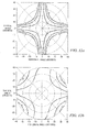
- the excellent performance of this compensator 1110 is clearly shown in FIGURE 12a -b, where field-of-view (FOV) plots are given for uncompensated and compensated perfect homeotropic transmissive panels.
- FOV field-of-view
- transmissive panels will not have reflective symmetry about their cell-center planes, and accordingly a transmissive profile may not exist that would be equivalent to a reflective solution.
- Transmissive pi-cells have a reflection symmetry that can be compensated in this manner.
- LC panels that are almost symmetric about the their cell-center planes are those that have minimal residual in-plane OFF-state retardance.
- An example of this would be a vertically aligned LC mode with very small pre-tilt angle (e.g., ⁇ 2°) away from the substrate normal.
- Another example would be a twisted vertically aligned mode where the net projected in-plane retardance is very small.
- the paired compensators can be brought together on a single side of the panel forming a single compensating element consisting of one or more layers.
- a single layer can be realized by combining equivalent layers such as two equivalent biaxial films.
- compensation schemes can be derived by first unfolding the reflective case assuming perfect homeotropic alignment and second by tilting the compensator in accordance with the tilt of the LC.
- a simple c-plate can be used to compensate a tilted transmissive vertically aligned nematic LC panel by tilting the plate to align the out-of-plane optic axis of the plate to that of the LC.
- the ray deflection at material interfaces should be taken into account making the angle of the plate not match exactly with the LC director.
- Solutions can be derived in the case of compensating finite in-plane residual retardance of a transmissive panel with reflective symmetry such as a pi-cell. Unlike in the reflective case, however, only one solution exists where the input and output polarization are the same. In the case of a tilted, vertically aligned LC system, this would be the matched 45° solution. It is possible, however, to rotate the output analyzer in the transmissive system as the polarizer and analyzer are physically separate. Good contrast can therefore be achieved if the output polarization is linear. This is the same condition as for the solution set determined in Equations 1 and 2. Compensators with in-plane retardances greater than the panels' residuals can therefore be used for in-plane compensation assuming rotation of the output analyzer.
- the analyzer angle for any given solution can be derived using expressions similar to those used in Equation 1.
- field-of-view compensation can then be independently addressed with average retardance values using the equivalence of transmissive to unfolded reflective systems. While the unfolded systems can most easily be applied to systems using crossed a-plates (or other systems not having tilted plates), through design techniques it is possible to develop transmissive systems following many of the reflective architectures described above.
- the compensating stacks described herein may be made from any suitable material such as solid crystals, stretched polymers, liquid crystal polymers, or another material.
- the liquid crystal polymer can have dual homogeneous alignment, splay alignment (homogeneous/homeotropic) or any suitable alignment.
- the compensated retarder stacks are discussed in the context of color management for projection display, they can be used in a number of applications. These include, among others, color separation for image capture or radiometry, lighting, and near infrared optical communications.
Abstract

Description
- Disclosed embodiments herein relate to optical devices for use in liquid crystal (LC) display systems, and more particularly to reflective liquid crystal on silicon (LCoS) projection architectures that require panel-only compensation. These embodiments represent optical components that consist of one or more birefringent layers that compensate for residual in-plane and out-of-plane retardation present in the OFF-state of an LC panel. The net retardation of the panel (= Dn ●d) is then substantially the vector sum of the two retardance components. When reduced to practice with stretched organic polymer films, these components typically demand high durability and high polarization performance, and as such a low-elasticity organic substrate is preferred, as described in the preceding provisional
U.S. Patent Application No. 60/573,910 , which is hereby incorporated by reference herein. - In projection displays using LCOS or other LC panels, there is a need to compensate residual, OFF-state panel retardance to ensure sufficient contrast performance, because such residual in-plane retardance applied to incident optical rays can cause polarization mixing and lead to OFF-state leakage. In the case of large screen televisions based on LC panel projection, this leakage manifests itself as a bright dark-state and one that is often colored. When displaying dark video content, such leakage is very obvious and undesirable. Removing residual OFF-state retardance of the LC panels, or at least its adverse affect, can be achieved by introducing birefringent elements in front of the panel, which was described by U.S. Patent Publication No.
US 2003/0128320, to Xiang-Dong Mi . - In general, compensators act first to remove residual in-plane OFF-state retardance of the panel, and second to reduce OFF-state light leakage due to the out-of-plane retardance which relates to field-of-view (FOV) performance of the LC layer. Removing the in-plane retardance is important, as it affects all incident light, since it corresponds to the extent to which the LC molecules are not aligned normal to the substrate or not balanced in their orientations when projected onto the panel plane. The substantial out-of-plane retardance alters the polarization state of off-axis rays, and acts to reduce the panel's field-of-view and in non-collimated systems leads again to OFF-state leakage. To get the high contrast demanded of current commercial video projection systems, both in-plane and out-of-plane compensation is desired.
-
FIGURES 1a-b are optical block diagram of exemplary compensator and LC panel arrangements, showing for background purposes relative arrangement and orientations of compensators relative to LC panels; -
FIGURE 2 is a graph of optimal compensator optic axis orientation as a function of net in-plane retardance for compensating an exemplary 3 nm residual vertically aligned LCOS panel; -
FIGURE 3 illustrates a first embodiment compensator comprising separate a-plate and c-plate compensators; -
FIGURE 4 illustrates a second embodiment compensator in which a single biaxial compensator is used to compensate for an LC panel; -
FIGURE 5 is a graph illustrating the insensitivity of biaxial out-of-plane retardance for different in-plane compensation values; -
FIGURE 6 illustrates a further embodiment compensator in which a single c-plate is tilted to provide in-plane compensation; -
FIGURE 7 illustrates a bi-layer compensator embodiment for compensating LC reflective panels; -
FIGURE 8 shows the optimum average retardance value for a crossed a-plate compensator as a function of in-plane retardance, again for an exemplary 3 nm residual vertically aligned LCOS panel; -
FIGURE 9 illustrates a compensator constructed in accordance with disclosed manufacturing techniques; -
FIGURE 10 illustrates an unfolded bi-layer compensated transmissive system; -
FIGURE 11 illustrates a transmissive system based on the bi-layer reflective system in which the compensator pairs are placed on one side of the panel and combined into a single compensator; and -
FIGURES 12a-b are exemplary field-of-view diagrams showing respectively the FOV at 550 nm of an uncompensated transmissive homeotropic aligned LC panel and one that is compensated using the approach ofFIGURE 11 . - Certain disclosed compensation schemes may be used in reflective systems where the input/output beam separating PBSs do not require additional compensation (e.g., wire grid PBSs) or are compensated separately. Such systems provide that a linear polarization state exists prior to the system analyzer. Specifically, dark state light exiting the input/output beam-separating PBSs has the same linear polarization state as the light entering as a result of the orthogonal analyzing and polarization axes. In transmissive systems, the output analyzer orientation is independent of the polarizer and allows for compensation solutions that produce rotated linear output states.
- Disclosed herein are embodiments addressing the compensating of a reflective LC panel with a compensator comprising at least one birefringent layer, where each birefringent layer or the collection of birefringent layers can exhibit uniaxial or biaxial properties. Specific cases include a- and c-plate combinations, single biaxial films, tilted c-plates, and bi-layer compensators comprising two uniaxial layers having their optic axes oriented substantially orthogonally with respect to each other. Compensation of transmissive panels can be achieved by related methods and are also covered by the general methodology of this patent by 'unfolding' reflective designs. A stretched organic film may be used as the birefringent layer or layers in the described embodiments. To avoid degradation within the harsh environment of a projection system, compensators using these stretched organic films may be formed as an encapsulated laminate. An exemplary effective organic film is a low-elasticity polyolefin film.
-
FIGURES 1a -b are optical block diagrams illustrating relative layouts and orientations of compensators relative to LC panels (comprising LC layers and reflectors) that they are compensating. In particular,FIGURE 1a shows anoptical system 100 comprising acompensator 102.Polarized light 103 impinges on thecompensator 102, and is shown with a linear (vertical polarization). Thecompensator 102 has a certain optic axis orientation and in-plane retardance, theta r and gamma r, respectively, where theta r is the orientation angle relative to the linear polarization of thepolarized input light 103. Because of the polarization difference, the compensator imparts anelliptical polarization 105 to the light 103 incident on theLC layer 104. The elliptical polarization is configured such that it will compensate for the built-in residual in-plane retardance of theLC layer 104, such that the output from theLC layer 104 will be linearly polarized as it impinges upon thereflection plane 106. Along the reflective path, this process occurs in the reverse order, and thecompensator 102 has been configured such that the output light 103 (along the same path as the input light) has the same linear polarization as the input light. - The
optical system 100 ofFIGURE 1b operates in the same way as theoptical system 100 ofFIGURE 1a , except that inFIGURE 1b thecompensator 102 is positioned between theLC panel 104 and thereflector 106, whereas inFIGURE 1a it was positioned optically ahead of both of those elements. Thecompensator 102 of eitherFIGURE 1a or FIGURE 1b can accordingly be configured to compensate for the elliptical polarization imparted in the OFF-state by theLC panel 104, whether thecompensator 102 is located between theLC panel 104 andreflector 106, as inFIGURE 1b , or optically before both of those elements, as inFIGURE 1a . In practice, placing thecompensator 102 between theLC panel 104 andreflector 106 is seldom done, as usually the LC panel and reflector are packaged as a single component, and may often be described together as a reflective LC panel. It would be possible, however, to arrange the elements as described and shown inFIGURE 1b . Mathematically,FIGURE 1b is also a useful approximation for the more-common architecture ofFIGURE 1a , and that approximation holds particularly for small in-plane panel 104/106 andcompensator 102 retardances. The less conventional arrangement ofFIGURE 1b therefore simplifies the matrix mathematics described below, and accordingly is also described herein. But, as mentioned, the matrix mathematics also accurately describe the more conventional arrangement ofFIGURE 1a for small in-plane panel 104/106 andcompensator 102 retardances. - The above description of
FIGURES 1a-b provides a background for understanding the developments and advancement of the present application, which includes specific approaches in whichLC panels 104 can be compensated by compensating residual OFF-state in-plane retardance together with compensating off-axis polarization mixing caused by the panel's OFF-state out-of-plane retardance. In certain embodiments, this may be viewed as a sequential, two-step process as light passes through the system. But while there may be certain advantages in the order of compensation, and certain statements in the specification may seem to imply a certain order, the use of the described embodiments should not be construed to limit the scope of the claims. The claims alone may require certain orders or sequences of compensation, and as such only those claims specifically spelling out particular orders of compensation should be construed to be so limited. - Still referring to
FIGURE 1A , further described is an embodiment for compensating LC panels. In the embodiment shown, the LC panel includes both anLC material 104 and areflective plane 106. The described embodiment involves first the matching and then negating the in-plane retardance of compensator (gamma r) and panel (gamma p). As described in the present application, exact matching of the retardances is not necessary, and in fact may be undesirable. The system specifically can be configured to compensate for the retardance mismatch between the compensator and the panel by changing the relative orientations between thepanel 104/106 and thecompensators 102. In the described embodiments, the compensation for the retardance mismatch can only be achieved where the compensator's 102 in-plane retardance exceeds the in-plane component of the panel's 104/106 dark-state retardance. - Although the present application describes the
compensators 102 as being positioned outside thepanels 104/106, it is also possible to place the compensators 102 'within'reflective panels 104/106, as is shown inFIGURE 1b . Thus, in theFIGURE 1b embodiment, the compensator is interposed between theLC material 104 and thereflective plane 106. As mentioned above, and as will be further described below, this application recognizes the advantage of having a substantial mismatch between compensator and panel retardances. Certain embodiments of this application accordingly describe approaches or designs that work effectively with the substantial mismatch in compensator and panel retardances. - More specifically, applicants have recognized that from a manufacturing or design stability standpoint, if the in-plane retardance of the compensator 102 (gamma r) and the
panel 104/106 (gamma p) are well-matched, this matching may cause difficulties for maintaining the proper relative orientations. This is due to the sharp changes that can occur in optimal orientations when the retardances of thepanel 104/106 andcompensator 102 are relatively close. As described in the present application, relative orientations of thecompensators 102 and thepanel 104/106 can be adjusted to accommodate for differences between panel and compensator retardances. The relationship between the in-plane retardance mismatch, which is the difference between the panel's OFF-state in-plane residual retardance and the compensator's in-plane retardance, and the resulting optimal compensating orientation can be determined mathematically as is described herein. - With the described approach, polarization analysis is simplified because light having the same linear input and exit polarization states from any reflective birefringent network in an LC-panel-based light modulation system, with the LC-panel in its OFF-state, will have a linear polarization of arbitrary orientation at the reflecting interface. A compensator/panel combination creating linear polarization in a single pass - incident on the mirror/reflecting layer of the reflective LC panel - therefore represents an in-plane compensation solution. In mathematical terms, this condition may be expressed as O = L•C•I , where O and I are the output (mirror) and input linear polarizations and where C and L are the head-on transformations associated with the compensator and LC panel respectively. For small retardances, e.g., less than approximately 30 nm for optical systems handling visible light, these transformations can be reversed to give O = C•L•I .
- Employing a Poincare sphere (see D. Goldstein, Polarized Light, at ch. 12 (2d ed. 2003), which is hereby incorporated by reference herein) as a means of representing and transforming polarizations, the above expression can be written as follows:
-

- In this
Equation 1, as discussed in Goldstein, supra, f and e are the conventional orientation and ellipticity angles describing the polarized state transformed from the input polarization by theLC layer 104. Gamma r and theta r are the in-plane retardance and orientation of thecompensator 102, and lambda is the wavelength of the compensated light. The output polarization is linear if it is orthogonal to the vector (0 0 1), hence the scalar product can be equated to zero inEquation 1. -
Equation 1 can be solved to give the following expression relating compensator orientation as a function of retardance: -

- For the specific case of a vertically aligned LCOS panel, the
LC material 104 of the panel is aligned predominantly homeotropically in its low voltage OFF-state, but has a slight tilt (e.g., 7°) off-normal in the plane bisecting the polarizer/analyzer orientations. For typical LC thickness and birefringence, Equation 3 maps the input polarization state (phi, epsilon) = (0°, 0°) onto the polarization state (0°, 1°), which would be consistent with approximately 3 nm of residual in-plane retardance at an input light wavelength of 550 nm. -
FIGURE 2 illustrates a resulting 'C' curve 202 of optimal compensator orientation (y-axis) as a function of in-plane retardance (x-axis) for theabove Equation 2 when the residual retardance is 3 nm at an input wavelength of 550 nm. For each value of compensator retardance, there are two orientations (theta1, theta2) at which the residual in-plane retardance is compensated, where the orientations are related by theta1= 90° - theta2. Thus for a given gamma r (> gamma p), there are two possible compensator orientations given inFIGURE 2 . In the specific illustration ofFIGURE 2 , the in-plane retardance is shown as an example at gamma r approx. equal 7 nm, which yields theta1 approx. equal 15° and theta2 approx. equal 75°, and given the relatively flat slope of the C-curve 200 in this region, the solution would be relatively impervious to variations in the in-plane retardance values of thecompensator 102 and/orLC panel 104/106. The flatter part of the C-curve exists in some of the described embodiments for gamma r - gamma p > approximately 15 nm. - In cases where chromatic, non-collimated light is compensated, and perhaps in other embodiments, it is beneficial to choose the retarder's in-plane orientation that more closely aligns to the input polarization.
- In further described embodiments of this application, applicants have recognized the advantage in choosing a compensator with an in-plane retardance value gamma r that is mismatched, at least to a certain degree, from that of the panel gamma p in its OFF-state. In particular, because of the steep slope of the C-curve near the 45°
solution 205, where theta approx. equal theta approx. equal 45°, small variations in compensator or panel retardance in the 45° implementation can cause relatively dramatic shifts in the orientation solutions according to the illustrated C-curve ofFIGURE 2 . For example, according to the graph, if in-plane retardance of the compensator shifts from 3 nm to approximately 3.2 nm, a shift in retardance of only approximately 7%, the proper orientation angle shifts approximately a full 10°, from 45° to 55°. Without adjusting the system to compensate for this shift in retardance, there could be a dramatic shift in system performance. - Moving away from the 45°
solution 205 to other portions of the illustrated C-curve 200 provides better systemic tolerance of variations of retardance values, gamma r and gamma p, thereby improving the manufacturability of the optical systems in which the disclosed compensators are employed. An exemplary solution range would be in those solutions on the C-curve where the orientation angle theta is less than approximately 20° and the orientation angle theta is greater than approximately 70° (e.g., in those areas where the C-curve 200 is flattening out). A wider angle range would be where the orientation angle theta1 is less than approximately 30° and the orientation angle theta is greater than approximately 60°. The solutions closer to the 45°solution 205 have the disadvantage of requiring tighter tolerance on the in-plane retardance values in order to maintain the same the optical system components near their optimal orientations. - The above description and specifically
Equation 1 describes solutions whereby the in-plane residual retardance of a panel gamma p can be compensated in a reflective LC projection system by an optical component that has an in-plane retardance gamma r equal to, or greater than, gamma r. Although in-plane compensation only may yield sufficient system performance, a more complete solution requires simultaneous out-of-plane panel compensation. The embodiments of this patent therefore consist of creating a compensating component that has one or more birefringent layers that has an in-plane retardance value greater than that of the panel and properties that can offer some (or indeed complete) out-of-plane compensation. This component can then be oriented in accordance withEquation 1 to ensure good in-plane compensation. -
FIGURE 3 illustrates a system designed to compensate an LC panel's in-plane residual and out-of-plane retardance components. In order to compensate the off-axis rays, and thus improve field-of-view (FOV) performance, the retardance projected onto the plane normal to each ray's propagation direction by the LC layer's out-of-plane retardance must be subtracted. This is conventionally done by introducing negative birefringent plates whose optic axes are normal to the mean optical propagation. These birefringent plates are known as 'c-plates,' and they are set with retardances roughly matching the entire retardance of the panels being compensated (Dn ●d ∼ 250nm). - The approach of
FIGURE 3 illustrates one approach that attacks both in-plane and out-of-plane OFF-state LC panel compensation. This approach comprises a two-layer compensator 300 comprising an in-plane uniaxial compensator (a-plate) 302 complying with the 'head-on' criteria ofEquation 2 and a c-plate 304. Conventional compensator solutions of this general structure are known. But known structures do not appreciate that choosing a relative orientation that is substantially removed from 45° may have surprising advantages. The present application, in contrast, recognizes the advantage of picking theta r to be something other than 45°, and it applies this understanding to the disclosed two-layer compensator 300 ofFIGURE 3 . - According to the approach of
FIGURE 3 , incoming light is precompensated as it passes through thecompensator 300. The a-plate 302 compensates for the OFF-state, in-plane residual retardance of theLC panel 104/106. The c-plate 304 compensates for the off-axis effects of theLC panel 104/106, and specifically will impart a certain retardance on incoming, off-normal light rays to minimize the FOV effects ultimately imparted upon the incoming light by theLC panel 104/106. Theoptical compensator 300 is designed to properly compensate in the composite after light has passed in through thecompensator 300 and as it reflects backs back out after being reflected by the reflecting plane of theLC panel 104/106. -
FIGURE 4 illustrates the combining of the a-plate and c-plate functionality into a single stretchedbiaxial film 400. Using a single stretched biaxial film has also been previously proposed by U.S. Patent Publication No.US 2003/0128320, to Xiang-Dong Mi . However, as described above the present application is the first to recognize the advantage gained by choosing the off-45°, non-matched case for setting the in-plane OFF-state retardance compensation. The proper orientation of thebiaxial film 400 can then be determined in a similar or analogous manner to that set forth above with respect to the a-plate/c-plate compensators. As shown inFIGURE 5 , thebiaxial film 400 exhibits very consistent out-of-plane retardance over a wide range of in-plane retardances, so the film can be effectively oriented to compensate for both in-plane and out-of plane LC panel effects. -
FIGURE 6 illustrates another embodiment, which is a single-layer compensator in which a matched c-plate 600 is tilted along theaxis 602 relative to theLC panel 104/106to create some head-on retardance and oriented according toEquation 2. Under certain circumstances, this provides an efficient and relatively inexpensive approach, although it will not provide the same performance advantages that may be found in other solutions proposed in this application. For example, this approach can be unattractive from an imaging standpoint if the necessary tilt angle is too large, as the tilt can then induce unacceptable astigmatic aberration. -
FIGURE 7 illustrates an approach in which acompensator 700 comprising two orthogonally oriented uniaxial layers ('a-plates') 702, 704 can compensate for both head-on and FOV leakage of theLC panel 104/106. It is known that identical crossed a-plates 702, 704 exhibit c-plate-like properties in planes containing the optic axes of the individual layers. The effective c-plate retardance is equivalent to that of the individual layers. As such, these crosseda-plates LC panel 104/106 in its predominantly homeotropic OFF-state. Since off-normal rays only experience undesired polarization mixing in planes other than those containing the polarizer and analyzer axes, and their worst polarization mixing occurs in those planes bisecting polarization/analyzer axes, orienting crosseda-plates a-plate compensator 700 can effectively compensate the effect of an LC panel's 104/106 out-of-plane retardance. - Applicants have built upon the known use of a crossed
a-plate compensator 700 to compensate the effect of an LC panel's 104/106 out-of-plane retardance and in-plane residual retardance in an efficient and manufacturable way. Specifically, applicants have used novel orientations and retardances of theretarder films - A compound two-
layer compensator 700 made from orthogonally orientedbirefringent layers - Applicants' novel approach involves choosing a certain retardance difference between the compound compensator's in-plane retardance and the panel's OFF-state residual retardance. In an embodiment, the retardance of the
compensator 700 is greater than that of thepanel 104/106. Head-on residual panel retardance is then compensated by orienting the part in accordance withEquation 2. It may further be advantageous to place the optic axis of the film with largest retardance closest to the polarization axis of the incoming light. For compensator angles away from 45°, the out-of-plane compensation favors smaller average retardance values. Further, in the case where a mismatched bi-layer compensator is incorporated into a reflective system, optimal performance is obtained when the layer with largest retardance faces away from the panel. The smaller retardance film is then closest the reflective panel. - As will be further described in
FIGURES 10-11 , related compensation schemes can be derived for transmissive panels. Taking the compensator elements described above for the reflective systems, these elements can be unfolded about the mirror plane of the LC panel and in some cases - particularly if the transmissive LC panel has reflective symmetry about its cell-center plane - an equivalent transmissive system can be formed. -
FIGURE 8 graphically illustrates the optimal average retardance value of two crossed a-plate compensator embodiment for an exemplary 3nm residual, Dn ●d = 250 nm, vertically aligned LCOS panel. An optimal average retardance is obtained as a result of compensating the panel's out-of-plane retardance component. Note that for above 10 nm of in-plane retardance, the average retardance is close to a quarter-wave value. Using this figure and the inventive approaches described in this patent specification, a designer can choose optimal retardance values for acompensator 102. -
FIGURE 9 is a structural drawing of acompensator 900, illustrating a possible construction of the elements described in the present application. Centrally located within the laminate stack forming thecompensator 900 is a dualretarder film laminate 902, where thedual retarder film 902 might be an a-plate and a c-plate or crossed a-plates.Adhesives 904 can be used to attach thedual retarder laminate 902 to glass end-caps 906. Further, anantireflective coating 908 can be applied to the glass end-caps 906. Further details of the described structure is further described in the provisional filing from which this application claims priority and in commonly owned patent application _______, entitled 'High Durability And High Performance Polarization Optics Using a Low-Elasticity Organic Layer,' which is hereby incorporated by reference herein. -
FIGURE 10 illustrates an unfolded transmissive embodiment in which the discussed reflective compensation schemes can be utilized on either side of atransmissive panel 104. Specifically the bi-layer compensator ofFIGURE 7 is shown unfolded, withcompensators transmissive panel 104. This approach works optimally forpanels 104 with reflective symmetry about the cell center. In cases where panels are asymmetric, one or more of thecompensators layers FIGURE 7 , except instead of each compensator layer acting on the light twice (once incoming and once reflected), the light will only pass through each respective layer once. -
FIGURE 11 illustrates an embodiment in which thecompensator 1008 that was at the exit of the unfolded system ofFIGURE 11 is combined with thefront compensator 1002 to form a three-layer compensation element 1100. Note that this approach essentially preserves the order in which the light passes through the previously four layers, but since thelayers FIGURE 10 embodiment, they are lumped together aslayer 1104, which then has two times its normal retardance in theFIGURE 11 embodiment. All of the 3 layers precede thepanel 104 to form thetrilyaer compensator 1100. The excellent performance of this compensator 1110 is clearly shown inFIGURE 12a -b, where field-of-view (FOV) plots are given for uncompensated and compensated perfect homeotropic transmissive panels. - With further reference to the transmissive solutions of
FIGURES 10-11 , in many cases the transmissive panels will not have reflective symmetry about their cell-center planes, and accordingly a transmissive profile may not exist that would be equivalent to a reflective solution. Transmissive pi-cells, however, have a reflection symmetry that can be compensated in this manner. - Other LC panels that are almost symmetric about the their cell-center planes are those that have minimal residual in-plane OFF-state retardance. An example of this would be a vertically aligned LC mode with very small pre-tilt angle (e.g., < 2°) away from the substrate normal. Another example would be a twisted vertically aligned mode where the net projected in-plane retardance is very small.
- In these low residual cases, where the transmissive panel is effectively homeotropic in nature, the paired compensators can be brought together on a single side of the panel forming a single compensating element consisting of one or more layers. A single layer can be realized by combining equivalent layers such as two equivalent biaxial films. In this case we can compensate in a conventional way a low residual effectively homeotropic transmissive LC with a matched biaxial film with very low in-plane retardance (effectively a c-plate).
- Still referring to the transmissive embodiments of
FIGURES 10-11 , it is further possible as another embodiment to use a three-layer orthogonally oriented Dn ●d/2x Dn ●d/ Dn ●d compensator with layer axes bisecting the polarizer and analyzer axes. This is the equivalent of the matched bi-layer compensator above, but applied in a low residual unfolded transmissive system. - For transmissive panels having a significant pretilt, the equivalence to an unfolded LC system is lost. However compensation schemes can be derived by first unfolding the reflective case assuming perfect homeotropic alignment and second by tilting the compensator in accordance with the tilt of the LC. By way of example, a simple c-plate can be used to compensate a tilted transmissive vertically aligned nematic LC panel by tilting the plate to align the out-of-plane optic axis of the plate to that of the LC. In practice, the ray deflection at material interfaces should be taken into account making the angle of the plate not match exactly with the LC director.
- Solutions can be derived in the case of compensating finite in-plane residual retardance of a transmissive panel with reflective symmetry such as a pi-cell. Unlike in the reflective case, however, only one solution exists where the input and output polarization are the same. In the case of a tilted, vertically aligned LC system, this would be the matched 45° solution. It is possible, however, to rotate the output analyzer in the transmissive system as the polarizer and analyzer are physically separate. Good contrast can therefore be achieved if the output polarization is linear. This is the same condition as for the solution set determined in
Equations Equation 1. - As described above, field-of-view compensation can then be independently addressed with average retardance values using the equivalence of transmissive to unfolded reflective systems. While the unfolded systems can most easily be applied to systems using crossed a-plates (or other systems not having tilted plates), through design techniques it is possible to develop transmissive systems following many of the reflective architectures described above.
- The section headings in this application are provided for consistency with the parts of an application suggested under 37 CFR 1.77 or otherwise to provide organizational cues. These headings shall not limit or characterize the invention(s) set out in any patent claims that may issue from this application. Specifically and by way of example, although the headings may refer to a 'Field of the Invention,' the claims should not be limited by the language chosen under this heading to describe the so-called field of the invention. Further, a description of a technology in the 'Background' or 'Description of Related Art' is not be construed as an admission that technology is prior art to the present application. Neither is the 'Summary of the Invention' to be considered as a characterization of the invention(s) set forth in the claims to this application. Further, the reference in these headings to 'Invention' in the singular should not be used to argue that there is a single point of novelty claimed in this application. Multiple inventions may be set forth according to the limitations of the multiple claims associated with this patent specification, and the claims accordingly define the invention(s) that are protected thereby. In all instances, the scope of the claims shall be considered on their merits in light of the specification but should not be constrained by the headings included in this application.
- Realizations in accordance with the present invention have been described in the context of particular embodiments. These embodiments are meant to be illustrative and not limiting. Many variations, modifications, additions, and improvements are possible. Accordingly, plural instances may be provided for components described herein as a single instance. Boundaries between various components and operations are illustrated in the context of specific configurations. Other allocations of functionality are envisioned and will fall within the scope of claims that follow. Structures and functionality presented as discrete components in the exemplary configurations may be implemented as a combined structure or component. These and other variations, modifications, additions, and improvements may fall within the scope of the invention as defined in the claims that follow.
- The compensating stacks described herein may be made from any suitable material such as solid crystals, stretched polymers, liquid crystal polymers, or another material. The liquid crystal polymer can have dual homogeneous alignment, splay alignment (homogeneous/homeotropic) or any suitable alignment. Although the compensated retarder stacks are discussed in the context of color management for projection display, they can be used in a number of applications. These include, among others, color separation for image capture or radiometry, lighting, and near infrared optical communications.
- Although several embodiments of the present invention and its advantages have been described in detail, it should be understood that changes, substitutions, transformations, modifications, variations, permutations and alterations may be made therein without departing from the teachings of the present invention, the spirit and the scope of the invention being set forth by the appended claims.
Claims (12)
- An optical system comprising:an optical component operable to be associated with a reflective LC panel, the optical component comprising one or more birefringent films having, individually or collectively, an in-plane retardance that is substantially greater than the associated LC panel's in-plane OFF-state retardance;the optical component further being positioned in the optical system such that the optical component optimally compensates for the relative retardances between the optical component and the LC panel; andthe optical component further being configured to compensate for out-of-plane retardance of the LC panel's OFF-state.
- An optical system according to claim 1, wherein the orientation of the optical component comprising the one or more birefringent films is chosen according to the formula

where phi and epsilon are the orientation and ellipticity angles describing the polarized state transformed from the input polarization by the LC layer panel, where gamma r and theta r are the in-plane retardance and orientation of the optical component, and where lambda is the wavelength of the compensated light. - An optical system according to claim 3, wherein theta r is chosen to be substantially unequal to 45 degrees.
- An optical system according to claim 1, wherein the optical component comprises:an a-plate having an in-plane retardance that is substantially greater than the in-plane retardance of the LC-panel's OFF-state; anda c-plate that is tilted relative to the a-plate, where the a-plate and c-plate are configured to provide substantially optimal in-plane and out-of-plane compensation for the LC-panel's OFF-state.
- An optical system according to claim 4, wherein the orientation of the optical component comprising the a-plate and the c-plate is chosen according to the formula

where phi and epsilon are the orientation and ellipticity angles describing the polarized state transformed from the input polarization by the LC layer panel, where gamma r and theta r are the in-plane retardance and orientation of the optical component, and where lambda is the wavelength of the compensated light. - An optical system according to claim 5, wherein theta r is chosen to be substantially unequal to 45 degrees.
- An optical system according to claim 1, wherein the optical component comprises:a biaxial retarder film positioned to provide along one axis an in-plane retardation that is substantially greater than the in-plane retardance of the LC-panel's OFF-state, and wherein combined contributions of both axes provide substantially optimal in-plane and out-of-plane compensation for the LC panel.
- An optical system according to claim 7, wherein the orientation of optical component comprising the biaxial retarder film is chosen according to the formula

where phi and epsilon are the orientation and ellipticity angles describing the polarized state transformed from the input polarization by the LC layer panel, where gamma r and theta r are the in-plane retardance and orientation of the optical component, and where lambda is the wavelength of the compensated light. - An optical system according to claim 8, wherein theta r is chosen to be substantially unequal to 45 degrees.
- An optical system according to claim 1, wherein the optical component comprises:a tilted c-plate retarder film positioned to provide a projected component along one axis that provides an in-plane retardation that is substantially greater than the in-plane retardance of the LC-panel's OFF-state, and wherein combined contributions of both projected axes of the tilted c-plate retarder film provide substantially optimal in-plane and out-of-plane compensation of the LC panel.
- An optical system according to claim 10, wherein the orientation of the optical component comprising the tilted c-plate retarder film is chosen according to the formula

where phi and epsilon are the orientation and ellipticity angles describing the polarized state transformed from the input polarization by the LC layer panel, where gamma r and theta r are the in-plane retardance and orientation of the optical component, and where lambda is the wavelength of the compensated light. - An optical system according to claim 11, wherein theta r is chosen to be substantially unequal to 45 degrees.
Applications Claiming Priority (3)
| Application Number | Priority Date | Filing Date | Title |
|---|---|---|---|
| US57391004P | 2004-05-24 | 2004-05-24 | |
| US10/908,671 US7345723B2 (en) | 2004-05-24 | 2005-05-22 | LC panel compensators |
| EP05740439A EP1759237A4 (en) | 2004-05-24 | 2005-05-24 | Lc panel compensators |
Related Parent Applications (1)
| Application Number | Title | Priority Date | Filing Date |
|---|---|---|---|
| EP05740439.4 Division | 2005-05-24 |
Publications (1)
| Publication Number | Publication Date |
|---|---|
| EP2441580A1 true EP2441580A1 (en) | 2012-04-18 |
Family
ID=35424784
Family Applications (2)
| Application Number | Title | Priority Date | Filing Date |
|---|---|---|---|
| EP05740439A Withdrawn EP1759237A4 (en) | 2004-05-24 | 2005-05-24 | Lc panel compensators |
| EP12150510A Ceased EP2441580A1 (en) | 2004-05-24 | 2005-05-24 | LC panel compensators |
Family Applications Before (1)
| Application Number | Title | Priority Date | Filing Date |
|---|---|---|---|
| EP05740439A Withdrawn EP1759237A4 (en) | 2004-05-24 | 2005-05-24 | Lc panel compensators |
Country Status (4)
| Country | Link |
|---|---|
| US (2) | US7345723B2 (en) |
| EP (2) | EP1759237A4 (en) |
| JP (1) | JP4884380B2 (en) |
| WO (1) | WO2005116738A2 (en) |
Families Citing this family (33)
| Publication number | Priority date | Publication date | Assignee | Title |
|---|---|---|---|---|
| US7518662B2 (en) * | 2005-05-22 | 2009-04-14 | Real D | Contrast enhancement for liquid crystal based projection systems |
| US8237876B2 (en) * | 2005-05-25 | 2012-08-07 | Kim Leong Tan | Tilted C-plate retarder compensator and display systems incorporating the same |
| US7671946B2 (en) * | 2005-10-18 | 2010-03-02 | Jds Uniphase Corporation | Electronically compensated LCD assembly |
| US20070200986A1 (en) * | 2005-12-29 | 2007-08-30 | Ong Hiap L | Contrast ratio and viewing angle improvement for a TN- LCD |
| JP4586781B2 (en) * | 2006-09-14 | 2010-11-24 | ソニー株式会社 | Phase difference compensation plate, phase difference compensator, liquid crystal display device and projection type image display device |
| US7898603B2 (en) * | 2006-11-30 | 2011-03-01 | Reald Inc. | Double-shutter lenses with compensators |
| JP4805130B2 (en) * | 2006-12-27 | 2011-11-02 | 富士フイルム株式会社 | Reflective liquid crystal display element and reflective liquid crystal projector |
| EP1980902B1 (en) * | 2007-04-10 | 2015-07-15 | JDS Uniphase Corporation | Twisted nematic xLCD contrast compensation with tilted-plate retarders |
| EP2240814B1 (en) * | 2008-01-22 | 2016-05-04 | Alcatel Lucent | A light modulator for optical image projection |
| USD603445S1 (en) | 2009-03-13 | 2009-11-03 | X6D Limited | 3D glasses |
| USD624952S1 (en) | 2008-10-20 | 2010-10-05 | X6D Ltd. | 3D glasses |
| USD666663S1 (en) | 2008-10-20 | 2012-09-04 | X6D Limited | 3D glasses |
| USRE45394E1 (en) | 2008-10-20 | 2015-03-03 | X6D Limited | 3D glasses |
| US8542326B2 (en) | 2008-11-17 | 2013-09-24 | X6D Limited | 3D shutter glasses for use with LCD displays |
| US20100245999A1 (en) * | 2009-03-30 | 2010-09-30 | Carlow Richard A | Cart For 3D Glasses |
| CA2684513A1 (en) | 2008-11-17 | 2010-05-17 | X6D Limited | Improved performance 3d glasses |
| USD646451S1 (en) | 2009-03-30 | 2011-10-04 | X6D Limited | Cart for 3D glasses |
| USD650956S1 (en) | 2009-05-13 | 2011-12-20 | X6D Limited | Cart for 3D glasses |
| USD672804S1 (en) | 2009-05-13 | 2012-12-18 | X6D Limited | 3D glasses |
| USD671590S1 (en) | 2010-09-10 | 2012-11-27 | X6D Limited | 3D glasses |
| USD669522S1 (en) | 2010-08-27 | 2012-10-23 | X6D Limited | 3D glasses |
| USD692941S1 (en) | 2009-11-16 | 2013-11-05 | X6D Limited | 3D glasses |
| USD662965S1 (en) | 2010-02-04 | 2012-07-03 | X6D Limited | 3D glasses |
| USD664183S1 (en) | 2010-08-27 | 2012-07-24 | X6D Limited | 3D glasses |
| USD711959S1 (en) | 2012-08-10 | 2014-08-26 | X6D Limited | Glasses for amblyopia treatment |
| AU2018230767A1 (en) | 2017-03-08 | 2019-10-03 | Gary Sharp Innovations, Inc. | Wide angle variable neutral density filter |
| WO2019018419A1 (en) | 2017-07-17 | 2019-01-24 | Sharp Gary D | Wide-angle compensation of uniaxial retarder stacks |
| US11249355B2 (en) | 2018-01-29 | 2022-02-15 | Gary Sharp Innovations, Llc | Color switch for reduced color cross-talk |
| EP4254023A3 (en) | 2018-01-29 | 2023-12-06 | Meta Platforms Technologies, LLC | Hollow triple-pass optical elements |
| JP7284182B2 (en) | 2018-03-02 | 2023-05-30 | メタ プラットフォームズ テクノロジーズ, リミテッド ライアビリティ カンパニー | Retarder Stack Pairs for Conversion of Polarization Basis Vectors |
| TWI826607B (en) | 2018-12-07 | 2023-12-21 | 美商思娜公司 | Display system, spatial light modulator system and method of forming display system |
| WO2021021648A1 (en) * | 2019-07-26 | 2021-02-04 | Magic Leap, Inc. | Panel retardance measurement |
| CN112859227A (en) * | 2019-11-28 | 2021-05-28 | 迪睿合株式会社 | Phase difference compensation element, liquid crystal display device, and projection type image display device |
Citations (4)
| Publication number | Priority date | Publication date | Assignee | Title |
|---|---|---|---|---|
| US6271905B1 (en) * | 1998-08-24 | 2001-08-07 | Matsushita Electric Industrial Co., Ltd. | Reflective liquid crystal display device |
| US6587172B1 (en) * | 2000-05-03 | 2003-07-01 | Three-Five Systems, Inc. | Controlled angle retarder with liquid crystal cell bias tuned for a sequence of wavelengths |
| US20030128320A1 (en) | 2002-01-07 | 2003-07-10 | Eastman Kodak Company | Display apparatus using a wire grid polarizing beamsplitter with compensator |
| US20030164909A1 (en) * | 2002-03-01 | 2003-09-04 | Shigeo Shimizu | Reflective liquid crystal projection apparatus |
Family Cites Families (18)
| Publication number | Priority date | Publication date | Assignee | Title |
|---|---|---|---|---|
| US4536063A (en) | 1982-12-14 | 1985-08-20 | Rockwell International Corporation | Transmissive phase retarder |
| US5554673A (en) | 1993-11-29 | 1996-09-10 | Polygenex International, Inc. | Dip molded polyurethane film compositions |
| US6096375A (en) | 1993-12-21 | 2000-08-01 | 3M Innovative Properties Company | Optical polarizer |
| TW397928B (en) | 1993-12-22 | 2000-07-11 | Sumitomo Chemical Co | Process for prodoucing phase retarder film |
| US5822021A (en) | 1996-05-14 | 1998-10-13 | Colorlink, Inc. | Color shutter liquid crystal display system |
| US5751384A (en) | 1995-05-23 | 1998-05-12 | The Board Of Regents Of The University Of Colorado | Color polarizers for polarizing an additive color spectrum along a first axis and it's compliment along a second axis |
| US6417892B1 (en) * | 1995-05-23 | 2002-07-09 | Colorlink, Inc. | Color filters, sequencers and displays using color selective light modulators |
| US6004417A (en) | 1995-12-08 | 1999-12-21 | The Lamson & Sessions Co. | Method for coupling conduits using microencapsulatable solvent adhesive composition |
| US6156433A (en) | 1996-01-26 | 2000-12-05 | Dai Nippon Printing Co., Ltd. | Electrode for plasma display panel and process for producing the same |
| US5888603A (en) | 1996-04-24 | 1999-03-30 | Fergason; James L. | Stacked films birefringent device and method of making same |
| JP3076242B2 (en) * | 1996-04-26 | 2000-08-14 | 株式会社日立製作所 | Liquid crystal display |
| TW412656B (en) * | 1996-04-26 | 2000-11-21 | Hitachi Ltd | Liquid crystal display |
| EP1101213B1 (en) | 1998-07-31 | 2009-05-27 | Colorlink, Inc. | Color filters, sequencers and displays using color selective light modulators |
| US6552767B1 (en) * | 1999-02-15 | 2003-04-22 | Citizen Watch Co., Ltd. | Liquid-crystal display |
| JP3457591B2 (en) * | 1999-10-08 | 2003-10-20 | インターナショナル・ビジネス・マシーンズ・コーポレーション | Liquid crystal display |
| JP2002148623A (en) * | 2000-08-31 | 2002-05-22 | Sharp Corp | Liquid crystal display device |
| US20030103182A1 (en) * | 2001-11-30 | 2003-06-05 | Eastman Kodak Company | Vertically aligned liquid crystal imaging component with compensation layer |
| US7083835B2 (en) * | 2003-07-31 | 2006-08-01 | Eastman Kodak Company | Multilayer optical compensator, liquid crystal display, and process |
-
2005
- 2005-05-22 US US10/908,671 patent/US7345723B2/en active Active
- 2005-05-24 WO PCT/IB2005/051683 patent/WO2005116738A2/en active Application Filing
- 2005-05-24 EP EP05740439A patent/EP1759237A4/en not_active Withdrawn
- 2005-05-24 JP JP2007517574A patent/JP4884380B2/en not_active Expired - Fee Related
- 2005-05-24 EP EP12150510A patent/EP2441580A1/en not_active Ceased
-
2008
- 2008-01-18 US US12/016,875 patent/US7545469B2/en not_active Expired - Fee Related
Patent Citations (4)
| Publication number | Priority date | Publication date | Assignee | Title |
|---|---|---|---|---|
| US6271905B1 (en) * | 1998-08-24 | 2001-08-07 | Matsushita Electric Industrial Co., Ltd. | Reflective liquid crystal display device |
| US6587172B1 (en) * | 2000-05-03 | 2003-07-01 | Three-Five Systems, Inc. | Controlled angle retarder with liquid crystal cell bias tuned for a sequence of wavelengths |
| US20030128320A1 (en) | 2002-01-07 | 2003-07-10 | Eastman Kodak Company | Display apparatus using a wire grid polarizing beamsplitter with compensator |
| US20030164909A1 (en) * | 2002-03-01 | 2003-09-04 | Shigeo Shimizu | Reflective liquid crystal projection apparatus |
Non-Patent Citations (1)
| Title |
|---|
| D. GOLDSTEIN: "Polarized Light(2d ed. )", 2003 |
Also Published As
| Publication number | Publication date |
|---|---|
| WO2005116738A2 (en) | 2005-12-08 |
| US7545469B2 (en) | 2009-06-09 |
| JP2008506974A (en) | 2008-03-06 |
| US20080129939A1 (en) | 2008-06-05 |
| WO2005116738A3 (en) | 2006-06-01 |
| JP4884380B2 (en) | 2012-02-29 |
| US20050264734A1 (en) | 2005-12-01 |
| EP1759237A4 (en) | 2008-09-03 |
| EP1759237A2 (en) | 2007-03-07 |
| US7345723B2 (en) | 2008-03-18 |
Similar Documents
| Publication | Publication Date | Title |
|---|---|---|
| US7345723B2 (en) | LC panel compensators | |
| EP1764644B1 (en) | Optimally oriented trim retarders | |
| CN1869762B (en) | Tilted C-plate retarder compensator and display systems incorporating the same | |
| EP1353214B1 (en) | Optical devices comprising high performance polarizer package | |
| US7170574B2 (en) | Trim retarders incorporating negative birefringence | |
| US6175400B1 (en) | Broadband cholesteric optical device having a broadband cholesteric layer, a positive C-plate and a negative C-plate | |
| WO2020146091A1 (en) | Optical stack for privacy display | |
| WO2019090246A1 (en) | Privacy display apparatus | |
| EP2259131B1 (en) | Liquid crystal display | |
| JP5600379B2 (en) | Single-layer birefringent crystal trim retarder | |
| JP4805130B2 (en) | Reflective liquid crystal display element and reflective liquid crystal projector | |
| EP2009488A1 (en) | Near halfwave retarder for contrast compensation | |
| US20070242228A1 (en) | Compensation schemes for LCoS projection systems using form birefringent polarization beam splitters | |
| EP2053431A2 (en) | Polarization control system and display device | |
| WO2009113208A1 (en) | Liquid crystal display device | |
| JPWO2008078764A1 (en) | Phase difference compensation element, VAN liquid crystal display element, and liquid crystal projector | |
| US11703623B2 (en) | Wide-angle compensation of uniaxial retarder stacks | |
| US8072561B2 (en) | Twisted nematic xLCD contrast compensation with tilted-plate retarders | |
| KR20110105351A (en) | Liquid crystal device and projection display device | |
| US6567142B1 (en) | Reflective liquid crystal display device including a retardation film of two uniaxial films | |
| JP7477609B2 (en) | Phase difference plate, liquid crystal projector, and contrast adjustment method | |
| WO2022004712A1 (en) | Retarder, liquid-crystal projector, and contrast adjustment method | |
| WO2012105428A1 (en) | Liquid crystal display device | |
| Mi et al. | 45.4: Wide Viewing‐Angle Polarizers Having Relaxed Manufacturing Tolerances |
Legal Events
| Date | Code | Title | Description |
|---|---|---|---|
| PUAI | Public reference made under article 153(3) epc to a published international application that has entered the european phase |
Free format text: ORIGINAL CODE: 0009012 |
|
| AC | Divisional application: reference to earlier application |
Ref document number: 1759237 Country of ref document: EP Kind code of ref document: P |
|
| AK | Designated contracting states |
Kind code of ref document: A1 Designated state(s): AT BE BG CH CY CZ DE DK EE ES FI FR GB GR HU IE IS IT LI LT LU MC NL PL PT RO SE SI SK TR |
|
| 17P | Request for examination filed |
Effective date: 20121017 |
|
| 17Q | First examination report despatched |
Effective date: 20140513 |
|
| STAA | Information on the status of an ep patent application or granted ep patent |
Free format text: STATUS: THE APPLICATION HAS BEEN REFUSED |
|
| 18R | Application refused |
Effective date: 20171116 |