WO2012105428A1 - Liquid crystal display device - Google Patents
Liquid crystal display device Download PDFInfo
- Publication number
- WO2012105428A1 WO2012105428A1 PCT/JP2012/051753 JP2012051753W WO2012105428A1 WO 2012105428 A1 WO2012105428 A1 WO 2012105428A1 JP 2012051753 W JP2012051753 W JP 2012051753W WO 2012105428 A1 WO2012105428 A1 WO 2012105428A1
- Authority
- WO
- WIPO (PCT)
- Prior art keywords
- liquid crystal
- display device
- crystal display
- polarizer
- birefringent layer
- Prior art date
Links
Images


Classifications
-
- G—PHYSICS
- G02—OPTICS
- G02B—OPTICAL ELEMENTS, SYSTEMS OR APPARATUS
- G02B5/00—Optical elements other than lenses
- G02B5/30—Polarising elements
- G02B5/3025—Polarisers, i.e. arrangements capable of producing a definite output polarisation state from an unpolarised input state
-
- G—PHYSICS
- G02—OPTICS
- G02F—OPTICAL DEVICES OR ARRANGEMENTS FOR THE CONTROL OF LIGHT BY MODIFICATION OF THE OPTICAL PROPERTIES OF THE MEDIA OF THE ELEMENTS INVOLVED THEREIN; NON-LINEAR OPTICS; FREQUENCY-CHANGING OF LIGHT; OPTICAL LOGIC ELEMENTS; OPTICAL ANALOGUE/DIGITAL CONVERTERS
- G02F1/00—Devices or arrangements for the control of the intensity, colour, phase, polarisation or direction of light arriving from an independent light source, e.g. switching, gating or modulating; Non-linear optics
- G02F1/01—Devices or arrangements for the control of the intensity, colour, phase, polarisation or direction of light arriving from an independent light source, e.g. switching, gating or modulating; Non-linear optics for the control of the intensity, phase, polarisation or colour
- G02F1/13—Devices or arrangements for the control of the intensity, colour, phase, polarisation or direction of light arriving from an independent light source, e.g. switching, gating or modulating; Non-linear optics for the control of the intensity, phase, polarisation or colour based on liquid crystals, e.g. single liquid crystal display cells
- G02F1/133—Constructional arrangements; Operation of liquid crystal cells; Circuit arrangements
- G02F1/1333—Constructional arrangements; Manufacturing methods
- G02F1/1335—Structural association of cells with optical devices, e.g. polarisers or reflectors
- G02F1/13363—Birefringent elements, e.g. for optical compensation
- G02F1/133634—Birefringent elements, e.g. for optical compensation the refractive index Nz perpendicular to the element surface being different from in-plane refractive indices Nx and Ny, e.g. biaxial or with normal optical axis
-
- G—PHYSICS
- G02—OPTICS
- G02F—OPTICAL DEVICES OR ARRANGEMENTS FOR THE CONTROL OF LIGHT BY MODIFICATION OF THE OPTICAL PROPERTIES OF THE MEDIA OF THE ELEMENTS INVOLVED THEREIN; NON-LINEAR OPTICS; FREQUENCY-CHANGING OF LIGHT; OPTICAL LOGIC ELEMENTS; OPTICAL ANALOGUE/DIGITAL CONVERTERS
- G02F2413/00—Indexing scheme related to G02F1/13363, i.e. to birefringent elements, e.g. for optical compensation, characterised by the number, position, orientation or value of the compensation plates
- G02F2413/02—Number of plates being 2
Definitions
- the present invention relates to a liquid crystal display device. More specifically, the present invention relates to a liquid crystal display device including a polarizer and a birefringent layer.
- a liquid crystal display device is usually configured to include an optical element such as a polarizing plate and a retardation film (birefringent layer) together with a liquid crystal panel and a backlight.
- an optical element such as a polarizing plate and a retardation film (birefringent layer) together with a liquid crystal panel and a backlight.
- a liquid crystal layer is sandwiched between upper and lower substrates on the viewer side and the back side, and optical elements for improving optical characteristics are placed on these substrates.
- Such liquid crystal display devices are widely used in electronic devices such as monitors, projectors, cellular phones, and personal digital assistants (PDAs) because of their excellent display characteristics.
- PDAs personal digital assistants
- COA color filter on array
- TFT thin film transistor
- CR contrast ratio
- a dimming backlight that improves the CR (hereinafter also referred to as “dynamic CR”) of a liquid crystal display device by dynamically adjusting the brightness of the backlight brightness according to the brightness of the image is known.
- a liquid crystal display device having a dynamic CR of 10,000 or more is known.
- the CR improvement effect due to the dimming backlight is limited depending on the type of video, or there is room for improvement in that no effect can be obtained.
- the white brightness of the white display is sacrificed and the backlight luminance cannot be reduced.
- This problem is somewhat improved by the local dimming backlight that divides the backlight into multiple blocks whose brightness can be controlled independently, and dimming each block, but the above situation does not change inside the block, so it remains the same. It can be said that the effect is limited.
- the present invention has been made in view of the above situation, and an object of the present invention is to provide a liquid crystal display device capable of suppressing light leakage and improving CR.
- Non-Patent Documents 1 and 2 show that the light leakage observed in the normal direction of the panel due to light scattering is analyzed in detail, and is incident obliquely on the liquid crystal panel. It is shown that the light travels in the normal direction due to the internal scattering of the panel and is not absorbed sufficiently by the polarizer on the observation surface side, resulting in light leakage. This will be described more specifically with reference to FIG. As shown in (1) in FIG. 22, first, obliquely incident light on the liquid crystal panel (liquid crystal cell) 230 is modulated into elliptically polarized light by a retardation film or liquid crystal.
- the traveling direction is changed to the normal direction by scattering (the polarization state hardly changes before and after scattering).
- the polarization state hardly changes before and after scattering.
- the polarization state generally does not change before and after scattering
- the vertical alignment (VA: Vertical Alignment) mode liquid crystal layer and retardation film transmitted after scattering also change the polarization state completely for light traveling in the normal direction. Even if it is not changed or changed, the light leakage at the polarizer on the observation surface side is simply converted to another polarization state where the light leakage is exactly the same.
- Non-Patent Documents 1 and 2 describe the retardation value (
- a color filter that is a main cause of scattering of incident light is provided on the lower substrate side, and the scattering of incident light on the lower substrate is larger than the scattering on the upper substrate.
- the retardation value of the retardation film is adjusted to be small, a sufficient CR improvement effect cannot be obtained. This is because the polarization state changes greatly before and after passing through the VA liquid crystal layer even if it is in a polarization state in which light does not leak even if it is scattered in the normal direction when the lower substrate is incident due to the polarizer.
- Non-Patent Documents 1 and 2 When the present inventors scrutinized the liquid crystal display devices (liquid crystal panels) described in Non-Patent Documents 1 and 2 above, CR was improved compared to the conventional configuration using a retardation film having a large retardation value on the lower side. However, leakage of light incident from an oblique direction and scattered in the normal direction is not sufficiently suppressed, and there is room for improvement in that light leakage occurs from the polarizer on the observation surface side. It has been found.
- the inventors of the present invention have made further studies and found that the polarization state of the incident light from the oblique direction is different from the polarization state corresponding to the extinction position when the polarizer on the observation surface side is viewed from the normal direction. Accordingly, it has been found that light incident from an oblique direction and scattered in the normal direction of the polarizer on the observation surface side is emitted as light leakage.
- one embodiment of the present invention is a liquid crystal display device including a first polarizer, one or more first birefringent layers (retardation film), a liquid crystal cell, and a second polarizer in this order from the back side.
- the liquid crystal cell includes a pair of opposing substrates (a lower substrate and an upper substrate) and a liquid crystal layer sandwiched between the substrates, and the absorption axis of the first polarizer is the second polarization
- the liquid crystal display device includes two or more first birefringent layers substantially orthogonal to the absorption axis of the child, the two or more first birefringent layers have at least one of an NZ coefficient and a phase difference.
- a plurality of different birefringent layers are included, and the one or more first birefringent layers pass through the first polarizer, and the polarization state of light incident from an oblique direction is determined by the method of the second polarizer.
- a liquid crystal display device (hereinafter referred to as “the present invention”) that converts the polarization state to the extinction level when viewed from the line direction.
- the “light incident from an oblique direction” specifically refers to an azimuth range of 45 ° ⁇ 22.5 ° and an azimuth direction 135 when the absorption axis direction of the first polarizer is defined as azimuths of 0 ° and 180 °.
- the light is incident from the range of ⁇ 22.5 ° and the direction of 225 ° ⁇ 22.5 ° or the range of 315 ° ⁇ 22.5 °.
- “converting the polarization state of incident light into an extinction level when viewed from the normal direction of the second polarizer” means, in other words, converting the polarization state of incident light (polarized light) into linearly polarized light ( It can be said that the vibration direction is substantially matched with the absorption axis direction of the second polarizer.
- “substantially coincide” refers to a state where the distance between two points on a Poincare sphere having a radius of 1 is 0.15 or less.
- the polarization state of the light converted by the first birefringent layer may be elliptical polarization instead of perfect linear polarization.
- the configuration of the first liquid crystal display device of the present invention is not particularly limited by other components as long as such components are essential.
- the type (NZ coefficient), number, retardation value, material, and the like of the first birefringent layer can be appropriately selected.
- the first birefringent layer May be a form consisting of only a single (one) birefringent layer, or may be a form consisting of only a plurality of birefringent layers having different NZ coefficients and phase differences from each other.
- a form more specifically, including a plurality of birefringent layers having the same NZ coefficient and retardation, and at least one birefringent layer having at least one of the NZ coefficient and the phase difference different from the plurality of birefringent layers.
- a liquid crystal display device including such a birefringent layer is also an embodiment of the present invention. That is, another aspect of the present invention is a liquid crystal display device including a first polarizer, a first first-type birefringent layer, a liquid crystal cell (liquid crystal panel), and a second polarizer in this order from the back side.
- the liquid crystal cell includes a pair of opposing substrates (a lower substrate and an upper substrate) and a liquid crystal layer sandwiched between the substrates, and an in-plane retardation of the first first-type birefringent layer.
- the phase axis is substantially parallel to the absorption axis of the second polarizer
- the absorption axis of the first polarizer is substantially orthogonal to the absorption axis of the second polarizer
- the first first When a NZ coefficient of a birefringent layer is NZ11 and an in-plane retardation is R11, a liquid crystal display device satisfying the following formulas (2-1) and (2-2) (hereinafter referred to as “second embodiment of the present invention”). It is also referred to as a “liquid crystal display device”.
- the manufacturing process can be simplified and the thickness can be reduced as compared with the case where a plurality of types of birefringent layers are combined.
- each birefringent layer can be manufactured easily.
- the configuration of the second liquid crystal display device of the present invention is not particularly limited by other components as long as such components are essential.
- Still another embodiment of the present invention is a liquid crystal display device having a first polarizer, a first first-type birefringent layer, a liquid crystal cell (liquid crystal panel), and a second polarizer in this order from the back side.
- the liquid crystal cell includes a pair of opposing substrates (a lower substrate and an upper substrate) and a liquid crystal layer sandwiched between both substrates, and the in-plane of the first type birefringent layer.
- the slow axis is substantially perpendicular to the absorption axis of the second polarizer
- the absorption axis of the first polarizer is substantially perpendicular to the absorption axis of the second polarizer
- the first first When a NZ coefficient of a birefringent layer is NZ11 and an in-plane retardation is R11, a liquid crystal display device satisfying the following formulas (3-1) and (3-2) (hereinafter referred to as “third embodiment of the present invention”). It is also referred to as a “liquid crystal display device”.
- the third liquid crystal display device of the present invention is also observed even when light obliquely incident on the lower substrate changes its traveling direction in the normal direction due to scattering. It is sufficiently absorbed by the surface-side polarizer, and a large CR improvement effect is obtained.
- the manufacturing process can be simplified and the thickness can be reduced as compared with the case where a plurality of types of birefringent layers are combined.
- the configuration of the third liquid crystal display device of the present invention is not particularly limited by other components as long as such components are formed as essential.
- the first liquid crystal display device of the present invention further includes one or two or more second birefringent layers between the liquid crystal cell and the second polarizer, and the liquid crystal display device has two or more second birefringent layers.
- the two or more second birefringent layers include a plurality of birefringent layers having different NZ coefficients and retardations, the liquid crystal layer, and the one or more birefringent layers.
- the second birefringent layer preferably does not substantially change the polarization state of light incident from the normal direction during black display. As a result, even if the light converted into the polarization state of the extinction position of the second polarizer is scattered in the normal direction inside the liquid crystal display device, it can be absorbed by the second polarizer. The improvement effect can be enhanced.
- the type (NZ coefficient), number, retardation value, material, and the like of the second birefringent layer can be appropriately selected.
- the second birefringent layer May be a form consisting of only a single (one) birefringent layer, or may be a form consisting of only a plurality of birefringent layers having different NZ coefficients and phase differences from each other.
- a form more specifically, including a plurality of birefringent layers having the same NZ coefficient and retardation, and at least one birefringent layer having at least one of the NZ coefficient and the phase difference different from the plurality of birefringent layers.
- a form including two identical positive C plates and one positive A plate May be, for example, a form including two identical positive C plates and one positive A plate).
- a form including a first birefringent layer, a form including a second birefringent layer and a fourth birefringent layer, a form including a third birefringent layer and a fifth birefringent layer Is preferred.
- the second liquid crystal display device of the present invention it is preferable that 0.15 ⁇ NZ11 ⁇ 0.35 and 250 nm ⁇ R11 ⁇ 290 nm are satisfied. As a result, even if light obliquely incident on the lower substrate changes its traveling direction in the normal direction due to scattering, it is sufficiently absorbed by the polarizer on the observation surface side, and a greater CR improvement effect is obtained.
- the second liquid crystal display device of the present invention further includes a second type of birefringent layer and a second type of birefringent layer between the liquid crystal cell and the second polarizer.
- the liquid crystal molecules in the liquid crystal layer are substantially vertically aligned during black display, and the in-plane slow axis of the second first-type birefringent layer is the absorption of the second polarizer.
- the NZ coefficient of the second type birefringent layer is NZ12
- the in-plane retardation is R12
- the thickness direction retardation of the second type birefringent layer is Rth2
- black When the thickness direction retardation of the liquid crystal cell at the time of display is Rthlc, a form satisfying the following formulas (2-3) to (2-5) (hereinafter also referred to as “first form”) is preferable.
- first form a form satisfying the following formulas (2-3) to (2-5) (hereinafter also referred to as “first form”) is preferable.
- 0.65 ⁇ NZ12 ⁇ 0.85 and 250 nm ⁇ R12 ⁇ 290 nm are preferably satisfied, and ⁇ 30 nm ⁇ Rth2 + Rthlc ⁇ 30 nm is preferably satisfied.
- the NZ coefficient of the second birefringent layer is NZ2, it is preferable that 5 ⁇ NZ2 is satisfied in the first embodiment, and it is more preferable that 10 ⁇ NZ2 is satisfied. Thereby, the light leakage from the oblique direction can be further reduced and the viewing angle can be expanded.
- the third liquid crystal display device of the present invention it is preferable that 0.65 ⁇ NZ11 ⁇ 0.85 and 250 nm ⁇ R11 ⁇ 290 nm are satisfied. As a result, even if light obliquely incident on the lower substrate changes its traveling direction in the normal direction due to scattering, it is sufficiently absorbed by the polarizer on the observation surface side, and a greater CR improvement effect is obtained.
- the third liquid crystal display device of the present invention further includes a second birefringent layer and a second first birefringent layer between the liquid crystal cell and the second polarizer.
- the liquid crystal molecules in the liquid crystal layer are substantially vertically aligned during black display, and the in-plane slow axis of the second first-type birefringent layer is the absorption of the second polarizer.
- the NZ coefficient of the second birefringent layer of the second type is NZ12
- the in-plane retardation is R12
- the thickness direction retardation of the second birefringent layer is Rth2
- black display When the thickness direction retardation of the liquid crystal cell at this time is Rthlc, a form satisfying the following formulas (3-3) to (3-5) (hereinafter also referred to as “second form”) is preferable.
- 0.15 ⁇ NZ12 ⁇ 0.35 and 250 nm ⁇ R12 ⁇ 290 nm are preferably satisfied, and ⁇ 30 nm ⁇ Rth2 + Rthlc ⁇ 30 nm is preferably satisfied.
- the NZ coefficient of the second birefringent layer is NZ2
- 5 ⁇ NZ2 is preferably satisfied
- 10 ⁇ NZ2 is more preferably satisfied.
- the upper A form in which the scattering of the substrate is smaller than that of the lower substrate (hereinafter, also referred to as “third form”) is preferable.
- the size of the scattering of the upper and lower substrates is determined by measuring the transmittance by sandwiching both of them between the same crossed Nicol polarizing plate and the parallel Nicol polarizing plate, and calculating the contrast. The higher one is discriminated as a substrate with less scattering.
- the lower substrate preferably includes a color filter (CF) layer and a thin film transistor (TFT), and the liquid crystal cell preferably has a color filter on array (COA) structure.
- the liquid crystal cell preferably includes a dye-based color filter layer, and the liquid crystal cell preferably does not include a color filter layer.
- the TFT here means not only the TFT (transistor) itself but also a broad TFT including other materials and structures generally provided in the TFT substrate.
- a pigment-based CF layer is generally used as the CF layer, and both the pigment-based CF layer and the TFT can be a major factor in the scattering of incident light.
- the scattering of the upper substrate can be made smaller than that of the lower substrate.
- the wirings exposed to the openings particularly affect scattering.
- wiring extending in an orientation that is neither parallel nor orthogonal to the absorption axis or transmission axis of the polarizer causes scattering (may be diffraction).
- the edge portion of the Cs wiring appears to shine due to scattering or diffraction.
- the quality of the organic insulating film the presence or absence of surface irregularities
- the scattering of the upper substrate is brought close to zero by making the CF layer a dye-based CF layer that has very little scattering.
- the scattering of the upper substrate can be made smaller than that of the lower substrate. Further, by providing the TFT on the lower substrate without providing the CF layer, the scattering of the upper substrate can be made close to zero and the scattering of the upper substrate can be made smaller than that of the lower substrate.
- the substrate including the CF layer may include a member such as a BM (black matrix) layer, an alignment film, and a transparent electrode (ITO), but scattering due to these is negligibly small compared to that of the pigment-based CF layer. .
- the first, second and third liquid crystal display devices of the present invention light leakage can be suppressed and CR can be improved.
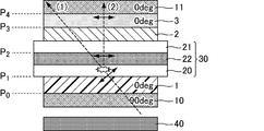
- FIG. 1 is a schematic cross-sectional view of a liquid crystal display device according to Embodiment 1.
- FIG. FIG. 3 is a schematic cross-sectional view illustrating a state of light incident from an oblique direction in the liquid crystal display device according to the first embodiment.
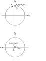
- the liquid crystal display device which concerns on Embodiment 1 it is a figure which shows the transition of a polarization state on the Poincare sphere when the light incident from an oblique direction is not scattered.
- the transition of the polarization state when light incident from an oblique direction is scattered in the direction perpendicular to the observation surface by the lower substrate is shown on the Poincare sphere.
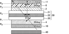
- FIG. 6 is a schematic cross-sectional view of a liquid crystal display device according to Embodiment 2.
- FIG. In the liquid crystal display device which concerns on Embodiment 2, it is a cross-sectional schematic diagram which shows the mode of the light incident from the diagonal direction.
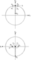
- the liquid crystal display device which concerns on Embodiment 2 it is a figure which shows the transition of a polarization state when the light which enters from an oblique direction is not scattered on a Poincare sphere.
- it is a figure which shows the transition of a polarization state on the Poincare sphere when the light which injected from an oblique direction is scattered in a perpendicular direction with respect to an observation surface by the lower board
- FIG. 6 is a schematic cross-sectional view of a liquid crystal display device according to Embodiment 3.
- FIG. In the liquid crystal display device which concerns on Embodiment 3, it is a cross-sectional schematic diagram which shows the mode of the light which injects from the diagonal direction. In the liquid crystal display device which concerns on Embodiment 3, it is a figure which shows the transition of a polarization state when the light which enters from an oblique direction is not scattered on a Poincare sphere.
- the liquid crystal display device which concerns on Embodiment 3 it is a figure which shows the transition of a polarization state on the Poincare sphere when the light which injected from an oblique direction is scattered in a perpendicular
- the liquid crystal display device which concerns on the comparative form 1 it is a cross-sectional schematic diagram which shows the mode of the light which injected from the diagonal direction.
- liquid crystal display device which concerns on the comparative form 1 it is a figure which shows the transition of a polarization state on the Poincare sphere when the light which injected from an oblique direction is scattered in a perpendicular direction with respect to an observation surface by a lower board
- the liquid crystal display device which concerns on the comparison form 2 it is a cross-sectional schematic diagram which shows the mode of the light which injects from the diagonal direction.
- liquid crystal display device which concerns on the comparative form 2 it is a figure which shows the transition of a polarization state on the Poincare sphere when the light which injected from an oblique direction is scattered in a perpendicular
- liquid crystal display device which concerns on the comparative form 3 it is a cross-sectional schematic diagram which shows the mode of the light which injected from the diagonal direction.
- a polarizer has a function of extracting polarized light (linearly polarized light) that vibrates only in a specific direction from non-polarized light (natural light), partially polarized light, or polarized light.
- polarizer in this specification refers to only a device having a polarizing function without including a protective film.
- ns is the larger of nx and ny, and the nf is the smaller of nx and ny.
- nx and ny indicate the main refractive index in the in-plane direction of the birefringent layer (also applicable to a liquid crystal panel), and nz is the main refractive index in the out-of-plane direction, that is, in the direction perpendicular to the surface of the birefringent layer.
- D represents the thickness of the birefringent layer.
- the measurement wavelength of optical parameters such as the main refractive index, phase difference, and NZ coefficient is 550 nm unless otherwise specified.
- a birefringent layer is a layer (film) having optical anisotropy.
- the birefringent layer means that one of the in-plane retardation R and the absolute value of the thickness direction retardation Rth has a value of 10 nm or more, and preferably has a value of 20 nm or more. .
- the axis angle means the absorption axis of a polarizer or the slow axis of a birefringent layer unless otherwise specified.
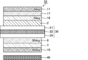
- the liquid crystal display device 50 of the present embodiment is a transmissive liquid crystal display device, and as shown in FIG. 1, in order from the back side, a backlight (BL) unit 40, a first polarizer 10, and a first type of composite device.
- BL backlight
- first polarizer 10 first type of composite device.
- This embodiment is an embodiment according to the first and second liquid crystal display devices of the present invention.
- the material of the birefringent layer used in Embodiment 1 is not particularly limited.
- a stretched polymer film, a fixed liquid crystal material orientation, a thin plate made of an inorganic material, or the like can be used.
- the method for forming the birefringent layer is not particularly limited. In the case of a birefringent layer formed from a polymer film, for example, a solvent casting method, a melt extrusion method, or the like can be used. A method of simultaneously forming a plurality of birefringent layers by a coextrusion method may be used.
- the film may be unstretched or may be stretched.
- the stretching method is not particularly limited, and stretching is performed under the action of the shrinkage force of the heat-shrinkable film, in addition to the inter-roll tensile stretching method, the inter-roll compression stretching method, the tenter transverse uniaxial stretching method, the oblique stretching method, the longitudinal and transverse biaxial stretching method.
- a special stretching method or the like can be used.
- a birefringent layer formed of a liquid crystalline material for example, a method of applying a liquid crystalline material on an orientation-treated base film and fixing the orientation can be used.
- a method of not performing a special orientation treatment on the base film a method of removing the base film from the base film and transferring it to another film may be used. . Further, a method that does not fix the alignment of the liquid crystal material may be used.
- a birefringent layer formed from a non-liquid crystalline material the same formation method as that for a birefringent layer formed from a liquid crystalline material may be used.
- more specific description will be given for each type of birefringent layer.
- a birefringent layer (retardation film) of 0 ⁇ NZ ⁇ 1 is referred to as a first type birefringent layer.
- a film obtained by stretching a film containing a material having a positive or negative intrinsic birefringence as a component under the action of the shrinkage force of a heat-shrinkable film can be appropriately used.
- Japanese Patent No. 2818983 discloses a method for producing a birefringent layer that is stretched under the action of the shrinkage force of the heat-shrinkable film.
- a birefringent layer (retardation film) of NZ >> 1 or a so-called negative C plate is referred to as a second type birefringent layer.
- a film containing a material having a positive intrinsic birefringence as a component is subjected to longitudinal and transverse biaxial stretching processing, or a liquid crystal material such as cholesteric (chiral nematic) liquid crystal or discotic liquid crystal is applied.
- a material coated with a non-liquid crystalline material containing polyimide, polyamide, or the like can be used as appropriate.
- a birefringent layer (retardation film) of NZ ⁇ 1 is referred to as a third type birefringent layer.
- a film obtained by stretching a film containing a material having a positive intrinsic birefringence as a component can be appropriately used.
- the material having a positive intrinsic birefringence include polycarbonate, polysulfone, polyethersulfone, polyethylene terephthalate, polyethylene, polyvinyl alcohol, norbornene, triacetylcellulose, and diacylcellulose.
- a birefringent layer (retardation film) of NZ ⁇ 0 is referred to as a fourth type birefringent layer.
- the fourth kind of birefringent layer is a stretched film containing a material having a negative intrinsic birefringence as a component, and a film containing a material having a positive intrinsic birefringence as a component is acting on the shrinkage force of the heat shrinkable film What extended
- stretched and processed below can be used suitably.
- a film obtained by stretching a film containing a material having a negative intrinsic birefringence as a component is preferable.
- Examples of the material having a negative intrinsic birefringence include a resin composition containing an acrylic resin and a styrene resin, polystyrene, polyvinyl naphthalene, polyvinyl biphenyl, polyvinyl pyridine, polymethyl methacrylate, polymethyl acrylate, and an N-substituted maleimide copolymer. , Polycarbonate having a fluorene skeleton, and triacetyl cellulose (particularly those having a low degree of acetylation). Among these, from the viewpoint of optical properties, productivity, and heat resistance, a resin composition containing an acrylic resin and a styrene resin is preferable. A method for producing a film containing such a resin composition as a component is disclosed in, for example, JP-A-2008-146003.
- a birefringent layer (retardation film) of NZ ⁇ 0, a so-called positive C plate is referred to as a fourth type birefringent layer.
- a film containing a material having a negative intrinsic birefringence as a component and subjected to longitudinal and lateral biaxial stretching processing, a film coated with a liquid crystalline material such as a rod-like nematic liquid crystal, and the like can be used as appropriate. .
- the polarizer used in Embodiment 1 is not particularly limited with respect to materials and optical performance. Specifically, a polarizer or the like in which an anisotropic material such as an iodine complex having dichroism is adsorbed and oriented on a polyvinyl alcohol (PVA) film can be appropriately used.
- PVA polyvinyl alcohol
- a protective film such as a triacetyl cellulose (TAC) film may be laminated on both sides of the polarizer.
- TAC triacetyl cellulose
- the protective film is attached to the polarizer via any suitable adhesive layer (not shown).
- the birefringent layer may have the function of a protective film.
- the “adhesive layer” refers to a layer that joins surfaces of adjacent optical members and integrates them with practically sufficient adhesive force and adhesion time.
- the material for forming the adhesive layer include an adhesive and an anchor coat agent.
- the adhesive layer may have a multilayer structure in which an anchor coat layer is formed on the surface of an adherend and an adhesive layer is formed thereon. Further, it may be a thin layer that cannot be visually recognized.
- the liquid crystal cell only needs to perform black display by aligning liquid crystal molecules in the liquid crystal layer substantially perpendicularly to the substrate surface, and may perform black display when a voltage is applied. It is also possible to perform black display when adding.
- the polarizers 10 and 11 are arranged in crossed Nicols, the liquid crystal display device of the present embodiment is driven in a normally white mode when black display is performed when a voltage is applied, and no voltage is applied. When black display is sometimes performed, it is driven in a normally black mode.
- a display mode of a liquid crystal cell that performs black display when no voltage is applied for example, a VA mode is exemplified.
- the liquid crystal cell may be driven by a simple matrix method (passive matrix method), a plasma address method, or the like.
- a simple matrix method passive matrix method
- a plasma address method or the like.
- a liquid crystal cell for example, a liquid crystal layer is sandwiched between a pair of substrates on which electrodes are formed, and display is performed by applying a voltage between the electrodes.
- VA mode examples include an MVA (Multi-domain Vertical Alignment) mode, a CPA (Continuous Pinwheel Alignment) mode, a PVA (Patterned Vertical Alignment) mode, a BVA (Biased Vertical Alignment) mode, and an RTN (Reverse Twisted Nematic) mode.
- UV2A Ultra Violet Induced VA
- PSA Polymer Sustained Alignment
- IPS-VA In Plane Switching-Vertical Alignment
- TBA Transverese Bend Alignment
- the average pretilt angle of the liquid crystal molecules is preferably 80 ° or more (more preferably 85 ° or more).
- a display mode of a liquid crystal cell that performs black display when a voltage is applied for example, a TN (TwistedwNematic) mode can be given.
- the scattering of the upper substrate is more than the scattering of the lower substrate (non-observation surface side substrate).
- a small liquid crystal panel is more preferable.
- a liquid crystal panel having a color filter on array (COA) structure in which a CF layer is provided on a lower substrate together with a TFT is more preferable. Both the CF layer and the TFT cause large scattering of incident light. However, since these are concentrated on the lower substrate, the scattering of the upper substrate can be surely made smaller than the scattering of the lower substrate.
- COA color filter on array
- liquid crystal panel having the COA structure examples include a liquid crystal panel mounted on a Samsung liquid crystal television (trade name: UN46C7000).
- liquid crystal panels using a dye-based CF layer which is considered to have little scattering
- black and white panels that do not include a CF layer can make the scattering of the upper substrate close to zero and smaller than the scattering of the lower substrate. Can be preferably used.
- the backlight (BL) unit is not particularly limited.
- a light source including at least a light source such as can be used as appropriate.
- the BL unit itself includes an optical sheet such as a lens sheet or prism sheet, and has a collimating function. It may be.
- the first polarizer 10 and the second polarizer 11 are arranged so that their absorption axes are substantially orthogonal to each other.
- the term “substantially orthogonal” specifically means that the angle formed by the absorption axes of each other is within a range of 90 ⁇ 3 ° (preferably 90 ⁇ 1 °, more preferably 90 ⁇ 0.5 °). That means.
- the first type birefringent layer 1 is arranged so that the in-plane slow axis is substantially parallel to the absorption axis of the second polarizer 11, and the first type birefringent layer 3 is an in-plane slow phase.
- the axis is arranged so as to be substantially parallel to the absorption axis of the second polarizer 11.
- substantially parallel means that in any case, specifically, the angle formed by the in-plane slow layer axis and the absorption axis is 0 ⁇ 3 ° (preferably 0 ⁇ 1 °, more preferably 0 ⁇ 0.5 °).
- the NZ coefficient NZ11 of the first type birefringent layer 1 satisfies 0 ⁇ NZ11 ⁇ 0.5, and the in-plane retardation R11 of the first type birefringent layer 1 satisfies 220 nm ⁇ R11 ⁇ 320 nm.
- the NZ coefficient NZ12 of the first type birefringent layer 3 satisfies 0.5 ⁇ NZ12 ⁇ 1.0, and the in-plane retardation R12 of the first type birefringent layer 3 satisfies 220 nm ⁇ R12 ⁇ 320 nm. Fulfill.
- the sum of the thickness direction retardation Rth2 of the second birefringent layer 2 and the thickness direction retardation Rthlc of the liquid crystal cell 30 during black display satisfies ⁇ 50 nm ⁇ Rth2 + Rthlc ⁇ 50 nm.
- liquid crystal display device 50 of the first embodiment light obliquely incident on the substrate 20 is absorbed by the second polarizer 11 even if the traveling direction is changed to the normal direction due to scattering, and thus light leakage is suppressed. A large CR improvement effect is obtained.
- light that is obliquely incident on the substrate 20 and is transmitted through the liquid crystal cell 30 without being scattered is also absorbed by the second polarizer 11, thereby reducing light leakage from the oblique direction.
- the viewing angle can be enlarged.
- FIG. 2 is a schematic cross-sectional view showing a state in which light is incident on the liquid crystal display device of the first embodiment (no voltage applied, black display state) from an oblique direction of 45 ° polar angle and 60 °.
- the light is shown. Since the second birefringent layer 2 and the VA liquid crystal layer have no in-plane anisotropy, the axis angle is not shown in FIG.
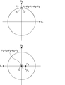
- Poincare sphere The concept of Poincare sphere is widely known in the field of crystal optics and the like as a useful technique for tracking the polarization state changing through the birefringent layer (for example, Hiroshi Takasaki, “Crystal optics”, Morikita Publishing, 1975, p.146-163).
- right-handed polarized light is represented in the upper hemisphere
- left-handed polarized light is represented in the lower hemisphere
- linearly polarized light is represented in the equator
- right circularly polarized light and left circularly polarized light are represented in the upper and lower poles.
- the two polarization states that are symmetric with respect to the center of the sphere form a pair of orthogonal polarization because the absolute values of the ellipticity angles are equal and the polarities are opposite.
- the effect of the birefringent layer on the Poincare sphere is that the polarization state immediately before passing through the birefringent layer is expressed by the slow axis on the Poincare sphere (more precisely, the natural vibration of two birefringent layers).
- the change in the polarization state of the light of (1) above is the polarization state each time the light emitted from the backlight unit 40 passes through the first polarizer 10, each birefringent layer, and the liquid crystal layer 22 (VA liquid crystal layer).
- Point E is a point representing the polarization state of the extinction position (polarized light oscillating in the absorption axis direction) of the second polarizer 11 when viewed from an oblique direction of 45 ° azimuth and 60 ° polar angle.
- a point P0 representing the polarization state of the light after passing through the first polarizer 10 passes through the first-type birefringent layer 1 to P1, passes through the liquid crystal layer 22 to P2, and second-type birefringence. By passing through the layer 2, it is converted to P3, and by passing through the first kind birefringent layer 3, it is converted to P4.
- the polar angle is 45 °.
- Light incident from an oblique direction of 60 ° is finally absorbed by the second polarizer 11. That is, the original function of the retardation film, which reduces the light leakage from the oblique direction and expands the viewing angle, is working normally.
- the point P0 representing the polarization state of the light after passing through the first polarizer 10 is converted to P1 by passing through the first type birefringent layer 1, and then scattered by the lower substrate 20, whereby the law Although the traveling direction is changed to the linear direction, it may be considered that the polarization state hardly changes before and after the scattering (see, for example, Non-Patent Document 2), so even after the scattering progresses in the normal direction.
- Points P2 and P3 representing the polarization state after passing through do not change from P1.
- P3 undergoes rotational movement around the slow axis on the Poincare sphere of the retardation film 3, but the slow axis of the retardation film 3 is Poincare sphere.
- the liquid crystal display device 51 of the present embodiment is a transmissive liquid crystal display device, and as shown in FIG. 5, in order from the back side, a backlight (BL) unit 40, a first polarizer 10, and a first type of composite device.
- a refraction layer 4 (corresponding to the first first birefringent layer), a liquid crystal cell 30 including a liquid crystal layer 22 sandwiched between the substrates 20 and 21, a second birefringent layer 2, a first birefringent layer.
- This is a liquid crystal display device obtained by laminating the refractive layer 6 (corresponding to the above-mentioned second type birefringent layer) and the second polarizer 11 in this order.
- the present embodiment is the same as the first embodiment. Therefore, in the following, items different from the first embodiment will be mainly described.
- This embodiment is an embodiment according to the first and third liquid crystal display devices of the present invention.
- the NZ coefficient NZ11 of the first type birefringent layer 4 satisfies 0.5 ⁇ NZ11 ⁇ 1.0, and the in-plane retardation R11 of the first type birefringent layer 4 satisfies 220 nm ⁇ R11 ⁇ 320 nm.
- the NZ coefficient NZ12 of the first type birefringent layer 6 satisfies 0 ⁇ NZ12 ⁇ 0.5, and the in-plane retardation R12 of the first type birefringent layer 6 satisfies 220 nm ⁇ R12 ⁇ 320 nm.
- the first type birefringent layer 4 is disposed so that the in-plane slow axis is substantially parallel to the absorption axis of the second polarizer 11, and the first type birefringent layer 6 is provided with an in-plane slow phase.
- the axis is arranged so as to be substantially parallel to the absorption axis of the second polarizer 11.
- substantially parallel means that in any case, specifically, the angle formed by the in-plane slow layer axis and the absorption axis is 0 ⁇ 3 ° (preferably 0 ⁇ 1 °, more preferably 0 ⁇ 0.5 °).
- liquid crystal display device 51 of the second embodiment According to the liquid crystal display device 51 of the second embodiment, light obliquely incident on the substrate 20 is absorbed by the second polarizer 11 even if the traveling direction is changed to the normal direction due to scattering, and thus light leakage is suppressed. A large CR improvement effect is obtained. In addition, light that is obliquely incident on the substrate 20 and is transmitted through the liquid crystal cell 30 without being scattered is also absorbed by the second polarizer 11, thereby reducing light leakage from the oblique direction. The viewing angle can be enlarged.
- FIG. 6 is a schematic cross-sectional view showing a state in which light is incident on the liquid crystal display device of the second embodiment (no voltage applied, black display state) from an oblique direction of 45 ° polar angle and 60 °.
- the polarization state P4 after passing through the first birefringent layer 6 of the light of (1) is the second. This coincides with the extinction position E of the polarizer 11.
- the polarization state P4 of the light (2) after passing through the first-type birefringent layer 6 matches the extinction position E ′ of the second polarizer 11. That is, since scattering on the substrate 20 is not observed as light leakage in the normal direction, a high CR can be obtained in the normal direction.
- the liquid crystal display device 52 of this embodiment is a transmissive liquid crystal display device. As shown in FIG. 9, the backlight (BL) unit 40, the first polarizer 10, and the fifth type of composite are sequentially arranged from the back side.
- Refractive layer 7 positive C plate
- This is a liquid crystal display device obtained by laminating a birefringent layer 17 (positive C plate) and a second polarizer 11 in this order.
- the fifth type birefringent layer 7 and the third type birefringent layer 8 are provided instead of the first type birefringent layer 1, the fifth type birefringent layer 7 and the third type birefringent layer 8 are provided.
- the present embodiment is the same as the first embodiment except that the birefringent layer 18 and the fifth birefringent layer 17 are provided. Therefore, in the following, items different from the first embodiment will be mainly described.
- This embodiment is an embodiment according to the first liquid crystal display device of the present invention.
- the third birefringent layer 8 is arranged so that the in-plane slow axis is substantially perpendicular to the absorption axis of the second polarizer 11, and the third birefringent layer 18 has an in-plane slow axis. It arrange
- substantially parallel means that in any case, specifically, the angle formed by the in-plane slow layer axis and the absorption axis is 0 ⁇ 3 ° (preferably 0 ⁇ 1 °, more preferably 0 ⁇ 0.5 °).
- liquid crystal display device 52 of the third embodiment light obliquely incident on the substrate 20 is absorbed by the second polarizer 11 even if the traveling direction is changed to the normal direction due to scattering, and thus light leakage is suppressed. A large CR improvement effect is obtained.
- light that is obliquely incident on the substrate 20 and is transmitted through the liquid crystal cell 30 without being scattered is also absorbed by the second polarizer 11, thereby reducing light leakage from the oblique direction.
- the viewing angle can be enlarged.
- the axial angles of the first polarizer 10 and the second polarizer 11 are set to 90 ° and 0 ° azimuth, respectively, and the in-plane slow axis of the third birefringent layer 8 is set to 90 ° azimuth.
- the in-plane slow axis of the third type birefringent layer 18 was set to 0 ° azimuth.
- FIG. 10 is a schematic cross-sectional view showing a state in which light is incident on the liquid crystal display device of the third embodiment (no voltage applied, black display state) from an oblique direction of 45 ° polar angle and 60 °.
- the polarization state P6 of the light (1) after passing through the fifth birefringent layer 17 is This coincides with the extinction position E of the two polarizers 11.
- the polarization state P6 of the light (2) after passing through the fifth birefringent layer 17 coincides with the extinction position E ′ of the second polarizer 11. That is, since scattering on the substrate 20 is not observed as light leakage in the normal direction, a high CR can be obtained in the normal direction.
- the order of the birefringent layers may be changed.
- each birefringent layer does not necessarily have to be uniaxial (A plate, C plate), and may be a biaxial AC plate (third birefringent layer or fourth birefringent layer). Good.
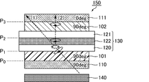
- the substrate 120 includes a thin film transistor (TFT) and a color filter layer.
- TFT thin film transistor
- the axial angles of the first polarizer 110 and the second polarizer 111 are set to 90 ° and 0 ° azimuth, respectively.
- the in-plane slow axes of the birefringent layers 101 and 102 are both set to 90 ° azimuth.
- a point P0 representing the polarization state of light after passing through the polarizer 1 passes through the birefringent layer 101, passes through the liquid crystal layer 122, passes through P2, and passes through the birefringent layer 102 through P3. Converted.
- the point P3 representing this polarization state coincides with the point E representing the polarization state of the extinction position when viewed from an oblique direction of 45 ° and polar angle 60 ° of the second polarizer 111.
- Light incident from an oblique direction with an angle of 60 ° is finally absorbed by the second polarizer 111. That is, the original function of the birefringent layer, which reduces the light leakage from the oblique direction and widens the viewing angle, is working normally.
- the point P0 representing the polarization state of the light after passing through the first polarizer 110 is converted to P1 by transmitting through the birefringent layer 101, and then scattered by the lower substrate 120, so that the traveling direction in the normal direction.
- the point representing the polarization state remains P1 even after scattering and progressing in the normal direction.
- the liquid crystal layer 122 VA liquid crystal layer
- the polarization state conversion is not performed for the incidence in the normal direction, and thus the point P2 representing the polarization state after passing through it. Does not change from P1.
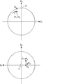
- the amount of light leakage increases as the distance between the point P3 and the point E ′ increases. More precisely, it is proportional to sin 2 ((1/2) ⁇ ⁇ P3OE ′) (the point O represents the center of the Poincare sphere. Also, since P3 and E ′ are points on the Poincare sphere, Note that the angle must not be measured in a projection map such as in Fig. 15).
- ⁇ PnOE ′ is not changed before and after the conversion.
- the birefringent layer 102 and the comparative example 1 are not limited to the birefringent layer (retardation film) of the VA mode. Since it is arranged perpendicularly or parallel to the absorption axis of the child, the polarization conversion by the retardation film after the traveling direction has changed to the normal direction due to scattering is all rotational movement about the S2 axis on the Poincare sphere. .
- the amount of light leakage from the second polarizer after scattering does not require an accurate determination of the polarization state Pn immediately before incidence on the second polarizer (P1 in the case of comparative form 1) If you know, you can estimate. It may be considered that the light leakage amount is small as P1 is close to E ′, and the light leakage amount is increased as P1 is separated from E ′. If P1 overlaps with E ′, the amount of light leakage is minimized.
- the substrate 120 includes a thin film transistor (TFT) and a color filter layer.
- TFT thin film transistor
- the axial angles of the first polarizer 110 and the second polarizer 111 are set to 90 ° and 0 ° azimuth, respectively.
- the in-plane slow axis of the birefringent layer 103 is set to 90 ° azimuth, and the in-plane slow axis of the birefringent layer 104 is set to 0 ° azimuth.
- the point P3 indicating the polarization state of the light of the above (2) scattered by the lower substrate 120 of the liquid crystal cell 130 and changing the traveling direction to the normal direction of the second polarizer 111 is Since it does not coincide with the point E ′ representing the polarization state of the extinction position in the normal direction of the second polarizer 111, light incident from an oblique direction of 45 ° and polar angle of 60 ° is scattered by the lower substrate of the liquid crystal panel.
- the traveling direction is changed to the linear direction, the second polarizer 111 eventually leaks light. That is, the CR is lower than that of the liquid crystal display device of the embodiment. Further, even when compared with the liquid crystal display device of Comparative Example 1, the distance between P3 and E ′ is large and the CR is low.
- the substrate 120 includes a thin film transistor (TFT) and a color filter layer.
- TFT thin film transistor
- the axial angles of the first polarizer 110 and the second polarizer 111 are set to 90 ° and 0 ° azimuth, respectively.
- the in-plane slow axis of the birefringent layer 105 is set to 0 ° azimuth, and the in-plane slow axis of the birefringent layer 106 is set to 90 ° azimuth.
- the point P3 indicating the polarization state of the light of the above (2) scattered by the lower substrate 120 of the liquid crystal cell 130 and changing the traveling direction to the normal direction of the second polarizer 111 is Since it does not coincide with the point E ′ representing the polarization state of the extinction position in the normal direction of the second polarizer 111, light incident from an oblique direction of 45 ° and polar angle of 60 ° is scattered by the lower substrate of the liquid crystal panel.
- the traveling direction is changed to the linear direction, the second polarizer 111 eventually leaks light. That is, the CR is lower than that of the liquid crystal display device of the embodiment. Further, even when compared with the liquid crystal display device of Comparative Example 1, the distance between P3 and E ′ is large and the CR is low.
- Example 1 As the liquid crystal display device of Example 1, the liquid crystal display device 50 of Embodiment 1 was actually manufactured.
- NB norbornene
- a negative C plate having an Rth of ⁇ 270 nm was used.
- Polyimide (PI) was used as a material for this birefringent layer.
- a material for the birefringent layer norbornene (NB) was used.
- NB norbornene
- the liquid crystal cell 30 a liquid crystal cell mounted on a Samsung liquid crystal television (trade name: UN46C7000) having a COA structure was used. The Rth at the time of black display with no voltage applied to the liquid crystal cell was 272 nm.
- Example 2 (Examples 2 to 4 and Comparative Examples 1 to 3) The liquid crystal display device of Example 1 except that at least one of the in-plane retardation (R), thickness direction retardation (Rth), and NZ coefficient (NZ) of the first type birefringent layers 1 and 3 is changed.
- liquid crystal display devices of Examples 2 to 4 and Comparative Examples 1 to 3 were produced.
- NZ 0.9 birefringent layer was used.
- Example 5 As the liquid crystal display device of Example 5, the liquid crystal display device 51 of Embodiment 2 was actually manufactured.
- norbornene (NB) As a material for the birefringent layer, norbornene (NB) was used.
- norbornene (NB) was used as a material for the birefringent layer. The rest is the same as the first embodiment.
- Example 6 (Examples 6 to 8 and Comparative Examples 4 to 6) The liquid crystal display device of Example 5 except that at least one of the in-plane retardation (R), thickness direction retardation (Rth), and NZ coefficient (NZ) of the first type birefringent layers 4 and 6 is changed.
- liquid crystal display devices of Examples 6 to 8 and Comparative Examples 4 to 6 were produced.
- Comparative Example 7 As a liquid crystal display device of Comparative Example 7, a liquid crystal display device 150 of Comparative Example 1 was actually manufactured.
- TAC triacetyl cellulose
- As a material for the birefringent layer norbornene (NB) was used. The rest is the same as the first embodiment.
- CR ratio measurement method for liquid crystal display devices The measurement was performed using an ultra-low luminance spectroradiometer (manufactured by TOPCON, trade name: SR-Ul1). The luminance of white display and black display in the normal direction was measured, and the ratio was taken as CR.
- the contrast ratio was 7000 or more.
- the contrast ratio was less than 7000.
- Visual evaluation also confirmed that the liquid crystal display devices of Examples 1 to 8 had higher CR than the liquid crystal display devices of Comparative Examples 1 to 9.
Abstract
The present invention provides a liquid crystal display device which is suppressed in light leakage and has improved CR. One embodiment of the present invention is a liquid crystal display device which is sequentially provided with a first polarizer, a first birefringent layer of a first type, a liquid crystal cell and a second polarizer in this order from the back surface side. The liquid crystal cell comprises a pair of substrates that face each other and a liquid crystal layer that is held between the substrates. The in-plane slow axis of the first birefringent layer of a first type is substantially parallel to the absorption axis of the second polarizer, and the absorption axis of the first polarizer is substantially perpendicular to the absorption axis of the second polarizer. When the NZ coefficient of the first birefringent layer of a first type is represented by NZ11 and the in-plane retardation is represented by R11, (1) 0 < NZ11 ≤ 0.5 and (2) 220 nm ≤ R11 ≤ 320 nm are satisfied.
Description
本発明は、液晶表示装置に関する。より詳しくは、偏光子と複屈折層とを備えた液晶表示装置に関するものである。
The present invention relates to a liquid crystal display device. More specifically, the present invention relates to a liquid crystal display device including a polarizer and a birefringent layer.
液晶表示装置は、通常、液晶パネル、バックライトとともに、偏光板、位相差フィルム(複屈折層)等の光学素子を含んで構成される。液晶パネルは、液晶層が観察者側と背面側との上下基板によって挟持されており、これら基板に光学的特性を向上させるための光学素子が載置されている。このような液晶表示装置は、その優れた表示特性から、モニター、プロジェクタ、携帯電話、携帯情報端末(PDA)等の電子機器に幅広く利用されている。
A liquid crystal display device is usually configured to include an optical element such as a polarizing plate and a retardation film (birefringent layer) together with a liquid crystal panel and a backlight. In the liquid crystal panel, a liquid crystal layer is sandwiched between upper and lower substrates on the viewer side and the back side, and optical elements for improving optical characteristics are placed on these substrates. Such liquid crystal display devices are widely used in electronic devices such as monitors, projectors, cellular phones, and personal digital assistants (PDAs) because of their excellent display characteristics.
また、液晶層を挟持する基板のうち、背面側の基板にカラーフィルタと薄膜トランジスタ(TFT:Thin Film Transistor)とが設けられたカラーフィルタ・オン・アレイ(COA:Color-filter On Array)構造の液晶表示装置が知られている(例えば、非特許文献1及び2参照。)。
In addition, among the substrates sandwiching the liquid crystal layer, a liquid crystal having a color filter on array (COA) structure in which a color filter and a thin film transistor (TFT: Thin Film Transistor) are provided on the back substrate. Display devices are known (for example, see Non-Patent Documents 1 and 2).
ところで、液晶表示装置(液晶パネル)には、黒表示における光漏れと、それによりコントラスト比(以下では、「CR」ともいう。また、特に断りがなければ、「CR」とは、液晶パネルの基板平面に対して法線方向のCRをいう。)が低いという課題がある。製品化されている液晶パネルの単体のCR(以下では、「ネイティブCR」ともいう。)は3000~5000である。
By the way, in a liquid crystal display device (liquid crystal panel), light leakage in black display and thereby a contrast ratio (hereinafter also referred to as “CR”. Unless otherwise specified, “CR” means “CR”. There is a problem that CR in the normal direction with respect to the substrate plane is low. The single CR (hereinafter also referred to as “native CR”) of the liquid crystal panel that has been commercialized is 3000 to 5000.
これに対して、映像の明暗に合わせてバックライト輝度の明暗をダイナミックに調整し、液晶表示装置のCR(以下では、「ダイナミックCR」ともいう)を向上させるディミング・バックライトが知られており、ダイナミックCRが10000以上の液晶表示装置が知られている。
On the other hand, a dimming backlight that improves the CR (hereinafter also referred to as “dynamic CR”) of a liquid crystal display device by dynamically adjusting the brightness of the backlight brightness according to the brightness of the image is known. A liquid crystal display device having a dynamic CR of 10,000 or more is known.
しかし、ディミング・バックライトによるCR改善効果は、映像の種類によっては限定的であるか、或いは、全く効果が得られない点で改善の余地があった。例えば、星空、映画の字幕、白黒の市松模様等、同一フレーム内に真黒と真白が混在する映像を表示する場合、白表示の白さが犠牲になるため、バックライト輝度を低減させることができない。バックライトをその輝度を独立に制御できる複数のブロックに分割し、ブロック毎に調光を行うローカル・ディミング・バックライトによりこの問題は多少改善されるが、ブロック内部では上記事情は変わりないので相変わらず効果は限定的であるといえる。また、ディミング・バックライトを導入することで、コストアップを伴う点でも改良の余地があった。このような状況下、液晶パネルのネイティブCRの改善が望まれている。
However, the CR improvement effect due to the dimming backlight is limited depending on the type of video, or there is room for improvement in that no effect can be obtained. For example, when displaying a video with a mixture of pure black and pure white within the same frame, such as a starry sky, movie subtitles, and black and white checkered patterns, the white brightness of the white display is sacrificed and the backlight luminance cannot be reduced. . This problem is somewhat improved by the local dimming backlight that divides the backlight into multiple blocks whose brightness can be controlled independently, and dimming each block, but the above situation does not change inside the block, so it remains the same. It can be said that the effect is limited. Moreover, there was room for improvement in terms of cost increase by introducing dimming backlight. Under such circumstances, it is desired to improve the native CR of the liquid crystal panel.
本発明は、上記現状に鑑みてなされたものであり、光漏れを抑制しCRを改善できる液晶表示装置を提供することを目的とするものである。
The present invention has been made in view of the above situation, and an object of the present invention is to provide a liquid crystal display device capable of suppressing light leakage and improving CR.
本発明者らは、液晶表示装置において、CRが低下する原因について、検討した結果、(I)偏光板性能が完全ではないことによる光漏れ、及び、(II)液晶パネル内部(下基板、液晶層、上基板)の光散乱による光漏れが原因であることを見出した。ただし、現在の液晶パネルに使用される典型的な偏光板のCRは10000~30000であるので、液晶パネルのCRが3000~5000であることの主要因は上記(II)にあると考えてよい。
As a result of examining the cause of the decrease in CR in the liquid crystal display device, the present inventors have found that (I) light leakage due to incomplete polarizing plate performance, and (II) the inside of the liquid crystal panel (lower substrate, liquid crystal It was found that light leakage due to light scattering of the layer and the upper substrate was the cause. However, since the CR of a typical polarizing plate used in a current liquid crystal panel is 10,000 to 30,000, it can be considered that the main factor that the CR of the liquid crystal panel is 3000 to 5000 is the above (II). .
上記(II)の液晶パネル内部の光散乱による光漏れについて、非特許文献1及び2には、光散乱によりパネル法線方向で観測される光漏れを詳細に分析した結果、液晶パネルに斜め入射した光がパネルの内部散乱により法線方向に進行方向を変え、観察面側の偏光子で十分に吸収されないことで光漏れになることが示されている。図22を用いて、より具体的に説明する。図22中の(1)に示すように、まず、液晶パネル(液晶セル)230への斜め入射光が位相差フィルムや液晶で楕円偏光に変調される。その後、(2)に示すように、散乱により進行方向を法線方向に変える(散乱前後で偏光状態は殆ど変化しない)。そして、(3)に示すように、楕円偏光のまま偏光板211に到達し偏光板211を透過するため、楕円率に応じて光漏れとして観測されることとなる。すなわち、散乱の前後で一般に偏光状態は変わらず、散乱後に透過する垂直配向(VA:Vertical Alignment)モードの液晶層、位相差フィルムも法線方向に進行する光に対しては全く偏光状態を変化させない、又は、変化させる場合も観察面側の偏光子での光漏れは全く同一になる別の偏光状態への変換を行うだけなので、結局、観察面側の偏光子での光漏れ量は散乱が起こる直前の偏光状態に依存する。そして、その散乱が起こる直前の偏光状態とは、偏光板(偏光子)の構成、及び、位相差フィルムの特性値に依存する。
Regarding the light leakage due to light scattering inside the liquid crystal panel of (II) above, Non-Patent Documents 1 and 2 show that the light leakage observed in the normal direction of the panel due to light scattering is analyzed in detail, and is incident obliquely on the liquid crystal panel. It is shown that the light travels in the normal direction due to the internal scattering of the panel and is not absorbed sufficiently by the polarizer on the observation surface side, resulting in light leakage. This will be described more specifically with reference to FIG. As shown in (1) in FIG. 22, first, obliquely incident light on the liquid crystal panel (liquid crystal cell) 230 is modulated into elliptically polarized light by a retardation film or liquid crystal. Thereafter, as shown in (2), the traveling direction is changed to the normal direction by scattering (the polarization state hardly changes before and after scattering). Then, as shown in (3), since the light reaches the polarizing plate 211 and passes through the polarizing plate 211 as elliptically polarized light, light leakage is observed according to the ellipticity. In other words, the polarization state generally does not change before and after scattering, and the vertical alignment (VA: Vertical Alignment) mode liquid crystal layer and retardation film transmitted after scattering also change the polarization state completely for light traveling in the normal direction. Even if it is not changed or changed, the light leakage at the polarizer on the observation surface side is simply converted to another polarization state where the light leakage is exactly the same. Depends on the polarization state just before occurs. And the polarization state immediately before the scattering occurs depends on the configuration of the polarizing plate (polarizer) and the characteristic value of the retardation film.
この点について、非特許文献1及び2には、カラーフィルタ・オン・アレイ(COA)構造を有するVAモードの液晶パネルの背面側(下基板側)の位相差フィルムの位相差値(|Rth|)を小さめに調整することが記載されている。これにより、下基板に斜め入射した光が散乱により法線方向に進行方向を変えたとしても、観察面側(上基板側)の偏光子で大部分が吸収されるため光漏れとなりにくく、位相差値の大きな位相差フィルムを下基板側に用いた従来の液晶表示装置と比べて高CRが得られる。なお、COA構造の液晶パネルにおいては、入射光の散乱の主な原因となるカラーフィルタが下基板側に設けられており、下基板での入射光の散乱が、上基板での散乱よりも大きくなるが、上基板での散乱が下基板での散乱に比べて大きい液晶パネルにおいては、位相差フィルムの位相差値を小さめに調整しても充分なCR改善効果は得られない。なぜなら、偏光子により、下基板入射時に法線方向に散乱しても光漏れしにくい偏光状態であったとしても、VA液晶層を通過前後で偏光状態が大きく変化するので、上基板入射時に法線方向に散乱すると逆に光漏れとなりやすい偏光状態に変化してしまうからである。すなわち、下基板散乱での光漏れは従来と比べて減るが、上基板散乱での光漏れは従来と比べて増える。上基板での散乱が下基板でのそれに比べて小さいパネルでは、上基板入射時に散乱が起こった場合にその光が上基板側の偏光子から漏れやすいという事実は変わらないが、そもそも上基板での散乱が起こりにくいので、上基板からの光漏れと下基板からの光漏れの総量は従来と比べて減るのである。
In this regard, Non-Patent Documents 1 and 2 describe the retardation value (| Rth |) of the retardation film on the back side (lower substrate side) of the VA mode liquid crystal panel having a color filter on array (COA) structure. ) Is adjusted to be smaller. As a result, even if light obliquely incident on the lower substrate changes its traveling direction in the normal direction due to scattering, most of the light is absorbed by the polarizer on the observation surface side (upper substrate side), so light leakage is unlikely. High CR can be obtained as compared with a conventional liquid crystal display device using a retardation film having a large retardation value on the lower substrate side. In the liquid crystal panel having the COA structure, a color filter that is a main cause of scattering of incident light is provided on the lower substrate side, and the scattering of incident light on the lower substrate is larger than the scattering on the upper substrate. However, in a liquid crystal panel in which scattering on the upper substrate is larger than that on the lower substrate, even if the retardation value of the retardation film is adjusted to be small, a sufficient CR improvement effect cannot be obtained. This is because the polarization state changes greatly before and after passing through the VA liquid crystal layer even if it is in a polarization state in which light does not leak even if it is scattered in the normal direction when the lower substrate is incident due to the polarizer. This is because, if the light is scattered in the linear direction, it changes to a polarization state that tends to cause light leakage. That is, light leakage due to lower substrate scattering is reduced as compared with the conventional case, but light leakage due to upper substrate scattering is increased as compared with the conventional case. In the panel where the scattering on the upper substrate is smaller than that on the lower substrate, the fact that the light is likely to leak from the polarizer on the upper substrate side when scattering occurs at the time of incidence on the upper substrate does not change, but in the first place Therefore, the total amount of light leakage from the upper substrate and light leakage from the lower substrate is reduced as compared with the conventional case.
本発明者らが、上記非特許文献1及び2に記載の液晶表示装置(液晶パネル)について精査したところ、位相差値の大きな位相差フィルムを下側に用いた従来構成と比べてCRは改善されるものの、斜め方向からの入射し、法線方向に散乱した光の漏れが充分には抑制されておらず、観察面側の偏光子から光漏れが生じている点で改善の余地があることが判明した。
When the present inventors scrutinized the liquid crystal display devices (liquid crystal panels) described in Non-Patent Documents 1 and 2 above, CR was improved compared to the conventional configuration using a retardation film having a large retardation value on the lower side. However, leakage of light incident from an oblique direction and scattered in the normal direction is not sufficiently suppressed, and there is room for improvement in that light leakage occurs from the polarizer on the observation surface side. It has been found.
本発明者らは、更に、鋭意検討したところ、斜め方向からの入射光の偏光状態と、観察面側の偏光子を法線方向から見た場合の消光位に相当する偏光状態とのずれに応じて、斜め方向から入射し、観察面側の偏光子の法線方向に散乱した光が光漏れとして射出されることを見出した。そして、下基板に斜め入射する光の偏光状態が観察面側の偏光子を法線方向から見た場合の該偏光子の消光位に相当する偏光状態と実質的に一致するように、背面側の位相差フィルム(複屈折層)の位相差値を調整することで、下基板に斜め入射した光が散乱により法線方向に進行方向を変えたとしても観察面側の偏光子で充分に吸収されることを見いだし、上記課題をみごとに解決することができることに想到し、本発明に到達したものである。
The inventors of the present invention have made further studies and found that the polarization state of the incident light from the oblique direction is different from the polarization state corresponding to the extinction position when the polarizer on the observation surface side is viewed from the normal direction. Accordingly, it has been found that light incident from an oblique direction and scattered in the normal direction of the polarizer on the observation surface side is emitted as light leakage. And the back side so that the polarization state of light obliquely incident on the lower substrate substantially coincides with the polarization state corresponding to the extinction position of the polarizer when the polarizer on the observation surface side is viewed from the normal direction By adjusting the retardation value of the retardation film (birefringent layer), even if the light obliquely incident on the lower substrate changes its traveling direction in the normal direction due to scattering, it is sufficiently absorbed by the polarizer on the observation surface side As a result, the inventors have arrived at the present invention by conceiving that the above problems can be solved brilliantly.
すなわち、本発明の一態様は、第一偏光子、1又は2以上の第一の複屈折層(位相差フィルム)、液晶セル、及び、第二偏光子を背面側からこの順に備える液晶表示装置であって、前記液晶セルは、対向する一対の基板(下基板及び上基板)と、両基板間に挟持された液晶層とを含み、前記第一偏光子の吸収軸は、前記第二偏光子の吸収軸と実質的に直交し、前記液晶表示装置が2以上の第一の複屈折層を備える場合、前記2以上の第一の複屈折層は、NZ係数及び位相差の少なくとも一方が互いに異なる複数の複屈折層を含み、前記1又は2以上の第一の複屈折層は、前記第一偏光子を通過し、斜め方向から入射した光の偏光状態を前記第二偏光子の法線方向から見た場合の消光位の偏光状態に変換する液晶表示装置(以下では、「本発明の第一の液晶表示装置」ともいう)である。
That is, one embodiment of the present invention is a liquid crystal display device including a first polarizer, one or more first birefringent layers (retardation film), a liquid crystal cell, and a second polarizer in this order from the back side. The liquid crystal cell includes a pair of opposing substrates (a lower substrate and an upper substrate) and a liquid crystal layer sandwiched between the substrates, and the absorption axis of the first polarizer is the second polarization When the liquid crystal display device includes two or more first birefringent layers substantially orthogonal to the absorption axis of the child, the two or more first birefringent layers have at least one of an NZ coefficient and a phase difference. A plurality of different birefringent layers are included, and the one or more first birefringent layers pass through the first polarizer, and the polarization state of light incident from an oblique direction is determined by the method of the second polarizer. A liquid crystal display device (hereinafter referred to as “the present invention”) that converts the polarization state to the extinction level when viewed from the line direction. The first liquid crystal display device of the "to be also referred to).
前記「斜め方向から入射した光」とは、具体的には、第一偏光子の吸収軸方向を方位0°及び180°と定義した時に、方位45°±22.5°の範囲、方位135°±22.5°、方位225°±22.5°の範囲又は方位315°±22.5°の範囲から入射した光である。
The “light incident from an oblique direction” specifically refers to an azimuth range of 45 ° ± 22.5 ° and an azimuth direction 135 when the absorption axis direction of the first polarizer is defined as azimuths of 0 ° and 180 °. The light is incident from the range of ± 22.5 ° and the direction of 225 ° ± 22.5 ° or the range of 315 ° ± 22.5 °.
前記「入射した光の偏光状態を第二偏光子の法線方向から見た場合の消光位に変換する」とは、換言すれば、入射した光(偏光)の偏光状態を直線偏光に変換(または保持)し、そしてその振動方向を第二偏光子の吸収軸方向に実質的に一致させることと言えるが、必ずしも厳密に一致させる必要はない。ここで、実質的に一致とは、半径1のポアンカレ球上における2点間の距離が0.15以下の状態を指す。また、第一の複屈折層によって変換された光の偏光状態が完全な直線偏光ではなく、楕円偏光であっても良い。
In other words, “converting the polarization state of incident light into an extinction level when viewed from the normal direction of the second polarizer” means, in other words, converting the polarization state of incident light (polarized light) into linearly polarized light ( It can be said that the vibration direction is substantially matched with the absorption axis direction of the second polarizer. Here, “substantially coincide” refers to a state where the distance between two points on a Poincare sphere having a radius of 1 is 0.15 or less. Further, the polarization state of the light converted by the first birefringent layer may be elliptical polarization instead of perfect linear polarization.
本発明の第一の液晶表示装置の構成としては、このような構成要素を必須として形成されるものである限り、その他の構成要素により特に限定されるものではない。
The configuration of the first liquid crystal display device of the present invention is not particularly limited by other components as long as such components are essential.
なお、上述のような偏光変換を行い得る限り、第一の複屈折層の種類(NZ係数)、数、位相差値、材質等は適宜選択することができ、例えば、第一の複屈折層は、単一(一枚)の複屈折層のみからなる形態であってもよいし、NZ係数及び位相差の少なくとも一方が互いに異なる複数の複屈折層のみからなる形態であってもよい。更に、NZ係数及び位相差が同じ複数の複屈折層と、該複数の複屈折層とはNZ係数及び位相差の少なくとも一方が異なる少なくとも一枚の複屈折層とを含む形態(より具体的には、例えば、2枚の同じポジティブCプレートと1枚のポジティブAプレートとを含む形態等)であってもよい。特に、第一種の複屈折層を含む形態、第二種の複屈折層及び第四種の複屈折層を含む形態、第三種の複屈折層及び第五種の複屈折層を含む形態が好適であり、このような複屈折層を含む液晶表示装置もまた本発明の一つの態様である。すなわち、本発明の別の態様は、第一偏光子、第一の第一種の複屈折層、液晶セル(液晶パネル)、及び、第二偏光子を背面側からこの順に備える液晶表示装置であって、前記液晶セルは、対向する一対の基板(下基板及び上基板)と、両基板間に挟持された液晶層とを含み、前記第一の第一種の複屈折層の面内遅相軸は、前記第二偏光子の吸収軸と実質的に平行であり、前記第一偏光子の吸収軸は、前記第二偏光子の吸収軸と実質的に直交し、前記第一の第一種の複屈折層のNZ係数をNZ11、面内位相差をR11としたとき、下記式(2-1)及び(2-2)を満たす液晶表示装置(以下では、「本発明の第二の液晶表示装置」ともいう)である。
0<NZ11≦0.5 (2-1)
220nm≦R11≦320nm (2-2) As long as the above-described polarization conversion can be performed, the type (NZ coefficient), number, retardation value, material, and the like of the first birefringent layer can be appropriately selected. For example, the first birefringent layer May be a form consisting of only a single (one) birefringent layer, or may be a form consisting of only a plurality of birefringent layers having different NZ coefficients and phase differences from each other. Furthermore, a form (more specifically, including a plurality of birefringent layers having the same NZ coefficient and retardation, and at least one birefringent layer having at least one of the NZ coefficient and the phase difference different from the plurality of birefringent layers. May be, for example, a form including two identical positive C plates and one positive A plate). In particular, a form including a first birefringent layer, a form including a second birefringent layer and a fourth birefringent layer, a form including a third birefringent layer and a fifth birefringent layer A liquid crystal display device including such a birefringent layer is also an embodiment of the present invention. That is, another aspect of the present invention is a liquid crystal display device including a first polarizer, a first first-type birefringent layer, a liquid crystal cell (liquid crystal panel), and a second polarizer in this order from the back side. The liquid crystal cell includes a pair of opposing substrates (a lower substrate and an upper substrate) and a liquid crystal layer sandwiched between the substrates, and an in-plane retardation of the first first-type birefringent layer. The phase axis is substantially parallel to the absorption axis of the second polarizer, the absorption axis of the first polarizer is substantially orthogonal to the absorption axis of the second polarizer, and the first first When a NZ coefficient of a birefringent layer is NZ11 and an in-plane retardation is R11, a liquid crystal display device satisfying the following formulas (2-1) and (2-2) (hereinafter referred to as “second embodiment of the present invention”). It is also referred to as a “liquid crystal display device”.
0 <NZ11 ≦ 0.5 (2-1)
220 nm ≦ R11 ≦ 320 nm (2-2)
本発明の第二の液晶表示装置によっても、本発明の第一の液晶表示装置と同様に、下基板に斜め入射した光が散乱により法線方向に進行方向を変えたとしても観察面側の偏光子で充分に吸収され、大きなCR改善効果が得られる。また、複数種の複屈折層を組み合わせる形態に比べ、製造工程を簡略化できるとともに、薄型化を図ることもできる。なお、複数種の複屈折層を組み合わせる形態によれば、各複屈折層を容易に製造することができる。
Even in the second liquid crystal display device of the present invention, similarly to the first liquid crystal display device of the present invention, even if light obliquely incident on the lower substrate changes its traveling direction in the normal direction due to scattering, It is sufficiently absorbed by the polarizer, and a large CR improvement effect is obtained. In addition, the manufacturing process can be simplified and the thickness can be reduced as compared with the case where a plurality of types of birefringent layers are combined. In addition, according to the form which combines multiple types of birefringent layers, each birefringent layer can be manufactured easily.
本発明の第二の液晶表示装置の構成としては、このような構成要素を必須として形成されるものである限り、その他の構成要素により特に限定されるものではない。
The configuration of the second liquid crystal display device of the present invention is not particularly limited by other components as long as such components are essential.
また、本発明の更に別の態様は、第一偏光子、第一の第一種の複屈折層、液晶セル(液晶パネル)、及び、第二偏光子を背面側からこの順に有する液晶表示装置であって、前記液晶セルは、対向する一対の基板(下基板及び上基板)と、両基板間に挟持された液晶層とを含み、前記第一の第一種の複屈折層の面内遅相軸は、前記第二偏光子の吸収軸と実質的に直交し、前記第一偏光子の吸収軸は、前記第二偏光子の吸収軸と実質的に直交し、前記第一の第一種の複屈折層のNZ係数をNZ11、面内位相差をR11としたとき、下記式(3-1)及び(3-2)を満たす液晶表示装置(以下では、「本発明の第三の液晶表示装置」ともいう)である。
0.5≦NZ11<1.0 (3-1)
220nm≦R11≦320nm (3-2) Still another embodiment of the present invention is a liquid crystal display device having a first polarizer, a first first-type birefringent layer, a liquid crystal cell (liquid crystal panel), and a second polarizer in this order from the back side. The liquid crystal cell includes a pair of opposing substrates (a lower substrate and an upper substrate) and a liquid crystal layer sandwiched between both substrates, and the in-plane of the first type birefringent layer. The slow axis is substantially perpendicular to the absorption axis of the second polarizer, the absorption axis of the first polarizer is substantially perpendicular to the absorption axis of the second polarizer, and the first first When a NZ coefficient of a birefringent layer is NZ11 and an in-plane retardation is R11, a liquid crystal display device satisfying the following formulas (3-1) and (3-2) (hereinafter referred to as “third embodiment of the present invention”). It is also referred to as a “liquid crystal display device”.
0.5 ≦ NZ11 <1.0 (3-1)
220 nm ≦ R11 ≦ 320 nm (3-2)
本発明の第三の液晶表示装置によっても、本発明の第一及び第二の液晶表示装置と同様に、下基板に斜め入射した光が散乱により法線方向に進行方向を変えたとしても観察面側の偏光子で充分に吸収され、大きなCR改善効果が得られる。また、複数種の複屈折層を組み合わせる形態に比べ、製造工程を簡略化できるとともに、薄型化を図ることもできる。
As with the first and second liquid crystal display devices of the present invention, the third liquid crystal display device of the present invention is also observed even when light obliquely incident on the lower substrate changes its traveling direction in the normal direction due to scattering. It is sufficiently absorbed by the surface-side polarizer, and a large CR improvement effect is obtained. In addition, the manufacturing process can be simplified and the thickness can be reduced as compared with the case where a plurality of types of birefringent layers are combined.
本発明の第三の液晶表示装置の構成としては、このような構成要素を必須として形成されるものである限り、その他の構成要素により特に限定されるものではない。
The configuration of the third liquid crystal display device of the present invention is not particularly limited by other components as long as such components are formed as essential.
本発明の第一~第三の液晶表示装置における好ましい形態について以下に詳しく説明する。
Preferred embodiments of the first to third liquid crystal display devices of the present invention will be described in detail below.
本発明の第一の液晶表示装置は、更に、前記液晶セル及び前記第二偏光子の間に、1又は2以上の第二の複屈折層を備え、前記液晶表示装置が2以上の第二の複屈折層を備える場合、前記2以上の第二の複屈折層は、NZ係数及び位相差の少なくとも一方が互いに異なる複数の複屈折層を含み、前記液晶層、及び、前記1又は2以上の第二の複屈折層は、黒表示時において、法線方向から入射した光の偏光状態を実質的に変更しないことが好ましい。これにより、第二偏光子の消光位の偏光状態に変換された光が液晶表示装置内部で、法線方向に散乱しても、第二偏光子に吸収させることができるので、本発明のCR改善効果を高めることができる。
The first liquid crystal display device of the present invention further includes one or two or more second birefringent layers between the liquid crystal cell and the second polarizer, and the liquid crystal display device has two or more second birefringent layers. When the birefringent layer is provided, the two or more second birefringent layers include a plurality of birefringent layers having different NZ coefficients and retardations, the liquid crystal layer, and the one or more birefringent layers. The second birefringent layer preferably does not substantially change the polarization state of light incident from the normal direction during black display. As a result, even if the light converted into the polarization state of the extinction position of the second polarizer is scattered in the normal direction inside the liquid crystal display device, it can be absorbed by the second polarizer. The improvement effect can be enhanced.
なお、上述のような特性を発揮し得る限り、第二の複屈折層の種類(NZ係数)、数、位相差値、材質等は適宜選択することができ、例えば、第二の複屈折層は、単一(一枚)の複屈折層のみからなる形態であってもよいし、NZ係数及び位相差の少なくとも一方が互いに異なる複数の複屈折層のみからなる形態であってもよい。更に、NZ係数及び位相差が同じ複数の複屈折層と、該複数の複屈折層とはNZ係数及び位相差の少なくとも一方が異なる少なくとも一枚の複屈折層とを含む形態(より具体的には、例えば、2枚の同じポジティブCプレートと1枚のポジティブAプレートとを含む形態等)であってもよい。特に、第一種の複屈折層を含む形態、第二種の複屈折層及び第四種の複屈折層を含む形態、第三種の複屈折層及び第五種の複屈折層を含む形態が好適である。
As long as the above-described characteristics can be exhibited, the type (NZ coefficient), number, retardation value, material, and the like of the second birefringent layer can be appropriately selected. For example, the second birefringent layer May be a form consisting of only a single (one) birefringent layer, or may be a form consisting of only a plurality of birefringent layers having different NZ coefficients and phase differences from each other. Furthermore, a form (more specifically, including a plurality of birefringent layers having the same NZ coefficient and retardation, and at least one birefringent layer having at least one of the NZ coefficient and the phase difference different from the plurality of birefringent layers. May be, for example, a form including two identical positive C plates and one positive A plate). In particular, a form including a first birefringent layer, a form including a second birefringent layer and a fourth birefringent layer, a form including a third birefringent layer and a fifth birefringent layer Is preferred.
本発明の第二の液晶表示装置において、0.15≦NZ11≦0.35、及び、250nm≦R11≦290nmを満たすことが好ましい。これにより、下基板に斜め入射した光が散乱により法線方向に進行方向を変えたとしても観察面側の偏光子で充分に吸収され、より大きなCR改善効果が得られる。
In the second liquid crystal display device of the present invention, it is preferable that 0.15 ≦ NZ11 ≦ 0.35 and 250 nm ≦ R11 ≦ 290 nm are satisfied. As a result, even if light obliquely incident on the lower substrate changes its traveling direction in the normal direction due to scattering, it is sufficiently absorbed by the polarizer on the observation surface side, and a greater CR improvement effect is obtained.
本発明の第二の液晶表示装置は、更に、前記液晶セル及び前記第二偏光子の間に、第二種の複屈折層、及び、第二の第一種の複屈折層を前記液晶セル側からこの順に備え、黒表示時において前記液晶層中の液晶分子は、略垂直配向し、前記第二の第一種の複屈折層の面内遅相軸は、前記第二偏光子の吸収軸と実質的に平行であり、前記第二の第一種の複屈折層のNZ係数をNZ12、面内位相差をR12、前記第二種の複屈折層の厚み方向位相差をRth2、黒表示時における前記液晶セルの厚み方向位相差をRthlcとしたとき、下記式(2-3)~(2-5)を満たす形態(以下では、「第一形態」ともいう。)が好ましい。
0.5≦NZ12<1.0 (2-3)
220nm≦R12≦320nm (2-4)
-50nm≦Rth2+Rthlc≦50nm (2-5) The second liquid crystal display device of the present invention further includes a second type of birefringent layer and a second type of birefringent layer between the liquid crystal cell and the second polarizer. The liquid crystal molecules in the liquid crystal layer are substantially vertically aligned during black display, and the in-plane slow axis of the second first-type birefringent layer is the absorption of the second polarizer. It is substantially parallel to the axis, the NZ coefficient of the second type birefringent layer is NZ12, the in-plane retardation is R12, the thickness direction retardation of the second type birefringent layer is Rth2, black When the thickness direction retardation of the liquid crystal cell at the time of display is Rthlc, a form satisfying the following formulas (2-3) to (2-5) (hereinafter also referred to as “first form”) is preferable.
0.5 ≦ NZ12 <1.0 (2-3)
220 nm ≦ R12 ≦ 320 nm (2-4)
−50 nm ≦ Rth2 + Rthlc ≦ 50 nm (2-5)
なお、本明細書において、「黒表示時」とは、最低階調を表示する時のことをいう。
In the present specification, “when displaying black” means displaying the lowest gradation.
これにより、下基板に斜め入射した光であって、散乱せずに液晶パネル内を透過する光も観察面側の偏光子(第二偏光子)により、吸収することができるため、斜め方向からの光漏れを低減して視野角を拡大することができる。
Accordingly, light obliquely incident on the lower substrate and transmitted through the liquid crystal panel without being scattered can be absorbed by the polarizer (second polarizer) on the observation surface side. Can be reduced and the viewing angle can be expanded.
第一形態において、0.65≦NZ12≦0.85、及び、250nm≦R12≦290nmを満たすことが好ましく、-30nm≦Rth2+Rthlc≦30nmを満たすことが好ましい。これにより、斜め方向からの光漏れを一層低減して視野角を拡大することができる。
In the first embodiment, 0.65 ≦ NZ12 ≦ 0.85 and 250 nm ≦ R12 ≦ 290 nm are preferably satisfied, and −30 nm ≦ Rth2 + Rthlc ≦ 30 nm is preferably satisfied. Thereby, the light leakage from the oblique direction can be further reduced and the viewing angle can be expanded.
また、前記第二種の複屈折層のNZ係数をNZ2としたとき、第一形態において、5≦NZ2を満たすことが好ましく、10≦NZ2を満たすことがより好ましい。これにより、斜め方向からの光漏れを一層低減して視野角を拡大することができる。
Further, when the NZ coefficient of the second birefringent layer is NZ2, it is preferable that 5 ≦ NZ2 is satisfied in the first embodiment, and it is more preferable that 10 ≦ NZ2 is satisfied. Thereby, the light leakage from the oblique direction can be further reduced and the viewing angle can be expanded.
本発明の第三の液晶表示装置において、0.65≦NZ11≦0.85、及び、250nm≦R11≦290nmを満たすことが好ましい。これにより、下基板に斜め入射した光が散乱により法線方向に進行方向を変えたとしても観察面側の偏光子で充分に吸収され、より大きなCR改善効果が得られる。
In the third liquid crystal display device of the present invention, it is preferable that 0.65 ≦ NZ11 ≦ 0.85 and 250 nm ≦ R11 ≦ 290 nm are satisfied. As a result, even if light obliquely incident on the lower substrate changes its traveling direction in the normal direction due to scattering, it is sufficiently absorbed by the polarizer on the observation surface side, and a greater CR improvement effect is obtained.
本発明の第三の液晶表示装置は、更に、前記液晶セル及び前記第二偏光子の間に、第二種の複屈折層、及び、第二の第一種の複屈折層を前記液晶セル側からこの順に備え、黒表示時において前記液晶層中の液晶分子は、略垂直配向し、前記第二の第一種の複屈折層の面内遅相軸は、前記第二偏光子の吸収軸と実質的に直交し、前記第二の第一種の複屈折層のNZ係数をNZ12、面内位相差をR12、前記第二種の複屈折層の厚み方向位相差をRth2、黒表示時における前記液晶セルの厚み方向位相差をRthlcとしたとき、下記式(3-3)~(3-5)を満たす形態(以下では、「第二形態」ともいう。)が好ましい。
0<NZ12≦0.5 (3-3)
220nm≦R12≦320nm (3-4)
-50nm≦Rth2+Rthlc≦50nm (3-5) The third liquid crystal display device of the present invention further includes a second birefringent layer and a second first birefringent layer between the liquid crystal cell and the second polarizer. The liquid crystal molecules in the liquid crystal layer are substantially vertically aligned during black display, and the in-plane slow axis of the second first-type birefringent layer is the absorption of the second polarizer. Substantially perpendicular to the axis, the NZ coefficient of the second birefringent layer of the second type is NZ12, the in-plane retardation is R12, the thickness direction retardation of the second birefringent layer is Rth2, black display When the thickness direction retardation of the liquid crystal cell at this time is Rthlc, a form satisfying the following formulas (3-3) to (3-5) (hereinafter also referred to as “second form”) is preferable.
0 <NZ12 ≦ 0.5 (3-3)
220 nm ≦ R12 ≦ 320 nm (3-4)
−50 nm ≦ Rth2 + Rthlc ≦ 50 nm (3-5)
これにより、下基板に斜め入射した光であって、散乱せずに液晶パネル内を透過する光も観察面側の偏光子(第二偏光子)により、吸収することができるため、斜め方向からの光漏れを低減して視野角を拡大することができる。
Accordingly, light obliquely incident on the lower substrate and transmitted through the liquid crystal panel without being scattered can be absorbed by the polarizer (second polarizer) on the observation surface side. Can be reduced and the viewing angle can be expanded.
第二形態において、0.15≦NZ12≦0.35、及び、250nm≦R12≦290nmを満たすことが好ましく、-30nm≦Rth2+Rthlc≦30nmを満たすことが好ましい。これにより、斜め方向からの光漏れを一層低減して視野角を拡大することができる。
In the second embodiment, 0.15 ≦ NZ12 ≦ 0.35 and 250 nm ≦ R12 ≦ 290 nm are preferably satisfied, and −30 nm ≦ Rth2 + Rthlc ≦ 30 nm is preferably satisfied. Thereby, the light leakage from the oblique direction can be further reduced and the viewing angle can be expanded.
また、前記第二種の複屈折層のNZ係数をNZ2としたとき、第二形態において、5≦NZ2を満たすことが好ましく、10≦NZ2を満たすことがより好ましい。これにより、斜め方向からの光漏れを一層低減して視野角を拡大することができる。
Further, when the NZ coefficient of the second birefringent layer is NZ2, in the second embodiment, 5 ≦ NZ2 is preferably satisfied, and 10 ≦ NZ2 is more preferably satisfied. Thereby, the light leakage from the oblique direction can be further reduced and the viewing angle can be expanded.
本発明のCR改善効果を高める観点からは、本発明の第一~第三の液晶表示装置において、前記一対の基板のうち背面側を下基板、観察面側を上基板としたとき、前記上基板の散乱が前記下基板の散乱よりも小さい形態(以下では、「第三の形態」ともいう)が好ましい。ここで、上下基板の散乱の大小は、双方を同一のクロスニコル偏光板及びパラレルニコル偏光板の間に挟んで透過率測定、及び、コントラスト計算を行い、コントラストが低い方を散乱の大きい基板、コントラストが高い方を散乱の小さい基板と判別する。
From the viewpoint of enhancing the CR improvement effect of the present invention, in the first to third liquid crystal display devices of the present invention, when the back side of the pair of substrates is a lower substrate and the observation surface side is an upper substrate, the upper A form in which the scattering of the substrate is smaller than that of the lower substrate (hereinafter, also referred to as “third form”) is preferable. Here, the size of the scattering of the upper and lower substrates is determined by measuring the transmittance by sandwiching both of them between the same crossed Nicol polarizing plate and the parallel Nicol polarizing plate, and calculating the contrast. The higher one is discriminated as a substrate with less scattering.
第三形態を実現する観点からは、前記下基板は、カラーフィルタ(CF)層と薄膜トランジスタ(TFT)とを含み、前記液晶セルは、カラーフィルタ・オン・アレイ(COA)構造を有することが好ましく、前記液晶セルは、染料系カラーフィルタ層を含むことが好ましく、前記液晶セルは、カラーフィルタ層を含まないことが好ましい。なお、ここでいうTFTとは、TFT(トランジスタ)そのものだけではなく、TFT基板に一般的に備えられるその他の材料や構造物を含む広義のTFTを意味し、例えば、ゲート配線、ソース配線、Cs配線(補助容量)、有機絶縁膜、透明電極(ITO)、配向膜等を含む。現在、CF層としては一般的に顔料系CF層が用いられ、顔料系CF層とTFTは、共に入射光の散乱の大きな要因となり得るが、これらが下基板に集約されていることで、確実に上基板の散乱を下基板の散乱よりも小さくすることができる。TFTの中で特に散乱に影響を与えるのは、開口部(入射光が通過する領域)に露出した配線類である。なかでも、偏光子の吸収軸又は透過軸に対して平行でも直交でもない方位に伸びる配線が散乱(回折の場合もある)の原因になる。例えば、第一及び第二偏光子の吸収軸方位がそれぞれ0°及び90°の液晶表示装置において、45°方位に伸びるCs配線があると、Cs配線のエッジ部分が散乱や回折によって光って見えることがある。また、有機絶縁膜の膜質(表面凹凸の有無)等も散乱の大小に影響を与える可能性がある。また、上基板にCF層が設けられるとともに、下基板にTFTが設けられるとき、当該CF層を散乱が非常に少ないとされる染料系CF層とすることで、上基板の散乱をゼロに近づけ、上基板の散乱を下基板より小さくすることもできる。更に、CF層を設けず、かつ、下基板にTFTを設けることで、上基板の散乱をゼロに近づけ、上基板の散乱を下基板より小さくすることもできる。なお、CF層を含む基板は、BM(ブラックマトリクス)層、配向膜、透明電極(ITO)等の部材を含み得るが、これらによる散乱は、顔料系CF層のそれに比べて無視できる程に小さい。
From the viewpoint of realizing the third embodiment, the lower substrate preferably includes a color filter (CF) layer and a thin film transistor (TFT), and the liquid crystal cell preferably has a color filter on array (COA) structure. The liquid crystal cell preferably includes a dye-based color filter layer, and the liquid crystal cell preferably does not include a color filter layer. The TFT here means not only the TFT (transistor) itself but also a broad TFT including other materials and structures generally provided in the TFT substrate. For example, the gate wiring, the source wiring, Cs Including wiring (auxiliary capacitor), organic insulating film, transparent electrode (ITO), alignment film and the like. Currently, a pigment-based CF layer is generally used as the CF layer, and both the pigment-based CF layer and the TFT can be a major factor in the scattering of incident light. In addition, the scattering of the upper substrate can be made smaller than that of the lower substrate. Of the TFTs, the wirings exposed to the openings (regions through which incident light passes) particularly affect scattering. In particular, wiring extending in an orientation that is neither parallel nor orthogonal to the absorption axis or transmission axis of the polarizer causes scattering (may be diffraction). For example, in a liquid crystal display device in which the absorption axes of the first and second polarizers are 0 ° and 90 °, respectively, if there is a Cs wiring extending in the 45 ° azimuth, the edge portion of the Cs wiring appears to shine due to scattering or diffraction. Sometimes. In addition, the quality of the organic insulating film (the presence or absence of surface irregularities) and the like may affect the size of scattering. In addition, when a CF layer is provided on the upper substrate and a TFT is provided on the lower substrate, the scattering of the upper substrate is brought close to zero by making the CF layer a dye-based CF layer that has very little scattering. The scattering of the upper substrate can be made smaller than that of the lower substrate. Further, by providing the TFT on the lower substrate without providing the CF layer, the scattering of the upper substrate can be made close to zero and the scattering of the upper substrate can be made smaller than that of the lower substrate. The substrate including the CF layer may include a member such as a BM (black matrix) layer, an alignment film, and a transparent electrode (ITO), but scattering due to these is negligibly small compared to that of the pigment-based CF layer. .
本発明の第一、第二及び第三の液晶表示装置によれば、光漏れを抑制しCRを改善することができる。
According to the first, second and third liquid crystal display devices of the present invention, light leakage can be suppressed and CR can be improved.
本明細書において、偏光子は、無偏光(自然光)、部分偏光又は偏光から、特定方向にのみ振動する偏光(直線偏光)を取り出す機能を有するものである。特に断りのない限り、本明細書中で「偏光子」というときは保護フィルムを含まず、偏光機能を有する素子だけを指す。
In this specification, a polarizer has a function of extracting polarized light (linearly polarized light) that vibrates only in a specific direction from non-polarized light (natural light), partially polarized light, or polarized light. Unless otherwise specified, the term “polarizer” in this specification refers to only a device having a polarizing function without including a protective film.
面内位相差Rは、R=(ns-nf)×dで定義される。また、厚み方向位相差Rthは、Rth=(nz-(nx+ny)/2)×dで定義される。そして、NZ係数(2軸性パラメータ)は、NZ=(ns-nz)/(ns-nf)で定義される。
The in-plane retardation R is defined by R = (ns−nf) × d. The thickness direction retardation Rth is defined by Rth = (nz− (nx + ny) / 2) × d. The NZ coefficient (biaxial parameter) is defined by NZ = (ns−nz) / (ns−nf).
なお、上記nsは、nx、nyのうち大きい方を、上記nfは、nx、nyのうち小さい方を指す。また、nx及びnyは、複屈折層(液晶パネルも該当)の面内方向の主屈折率を示し、nzは、面外方向、すなわち、複屈折層の面に対して垂直方向の主屈折率を示し、dは、複屈折層の厚みを示す。
The ns is the larger of nx and ny, and the nf is the smaller of nx and ny. Further, nx and ny indicate the main refractive index in the in-plane direction of the birefringent layer (also applicable to a liquid crystal panel), and nz is the main refractive index in the out-of-plane direction, that is, in the direction perpendicular to the surface of the birefringent layer. D represents the thickness of the birefringent layer.
なお、本明細書中で主屈折率、位相差、NZ係数等の光学パラメータの測定波長は、特に断りのない限り550nmとする。
In this specification, the measurement wavelength of optical parameters such as the main refractive index, phase difference, and NZ coefficient is 550 nm unless otherwise specified.
本明細書において、複屈折層(位相差フィルム)とは、光学的異方性を有する層(フィルム)のことである。複屈折層は、面内位相差Rと、厚み方向位相差Rthの絶対値とのいずれか一方が10nm以上の値を有するものを意味し、好ましくは、20nm以上の値を有するものを意味する。
In this specification, a birefringent layer (retardation film) is a layer (film) having optical anisotropy. The birefringent layer means that one of the in-plane retardation R and the absolute value of the thickness direction retardation Rth has a value of 10 nm or more, and preferably has a value of 20 nm or more. .
本明細書において、軸角度とは、特に断りのない限り偏光子の吸収軸、又は、複屈折層の遅相軸を意味する。
In this specification, the axis angle means the absorption axis of a polarizer or the slow axis of a birefringent layer unless otherwise specified.
以下に実施形態を掲げ、本発明を図面を参照して更に詳細に説明するが、本発明はこれらの実施形態のみに限定されるものではない。
Embodiments will be described below, and the present invention will be described in more detail with reference to the drawings. However, the present invention is not limited only to these embodiments.
[実施形態1]
(光学素子及び液晶表示装置)
本実施形態の液晶表示装置50は、透過型の液晶表示装置であり、図1に示すように、背面側から順に、バックライト(BL)ユニット40、第一偏光子10、第一種の複屈折層1(上記第一の第一種の複屈折層に相当)、基板20及び21(上下基板)に挟持された液晶層22を含む液晶セル30、第二種の複屈折層2、第一種の複屈折層3(上記第二の第一種の複屈折層に相当)、及び、第二偏光子11をこの順に積層して得られた液晶表示装置である。本実施形態は、本発明の第一及び第二の液晶表示装置に係る実施形態である。 [Embodiment 1]
(Optical element and liquid crystal display device)
The liquidcrystal display device 50 of the present embodiment is a transmissive liquid crystal display device, and as shown in FIG. 1, in order from the back side, a backlight (BL) unit 40, a first polarizer 10, and a first type of composite device. A liquid crystal cell 30 including a refractive layer 1 (corresponding to the first first-type birefringent layer), a liquid crystal layer 22 sandwiched between substrates 20 and 21 (upper and lower substrates), a second-type birefringent layer 2, a second This is a liquid crystal display device obtained by laminating a kind of birefringent layer 3 (corresponding to the second kind of birefringent layer) and a second polarizer 11 in this order. This embodiment is an embodiment according to the first and second liquid crystal display devices of the present invention.
(光学素子及び液晶表示装置)
本実施形態の液晶表示装置50は、透過型の液晶表示装置であり、図1に示すように、背面側から順に、バックライト(BL)ユニット40、第一偏光子10、第一種の複屈折層1(上記第一の第一種の複屈折層に相当)、基板20及び21(上下基板)に挟持された液晶層22を含む液晶セル30、第二種の複屈折層2、第一種の複屈折層3(上記第二の第一種の複屈折層に相当)、及び、第二偏光子11をこの順に積層して得られた液晶表示装置である。本実施形態は、本発明の第一及び第二の液晶表示装置に係る実施形態である。 [Embodiment 1]
(Optical element and liquid crystal display device)
The liquid
以下、液晶表示装置を構成する各構成要素について詳述する。
(複屈折層)
実施形態1に用いられる複屈折層の材料としては特に限定されず、例えば、ポリマーフィルムを延伸したもの、液晶性材料の配向を固定したもの、無機材料から構成される薄板等を用いることができる。複屈折層の形成方法としては特に限定されない。ポリマーフィルムから形成される複屈折層の場合、例えば、溶剤キャスト法、溶融押出し法等を用いることができる。共押出し法により、複数の複屈折層を同時に形成する方法を用いてもよい。所望の位相差が発現しさえすれば、無延伸であってもよいし、延伸が施されてもよい。延伸方法も特に限定されず、ロール間引張り延伸法、ロール間圧縮延伸法、テンター横一軸延伸法、斜め延伸法、縦横二軸延伸法の他、熱収縮性フィルムの収縮力の作用下に延伸を行う特殊延伸法等を用いることができる。また、液晶性材料から形成される複屈折層の場合、例えば、配向処理を施した基材フィルムの上に液晶性材料を塗布し、配向固定する方法等を用いることができる。所望の位相差が発現しさえすれば、基材フィルムに特別な配向処理を行わない方法や、配向固定した後、基材フィルムから剥がして別のフィルムに転写加工する方法等であってもよい。更に、液晶性材料の配向を固定しない方法を用いてもよい。また、非液晶性材料から形成される複屈折層の場合も、液晶性材料から形成される複屈折層と同様の形成方法を用いてもよい。以下、複屈折層の種類別にさらに具体的に説明する。 Hereafter, each component which comprises a liquid crystal display device is explained in full detail.
(Birefringent layer)
The material of the birefringent layer used inEmbodiment 1 is not particularly limited. For example, a stretched polymer film, a fixed liquid crystal material orientation, a thin plate made of an inorganic material, or the like can be used. . The method for forming the birefringent layer is not particularly limited. In the case of a birefringent layer formed from a polymer film, for example, a solvent casting method, a melt extrusion method, or the like can be used. A method of simultaneously forming a plurality of birefringent layers by a coextrusion method may be used. As long as the desired phase difference is expressed, the film may be unstretched or may be stretched. The stretching method is not particularly limited, and stretching is performed under the action of the shrinkage force of the heat-shrinkable film, in addition to the inter-roll tensile stretching method, the inter-roll compression stretching method, the tenter transverse uniaxial stretching method, the oblique stretching method, the longitudinal and transverse biaxial stretching method. A special stretching method or the like can be used. In the case of a birefringent layer formed of a liquid crystalline material, for example, a method of applying a liquid crystalline material on an orientation-treated base film and fixing the orientation can be used. As long as a desired phase difference is developed, a method of not performing a special orientation treatment on the base film, a method of removing the base film from the base film and transferring it to another film may be used. . Further, a method that does not fix the alignment of the liquid crystal material may be used. In the case of a birefringent layer formed from a non-liquid crystalline material, the same formation method as that for a birefringent layer formed from a liquid crystalline material may be used. Hereinafter, more specific description will be given for each type of birefringent layer.
(複屈折層)
実施形態1に用いられる複屈折層の材料としては特に限定されず、例えば、ポリマーフィルムを延伸したもの、液晶性材料の配向を固定したもの、無機材料から構成される薄板等を用いることができる。複屈折層の形成方法としては特に限定されない。ポリマーフィルムから形成される複屈折層の場合、例えば、溶剤キャスト法、溶融押出し法等を用いることができる。共押出し法により、複数の複屈折層を同時に形成する方法を用いてもよい。所望の位相差が発現しさえすれば、無延伸であってもよいし、延伸が施されてもよい。延伸方法も特に限定されず、ロール間引張り延伸法、ロール間圧縮延伸法、テンター横一軸延伸法、斜め延伸法、縦横二軸延伸法の他、熱収縮性フィルムの収縮力の作用下に延伸を行う特殊延伸法等を用いることができる。また、液晶性材料から形成される複屈折層の場合、例えば、配向処理を施した基材フィルムの上に液晶性材料を塗布し、配向固定する方法等を用いることができる。所望の位相差が発現しさえすれば、基材フィルムに特別な配向処理を行わない方法や、配向固定した後、基材フィルムから剥がして別のフィルムに転写加工する方法等であってもよい。更に、液晶性材料の配向を固定しない方法を用いてもよい。また、非液晶性材料から形成される複屈折層の場合も、液晶性材料から形成される複屈折層と同様の形成方法を用いてもよい。以下、複屈折層の種類別にさらに具体的に説明する。 Hereafter, each component which comprises a liquid crystal display device is explained in full detail.
(Birefringent layer)
The material of the birefringent layer used in
(第一種の複屈折層)
本明細書では0<NZ<1の複屈折層(位相差フィルム)を第一種の複屈折層と呼ぶ。固有複屈折が正又は負の材料を成分として含むフィルムを熱収縮性フィルムの収縮力の作用下で延伸加工したもの等を適宜用いることができる。このような熱収縮性フィルムの収縮力の作用下で延伸加工する複屈折層の製造方法については、例えば、特許第2818983号に開示がある。 (First birefringent layer)
In this specification, a birefringent layer (retardation film) of 0 <NZ <1 is referred to as a first type birefringent layer. A film obtained by stretching a film containing a material having a positive or negative intrinsic birefringence as a component under the action of the shrinkage force of a heat-shrinkable film can be appropriately used. For example, Japanese Patent No. 2818983 discloses a method for producing a birefringent layer that is stretched under the action of the shrinkage force of the heat-shrinkable film.
(第二種の複屈折層)
本明細書ではNZ>>1の複屈折層(位相差フィルム)、所謂ネガティブCプレートを第二種の複屈折層と呼ぶ。第二種の複屈折層としては、固有複屈折が正の材料を成分として含むフィルムを縦横二軸延伸加工したもの、コレステリック(カイラルネマチック)液晶やディスコチック液晶等の液晶性材料を塗布したもの、ポリイミドやポリアミド等を含む非液晶性材料を塗布したもの等を適宜用いることができる。 (Second birefringent layer)
In this specification, a birefringent layer (retardation film) of NZ >> 1 or a so-called negative C plate is referred to as a second type birefringent layer. As the second birefringent layer, a film containing a material having a positive intrinsic birefringence as a component is subjected to longitudinal and transverse biaxial stretching processing, or a liquid crystal material such as cholesteric (chiral nematic) liquid crystal or discotic liquid crystal is applied. In addition, a material coated with a non-liquid crystalline material containing polyimide, polyamide, or the like can be used as appropriate.
(第三種の複屈折層)
本明細書では、NZ≧1の複屈折層(位相差フィルム)を第三種の複屈折層と呼ぶ。第三種の複屈折層としては、固有複屈折が正の材料を成分として含むフィルムを延伸加工したもの等を適宜用いることができる。固有複屈折が正の材料としては、例えば、ポリカーボネート、ポリサルフォン、ポリエーテルサルフォン、ポリエチレンテレフタレート、ポリエチレン、ポリビニルアルコール、ノルボルネン、トリアセチルセルロース、ジアチルセルロース等が挙げられる。 (Third kind of birefringent layer)
In this specification, a birefringent layer (retardation film) of NZ ≧ 1 is referred to as a third type birefringent layer. As the third birefringent layer, a film obtained by stretching a film containing a material having a positive intrinsic birefringence as a component can be appropriately used. Examples of the material having a positive intrinsic birefringence include polycarbonate, polysulfone, polyethersulfone, polyethylene terephthalate, polyethylene, polyvinyl alcohol, norbornene, triacetylcellulose, and diacylcellulose.
(第四種の複屈折層)
本明細書では、NZ≦0の複屈折層(位相差フィルム)を第四種の複屈折層と呼ぶ。第四種の複屈折層としては、固有複屈折が負の材料を成分として含むフィルムを延伸加工したもの、固有複屈折が正の材料を成分として含むフィルムを熱収縮性フィルムの収縮力の作用下で延伸加工したもの等を適宜用いることができる。なかでも、製造方法の簡便化の観点からは、固有複屈折が負の材料を成分として含むフィルムを延伸加工したものが好ましい。固有複屈折が負の材料としては、例えば、アクリル系樹脂及びスチレン系樹脂を含む樹脂組成物、ポリスチレン、ポリビニルナフタレン、ポリビニルビフェニル、ポリビニルピリジン、ポリメチルメタクリレート、ポリメチルアクリレート、N置換マレイミド共重合体、フルオレン骨格を有するポリカーボネート、トリアセチルセルロース(特にアセチル化度の小さいもの)等が挙げられる。なかでも、光学特性、生産性及び耐熱性の観点からは、アクリル系樹脂及びスチレン系樹脂を含む樹脂組成物が好適である。このような樹脂組成物を成分として含むフィルムの製造方法については、例えば、特開2008-146003号公報に開示がある。 (Fourth birefringent layer)
In this specification, a birefringent layer (retardation film) of NZ ≦ 0 is referred to as a fourth type birefringent layer. The fourth kind of birefringent layer is a stretched film containing a material having a negative intrinsic birefringence as a component, and a film containing a material having a positive intrinsic birefringence as a component is acting on the shrinkage force of the heat shrinkable film What extended | stretched and processed below can be used suitably. Among these, from the viewpoint of simplifying the production method, a film obtained by stretching a film containing a material having a negative intrinsic birefringence as a component is preferable. Examples of the material having a negative intrinsic birefringence include a resin composition containing an acrylic resin and a styrene resin, polystyrene, polyvinyl naphthalene, polyvinyl biphenyl, polyvinyl pyridine, polymethyl methacrylate, polymethyl acrylate, and an N-substituted maleimide copolymer. , Polycarbonate having a fluorene skeleton, and triacetyl cellulose (particularly those having a low degree of acetylation). Among these, from the viewpoint of optical properties, productivity, and heat resistance, a resin composition containing an acrylic resin and a styrene resin is preferable. A method for producing a film containing such a resin composition as a component is disclosed in, for example, JP-A-2008-146003.
(第五種の複屈折層)
本明細書では、NZ<<0の複屈折層(位相差フィルム)、所謂ポジティブCプレートを第四種の複屈折層と呼ぶ。第四種の複屈折層としては、固有複屈折が負の材料を成分として含むフィルムを縦横二軸延伸加工したもの、棒状ネマチック液晶等の液晶性材料を塗布したもの等を適宜用いることができる。 (Fifth birefringent layer)
In this specification, a birefringent layer (retardation film) of NZ << 0, a so-called positive C plate is referred to as a fourth type birefringent layer. As the fourth type of birefringent layer, a film containing a material having a negative intrinsic birefringence as a component and subjected to longitudinal and lateral biaxial stretching processing, a film coated with a liquid crystalline material such as a rod-like nematic liquid crystal, and the like can be used as appropriate. .
(偏光子)
実施形態1に用いられる偏光子としては、材料や光学的性能について特に限定されない。具体的には、ポリビニルアルコール(PVA)フィルムに二色性を有するヨウ素錯体等の異方性材料を吸着配向させた偏光子等を適宜用いることができる。 (Polarizer)
The polarizer used inEmbodiment 1 is not particularly limited with respect to materials and optical performance. Specifically, a polarizer or the like in which an anisotropic material such as an iodine complex having dichroism is adsorbed and oriented on a polyvinyl alcohol (PVA) film can be appropriately used.
実施形態1に用いられる偏光子としては、材料や光学的性能について特に限定されない。具体的には、ポリビニルアルコール(PVA)フィルムに二色性を有するヨウ素錯体等の異方性材料を吸着配向させた偏光子等を適宜用いることができる。 (Polarizer)
The polarizer used in
また、機械強度や耐湿熱性を確保するために、偏光子の両側にトリアセチルセルロース(TAC)フィルム等の保護フィルム(図示せず)がラミネートされてもよい。保護フィルムは、任意の適切な接着層(図示せず)を介して偏光子に貼り付けられる。また、複屈折層が保護フィルムの機能を兼ね備えてもよい。
Moreover, in order to ensure mechanical strength and heat-and-moisture resistance, a protective film (not shown) such as a triacetyl cellulose (TAC) film may be laminated on both sides of the polarizer. The protective film is attached to the polarizer via any suitable adhesive layer (not shown). In addition, the birefringent layer may have the function of a protective film.
本明細書において、「接着層」とは、隣り合う光学部材の面と面とを接合し、実用上充分な接着力と接着時間で一体化させるものをいう。上記接着層を形成する材料としては、例えば、接着剤、アンカーコート剤が挙げられる。上記接着層は、被着体の表面にアンカーコート層が形成され、その上に接着剤層が形成されたような、多層構造であってもよい。また、肉眼的に認知できないような薄い層であってもよい。
In this specification, the “adhesive layer” refers to a layer that joins surfaces of adjacent optical members and integrates them with practically sufficient adhesive force and adhesion time. Examples of the material for forming the adhesive layer include an adhesive and an anchor coat agent. The adhesive layer may have a multilayer structure in which an anchor coat layer is formed on the surface of an adherend and an adhesive layer is formed thereon. Further, it may be a thin layer that cannot be visually recognized.
(液晶セル)
液晶セルとしては、液晶層中の液晶分子を基板面に略垂直に配向させることで黒表示を行うものでさえあればよく、電圧印加時に黒表示を行うものであってもよいし、電圧無印加時に黒表示を行うものであってもよい。後述するように、偏光子10、11は、クロスニコルに配置されることから、本実施形態の液晶表示装置は、電圧印加時に黒表示を行う場合、ノーマリーホワイトモードで駆動され、電圧無印加時に黒表示を行う場合、ノーマリーブラックモードで駆動されることとなる。電圧無印加時に黒表示を行う液晶セルの表示モードとしては、例えば、VAモードが挙げられる。また、液晶セルの駆動形式としては、TFT方式(アクティブマトリクス方式)のほか、単純マトリクス方式(パッシブマトリクス方式)、プラズマアドレス方式等であってもよい。液晶セルの構成としては、例えば、それぞれに電極が形成された一対の基板間に液晶層を狭持し、それぞれの電極間に電圧を印加することで表示を行うものが挙げられる。 (Liquid crystal cell)
The liquid crystal cell only needs to perform black display by aligning liquid crystal molecules in the liquid crystal layer substantially perpendicularly to the substrate surface, and may perform black display when a voltage is applied. It is also possible to perform black display when adding. As will be described later, since the polarizers 10 and 11 are arranged in crossed Nicols, the liquid crystal display device of the present embodiment is driven in a normally white mode when black display is performed when a voltage is applied, and no voltage is applied. When black display is sometimes performed, it is driven in a normally black mode. As a display mode of a liquid crystal cell that performs black display when no voltage is applied, for example, a VA mode is exemplified. In addition to the TFT method (active matrix method), the liquid crystal cell may be driven by a simple matrix method (passive matrix method), a plasma address method, or the like. As a configuration of the liquid crystal cell, for example, a liquid crystal layer is sandwiched between a pair of substrates on which electrodes are formed, and display is performed by applying a voltage between the electrodes.
液晶セルとしては、液晶層中の液晶分子を基板面に略垂直に配向させることで黒表示を行うものでさえあればよく、電圧印加時に黒表示を行うものであってもよいし、電圧無印加時に黒表示を行うものであってもよい。後述するように、偏光子10、11は、クロスニコルに配置されることから、本実施形態の液晶表示装置は、電圧印加時に黒表示を行う場合、ノーマリーホワイトモードで駆動され、電圧無印加時に黒表示を行う場合、ノーマリーブラックモードで駆動されることとなる。電圧無印加時に黒表示を行う液晶セルの表示モードとしては、例えば、VAモードが挙げられる。また、液晶セルの駆動形式としては、TFT方式(アクティブマトリクス方式)のほか、単純マトリクス方式(パッシブマトリクス方式)、プラズマアドレス方式等であってもよい。液晶セルの構成としては、例えば、それぞれに電極が形成された一対の基板間に液晶層を狭持し、それぞれの電極間に電圧を印加することで表示を行うものが挙げられる。 (Liquid crystal cell)
The liquid crystal cell only needs to perform black display by aligning liquid crystal molecules in the liquid crystal layer substantially perpendicularly to the substrate surface, and may perform black display when a voltage is applied. It is also possible to perform black display when adding. As will be described later, since the
なお、VAモードとしては、例えば、MVA(Multi-domain Vertical Alignment)モード、CPA(Continuous Pinwheel Alignment)モード、PVA(Patterned Vertical Alignment)モード、BVA(Biased Vertical Alignment)モード、RTN(Reverse Twisted Nematic)モード、UV2A(Ultra Violet Induced VA)モード、PSA(Polymer Sustained Alignment)モード、IPS-VA(In Plane Switching-Vertical Alignment)モード、TBA(Transverese Bend Alignment)モード等が挙げられる。VAモードにおいて、液晶分子の平均プレチルト角は、80°以上(より好適には85°以上)であることが好ましい。
Examples of the VA mode include an MVA (Multi-domain Vertical Alignment) mode, a CPA (Continuous Pinwheel Alignment) mode, a PVA (Patterned Vertical Alignment) mode, a BVA (Biased Vertical Alignment) mode, and an RTN (Reverse Twisted Nematic) mode. UV2A (Ultra Violet Induced VA) mode, PSA (Polymer Sustained Alignment) mode, IPS-VA (In Plane Switching-Vertical Alignment) mode, TBA (Transverese Bend Alignment) mode, and the like. In the VA mode, the average pretilt angle of the liquid crystal molecules is preferably 80 ° or more (more preferably 85 ° or more).
また、電圧印加時に黒表示を行う液晶セルの表示モードとしては、例えば、TN(Twisted Nematic)モードが挙げられる。
As a display mode of a liquid crystal cell that performs black display when a voltage is applied, for example, a TN (TwistedwNematic) mode can be given.
また、本発明のCR改善効果を最大化する観点からは、液晶セルを構成する上下基板のうち、上基板(観察面側基板)の散乱が下基板(非観察面側基板)の散乱よりも小さい液晶パネルがより好適である。そのような液晶パネルとしては、例えば、CF層がTFTと共に下基板に設けられたカラーフィルタ・オン・アレイ(COA:Color-filter On Array)構造の液晶パネルがより好適である。CF層とTFTは、共に入射光の散乱の大きな要因となるが、これらが下基板に集約されていることで、確実に上基板の散乱を下基板の散乱よりも小さくすることができる。COA構造の液晶パネルとしては、例えば、Samsung社製液晶テレビ(商品名:UN46C7000)搭載の液晶パネル等が挙げられる。また、例えば、散乱が少ないとされる染料系CF層を用いた液晶パネル、CF層を含まない白黒パネル等も、上基板の散乱をゼロに近づけ下基板の散乱よりも小さくすることができるため、好適に用いることができる。
Further, from the viewpoint of maximizing the CR improvement effect of the present invention, among the upper and lower substrates constituting the liquid crystal cell, the scattering of the upper substrate (observation surface side substrate) is more than the scattering of the lower substrate (non-observation surface side substrate). A small liquid crystal panel is more preferable. As such a liquid crystal panel, for example, a liquid crystal panel having a color filter on array (COA) structure in which a CF layer is provided on a lower substrate together with a TFT is more preferable. Both the CF layer and the TFT cause large scattering of incident light. However, since these are concentrated on the lower substrate, the scattering of the upper substrate can be surely made smaller than the scattering of the lower substrate. Examples of the liquid crystal panel having the COA structure include a liquid crystal panel mounted on a Samsung liquid crystal television (trade name: UN46C7000). In addition, for example, liquid crystal panels using a dye-based CF layer, which is considered to have little scattering, and black and white panels that do not include a CF layer can make the scattering of the upper substrate close to zero and smaller than the scattering of the lower substrate. Can be preferably used.
(バックライトユニット)
バックライト(BL)ユニットについては、特に限定されず、例えば、冷陰極蛍光ランプ(CCFL:Cold Cathode Fluorescent Lamp)、熱陰極管(HCFL:Hot Cathode Fluorescent Lamp)、発光ダイオード(LED:Light Emitting Diode)等の光源を少なくとも含むものを適宜用いることができる。一般的には点状、又は線状である光源からの出射光を面状に均一化するために、拡散板や拡散シート等の拡散層を備えることがより好ましい。また、CRを更に改善したり、あるいは、従来のBLユニットを変更なくそのまま流用するという観点から、BLユニット自身がレンズシート、プリズムシート等の光学シートを含み、コリメート(集光)機能を備えるものであってもよい。 (Backlight unit)
The backlight (BL) unit is not particularly limited. For example, a cold cathode fluorescent lamp (CCFL), a hot cathode fluorescent lamp (HCFL), and a light emitting diode (LED). A light source including at least a light source such as can be used as appropriate. In general, it is more preferable to provide a diffusion layer such as a diffusion plate or a diffusion sheet in order to uniformize the light emitted from the light source that is a dot or a line in a planar shape. In addition, from the viewpoint of further improving CR or diverting the conventional BL unit without change, the BL unit itself includes an optical sheet such as a lens sheet or prism sheet, and has a collimating function. It may be.
実施形態1の液晶表示装置においては、第一偏光子10と第二偏光子11とは、互いの吸収軸が実質的に直交するように配される。実質的に直交とは、具体的には、互いの吸収軸がなす角度が90±3°(好適には90±1°、より好適には、90±0.5°)の範囲内であることをいう。
In the liquid crystal display device of Embodiment 1, the first polarizer 10 and the second polarizer 11 are arranged so that their absorption axes are substantially orthogonal to each other. The term “substantially orthogonal” specifically means that the angle formed by the absorption axes of each other is within a range of 90 ± 3 ° (preferably 90 ± 1 °, more preferably 90 ± 0.5 °). That means.
第一種の複屈折層1は、面内遅相軸が第二偏光子11の吸収軸と実質的に平行となるように配され、第一種の複屈折層3は、面内遅相軸が第二偏光子11の吸収軸と実質的に平行となるように配される。実質的に平行とは、いずれの場合も、具体的には、面内遅層軸と吸収軸とがなす角度が0±3°(好適には0±1°、より好適には、0±0.5°)の範囲内であることをいう。
The first type birefringent layer 1 is arranged so that the in-plane slow axis is substantially parallel to the absorption axis of the second polarizer 11, and the first type birefringent layer 3 is an in-plane slow phase. The axis is arranged so as to be substantially parallel to the absorption axis of the second polarizer 11. The term “substantially parallel” means that in any case, specifically, the angle formed by the in-plane slow layer axis and the absorption axis is 0 ± 3 ° (preferably 0 ± 1 °, more preferably 0 ± 0.5 °).
第一種の複屈折層1のNZ係数NZ11は、0<NZ11≦0.5を満たし、第一種の複屈折層1の面内位相差R11は、220nm≦R11≦320nmを満たす。また、第一種の複屈折層3のNZ係数NZ12は、0.5≦NZ12<1.0を満たし、第一種の複屈折層3の面内位相差R12は、220nm≦R12≦320nmを満たす。更に、第二種の複屈折層2の厚み方向位相差Rth2と、黒表示時における液晶セル30の厚み方向位相差Rthlcとの和は、-50nm≦Rth2+Rthlc≦50nmを満たす。
The NZ coefficient NZ11 of the first type birefringent layer 1 satisfies 0 <NZ11 ≦ 0.5, and the in-plane retardation R11 of the first type birefringent layer 1 satisfies 220 nm ≦ R11 ≦ 320 nm. The NZ coefficient NZ12 of the first type birefringent layer 3 satisfies 0.5 ≦ NZ12 <1.0, and the in-plane retardation R12 of the first type birefringent layer 3 satisfies 220 nm ≦ R12 ≦ 320 nm. Fulfill. Furthermore, the sum of the thickness direction retardation Rth2 of the second birefringent layer 2 and the thickness direction retardation Rthlc of the liquid crystal cell 30 during black display satisfies −50 nm ≦ Rth2 + Rthlc ≦ 50 nm.
実施形態1の液晶表示装置50によれば、基板20に斜め入射した光が散乱により法線方向に進行方向を変えたとしても第二偏光子11で吸収されるため、光漏れが抑制され、大きなCR改善効果が得られる。また、基板20に斜め入射した光であって、散乱せずに液晶セル30内を透過する光も、又、第二偏光子11で吸収されるため、斜め方向からの光漏れを低減して視野角を拡大することができる。
According to the liquid crystal display device 50 of the first embodiment, light obliquely incident on the substrate 20 is absorbed by the second polarizer 11 even if the traveling direction is changed to the normal direction due to scattering, and thus light leakage is suppressed. A large CR improvement effect is obtained. In addition, light that is obliquely incident on the substrate 20 and is transmitted through the liquid crystal cell 30 without being scattered is also absorbed by the second polarizer 11, thereby reducing light leakage from the oblique direction. The viewing angle can be enlarged.
実施形態1の液晶表示装置50が上記の効果を奏する技術的な理由について、図2~図4を用いて説明する。図2~図4では、第一種の複屈折層1として、R=275nm、Rth=69nm、NZ=0.25の複屈折層を用い、液晶層22として、面内位相差がなく、Rth=270nmのVA液晶層を用いた。また、第二種の複屈折層2として、面内位相差がなく、Rth=-270nmの複屈折層を用い、第一種の複屈折層3として、R=275nm、Rth=-69nm、NZ=0.75の複屈折層を用いた。更に、第一偏光子10及び第二偏光子11の軸角度はそれぞれ、90°及び0°方位に設定し、複屈折層1、2の面内遅相軸はいずれも、0°方位に設定した。
The technical reason why the liquid crystal display device 50 according to the first embodiment exhibits the above-described effect will be described with reference to FIGS. 2 to 4, a birefringent layer of R = 275 nm, Rth = 69 nm, and NZ = 0.25 is used as the first kind of birefringent layer 1, and there is no in-plane retardation as the liquid crystal layer 22. = VA nm VA liquid crystal layer was used. Further, as the second type birefringent layer 2, a birefringent layer having no in-plane retardation and Rth = −270 nm is used, and as the first type birefringent layer 3, R = 275 nm, Rth = −69 nm, NZ = 0.75 birefringent layer was used. Furthermore, the axial angles of the first polarizer 10 and the second polarizer 11 are set to 90 ° and 0 ° azimuth, respectively, and the in-plane slow axes of the birefringent layers 1 and 2 are both set to 0 ° azimuth. did.
図2は、実施形態1の液晶表示装置(電圧無印加、黒表示状態)に方位45°極角60°斜め方向から光が入射された様子を示す断面模式図である。図2には、(1)基板20をそのまま透過し、第二偏光子11まで直進する光と、(2)基板20によって散乱し、第二偏光子11の法線方向に進行方向を変えた光とが図示されている。なお、第二種の複屈折層2とVA液晶層には面内異方性がないので図2中に軸角度を示していない。また、光の進行方向を示すものとは別に図示した矢印は、偏光状態が直線偏光であることを暗示するためのもので、偏光状態を必ずしも正確に示すものではない。まず、図3に示したポアンカレ球を用いて、上記(1)の光の偏光状態の変化について説明する。
FIG. 2 is a schematic cross-sectional view showing a state in which light is incident on the liquid crystal display device of the first embodiment (no voltage applied, black display state) from an oblique direction of 45 ° polar angle and 60 °. In FIG. 2, (1) light that passes through the substrate 20 as it is and travels straight to the second polarizer 11, and (2) is scattered by the substrate 20, and the traveling direction is changed to the normal direction of the second polarizer 11. The light is shown. Since the second birefringent layer 2 and the VA liquid crystal layer have no in-plane anisotropy, the axis angle is not shown in FIG. Moreover, the arrow shown separately from what shows the advancing direction of light is for implying that a polarization state is linearly polarized light, and does not necessarily show a polarization state correctly. First, the change in the polarization state of the light (1) will be described using the Poincare sphere shown in FIG.
ポアンカレ球による考え方は、複屈折層を通して変化する偏光状態の追跡に有用な手法として結晶光学等の分野で広く知られている(例えば、高崎宏著、「結晶光学」、森北出版、1975年、p.146~163参照)。ポアンカレ球では、上半球には右周り偏光、下半球には左周り偏光が表され、赤道には直線偏光、上下両極には右円偏光及び左円偏光がそれぞれ表される。球の中心に対して対称な関係にある二つの偏光状態は、楕円率角の絶対値が等しくかつ極性が逆であることから、直交偏光の対を成している。また、ポアンカレ球上における複屈折層の効果は、複屈折層通過直前の偏光状態を表す点を、ポアンカレ球上での遅相軸(より正確に言い換えると、二つある複屈折層の固有振動モードのうち、遅い方の偏光状態を表わすポアンカレ球上での点の位置とポアンカレ球の原点Oを結ぶ線分。)を中心に(2π)×(位相差)/(波長)(単位:rad)で決定される角度だけ反時計回りに回転移動させた点に変換することである(進相軸を中心に時計回りに回転移動させても同じことである。)。斜め方向から観察した場合の回転中心と回転角度は、その観察角度での遅相軸(または進相軸)と位相差により決定される。詳しい説明は省略するが、これらは、例えばフレネルの波面法線方程式を解き、複屈折層中の固有振動モードの振動方向と波数ベクトルを知ることで計算できる。斜め方向から観察した場合の遅相軸は、観察角度及びNZ係数に依存し、斜め方向から観察した場合の位相差は、観察角度、NZ係数及び面内位相差R(または厚み方向位相差Rth)に依存する。
The concept of Poincare sphere is widely known in the field of crystal optics and the like as a useful technique for tracking the polarization state changing through the birefringent layer (for example, Hiroshi Takasaki, “Crystal optics”, Morikita Publishing, 1975, p.146-163). In the Poincare sphere, right-handed polarized light is represented in the upper hemisphere, left-handed polarized light is represented in the lower hemisphere, linearly polarized light is represented in the equator, and right circularly polarized light and left circularly polarized light are represented in the upper and lower poles. The two polarization states that are symmetric with respect to the center of the sphere form a pair of orthogonal polarization because the absolute values of the ellipticity angles are equal and the polarities are opposite. Also, the effect of the birefringent layer on the Poincare sphere is that the polarization state immediately before passing through the birefringent layer is expressed by the slow axis on the Poincare sphere (more precisely, the natural vibration of two birefringent layers). (2π) × (phase difference) / (wavelength) (unit: rad) centering on the line segment connecting the position of the point on the Poincare sphere representing the slower polarization state of the modes and the origin O of the Poincare sphere) ) Is converted into a point that is rotated counterclockwise by an angle determined in () (the same is true if it is rotated clockwise around the fast axis). The rotation center and rotation angle when observed from an oblique direction are determined by the slow axis (or fast axis) and the phase difference at the observation angle. Although detailed explanation is omitted, these can be calculated by, for example, solving Fresnel's wavefront normal equation and knowing the vibration direction and wave number vector of the natural vibration mode in the birefringent layer. The slow axis when observed from the oblique direction depends on the observation angle and the NZ coefficient, and the phase difference when observed from the oblique direction is the observation angle, the NZ coefficient and the in-plane retardation R (or the thickness direction retardation Rth). ).
上記(1)の光の偏光状態の変化は、バックライトユニット40から出射した光が第一偏光子10、各複屈折層、及び、液晶層22(VA液晶層)を透過する毎の偏光状態を表わす点P0~P4をポアンカレ球のS1-S2平面及びS1-S3平面で図示すると図3のようになる。点Eは方位45°、極角60°斜め方向から見た場合の第二偏光子11の消光位(吸収軸方向に振動する偏光)の偏光状態を表わす点である。各偏光状態を表す点は実際にはポアンカレ球面上にあるが、それらをS1-S2平面及びS1-S3平面に投影して図示している。第一偏光子10を透過後の光の偏光状態を表わす点P0は第一種複屈折層1を透過することでP1に、液晶層22を通過することでP2に、第二種の複屈折層2を通過することでP3に、第一種複屈折層3を通過することでP4に変換される。そしてこの偏光状態を表わす点P4は、第二偏光子11の方位45°極角60°斜め方向から見た場合の消光位の偏光状態を表わす点Eと一致するため、方位45°、極角60°斜め方向から入射した光は最終的に第二偏光子11に吸収される。すなわち、斜め方向からの光漏れを低減して視野角を拡大するという位相差フィルム本来の機能が正常に働いている。
The change in the polarization state of the light of (1) above is the polarization state each time the light emitted from the backlight unit 40 passes through the first polarizer 10, each birefringent layer, and the liquid crystal layer 22 (VA liquid crystal layer). When the points P0 to P4 representing are represented on the S1-S2 plane and the S1-S3 plane of the Poincare sphere, they are as shown in FIG. Point E is a point representing the polarization state of the extinction position (polarized light oscillating in the absorption axis direction) of the second polarizer 11 when viewed from an oblique direction of 45 ° azimuth and 60 ° polar angle. Although the points representing the respective polarization states are actually on the Poincare sphere, they are projected onto the S1-S2 plane and the S1-S3 plane for illustration. A point P0 representing the polarization state of the light after passing through the first polarizer 10 passes through the first-type birefringent layer 1 to P1, passes through the liquid crystal layer 22 to P2, and second-type birefringence. By passing through the layer 2, it is converted to P3, and by passing through the first kind birefringent layer 3, it is converted to P4. Since the point P4 representing this polarization state coincides with the point E representing the polarization state of the extinction position when viewed from the oblique direction of the 45 ° polar angle of the second polarizer 11 at 60 °, the polar angle is 45 °. Light incident from an oblique direction of 60 ° is finally absorbed by the second polarizer 11. That is, the original function of the retardation film, which reduces the light leakage from the oblique direction and expands the viewing angle, is working normally.
ここまでの説明は、液晶セル30内部で散乱が起こらず、方位45°、極角60°斜め方向から入射した光が進行方向を変えることなくそのまま通り抜けた場合のものであったが、次に、図4に示したポアンカレ球を用いて、基板20で散乱が起こり、入射した光が第二偏光子11の法線方向に進行方向を変えた場合の偏光状態の変化、すなわち、上記(2)の光の偏光状態の変化について説明する。第一偏光子10を透過後の光の偏光状態を表わす点P0は、第一種の複屈折層1を透過することでP1に変換され、その後、下基板20で散乱されることで、法線方向に進行方向を変えるが、この散乱の前後で偏光状態は殆ど変化しないと考えてよい(例えば、非特許文献2参照。)ので、散乱して法線方向への進行になった後も偏光状態を表わす点はP1のままである。液晶層22及び第二種の複屈折層2(ネガティブCプレート)は、面内異方性がない(R=0nm)ため、法線方向入射に対しては偏光状態変換を行わないので、それぞれを通過後の偏光状態を表わす点P2及びP3は、P1から変化しない。そして、第一種の複屈折層3を通過することでP3は位相差フィルム3のポアンカレ球上での遅相軸を中心に回転移動を受けるが、位相差フィルム3の遅相軸はポアンカレ球のS2軸に一致しており、P3は既にS2軸上にあるので、実質的に偏光状態は変化しない。したがって、第一種の複屈折層3を透過後の光の偏光状態を表わす点P4は、P3(=P2=P1)と同一である。そして、この偏光状態を表わす点P4は、第二偏光子11の法線方向での消光位の偏光状態を表わす点E´と一致するため、方位45°、極角60°斜め方向から入射した光が液晶パネルの下基板で散乱により法線方向に進行方向を変えた場合にも最終的に第二偏光子11に吸収される。すなわち、下基板20での散乱が法線方向で光漏れとして観測されないため、法線方向で高いCRを得ることができる。
The description so far has been made in the case where light does not scatter inside the liquid crystal cell 30 and light incident from an oblique direction of 45 ° and polar angle of 60 ° passes through without changing the traveling direction. 4, using the Poincare sphere shown in FIG. 4, scattering occurs in the substrate 20, and the change in the polarization state when the incident light changes its traveling direction in the normal direction of the second polarizer 11, that is, (2 ) Will be described. The point P0 representing the polarization state of the light after passing through the first polarizer 10 is converted to P1 by passing through the first type birefringent layer 1, and then scattered by the lower substrate 20, whereby the law Although the traveling direction is changed to the linear direction, it may be considered that the polarization state hardly changes before and after the scattering (see, for example, Non-Patent Document 2), so even after the scattering progresses in the normal direction. The point representing the polarization state remains P1. Since the liquid crystal layer 22 and the second birefringent layer 2 (negative C plate) have no in-plane anisotropy (R = 0 nm), the polarization state conversion is not performed for the normal direction incidence. Points P2 and P3 representing the polarization state after passing through do not change from P1. By passing through the first kind of birefringent layer 3, P3 undergoes rotational movement around the slow axis on the Poincare sphere of the retardation film 3, but the slow axis of the retardation film 3 is Poincare sphere. The polarization state does not substantially change because P3 is already on the S2 axis. Therefore, the point P4 representing the polarization state of the light after passing through the first type birefringent layer 3 is the same as P3 (= P2 = P1). And since the point P4 representing this polarization state coincides with the point E ′ representing the polarization state of the extinction position in the normal direction of the second polarizer 11, it is incident from an oblique direction of 45 ° and polar angle of 60 °. Even when light travels in the normal direction due to scattering on the lower substrate of the liquid crystal panel, it is finally absorbed by the second polarizer 11. That is, since scattering at the lower substrate 20 is not observed as light leakage in the normal direction, a high CR can be obtained in the normal direction.
なお、方位45°、極角60°の斜め方向から入射した光を例に光漏れが抑制される技術的な理由について説明したが、それ以外の斜め方向から入射した光についても、同様の理由から、第二偏光子11の法線方向に進行方向を変えても、第二偏光子11に吸収されるため、光漏れは抑制される。
In addition, although the technical reason for suppressing light leakage has been described using light incident from an oblique direction with an azimuth of 45 ° and a polar angle of 60 ° as an example, the same reason applies to light incident from other oblique directions. Therefore, even if the traveling direction is changed to the normal direction of the second polarizer 11, the light is absorbed by the second polarizer 11, and thus light leakage is suppressed.
[実施形態2]
(光学素子及び液晶表示装置)
本実施形態の液晶表示装置51は、透過型の液晶表示装置であり、図5に示すように、背面側から順に、バックライト(BL)ユニット40、第一偏光子10、第一種の複屈折層4(上記第一の第一種の複屈折層に相当)、基板20及び21に挟持された液晶層22を含む液晶セル30、第二種の複屈折層2、第一種の複屈折層6(上記第二の第一種の複屈折層に相当)、及び、第二偏光子11をこの順に積層して得られた液晶表示装置である。このように、第一種の複屈折層1、及び、第一種の複屈折層3の代わりに、第一種の複屈折層4、及び、第一種の複屈折層6を備えることを除いて、本実施形態は、実施形態1と同じである。したがって以下では、実施形態1と異なる事項について主に説明する。本実施形態は、本発明の第一及び第三の液晶表示装置に係る実施形態である。 [Embodiment 2]
(Optical element and liquid crystal display device)
The liquidcrystal display device 51 of the present embodiment is a transmissive liquid crystal display device, and as shown in FIG. 5, in order from the back side, a backlight (BL) unit 40, a first polarizer 10, and a first type of composite device. A refraction layer 4 (corresponding to the first first birefringent layer), a liquid crystal cell 30 including a liquid crystal layer 22 sandwiched between the substrates 20 and 21, a second birefringent layer 2, a first birefringent layer. This is a liquid crystal display device obtained by laminating the refractive layer 6 (corresponding to the above-mentioned second type birefringent layer) and the second polarizer 11 in this order. Thus, instead of the first type birefringent layer 1 and the first type birefringent layer 3, the first type birefringent layer 4 and the first type birefringent layer 6 are provided. Except for this, the present embodiment is the same as the first embodiment. Therefore, in the following, items different from the first embodiment will be mainly described. This embodiment is an embodiment according to the first and third liquid crystal display devices of the present invention.
(光学素子及び液晶表示装置)
本実施形態の液晶表示装置51は、透過型の液晶表示装置であり、図5に示すように、背面側から順に、バックライト(BL)ユニット40、第一偏光子10、第一種の複屈折層4(上記第一の第一種の複屈折層に相当)、基板20及び21に挟持された液晶層22を含む液晶セル30、第二種の複屈折層2、第一種の複屈折層6(上記第二の第一種の複屈折層に相当)、及び、第二偏光子11をこの順に積層して得られた液晶表示装置である。このように、第一種の複屈折層1、及び、第一種の複屈折層3の代わりに、第一種の複屈折層4、及び、第一種の複屈折層6を備えることを除いて、本実施形態は、実施形態1と同じである。したがって以下では、実施形態1と異なる事項について主に説明する。本実施形態は、本発明の第一及び第三の液晶表示装置に係る実施形態である。 [Embodiment 2]
(Optical element and liquid crystal display device)
The liquid
第一種の複屈折層4のNZ係数NZ11は、0.5≦NZ11<1.0を満たし、第一種の複屈折層4の面内位相差R11は、220nm≦R11≦320nmを満たす。また、第一種の複屈折層6のNZ係数NZ12は、0<NZ12≦0.5を満たし、第一種の複屈折層6の面内位相差R12は、220nm≦R12≦320nmを満たす。
The NZ coefficient NZ11 of the first type birefringent layer 4 satisfies 0.5 ≦ NZ11 <1.0, and the in-plane retardation R11 of the first type birefringent layer 4 satisfies 220 nm ≦ R11 ≦ 320 nm. The NZ coefficient NZ12 of the first type birefringent layer 6 satisfies 0 <NZ12 ≦ 0.5, and the in-plane retardation R12 of the first type birefringent layer 6 satisfies 220 nm ≦ R12 ≦ 320 nm.
第一種の複屈折層4は、面内遅相軸が第二偏光子11の吸収軸と実質的に平行となるように配され、第一種の複屈折層6は、面内遅相軸が第二偏光子11の吸収軸と実質的に平行となるように配される。実質的に平行とは、いずれの場合も、具体的には、面内遅層軸と吸収軸とがなす角度が0±3°(好適には0±1°、より好適には、0±0.5°)の範囲内であることをいう。
The first type birefringent layer 4 is disposed so that the in-plane slow axis is substantially parallel to the absorption axis of the second polarizer 11, and the first type birefringent layer 6 is provided with an in-plane slow phase. The axis is arranged so as to be substantially parallel to the absorption axis of the second polarizer 11. The term “substantially parallel” means that in any case, specifically, the angle formed by the in-plane slow layer axis and the absorption axis is 0 ± 3 ° (preferably 0 ± 1 °, more preferably 0 ± 0.5 °).
実施形態1で説明した各種形態は、本実施形態にも適宜、適用することができる。
The various forms described in the first embodiment can be applied to this embodiment as appropriate.
実施形態2の液晶表示装置51によれば、基板20に斜め入射した光が散乱により法線方向に進行方向を変えたとしても第二偏光子11で吸収されるため、光漏れが抑制され、大きなCR改善効果が得られる。また、基板20に斜め入射した光であって、散乱せずに液晶セル30内を透過する光も、又、第二偏光子11で吸収されるため、斜め方向からの光漏れを低減して視野角を拡大することができる。
According to the liquid crystal display device 51 of the second embodiment, light obliquely incident on the substrate 20 is absorbed by the second polarizer 11 even if the traveling direction is changed to the normal direction due to scattering, and thus light leakage is suppressed. A large CR improvement effect is obtained. In addition, light that is obliquely incident on the substrate 20 and is transmitted through the liquid crystal cell 30 without being scattered is also absorbed by the second polarizer 11, thereby reducing light leakage from the oblique direction. The viewing angle can be enlarged.
実施形態2の液晶表示装置51が上記の効果を奏する技術的な理由について、図6~図8を用いて説明する。図6~図8では、第一種の複屈折層4として、R=275nm、Rth=-69nm、NZ=0.75の複屈折層を用い、液晶層22として、面内位相差がなく、Rth=270nmのVA液晶層を用いた。また、第二種の複屈折層2として、面内位相差がなく、Rth=-270nmの複屈折層を用い、第一種の複屈折層6として、R=275nm、Rth=69nm、NZ=0.25の複屈折層を用いた。更に、第一偏光子10及び第二偏光子11の軸角度はそれぞれ、90°及び0°方位に設定し、複屈折層4、6の面内遅相軸はいずれも、90°方位に設定した。
A technical reason why the liquid crystal display device 51 of the second embodiment has the above-described effect will be described with reference to FIGS. 6 to 8, a birefringent layer of R = 275 nm, Rth = −69 nm, NZ = 0.75 is used as the first type birefringent layer 4, and there is no in-plane retardation as the liquid crystal layer 22. A VA liquid crystal layer with Rth = 270 nm was used. Further, as the second type birefringent layer 2, a birefringent layer having no in-plane retardation and Rth = −270 nm is used, and as the first type birefringent layer 6, R = 275 nm, Rth = 69 nm, NZ = A birefringent layer of 0.25 was used. Further, the axial angles of the first polarizer 10 and the second polarizer 11 are set to 90 ° and 0 °, respectively, and the in-plane slow axes of the birefringent layers 4 and 6 are both set to 90 °. did.
図6は、実施形態2の液晶表示装置(電圧無印加、黒表示状態)に方位45°極角60°斜め方向から光が入射された様子を示す断面模式図である。図6には、(1)基板20をそのまま透過し、第二偏光子11まで直進する光と、(2)基板20によって散乱し、第二偏光子11の法線方向に進行方向を変えた光とが図示されている。
FIG. 6 is a schematic cross-sectional view showing a state in which light is incident on the liquid crystal display device of the second embodiment (no voltage applied, black display state) from an oblique direction of 45 ° polar angle and 60 °. In FIG. 6, (1) light that is transmitted through the substrate 20 as it is and travels straight to the second polarizer 11, and (2) is scattered by the substrate 20, and the traveling direction is changed to the normal direction of the second polarizer 11. The light is shown.
実施形態1と同様に、実施形態2の液晶表示装置50においても、図7に示すように、上記(1)の光の第一種複屈折層6を通過後の偏光状態P4は、第二偏光子11の消光位Eと一致する。また、図8に示すように、上記(2)の光の第一種複屈折層6を通過後の偏光状態P4は、第二偏光子11の消光位E´と一致する。すなわち、基板20での散乱が法線方向で光漏れとして観測されないため、法線方向で高いCRを得ることができる。
Similarly to the first embodiment, in the liquid crystal display device 50 of the second embodiment, as shown in FIG. 7, the polarization state P4 after passing through the first birefringent layer 6 of the light of (1) is the second. This coincides with the extinction position E of the polarizer 11. As shown in FIG. 8, the polarization state P4 of the light (2) after passing through the first-type birefringent layer 6 matches the extinction position E ′ of the second polarizer 11. That is, since scattering on the substrate 20 is not observed as light leakage in the normal direction, a high CR can be obtained in the normal direction.
[実施形態3]
(光学素子及び液晶表示装置)
本実施形態の液晶表示装置52は、透過型の液晶表示装置であり、図9に示すように、背面側から順に、バックライト(BL)ユニット40、第一偏光子10、第五種の複屈折層7(ポジティブCプレート)、第三種の複屈折層8(第三種の複屈折層のうち、Nz=1なるもの。ポジティブAプレート)、基板20及び21に挟持された液晶層22を含む液晶セル30、第二種の複屈折層2、第三種の複屈折層18(第三種の複屈折層のうち、Nz=1となるもの。ポジティブAプレート)、第五種の複屈折層17(ポジティブCプレート)、及び、第二偏光子11をこの順に積層して得られた液晶表示装置である。このように、第一種の複屈折層1の代わりに、第五種の複屈折層7及び第三種の複屈折層8を備え、第一種の複屈折層3の代わりに、第三種の複屈折層18及び第五種の複屈折層17を備えることを除いて、本実施形態は、実施形態1と同じである。したがって以下では、実施形態1と異なる事項について主に説明する。本実施形態は、本発明の第一の液晶表示装置に係る実施形態である。 [Embodiment 3]
(Optical element and liquid crystal display device)
The liquidcrystal display device 52 of this embodiment is a transmissive liquid crystal display device. As shown in FIG. 9, the backlight (BL) unit 40, the first polarizer 10, and the fifth type of composite are sequentially arranged from the back side. Refractive layer 7 (positive C plate), third type birefringent layer 8 (third type of birefringent layer, Nz = 1, positive A plate), liquid crystal layer 22 sandwiched between substrates 20 and 21 Liquid crystal cell 30, second birefringent layer 2, third birefringent layer 18 (third birefringent layer, Nz = 1, positive A plate), fifth birefringent layer 18 This is a liquid crystal display device obtained by laminating a birefringent layer 17 (positive C plate) and a second polarizer 11 in this order. Thus, instead of the first type birefringent layer 1, the fifth type birefringent layer 7 and the third type birefringent layer 8 are provided. The present embodiment is the same as the first embodiment except that the birefringent layer 18 and the fifth birefringent layer 17 are provided. Therefore, in the following, items different from the first embodiment will be mainly described. This embodiment is an embodiment according to the first liquid crystal display device of the present invention.
(光学素子及び液晶表示装置)
本実施形態の液晶表示装置52は、透過型の液晶表示装置であり、図9に示すように、背面側から順に、バックライト(BL)ユニット40、第一偏光子10、第五種の複屈折層7(ポジティブCプレート)、第三種の複屈折層8(第三種の複屈折層のうち、Nz=1なるもの。ポジティブAプレート)、基板20及び21に挟持された液晶層22を含む液晶セル30、第二種の複屈折層2、第三種の複屈折層18(第三種の複屈折層のうち、Nz=1となるもの。ポジティブAプレート)、第五種の複屈折層17(ポジティブCプレート)、及び、第二偏光子11をこの順に積層して得られた液晶表示装置である。このように、第一種の複屈折層1の代わりに、第五種の複屈折層7及び第三種の複屈折層8を備え、第一種の複屈折層3の代わりに、第三種の複屈折層18及び第五種の複屈折層17を備えることを除いて、本実施形態は、実施形態1と同じである。したがって以下では、実施形態1と異なる事項について主に説明する。本実施形態は、本発明の第一の液晶表示装置に係る実施形態である。 [Embodiment 3]
(Optical element and liquid crystal display device)
The liquid
第三種複屈折層8は、面内遅相軸が第二偏光子11の吸収軸と実質的に直交するように配され、第三種の複屈折層18は、面内遅相軸が第二偏光子11の吸収軸と実質的に平行となるように配される。実質的に平行とは、いずれの場合も、具体的には、面内遅層軸と吸収軸とがなす角度が0±3°(好適には0±1°、より好適には、0±0.5°)の範囲内であることをいう。
The third birefringent layer 8 is arranged so that the in-plane slow axis is substantially perpendicular to the absorption axis of the second polarizer 11, and the third birefringent layer 18 has an in-plane slow axis. It arrange | positions so that it may become substantially parallel with the absorption axis of the 2nd polarizer 11. FIG. The term “substantially parallel” means that in any case, specifically, the angle formed by the in-plane slow layer axis and the absorption axis is 0 ± 3 ° (preferably 0 ± 1 °, more preferably 0 ± 0.5 °).
実施形態1で説明した各種形態は、本実施形態にも適宜、適用することができる。
The various forms described in the first embodiment can be applied to this embodiment as appropriate.
実施形態3の液晶表示装置52によれば、基板20に斜め入射した光が散乱により法線方向に進行方向を変えたとしても第二偏光子11で吸収されるため、光漏れが抑制され、大きなCR改善効果が得られる。また、基板20に斜め入射した光であって、散乱せずに液晶セル30内を透過する光も、又、第二偏光子11で吸収されるため、斜め方向からの光漏れを低減して視野角を拡大することができる。
According to the liquid crystal display device 52 of the third embodiment, light obliquely incident on the substrate 20 is absorbed by the second polarizer 11 even if the traveling direction is changed to the normal direction due to scattering, and thus light leakage is suppressed. A large CR improvement effect is obtained. In addition, light that is obliquely incident on the substrate 20 and is transmitted through the liquid crystal cell 30 without being scattered is also absorbed by the second polarizer 11, thereby reducing light leakage from the oblique direction. The viewing angle can be enlarged.
実施形態3の液晶表示装置52が上記の効果を奏する技術的な理由について、図10~図12を用いて説明する。図10~図12では、第五種の複屈折層7として、面内位相差がなく、Rth=45nmの複屈折層を用い、第三種の複屈折層8として、R=135nm、NZ=1の複屈折層を用いた。そして、液晶層22として、面内位相差がなく、Rth=270nmのVA液晶層を用い、第二種の複屈折層2として、面内位相差がなく、Rth=-270nmの複屈折層を用いた。更に、第三種の複屈折層18として、R=135nm、NZ=1の複屈折層を用い、第五種の複屈折層17として、面内位相差がなく、Rth=45nmの複屈折層を用いた。更に、第一偏光子10及び第二偏光子11の軸角度はそれぞれ、90°及び0°方位に設定し、第三種の複屈折層8の面内遅相軸は90°方位に設定し、第三種の複屈折層18の面内遅相軸は0°方位に設定した。
A technical reason why the liquid crystal display device 52 of the third embodiment has the above-described effect will be described with reference to FIGS. 10 to 12, a birefringent layer having no in-plane retardation and Rth = 45 nm is used as the fifth type birefringent layer 7, and R = 135 nm, NZ = as the third type birefringent layer 8. One birefringent layer was used. Then, a VA liquid crystal layer having no in-plane retardation and Rth = 270 nm is used as the liquid crystal layer 22, and a birefringent layer having no in-plane retardation and Rth = −270 nm is used as the second birefringent layer 2. Using. Further, a birefringent layer of R = 135 nm and NZ = 1 is used as the third birefringent layer 18, and a birefringent layer having no in-plane retardation and Rth = 45 nm is used as the fifth birefringent layer 17. Was used. Furthermore, the axial angles of the first polarizer 10 and the second polarizer 11 are set to 90 ° and 0 ° azimuth, respectively, and the in-plane slow axis of the third birefringent layer 8 is set to 90 ° azimuth. The in-plane slow axis of the third type birefringent layer 18 was set to 0 ° azimuth.
図10は、実施形態3の液晶表示装置(電圧無印加、黒表示状態)に方位45°極角60°斜め方向から光が入射された様子を示す断面模式図である。図10には、(1)基板20をそのまま透過し、第二偏光子11まで直進する光と、(2)基板20によって散乱し、第二偏光子11の法線方向に進行方向を変えた光とが図示されている。
FIG. 10 is a schematic cross-sectional view showing a state in which light is incident on the liquid crystal display device of the third embodiment (no voltage applied, black display state) from an oblique direction of 45 ° polar angle and 60 °. In FIG. 10, (1) light that is transmitted through the substrate 20 as it is and travels straight to the second polarizer 11, and (2) is scattered by the substrate 20, and the traveling direction is changed to the normal direction of the second polarizer 11. The light is shown.
実施形態1と同様に、実施形態3の液晶表示装置52においても、図11に示すように、上記(1)の光の第五種の複屈折層17を通過後の偏光状態P6は、第二偏光子11の消光位Eと一致する。また、図12に示すように、上記(2)の光の第五種の複屈折層17を通過後の偏光状態P6は、第二偏光子11の消光位E´と一致する。すなわち、基板20での散乱が法線方向で光漏れとして観測されないため、法線方向で高いCRを得ることができる。
Similarly to the first embodiment, in the liquid crystal display device 52 of the third embodiment, as shown in FIG. 11, the polarization state P6 of the light (1) after passing through the fifth birefringent layer 17 is This coincides with the extinction position E of the two polarizers 11. As shown in FIG. 12, the polarization state P6 of the light (2) after passing through the fifth birefringent layer 17 coincides with the extinction position E ′ of the second polarizer 11. That is, since scattering on the substrate 20 is not observed as light leakage in the normal direction, a high CR can be obtained in the normal direction.
また、実施形態3においては、第五種の複屈折層(ポジティブCプレート)、及び、第三種の複屈折層のうちNZ=1となる第三種の複屈折層(ポジティブAプレート)を組み合わせて用いているが、これらに代えて、第二種の複屈折層(ネガティブCプレート)、及び、第四種の複屈折層のうち、NZ=0となる第四種の複屈折層(ネガティブAプレート)を組み合わせて用いてもよい。また、位相差値や軸角度を最適に調整し直す必要があるものの、複屈折層の順番を入れ替えても良い。更に、必ずしもそれぞれの複屈折層が一軸性(Aプレート、Cプレート)である必要はなく、二軸性のACプレート(第三種の複屈折層又は第四の複屈折層)であってもよい。
In the third embodiment, the fifth birefringent layer (positive C plate) and the third birefringent layer (positive A plate) satisfying NZ = 1 among the third birefringent layers are provided. Although used in combination, instead of these, among the second birefringent layer (negative C plate) and the fourth birefringent layer, the fourth birefringent layer (NZ = 0) (NZ = 0) A negative A plate) may be used in combination. Moreover, although it is necessary to adjust the phase difference value and the shaft angle optimally, the order of the birefringent layers may be changed. Furthermore, each birefringent layer does not necessarily have to be uniaxial (A plate, C plate), and may be a biaxial AC plate (third birefringent layer or fourth birefringent layer). Good.
[比較形態1]
(光学素子及び液晶表示装置)
本実施形態の液晶表示装置150は、透過型の液晶表示装置であり、図13に示すように、背面側から順に、バックライト(BL)ユニット140、第一偏光子110、R=3nm、Rth=-45nm、NZ=16の複屈折層101、基板120及び121に挟持された液晶層122を含む液晶セル130、R=55nm、Rth=-200nm、NZ=4.1の複屈折層102、及び、第二偏光子111をこの順に積層して得られた液晶表示装置である。液晶層122は、面内位相差がなく、Rth=270nmのVA液晶層である。また、図示していないが、基板120は、薄膜トランジスタ(TFT)とカラーフィルタ層とを含む。 [Comparison 1]
(Optical element and liquid crystal display device)
The liquidcrystal display device 150 of the present embodiment is a transmissive liquid crystal display device, and as shown in FIG. 13, in order from the back side, a backlight (BL) unit 140, a first polarizer 110, R = 3 nm, Rth. = -45 nm, NZ = 16 birefringent layer 101, liquid crystal cell 130 including liquid crystal layer 122 sandwiched between substrates 120 and 121, R = 55 nm, Rth = −200 nm, NZ = 4.1 birefringent layer 102, And it is the liquid crystal display device obtained by laminating | stacking the 2nd polarizer 111 in this order. The liquid crystal layer 122 is a VA liquid crystal layer having no in-plane retardation and Rth = 270 nm. Although not shown, the substrate 120 includes a thin film transistor (TFT) and a color filter layer.
(光学素子及び液晶表示装置)
本実施形態の液晶表示装置150は、透過型の液晶表示装置であり、図13に示すように、背面側から順に、バックライト(BL)ユニット140、第一偏光子110、R=3nm、Rth=-45nm、NZ=16の複屈折層101、基板120及び121に挟持された液晶層122を含む液晶セル130、R=55nm、Rth=-200nm、NZ=4.1の複屈折層102、及び、第二偏光子111をこの順に積層して得られた液晶表示装置である。液晶層122は、面内位相差がなく、Rth=270nmのVA液晶層である。また、図示していないが、基板120は、薄膜トランジスタ(TFT)とカラーフィルタ層とを含む。 [Comparison 1]
(Optical element and liquid crystal display device)
The liquid
比較形態1の液晶表示装置においては、第一偏光子110及び第二偏光子111の軸角度はそれぞれ、90°及び0°方位に設定されている。複屈折層101、102の面内遅相軸はいずれも、90°方位に設定されている。
In the liquid crystal display device of comparative form 1, the axial angles of the first polarizer 110 and the second polarizer 111 are set to 90 ° and 0 ° azimuth, respectively. The in-plane slow axes of the birefringent layers 101 and 102 are both set to 90 ° azimuth.
図13には、比較形態1の液晶表示装置(電圧無印加、黒表示状態)に方位45°極角60°斜め方向から光が入射されたときの、(1)基板120をそのまま透過し、第二偏光子111まで直進する光と、(2)基板120によって散乱し、第二偏光子111の法線方向に進行方向を変えた光とが図示されている。まず、図14に示したポアンカレ球を用いて、上記(1)の光の偏光状態の変化について説明する。
In FIG. 13, when light is incident on the liquid crystal display device of comparative form 1 (no voltage applied, black display state) from an oblique direction of 45 ° polar angle 60 °, (1) the light passes through the substrate 120 as it is, Light that travels straight to the second polarizer 111 and (2) light that is scattered by the substrate 120 and whose traveling direction is changed to the normal direction of the second polarizer 111 are illustrated. First, the change in the polarization state of the light (1) will be described using the Poincare sphere shown in FIG.
偏光子1透過後の光の偏光状態を表わす点P0は、複屈折層101を透過することでP1に、液晶層122を通過することでP2に、複屈折層102を通過することでP3に変換される。そしてこの偏光状態を表わす点P3は、第二偏光子111の方位45°、極角60°斜め方向から見た場合の消光位の偏光状態を表わす点Eと一致するため、方位45°、極角60°斜め方向から入射した光は最終的に第二偏光子111に吸収される。すなわち、斜め方向からの光漏れを低減して視野角を拡大するという複屈折層本来の機能が正常に働いている。
A point P0 representing the polarization state of light after passing through the polarizer 1 passes through the birefringent layer 101, passes through the liquid crystal layer 122, passes through P2, and passes through the birefringent layer 102 through P3. Converted. The point P3 representing this polarization state coincides with the point E representing the polarization state of the extinction position when viewed from an oblique direction of 45 ° and polar angle 60 ° of the second polarizer 111. Light incident from an oblique direction with an angle of 60 ° is finally absorbed by the second polarizer 111. That is, the original function of the birefringent layer, which reduces the light leakage from the oblique direction and widens the viewing angle, is working normally.
ここまでの説明は、液晶パネル内部で散乱が起こらず、方位45°、極角60°斜め方向から入射した光が進行方向を変えることなくそのまま通り抜けた場合のものであった。次に、図15に示したポアンカレ球を用いて、液晶セル130の下基板120で散乱が起こり、入射した光が第二偏光子111の法線方向に進行方向を変えた場合の偏光状態の変化、上記(2)の光の偏光状態の変化について説明する。
The description so far has been for the case where light does not scatter inside the liquid crystal panel, and light incident from an oblique direction of 45 ° azimuth and 60 ° polar angle passes through without changing the traveling direction. Next, using the Poincare sphere shown in FIG. 15, scattering occurs in the lower substrate 120 of the liquid crystal cell 130, and the polarization state in the case where the incident light changes its traveling direction in the normal direction of the second polarizer 111. The change and the change in the polarization state of the light (2) will be described.
第一偏光子110透過後の光の偏光状態を表わす点P0は、複屈折層101を透過することでP1に変換され、その後、下基板120で散乱されることで、法線方向に進行方向を変えるが、この散乱の前後で偏光状態は殆ど変化しないと考えてよいので、散乱して法線方向への進行になった後も偏光状態を表わす点はP1のままである。液晶層122(VA液晶層)は面内異方性がない(R=0nm)ため、法線方向入射に対しては偏光状態変換を行わないので、それを通過後の偏光状態を表わす点P2はP1から変化しない。そして、複屈折層102を通過することでP2は位相差フィルム2のポアンカレ球上での遅相軸を中心に回転移動を受け、P3に移動する。そしてこの偏光状態を表わす点P3は、偏光子2の法線方向での消光位の偏光状態を表わす点E´と一致しないため、方位45°、極角60°斜め方向から入射した光が液晶パネルの下基板で散乱により法線方向に進行方向を変えた場合には最終的に第二偏光子111で吸収されきれず光漏れとなり、CRが低下する。
The point P0 representing the polarization state of the light after passing through the first polarizer 110 is converted to P1 by transmitting through the birefringent layer 101, and then scattered by the lower substrate 120, so that the traveling direction in the normal direction. However, since the polarization state hardly changes before and after the scattering, the point representing the polarization state remains P1 even after scattering and progressing in the normal direction. Since the liquid crystal layer 122 (VA liquid crystal layer) has no in-plane anisotropy (R = 0 nm), the polarization state conversion is not performed for the incidence in the normal direction, and thus the point P2 representing the polarization state after passing through it. Does not change from P1. Then, by passing through the birefringent layer 102, P2 undergoes rotational movement around the slow axis on the Poincare sphere of the retardation film 2 and moves to P3. Since the point P3 representing the polarization state does not coincide with the point E ′ representing the polarization state of the extinction position in the normal direction of the polarizer 2, light incident from an oblique direction of 45 ° and polar angle of 60 ° is liquid crystal. When the traveling direction is changed in the normal direction due to scattering on the lower substrate of the panel, it is not completely absorbed by the second polarizer 111, resulting in light leakage, and CR is lowered.
なお、上記の光漏れ量は、点P3と点E´の距離が長いほど大きくなる。より正確に言うと、sin2((1/2)×∠P3OE´)に比例する(点Oはポアンカレ球の中心を表わす。また、P3とE´はポアンカレ球面上の点であるので、図15にあるような投影図中で角度を測ってはならないということに注意する)。ここで、複屈折層102のポアンカレ球上での遅相軸はS2軸に一致し、P2(=P1)→P3変換は点Oと点E´をも含むS2軸を中心とした回転なので、実は変換前後で∠PnOE´は変化していない。すなわち、偏光状態こそ異なるが、点P2(=P1)で表わされる偏光状態で第二偏光子111に到達しても、点P3で表わされる偏光状態で第二偏光子111に到達しても光漏れ量は一緒である。複屈折層102及びこの比較形態1の例に限らず、一般にVAモードの複屈折層(位相差フィルム)は、法線方向のCRに影響を与えないように、その遅相軸が第二偏光子の吸収軸に直交または平行に配置されるため、散乱で進行方向が法線方向に変化した後の位相差フィルムによる偏光変換は、ポアンカレ球上では全てS2軸を中心とした回転移動となる。したがって、散乱後の第二偏光子からの光漏れ量は、第二偏光子への入射直前の偏光状態Pnを正確に求めなくても、散乱後の偏光状態(比較形態1の場合はP1)が分かれば見積もりができる。P1がE´に近ければ光漏れ量が少なく、P1がE´から離れる程、光漏れ量が多くなると考えてよい。P1がE´と重なれば光漏れ量は最小となる。
Note that the amount of light leakage increases as the distance between the point P3 and the point E ′ increases. More precisely, it is proportional to sin 2 ((1/2) × ∠P3OE ′) (the point O represents the center of the Poincare sphere. Also, since P3 and E ′ are points on the Poincare sphere, Note that the angle must not be measured in a projection map such as in Fig. 15). Here, the slow axis on the Poincare sphere of the birefringent layer 102 coincides with the S2 axis, and the P2 (= P1) → P3 conversion is rotation about the S2 axis including the point O and the point E ′. Actually, ∠PnOE ′ is not changed before and after the conversion. That is, although the polarization state is different, the light is reached even if it reaches the second polarizer 111 in the polarization state represented by the point P2 (= P1) or reaches the second polarizer 111 in the polarization state represented by the point P3. The amount of leakage is the same. In general, the birefringent layer 102 and the comparative example 1 are not limited to the birefringent layer (retardation film) of the VA mode. Since it is arranged perpendicularly or parallel to the absorption axis of the child, the polarization conversion by the retardation film after the traveling direction has changed to the normal direction due to scattering is all rotational movement about the S2 axis on the Poincare sphere. . Therefore, the amount of light leakage from the second polarizer after scattering does not require an accurate determination of the polarization state Pn immediately before incidence on the second polarizer (P1 in the case of comparative form 1) If you know, you can estimate. It may be considered that the light leakage amount is small as P1 is close to E ′, and the light leakage amount is increased as P1 is separated from E ′. If P1 overlaps with E ′, the amount of light leakage is minimized.
[比較形態2]
(光学素子及び液晶表示装置)
本実施形態の液晶表示装置151は、透過型の液晶表示装置であり、図16に示すように、背面側から順に、バックライト(BL)ユニット140、第一偏光子110、R=55nm、Rth=-200nm、NZ=4.1の複屈折層103、基板120及び121に挟持された液晶層122を含む液晶セル130、R=3nm、Rth=-45nm、NZ=16の複屈折層104、及び、第二偏光子111をこの順に積層して得られた液晶表示装置である。液晶層122は、面内位相差がなく、Rth=270nmのVA液晶層である。また、図示していないが、基板120は、薄膜トランジスタ(TFT)とカラーフィルタ層とを含む。 [Comparison 2]
(Optical element and liquid crystal display device)
The liquidcrystal display device 151 of the present embodiment is a transmissive liquid crystal display device, and as shown in FIG. 16, in order from the back side, a backlight (BL) unit 140, a first polarizer 110, R = 55 nm, Rth. = -200 nm, NZ = 4.1 birefringent layer 103, liquid crystal cell 130 including liquid crystal layer 122 sandwiched between substrates 120 and 121, R = 3 nm, Rth = −45 nm, NZ = 16 birefringent layer 104, And it is the liquid crystal display device obtained by laminating | stacking the 2nd polarizer 111 in this order. The liquid crystal layer 122 is a VA liquid crystal layer having no in-plane retardation and Rth = 270 nm. Although not shown, the substrate 120 includes a thin film transistor (TFT) and a color filter layer.
(光学素子及び液晶表示装置)
本実施形態の液晶表示装置151は、透過型の液晶表示装置であり、図16に示すように、背面側から順に、バックライト(BL)ユニット140、第一偏光子110、R=55nm、Rth=-200nm、NZ=4.1の複屈折層103、基板120及び121に挟持された液晶層122を含む液晶セル130、R=3nm、Rth=-45nm、NZ=16の複屈折層104、及び、第二偏光子111をこの順に積層して得られた液晶表示装置である。液晶層122は、面内位相差がなく、Rth=270nmのVA液晶層である。また、図示していないが、基板120は、薄膜トランジスタ(TFT)とカラーフィルタ層とを含む。 [Comparison 2]
(Optical element and liquid crystal display device)
The liquid
比較形態2の液晶表示装置においては、第一偏光子110及び第二偏光子111の軸角度はそれぞれ、90°及び0°方位に設定されている。複屈折層103の面内遅相軸は、90°方位に設定され、複屈折層104の面内遅相軸は、0°方位に設定されている。
In the liquid crystal display device of comparative form 2, the axial angles of the first polarizer 110 and the second polarizer 111 are set to 90 ° and 0 ° azimuth, respectively. The in-plane slow axis of the birefringent layer 103 is set to 90 ° azimuth, and the in-plane slow axis of the birefringent layer 104 is set to 0 ° azimuth.
図16には、比較形態2の液晶表示装置(電圧無印加、黒表示状態)に方位45°極角60°斜め方向から光が入射されたときの、(1)基板120をそのまま透過し、第二偏光子111まで直進する光と、(2)基板120によって散乱し、第二偏光子111の法線方向に進行方向を変えた光とが図示されている。比較形態2の液晶表示装置151において、斜め方向から入射した光の偏光状態の変化を図17及び図18を用いて説明する。
In FIG. 16, when light is incident on the liquid crystal display device of comparative form 2 (no voltage applied, black display state) from an oblique direction of 45 ° polar angle 60 °, (1) is transmitted through the substrate 120 as it is, Light that travels straight to the second polarizer 111 and (2) light that is scattered by the substrate 120 and whose traveling direction is changed to the normal direction of the second polarizer 111 are illustrated. In the liquid crystal display device 151 of the comparative form 2, a change in the polarization state of light incident from an oblique direction will be described with reference to FIGS.
図17に示すように、比較形態2の液晶表示装置においても、比較形態1と同様に、方位45°、極角60°の斜め方向から入射し、内部で散乱しない上記(1)の光の偏光状態を示す点P3は、第二偏光子111の方位45°、極角60°斜め方向から見た場合の消光位の偏光状態を表わす点Eと一致するため、方位45°、極角60°斜め方向から入射した光は最終的に第二偏光子111に吸収される。すなわち、斜め方向からの光漏れを低減して視野角を拡大するという複屈折層本来の機能が正常に働いている。
As shown in FIG. 17, in the liquid crystal display device of Comparative Example 2, as in Comparative Example 1, the light of the above (1) that is incident from an oblique direction with an azimuth of 45 ° and a polar angle of 60 ° and is not scattered inside. Since the point P3 indicating the polarization state coincides with the point E indicating the polarization state of the extinction position when viewed from an oblique direction of 45 ° azimuth and polar angle 60 ° of the second polarizer 111, the azimuth 45 ° and polar angle 60 The light incident from the oblique direction is finally absorbed by the second polarizer 111. That is, the original function of the birefringent layer, which reduces the light leakage from the oblique direction and widens the viewing angle, is working normally.
一方、図18に示すように、液晶セル130の下基板120で散乱し、第二偏光子111の法線方向に進行方向を変えた上記(2)の光の偏光状態を示す点P3は、第二偏光子111の法線方向での消光位の偏光状態を表わす点E´と一致しないため、方位45°、極角60°斜め方向から入射した光が液晶パネルの下基板で散乱により法線方向に進行方向を変えた場合には最終的に第二偏光子111で光漏れとなる。すなわち、実施形態の液晶表示装置と比べてCRが低い。更に、比較形態1の液晶表示装置と比べても、P3とE´の距離が離れておりCRが低い。
On the other hand, as shown in FIG. 18, the point P3 indicating the polarization state of the light of the above (2) scattered by the lower substrate 120 of the liquid crystal cell 130 and changing the traveling direction to the normal direction of the second polarizer 111 is Since it does not coincide with the point E ′ representing the polarization state of the extinction position in the normal direction of the second polarizer 111, light incident from an oblique direction of 45 ° and polar angle of 60 ° is scattered by the lower substrate of the liquid crystal panel. When the traveling direction is changed to the linear direction, the second polarizer 111 eventually leaks light. That is, the CR is lower than that of the liquid crystal display device of the embodiment. Further, even when compared with the liquid crystal display device of Comparative Example 1, the distance between P3 and E ′ is large and the CR is low.
[比較形態3]
(光学素子及び液晶表示装置)
本実施形態の液晶表示装置152は、透過型の液晶表示装置であり、図19に示すように、背面側から順に、バックライト(BL)ユニット140、第一偏光子110、R=50nm、Rth=-120nm、NZ=2.9の複屈折層105、基板120及び121に挟持された液晶層122を含む液晶セル130、R=50nm、Rth=-120nm、NZ=2.9の複屈折層106、及び、第二偏光子111をこの順に積層して得られた液晶表示装置である。液晶層122は、面内位相差がなく、Rth=270nmのVA液晶層である。また、図示していないが、基板120は、薄膜トランジスタ(TFT)とカラーフィルタ層とを含む。 [Comparison 3]
(Optical element and liquid crystal display device)
The liquidcrystal display device 152 of the present embodiment is a transmissive liquid crystal display device. As shown in FIG. 19, in order from the back side, a backlight (BL) unit 140, a first polarizer 110, R = 50 nm, Rth = -120 nm, NZ = 2.9 birefringent layer 105, liquid crystal cell 130 including liquid crystal layer 122 sandwiched between substrates 120 and 121, R = 50 nm, Rth = −120 nm, NZ = 2.9 birefringent layer 106 and a liquid crystal display device obtained by laminating the second polarizer 111 in this order. The liquid crystal layer 122 is a VA liquid crystal layer having no in-plane retardation and Rth = 270 nm. Although not shown, the substrate 120 includes a thin film transistor (TFT) and a color filter layer.
(光学素子及び液晶表示装置)
本実施形態の液晶表示装置152は、透過型の液晶表示装置であり、図19に示すように、背面側から順に、バックライト(BL)ユニット140、第一偏光子110、R=50nm、Rth=-120nm、NZ=2.9の複屈折層105、基板120及び121に挟持された液晶層122を含む液晶セル130、R=50nm、Rth=-120nm、NZ=2.9の複屈折層106、及び、第二偏光子111をこの順に積層して得られた液晶表示装置である。液晶層122は、面内位相差がなく、Rth=270nmのVA液晶層である。また、図示していないが、基板120は、薄膜トランジスタ(TFT)とカラーフィルタ層とを含む。 [Comparison 3]
(Optical element and liquid crystal display device)
The liquid
比較形態3の液晶表示装置においては、第一偏光子110及び第二偏光子111の軸角度はそれぞれ、90°及び0°方位に設定されている。複屈折層105の面内遅相軸は、0°方位に設定され、複屈折層106の面内遅相軸は、90°方位に設定されている。
In the liquid crystal display device of comparative form 3, the axial angles of the first polarizer 110 and the second polarizer 111 are set to 90 ° and 0 ° azimuth, respectively. The in-plane slow axis of the birefringent layer 105 is set to 0 ° azimuth, and the in-plane slow axis of the birefringent layer 106 is set to 90 ° azimuth.
図19には、比較形態3の液晶表示装置(電圧無印加、黒表示状態)に方位45°極角60°斜め方向から光が入射されたときの、(1)基板120をそのまま透過し、第二偏光子111まで直進する光と、(2)基板120によって散乱し、第二偏光子111の法線方向に進行方向を変えた光とが図示されている。比較形態3の液晶表示装置152において、斜め方向から入射した光の偏光状態の変化を図20及び図21を用いて説明する。
In FIG. 19, when light is incident on the liquid crystal display device of Comparative Example 3 (no voltage applied, black display state) from an oblique direction of 45 ° polar angle 60 °, (1) the light passes through the substrate 120 as it is, Light that travels straight to the second polarizer 111 and (2) light that is scattered by the substrate 120 and whose traveling direction is changed to the normal direction of the second polarizer 111 are illustrated. In the liquid crystal display device 152 of the comparative form 3, a change in the polarization state of light incident from an oblique direction will be described with reference to FIGS.
図20に示すように、比較形態3の液晶表示装置においても、比較形態1と同様に、方位45°、極角60°の斜め方向から入射し、内部で散乱しない上記(1)の光の偏光状態を示す点P3は、第二偏光子111の方位45°、極角60°斜め方向から見た場合の消光位の偏光状態を表わす点Eと一致するため、方位45°、極角60°斜め方向から入射した光は最終的に第二偏光子111に吸収される。すなわち、斜め方向からの光漏れを低減して視野角を拡大するという複屈折層本来の機能が正常に働いている。
As shown in FIG. 20, in the liquid crystal display device of Comparative Example 3, as in Comparative Example 1, the light of the above (1) that is incident from an oblique direction with an azimuth of 45 ° and a polar angle of 60 ° and is not scattered inside. Since the point P3 indicating the polarization state coincides with the point E indicating the polarization state of the extinction position when viewed from an oblique direction of 45 ° azimuth and polar angle 60 ° of the second polarizer 111, the azimuth 45 ° and polar angle 60 The light incident from the oblique direction is finally absorbed by the second polarizer 111. That is, the original function of the birefringent layer, which reduces the light leakage from the oblique direction and widens the viewing angle, is working normally.
一方、図21に示すように、液晶セル130の下基板120で散乱し、第二偏光子111の法線方向に進行方向を変えた上記(2)の光の偏光状態を示す点P3は、第二偏光子111の法線方向での消光位の偏光状態を表わす点E´と一致しないため、方位45°、極角60°斜め方向から入射した光が液晶パネルの下基板で散乱により法線方向に進行方向を変えた場合には最終的に第二偏光子111で光漏れとなる。すなわち、実施形態の液晶表示装置と比べてCRが低い。更に、比較形態1の液晶表示装置と比べても、P3とE´の距離が離れておりCRが低い。
On the other hand, as shown in FIG. 21, the point P3 indicating the polarization state of the light of the above (2) scattered by the lower substrate 120 of the liquid crystal cell 130 and changing the traveling direction to the normal direction of the second polarizer 111 is Since it does not coincide with the point E ′ representing the polarization state of the extinction position in the normal direction of the second polarizer 111, light incident from an oblique direction of 45 ° and polar angle of 60 ° is scattered by the lower substrate of the liquid crystal panel. When the traveling direction is changed to the linear direction, the second polarizer 111 eventually leaks light. That is, the CR is lower than that of the liquid crystal display device of the embodiment. Further, even when compared with the liquid crystal display device of Comparative Example 1, the distance between P3 and E ′ is large and the CR is low.
(実施例1)
実施例1の液晶表示装置として、実施形態1の液晶表示装置50を実際に作製した。第一種の複屈折層1としては、R=275nm、Rth=69nm、NZ=0.25の複屈折層を用いた。この複屈折層の材料としては、ノルボルネン(NB)を用いた。第二種の複屈折層2としては、Rthが-270nmのネガティブCプレートを用いた。この複屈折層の材料としては、ポリイミド(PI)を用いた。第一種の複屈折層3としては、R=273nm、Rth=-68nm、NZ=0.75の複屈折層を用いた。この複屈折層の材料としては、ノルボルネン(NB)を用いた。液晶セル30としては、COA構造を有するSamsung社製液晶テレビ(商品名:UN46C7000)に搭載の液晶セルを用いた。液晶セルの電圧無印加で黒表示時におけるRthは272nmであった。 Example 1
As the liquid crystal display device of Example 1, the liquidcrystal display device 50 of Embodiment 1 was actually manufactured. As the first kind of birefringent layer 1, a birefringent layer of R = 275 nm, Rth = 69 nm, and NZ = 0.25 was used. As a material for the birefringent layer, norbornene (NB) was used. As the second type birefringent layer 2, a negative C plate having an Rth of −270 nm was used. Polyimide (PI) was used as a material for this birefringent layer. As the first type birefringent layer 3, a birefringent layer having R = 273 nm, Rth = −68 nm, and NZ = 0.75 was used. As a material for the birefringent layer, norbornene (NB) was used. As the liquid crystal cell 30, a liquid crystal cell mounted on a Samsung liquid crystal television (trade name: UN46C7000) having a COA structure was used. The Rth at the time of black display with no voltage applied to the liquid crystal cell was 272 nm.
実施例1の液晶表示装置として、実施形態1の液晶表示装置50を実際に作製した。第一種の複屈折層1としては、R=275nm、Rth=69nm、NZ=0.25の複屈折層を用いた。この複屈折層の材料としては、ノルボルネン(NB)を用いた。第二種の複屈折層2としては、Rthが-270nmのネガティブCプレートを用いた。この複屈折層の材料としては、ポリイミド(PI)を用いた。第一種の複屈折層3としては、R=273nm、Rth=-68nm、NZ=0.75の複屈折層を用いた。この複屈折層の材料としては、ノルボルネン(NB)を用いた。液晶セル30としては、COA構造を有するSamsung社製液晶テレビ(商品名:UN46C7000)に搭載の液晶セルを用いた。液晶セルの電圧無印加で黒表示時におけるRthは272nmであった。 Example 1
As the liquid crystal display device of Example 1, the liquid
(実施例2~4及び比較例1~3)
第一種の複屈折層1及び3の面内位相差(R)、厚み方向位相差(Rth)及びNZ係数(NZ)の少なくとも一つを変更したこと以外は、実施例1の液晶表示装置と同様にして、実施例2~4及び比較例1~3の液晶表示装置を作製した。実施例2では、第一種の複屈折層1として、R=275nm、Rth=110nm、NZ=0.1の複屈折層を用い、第一種の複屈折層3として、R=273nm、Rth=-109.2nm、NZ=0.9の複屈折層を用いた。比較例1では、第一種の複屈折層1として、R=275nm、Rth=165nm、NZ=-0.1の複屈折層を用い、第一種の複屈折層3として、R=273nm、Rth=-163.8nm、NZ=1.1の複屈折層を用いた。実施例3では、第一種の複屈折層1として、R=230nm、Rth=57.5nm、NZ=0.25の複屈折層を用い、第一種の複屈折層3として、R=230nm、Rth=-57.5nm、NZ=0.75の複屈折層を用いた。比較例2では、第一種の複屈折層1として、R=210nm、Rth=52.5nm、NZ=0.25の複屈折層を用い、第一種の複屈折層3として、R=210nm、Rth=-52.5nm、NZ=0.75の複屈折層を用いた。実施例4では、第一種の複屈折層1として、R=310nm、Rth=77.5nm、NZ=0.25の複屈折層を用い、第一種の複屈折層3として、R=310nm、Rth=-77.5nm、NZ=0.75の複屈折層を用いた。比較例3では、第一種の複屈折層1として、R=330nm、Rth=82.5nm、NZ=0.25の複屈折層を用い、第一種の複屈折層3として、R=330nm、Rth=-82.5nm、NZ=0.75の複屈折層を用いた。 (Examples 2 to 4 and Comparative Examples 1 to 3)
The liquid crystal display device of Example 1 except that at least one of the in-plane retardation (R), thickness direction retardation (Rth), and NZ coefficient (NZ) of the first type birefringent layers 1 and 3 is changed. In the same manner, liquid crystal display devices of Examples 2 to 4 and Comparative Examples 1 to 3 were produced. In Example 2, a birefringent layer of R = 275 nm, Rth = 110 nm and NZ = 0.1 is used as the first type birefringent layer 1, and R = 273 nm, Rth as the first type birefringent layer 3. = −109.2 nm, NZ = 0.9 birefringent layer was used. In Comparative Example 1, a birefringent layer having R = 275 nm, Rth = 165 nm, and NZ = −0.1 is used as the first type birefringent layer 1, and R = 273 nm as the first type birefringent layer 3. A birefringent layer having Rth = -163.8 nm and NZ = 1.1 was used. In Example 3, a birefringent layer of R = 230 nm, Rth = 57.5 nm, and NZ = 0.25 is used as the first type birefringent layer 1, and R = 230 nm as the first type birefringent layer 3. A birefringent layer having Rth = −57.5 nm and NZ = 0.75 was used. In Comparative Example 2, a birefringent layer of R = 210 nm, Rth = 52.5 nm, and NZ = 0.25 is used as the first type birefringent layer 1, and R = 210 nm as the first type birefringent layer 3. , Rth = −52.5 nm, NZ = 0.75 birefringent layer was used. In Example 4, a birefringent layer of R = 310 nm, Rth = 77.5 nm, and NZ = 0.25 is used as the first type birefringent layer 1, and R = 310 nm as the first type birefringent layer 3. , Rth = −77.5 nm, NZ = 0.75 birefringent layer was used. In Comparative Example 3, a birefringent layer of R = 330 nm, Rth = 82.5 nm, and NZ = 0.25 is used as the first type birefringent layer 1, and R = 330 nm as the first type birefringent layer 3. Rth = −82.5 nm, NZ = 0.75 birefringent layer was used.
第一種の複屈折層1及び3の面内位相差(R)、厚み方向位相差(Rth)及びNZ係数(NZ)の少なくとも一つを変更したこと以外は、実施例1の液晶表示装置と同様にして、実施例2~4及び比較例1~3の液晶表示装置を作製した。実施例2では、第一種の複屈折層1として、R=275nm、Rth=110nm、NZ=0.1の複屈折層を用い、第一種の複屈折層3として、R=273nm、Rth=-109.2nm、NZ=0.9の複屈折層を用いた。比較例1では、第一種の複屈折層1として、R=275nm、Rth=165nm、NZ=-0.1の複屈折層を用い、第一種の複屈折層3として、R=273nm、Rth=-163.8nm、NZ=1.1の複屈折層を用いた。実施例3では、第一種の複屈折層1として、R=230nm、Rth=57.5nm、NZ=0.25の複屈折層を用い、第一種の複屈折層3として、R=230nm、Rth=-57.5nm、NZ=0.75の複屈折層を用いた。比較例2では、第一種の複屈折層1として、R=210nm、Rth=52.5nm、NZ=0.25の複屈折層を用い、第一種の複屈折層3として、R=210nm、Rth=-52.5nm、NZ=0.75の複屈折層を用いた。実施例4では、第一種の複屈折層1として、R=310nm、Rth=77.5nm、NZ=0.25の複屈折層を用い、第一種の複屈折層3として、R=310nm、Rth=-77.5nm、NZ=0.75の複屈折層を用いた。比較例3では、第一種の複屈折層1として、R=330nm、Rth=82.5nm、NZ=0.25の複屈折層を用い、第一種の複屈折層3として、R=330nm、Rth=-82.5nm、NZ=0.75の複屈折層を用いた。 (Examples 2 to 4 and Comparative Examples 1 to 3)
The liquid crystal display device of Example 1 except that at least one of the in-plane retardation (R), thickness direction retardation (Rth), and NZ coefficient (NZ) of the first type
(実施例5)
実施例5の液晶表示装置として、実施形態2の液晶表示装置51を実際に作製した。第一種の複屈折層4としては、R=273nm、Rth=-68nm、NZ=0.75の複屈折層を用いた。この複屈折層の材料としては、ノルボルネン(NB)を用いた。第一種の複屈折層6としては、R=275nm、Rth=69nm、NZ=0.25の複屈折層を用いた。この複屈折層の材料としては、ノルボルネン(NB)を用いた。それ以外は、実施例1と同じである。 (Example 5)
As the liquid crystal display device of Example 5, the liquidcrystal display device 51 of Embodiment 2 was actually manufactured. As the first type birefringent layer 4, a birefringent layer of R = 273 nm, Rth = −68 nm, and NZ = 0.75 was used. As a material for the birefringent layer, norbornene (NB) was used. As the first type birefringent layer 6, a birefringent layer of R = 275 nm, Rth = 69 nm, and NZ = 0.25 was used. As a material for the birefringent layer, norbornene (NB) was used. The rest is the same as the first embodiment.
実施例5の液晶表示装置として、実施形態2の液晶表示装置51を実際に作製した。第一種の複屈折層4としては、R=273nm、Rth=-68nm、NZ=0.75の複屈折層を用いた。この複屈折層の材料としては、ノルボルネン(NB)を用いた。第一種の複屈折層6としては、R=275nm、Rth=69nm、NZ=0.25の複屈折層を用いた。この複屈折層の材料としては、ノルボルネン(NB)を用いた。それ以外は、実施例1と同じである。 (Example 5)
As the liquid crystal display device of Example 5, the liquid
(実施例6~8及び比較例4~6)
第一種の複屈折層4及び6の面内位相差(R)、厚み方向位相差(Rth)及びNZ係数(NZ)の少なくとも一つを変更したこと以外は、実施例5の液晶表示装置と同様にして、実施例6~8及び比較例4~6の液晶表示装置を作製した。実施例6では、第一種の複屈折層4として、R=273nm、Rth=-109.2nm、NZ=0.9の複屈折層を用い、第一種の複屈折層6として、R=275nm、Rth=110nm、NZ=0.1の複屈折層を用いた。比較例4では、第一種の複屈折層4として、R=273nm、Rth=-163.8nm、NZ=1.1の複屈折層を用い、第一種の複屈折層6として、R=275nm、Rth=165nm、NZ=-0.1の複屈折層を用いた。実施例7では、第一種の複屈折層4として、R=230nm、Rth=-57.5nm、NZ=0.75の複屈折層を用い、第一種の複屈折層6として、R=230nm、Rth=57.5nm、NZ=0.25の複屈折層を用いた。比較例5では、第一種の複屈折層4として、R=210nm、Rth=-52.5nm、NZ=0.75の複屈折層を用い、第一種の複屈折層6として、R=210nm、Rth=52.5nm、NZ=0.25の複屈折層を用いた。実施例8では、第一種の複屈折層4として、R=310nm、Rth=-77.5nm、NZ=0.75の複屈折層を用い、第一種の複屈折層6として、R=310nm、Rth=77.5nm、NZ=0.25の複屈折層を用いた。比較例6では、第一種の複屈折層4として、R=330nm、Rth=-82.5nm、NZ=0.75の複屈折層を用い、第一種の複屈折層6として、R=330nm、Rth=82.5nm、NZ=0.25の複屈折層を用いた。 (Examples 6 to 8 and Comparative Examples 4 to 6)
The liquid crystal display device of Example 5 except that at least one of the in-plane retardation (R), thickness direction retardation (Rth), and NZ coefficient (NZ) of the first type birefringent layers 4 and 6 is changed. In the same manner, liquid crystal display devices of Examples 6 to 8 and Comparative Examples 4 to 6 were produced. In Example 6, a birefringent layer of R = 273 nm, Rth = −109.2 nm, and NZ = 0.9 is used as the first type birefringent layer 4, and R = A birefringent layer having 275 nm, Rth = 110 nm, and NZ = 0.1 was used. In Comparative Example 4, a birefringent layer of R = 273 nm, Rth = -163.8 nm, and NZ = 1.1 is used as the first type birefringent layer 4, and R = A birefringent layer having 275 nm, Rth = 165 nm, and NZ = −0.1 was used. In Example 7, a birefringent layer of R = 230 nm, Rth = −57.5 nm, NZ = 0.75 is used as the first type birefringent layer 4, and R = A birefringent layer having 230 nm, Rth = 57.5 nm, and NZ = 0.25 was used. In Comparative Example 5, a birefringent layer of R = 210 nm, Rth = −52.5 nm, NZ = 0.75 is used as the first type birefringent layer 4, and R = A birefringent layer having 210 nm, Rth = 52.5 nm, and NZ = 0.25 was used. In Example 8, a birefringent layer of R = 310 nm, Rth = −77.5 nm, NZ = 0.75 is used as the first type birefringent layer 4, and R = A birefringent layer of 310 nm, Rth = 77.5 nm, and NZ = 0.25 was used. In Comparative Example 6, a birefringent layer of R = 330 nm, Rth = −82.5 nm, NZ = 0.75 is used as the first type birefringent layer 4, and R = A birefringent layer having 330 nm, Rth = 82.5 nm, and NZ = 0.25 was used.
第一種の複屈折層4及び6の面内位相差(R)、厚み方向位相差(Rth)及びNZ係数(NZ)の少なくとも一つを変更したこと以外は、実施例5の液晶表示装置と同様にして、実施例6~8及び比較例4~6の液晶表示装置を作製した。実施例6では、第一種の複屈折層4として、R=273nm、Rth=-109.2nm、NZ=0.9の複屈折層を用い、第一種の複屈折層6として、R=275nm、Rth=110nm、NZ=0.1の複屈折層を用いた。比較例4では、第一種の複屈折層4として、R=273nm、Rth=-163.8nm、NZ=1.1の複屈折層を用い、第一種の複屈折層6として、R=275nm、Rth=165nm、NZ=-0.1の複屈折層を用いた。実施例7では、第一種の複屈折層4として、R=230nm、Rth=-57.5nm、NZ=0.75の複屈折層を用い、第一種の複屈折層6として、R=230nm、Rth=57.5nm、NZ=0.25の複屈折層を用いた。比較例5では、第一種の複屈折層4として、R=210nm、Rth=-52.5nm、NZ=0.75の複屈折層を用い、第一種の複屈折層6として、R=210nm、Rth=52.5nm、NZ=0.25の複屈折層を用いた。実施例8では、第一種の複屈折層4として、R=310nm、Rth=-77.5nm、NZ=0.75の複屈折層を用い、第一種の複屈折層6として、R=310nm、Rth=77.5nm、NZ=0.25の複屈折層を用いた。比較例6では、第一種の複屈折層4として、R=330nm、Rth=-82.5nm、NZ=0.75の複屈折層を用い、第一種の複屈折層6として、R=330nm、Rth=82.5nm、NZ=0.25の複屈折層を用いた。 (Examples 6 to 8 and Comparative Examples 4 to 6)
The liquid crystal display device of Example 5 except that at least one of the in-plane retardation (R), thickness direction retardation (Rth), and NZ coefficient (NZ) of the first type
(比較例7)
比較例7の液晶表示装置として、比較形態1の液晶表示装置150を実際に作製した。複屈折層101としては、R=2nm、Rth=-43nm、NZ=22の複屈折層を用いた。この複屈折層の材料としては、トリアセチルセルロース(TAC)を用いた。複屈折層102としては、R=55nm、Rth=-198nm、NZ=4.1の複屈折層を用いた。この複屈折層の材料としては、ノルボルネン(NB)を用いた。それ以外は、実施例1と同じである。 (Comparative Example 7)
As a liquid crystal display device of Comparative Example 7, a liquidcrystal display device 150 of Comparative Example 1 was actually manufactured. As the birefringent layer 101, a birefringent layer having R = 2 nm, Rth = −43 nm, and NZ = 22 was used. As a material for this birefringent layer, triacetyl cellulose (TAC) was used. As the birefringent layer 102, a birefringent layer having R = 55 nm, Rth = −198 nm, and NZ = 4.1 was used. As a material for the birefringent layer, norbornene (NB) was used. The rest is the same as the first embodiment.
比較例7の液晶表示装置として、比較形態1の液晶表示装置150を実際に作製した。複屈折層101としては、R=2nm、Rth=-43nm、NZ=22の複屈折層を用いた。この複屈折層の材料としては、トリアセチルセルロース(TAC)を用いた。複屈折層102としては、R=55nm、Rth=-198nm、NZ=4.1の複屈折層を用いた。この複屈折層の材料としては、ノルボルネン(NB)を用いた。それ以外は、実施例1と同じである。 (Comparative Example 7)
As a liquid crystal display device of Comparative Example 7, a liquid
(比較例8)
比較例8の液晶表示装置として、比較形態2の液晶表示装置151を実際に作製した。複屈折層103としては、R=55nm、Rth=-198nm、NZ=4.1の複屈折層を用いた。この複屈折層の材料としては、ノルボルネン(NB)を用いた。複屈折層104としては、R=2nm、Rth=-43nm、NZ=22の複屈折層を用いた。この複屈折層の材料としては、トリアセチルセルロース(TAC)を用いた。それ以外は、実施例1と同じである。 (Comparative Example 8)
As a liquid crystal display device of Comparative Example 8, a liquidcrystal display device 151 of Comparative Example 2 was actually produced. As the birefringent layer 103, a birefringent layer having R = 55 nm, Rth = −198 nm, and NZ = 4.1 was used. As a material for the birefringent layer, norbornene (NB) was used. As the birefringent layer 104, a birefringent layer of R = 2 nm, Rth = −43 nm, and NZ = 22 was used. As a material for this birefringent layer, triacetyl cellulose (TAC) was used. The rest is the same as the first embodiment.
比較例8の液晶表示装置として、比較形態2の液晶表示装置151を実際に作製した。複屈折層103としては、R=55nm、Rth=-198nm、NZ=4.1の複屈折層を用いた。この複屈折層の材料としては、ノルボルネン(NB)を用いた。複屈折層104としては、R=2nm、Rth=-43nm、NZ=22の複屈折層を用いた。この複屈折層の材料としては、トリアセチルセルロース(TAC)を用いた。それ以外は、実施例1と同じである。 (Comparative Example 8)
As a liquid crystal display device of Comparative Example 8, a liquid
(比較例9)
比較例9の液晶表示装置として、比較形態3の液晶表示装置152を実際に作製した。複屈折層105、及び、複屈折層106としては、R=50nm、Rth=-121nm、NZ=2.9の複屈折層を用いた。この複屈折層の材料としては、トリアセチルセルロース(TAC)を用いた。それ以外は、実施例1と同じである。 (Comparative Example 9)
As a liquid crystal display device of comparative example 9, a liquidcrystal display device 152 of comparative form 3 was actually produced. As the birefringent layer 105 and the birefringent layer 106, birefringent layers of R = 50 nm, Rth = −121 nm, and NZ = 2.9 were used. As a material for this birefringent layer, triacetyl cellulose (TAC) was used. The rest is the same as the first embodiment.
比較例9の液晶表示装置として、比較形態3の液晶表示装置152を実際に作製した。複屈折層105、及び、複屈折層106としては、R=50nm、Rth=-121nm、NZ=2.9の複屈折層を用いた。この複屈折層の材料としては、トリアセチルセルロース(TAC)を用いた。それ以外は、実施例1と同じである。 (Comparative Example 9)
As a liquid crystal display device of comparative example 9, a liquid
実施例1~8、及び、比較例1~9に係る液晶表示装置についてコントラスト比(CR)の評価を行った。評価結果を下記表1~3に示す。
The liquid crystal display devices according to Examples 1 to 8 and Comparative Examples 1 to 9 were evaluated for contrast ratio (CR). The evaluation results are shown in Tables 1 to 3 below.
(R、Rth、NZ係数、nx、ny、nzの測定方法)
デュアル・リターダー・ローテート方式のポーラリメータ(Axometrics社製、商品名:Axo-scan)を用いて測定した。面内位相差Rは複屈折層の法線方向から実測した。主屈折率nx、ny、nz、厚み方向位相差Rth及びNZ係数は、複屈折層の法線方向、法線方向から-50°~50°傾斜した各斜め方向から位相差を測定し、公知の屈折率楕円体式のカーブフィッティングにより算出した。傾斜方位は面内遅相軸とのなす角度が90°となる方位とした。また、nx、ny、nz、R及びNzは、カーブフィッティングの計算条件として与える平均屈折率=(nx+ny+nz)/3に依存するが、各複屈折層の平均屈折率を1.5に統一して計算した。実際の平均屈折率が1.5と異なる複屈折層についても平均屈折率1.5を想定して換算した。 (Measurement method of R, Rth, NZ coefficient, nx, ny, nz)
The measurement was performed using a dual retarder rotation type polarimeter (manufactured by Axometrics, trade name: Axo-scan). The in-plane retardation R was measured from the normal direction of the birefringent layer. The main refractive indexes nx, ny, nz, thickness direction retardation Rth and NZ coefficient are measured by measuring the phase difference from the normal direction of the birefringent layer and each oblique direction inclined by −50 ° to 50 ° from the normal direction. The refractive index ellipsoidal curve fitting was used. The tilt azimuth was such that the angle formed with the in-plane slow axis was 90 °. Further, nx, ny, nz, R and Nz depend on the average refractive index = (nx + ny + nz) / 3 given as the curve fitting calculation condition, but the average refractive index of each birefringent layer is unified to 1.5. Calculated. The birefringent layer having an actual average refractive index different from 1.5 was also converted assuming an average refractive index of 1.5.
(液晶表示装置のCR比測定方法)
超低輝度分光放射計(TOPCON社製、商品名:SR-Ul1)を用いて測定した。法線方向における白表示と黒表示の輝度を測定し、その比をCRとした。 (CR ratio measurement method for liquid crystal display devices)
The measurement was performed using an ultra-low luminance spectroradiometer (manufactured by TOPCON, trade name: SR-Ul1). The luminance of white display and black display in the normal direction was measured, and the ratio was taken as CR.


本発明に係る実施例1~8の液晶表示装置においては、いずれもコントラスト比が7000以上であった。一方、比較例1~9の液晶表示装置においては、いずれもコントラスト比が7000未満であった。目視評価でも、比較例1~9の液晶表示装置よりも実施例1~8の液晶表示装置が高CRであることが確認できた。
In all of the liquid crystal display devices of Examples 1 to 8 according to the present invention, the contrast ratio was 7000 or more. On the other hand, in all of the liquid crystal display devices of Comparative Examples 1 to 9, the contrast ratio was less than 7000. Visual evaluation also confirmed that the liquid crystal display devices of Examples 1 to 8 had higher CR than the liquid crystal display devices of Comparative Examples 1 to 9.
なお、本願は、2011年2月2日に出願された日本国特許出願2011-021157号を基礎として、パリ条約ないし移行する国における法規に基づく優先権を主張するものである。該出願の内容は、その全体が本願中に参照として組み込まれている。
This application claims priority based on the Paris Convention or the laws and regulations in the country to which the transition is based on Japanese Patent Application No. 2011-021157 filed on February 2, 2011. The contents of the application are hereby incorporated by reference in their entirety.
1、3、4、6:第一種の複屈折層
2:第二種の複屈折層
7、17:第五種の複屈折層
8、18:第三種の複屈折層
10、110:第一偏光子
11、111:第二偏光子
20、21、120、121:基板
22、122:液晶層
30、130、230:液晶パネル(液晶セル)
40、140:バックライト(BL)ユニット
50、51、52、150、151、152:液晶表示装置
101、102、103、104、105、106:複屈折層
211:偏光板(偏光子) 1, 3, 4, 6: First birefringent layer 2: Secondbirefringent layer 7, 17: Fifth birefringent layer 8, 18: Third birefringent layer 10, 110: First polarizer 11, 111: Second polarizer 20, 21, 120, 121: Substrate 22, 122: Liquid crystal layer 30, 130, 230: Liquid crystal panel (liquid crystal cell)
40, 140: Backlight (BL) units 50, 51, 52, 150, 151, 152: Liquid crystal display devices 101, 102, 103, 104, 105, 106: Birefringent layer 211: Polarizing plate (polarizer)
2:第二種の複屈折層
7、17:第五種の複屈折層
8、18:第三種の複屈折層
10、110:第一偏光子
11、111:第二偏光子
20、21、120、121:基板
22、122:液晶層
30、130、230:液晶パネル(液晶セル)
40、140:バックライト(BL)ユニット
50、51、52、150、151、152:液晶表示装置
101、102、103、104、105、106:複屈折層
211:偏光板(偏光子) 1, 3, 4, 6: First birefringent layer 2: Second
40, 140: Backlight (BL)
Claims (24)
- 第一偏光子、第一の第一種の複屈折層、液晶セル、及び、第二偏光子を背面側からこの順に備える液晶表示装置であって、
前記液晶セルは、対向する一対の基板と、両基板間に挟持された液晶層とを含み、
前記第一の第一種の複屈折層の面内遅相軸は、前記第二偏光子の吸収軸と実質的に平行であり、
前記第一偏光子の吸収軸は、前記第二偏光子の吸収軸と実質的に直交し、
前記第一の第一種の複屈折層のNZ係数をNZ11、面内位相差をR11としたとき、
下記式(1)及び(2)を満たすことを特徴とする液晶表示装置。
0<NZ11≦0.5 (1)
220nm≦R11≦320nm (2) A liquid crystal display device comprising a first polarizer, a first first-type birefringent layer, a liquid crystal cell, and a second polarizer in this order from the back side,
The liquid crystal cell includes a pair of opposing substrates, and a liquid crystal layer sandwiched between both substrates,
An in-plane slow axis of the first first-type birefringent layer is substantially parallel to an absorption axis of the second polarizer;
The absorption axis of the first polarizer is substantially perpendicular to the absorption axis of the second polarizer,
When the NZ coefficient of the first birefringent layer of the first type is NZ11 and the in-plane retardation is R11,
A liquid crystal display device satisfying the following formulas (1) and (2):
0 <NZ11 ≦ 0.5 (1)
220 nm ≦ R11 ≦ 320 nm (2) - 0.15≦NZ11≦0.35、及び、250nm≦R11≦290nmを満たすことを特徴とする請求項1記載の液晶表示装置。 2. The liquid crystal display device according to claim 1, wherein 0.15 ≦ NZ11 ≦ 0.35 and 250 nm ≦ R11 ≦ 290 nm are satisfied.
- 前記液晶表示装置は、更に、前記液晶セル及び前記第二偏光子の間に、第二種の複屈折層、及び、第二の第一種の複屈折層を前記液晶セル側からこの順に備え、
黒表示時において前記液晶層中の液晶分子は、略垂直配向し、
前記第二の第一種の複屈折層の面内遅相軸は、前記第二偏光子の吸収軸と実質的に平行であり、
前記第二の第一種の複屈折層のNZ係数をNZ12、面内位相差をR12、前記第二種の複屈折層の厚み方向位相差をRth2、黒表示時における前記液晶セルの厚み方向位相差をRthlcとしたとき、
下記式(3)~(5)を満たすことを特徴とする請求項1又は2記載の液晶表示装置。
0.5≦NZ12<1.0 (3)
220nm≦R12≦320nm (4)
-50nm≦Rth2+Rthlc≦50nm (5) The liquid crystal display device further includes a second birefringent layer and a second first birefringent layer in this order from the liquid crystal cell side between the liquid crystal cell and the second polarizer. ,
During black display, the liquid crystal molecules in the liquid crystal layer are substantially vertically aligned,
An in-plane slow axis of the second first-type birefringent layer is substantially parallel to an absorption axis of the second polarizer;
The NZ coefficient of the second birefringent layer is NZ12, the in-plane retardation is R12, the thickness direction retardation of the second birefringent layer is Rth2, and the thickness direction of the liquid crystal cell during black display When the phase difference is Rthlc,
3. The liquid crystal display device according to claim 1, wherein the following formulas (3) to (5) are satisfied.
0.5 ≦ NZ12 <1.0 (3)
220 nm ≦ R12 ≦ 320 nm (4)
−50 nm ≦ Rth2 + Rthlc ≦ 50 nm (5) - 0.65≦NZ12≦0.85、及び、250nm≦R12≦290nmを満たすことを特徴とする請求項3記載の液晶表示装置。 4. The liquid crystal display device according to claim 3, wherein 0.65 ≦ NZ12 ≦ 0.85 and 250 nm ≦ R12 ≦ 290 nm are satisfied.
- -30nm≦Rth2+Rthlc≦30nmを満たすことを特徴とする請求項3又は4記載の液晶表示装置。 5. The liquid crystal display device according to claim 3, wherein −30 nm ≦ Rth2 + Rthlc ≦ 30 nm is satisfied.
- 前記一対の基板のうち背面側を下基板、観察面側を上基板としたとき、
前記上基板の散乱が前記下基板の散乱よりも小さいことを特徴とする請求項1~5のいずれかに記載の液晶表示装置。 When the back side of the pair of substrates is a lower substrate and the observation surface side is an upper substrate,
6. The liquid crystal display device according to claim 1, wherein scattering of the upper substrate is smaller than scattering of the lower substrate. - 前記下基板は、カラーフィルタ層と薄膜トランジスタとを含み、前記液晶セルは、カラーフィルタ・オン・アレイ構造を有することを特徴とする請求項6記載の液晶表示装置。 The liquid crystal display device according to claim 6, wherein the lower substrate includes a color filter layer and a thin film transistor, and the liquid crystal cell has a color filter-on-array structure.
- 前記液晶セルは、染料系カラーフィルタ層を含むことを特徴とする請求項6記載の液晶表示装置。 The liquid crystal display device according to claim 6, wherein the liquid crystal cell includes a dye-based color filter layer.
- 前記液晶セルは、カラーフィルタ層を含まないことを特徴とする請求項6記載の液晶表示装置。 The liquid crystal display device according to claim 6, wherein the liquid crystal cell does not include a color filter layer.
- 第一偏光子、第一の第一種の複屈折層、液晶セル、及び、第二偏光子を背面側からこの順に有する液晶表示装置であって、
前記液晶セルは、対向する一対の基板と、両基板間に挟持された液晶層とを含み、
前記第一の第一種の複屈折層の面内遅相軸は、前記第二偏光子の吸収軸と実質的に直交し、
前記第一偏光子の吸収軸は、前記第二偏光子の吸収軸と実質的に直交し、
前記第一の第一種の複屈折層のNZ係数をNZ11、面内位相差をR11としたとき、
下記式(1)及び(2)を満たすことを特徴とする液晶表示装置。
0.5≦NZ11<1.0 (1)
220nm≦R11≦320nm (2) A liquid crystal display device having a first polarizer, a first first-type birefringent layer, a liquid crystal cell, and a second polarizer in this order from the back side,
The liquid crystal cell includes a pair of opposing substrates, and a liquid crystal layer sandwiched between both substrates,
The in-plane slow axis of the first first-type birefringent layer is substantially orthogonal to the absorption axis of the second polarizer,
The absorption axis of the first polarizer is substantially perpendicular to the absorption axis of the second polarizer,
When the NZ coefficient of the first birefringent layer of the first type is NZ11 and the in-plane retardation is R11,
A liquid crystal display device satisfying the following formulas (1) and (2):
0.5 ≦ NZ11 <1.0 (1)
220 nm ≦ R11 ≦ 320 nm (2) - 0.65≦NZ11≦0.85、及び、250nm≦R11≦290nmを満たすことを特徴とする請求項10記載の液晶表示装置。 The liquid crystal display device according to claim 10, wherein 0.65 ≦ NZ11 ≦ 0.85 and 250 nm ≦ R11 ≦ 290 nm are satisfied.
- 前記液晶表示装置は、更に、前記液晶セル及び前記第二偏光子の間に、第二種の複屈折層、及び、第二の第一種の複屈折層を前記液晶セル側からこの順に備え、
黒表示時において前記液晶層中の液晶分子は、略垂直配向し、
前記第二の第一種の複屈折層の面内遅相軸は、前記第二偏光子の吸収軸と実質的に直交し、
前記第二の第一種の複屈折層のNZ係数をNZ12、面内位相差をR12、前記第二種の複屈折層の厚み方向位相差をRth2、黒表示時における前記液晶セルの厚み方向位相差をRthlcとしたとき、
下記式(3)~(5)を満たすことを特徴とする請求項10又は11記載の液晶表示装置。
0<NZ12≦0.5 (3)
220nm≦R12≦320nm (4)
-50nm≦Rth2+Rthlc≦50nm (5) The liquid crystal display device further includes a second birefringent layer and a second first birefringent layer in this order from the liquid crystal cell side between the liquid crystal cell and the second polarizer. ,
During black display, the liquid crystal molecules in the liquid crystal layer are substantially vertically aligned,
The in-plane slow axis of the second first-type birefringent layer is substantially orthogonal to the absorption axis of the second polarizer,
The NZ coefficient of the second birefringent layer is NZ12, the in-plane retardation is R12, the thickness direction retardation of the second birefringent layer is Rth2, and the thickness direction of the liquid crystal cell during black display When the phase difference is Rthlc,
12. The liquid crystal display device according to claim 10, wherein the following formulas (3) to (5) are satisfied.
0 <NZ12 ≦ 0.5 (3)
220 nm ≦ R12 ≦ 320 nm (4)
−50 nm ≦ Rth2 + Rthlc ≦ 50 nm (5) - 0.15≦NZ12≦0.35、及び、250nm≦R12≦290nmを満たすことを特徴とする請求項12記載の液晶表示装置。 13. The liquid crystal display device according to claim 12, wherein 0.15 ≦ NZ12 ≦ 0.35 and 250 nm ≦ R12 ≦ 290 nm are satisfied.
- -30nm≦Rth2+Rthlc≦30nmを満たすことを特徴とする請求項12又は13記載の液晶表示装置。 14. The liquid crystal display device according to claim 12, wherein −30 nm ≦ Rth2 + Rthlc ≦ 30 nm is satisfied.
- 前記一対の基板のうち背面側を下基板、観察面側を上基板としたとき、
前記上基板の散乱が前記下基板の散乱よりも小さいことを特徴とする請求項10~14のいずれかに記載の液晶表示装置。 When the back side of the pair of substrates is a lower substrate and the observation surface side is an upper substrate,
15. The liquid crystal display device according to claim 10, wherein scattering of the upper substrate is smaller than scattering of the lower substrate. - 前記下基板は、カラーフィルタ層と薄膜トランジスタとを含み、前記液晶セルは、カラーフィルタ・オン・アレイ構造を有することを特徴とする請求項15記載の液晶表示装置。 16. The liquid crystal display device according to claim 15, wherein the lower substrate includes a color filter layer and a thin film transistor, and the liquid crystal cell has a color filter on array structure.
- 前記液晶セルは、染料系カラーフィルタ層を含むことを特徴とする請求項15記載の液晶表示装置。 The liquid crystal display device according to claim 15, wherein the liquid crystal cell includes a dye-based color filter layer.
- 前記液晶セルは、カラーフィルタ層を含まないことを特徴とする請求項15記載の液晶表示装置。 The liquid crystal display device according to claim 15, wherein the liquid crystal cell does not include a color filter layer.
- 第一偏光子、1又は2以上の第一の複屈折層、液晶セル、及び、第二偏光子を背面側からこの順に備える液晶表示装置であって、
前記液晶セルは、対向する一対の基板と、両基板間に挟持された液晶層とを含み、
前記第一偏光子の吸収軸は、前記第二偏光子の吸収軸と実質的に直交し、
前記液晶表示装置が2以上の第一の複屈折層を備える場合、前記2以上の第一の複屈折層は、NZ係数及び位相差の少なくとも一方が互いに異なる複数の複屈折層を含み、
前記1又は2以上の第一の複屈折層は、前記第一偏光子を通過し、斜め方向から入射した光の偏光状態を前記第二偏光子の法線方向から見た場合の消光位の偏光状態に変換する
ことを特徴とする液晶表示装置。 A liquid crystal display device comprising a first polarizer, one or more first birefringent layers, a liquid crystal cell, and a second polarizer in this order from the back side,
The liquid crystal cell includes a pair of opposing substrates, and a liquid crystal layer sandwiched between both substrates,
The absorption axis of the first polarizer is substantially perpendicular to the absorption axis of the second polarizer,
When the liquid crystal display device includes two or more first birefringent layers, the two or more first birefringent layers include a plurality of birefringent layers having different NZ coefficients and phase differences from each other.
The one or more first birefringent layers pass through the first polarizer and have an extinction position when the polarization state of light incident from an oblique direction is viewed from the normal direction of the second polarizer. A liquid crystal display device characterized by converting into a polarization state. - 前記液晶表示装置は、更に、前記液晶セル及び前記第二偏光子の間に、1又は2以上の第二の複屈折層を備え、
前記液晶表示装置が2以上の第二の複屈折層を備える場合、前記2以上の第二の複屈折層は、NZ係数及び位相差の少なくとも一方が互いに異なる複数の複屈折層を含み、
前記液晶層、及び、前記1又は2以上の第二の複屈折層は、黒表示時において、法線方向から入射した光の偏光状態を実質的に変更しないことを特徴とする請求項19記載の液晶表示装置。 The liquid crystal display device further includes one or more second birefringent layers between the liquid crystal cell and the second polarizer,
When the liquid crystal display device includes two or more second birefringent layers, the two or more second birefringent layers include a plurality of birefringent layers having different NZ coefficients and phase differences from each other.
20. The liquid crystal layer and the one or more second birefringent layers do not substantially change the polarization state of light incident from the normal direction during black display. Liquid crystal display device. - 前記一対の基板のうち背面側を下基板、観察面側を上基板としたとき、
前記上基板の散乱が前記下基板の散乱よりも小さいことを特徴とする請求項19又は20記載の液晶表示装置。 When the back side of the pair of substrates is a lower substrate and the observation surface side is an upper substrate,
21. The liquid crystal display device according to claim 19, wherein the scattering of the upper substrate is smaller than the scattering of the lower substrate. - 前記下基板は、カラーフィルタ層と薄膜トランジスタとを含み、前記液晶セルは、カラーフィルタ・オン・アレイ構造を有することを特徴とする請求項21記載の液晶表示装置。 The liquid crystal display device according to claim 21, wherein the lower substrate includes a color filter layer and a thin film transistor, and the liquid crystal cell has a color filter on array structure.
- 前記液晶セルは、染料系カラーフィルタ層を含むことを特徴とする請求項21記載の液晶表示装置。 The liquid crystal display device according to claim 21, wherein the liquid crystal cell includes a dye-based color filter layer.
- 前記液晶セルは、カラーフィルタ層を含まないことを特徴とする請求項21記載の液晶表示装置。 The liquid crystal display device according to claim 21, wherein the liquid crystal cell does not include a color filter layer.
Applications Claiming Priority (2)
| Application Number | Priority Date | Filing Date | Title |
|---|---|---|---|
| JP2011-021157 | 2011-02-02 | ||
| JP2011021157 | 2011-02-02 |
Publications (1)
| Publication Number | Publication Date |
|---|---|
| WO2012105428A1 true WO2012105428A1 (en) | 2012-08-09 |
Family
ID=46602644
Family Applications (1)
| Application Number | Title | Priority Date | Filing Date |
|---|---|---|---|
| PCT/JP2012/051753 WO2012105428A1 (en) | 2011-02-02 | 2012-01-27 | Liquid crystal display device |
Country Status (1)
| Country | Link |
|---|---|
| WO (1) | WO2012105428A1 (en) |
Cited By (1)
| Publication number | Priority date | Publication date | Assignee | Title |
|---|---|---|---|---|
| US11927850B2 (en) * | 2022-05-16 | 2024-03-12 | Sharp Display Technology Corporation | Liquid crystal display device |
Citations (3)
| Publication number | Priority date | Publication date | Assignee | Title |
|---|---|---|---|---|
| JP2001350022A (en) * | 2000-04-07 | 2001-12-21 | Tatsuo Uchida | Wide viewing angle polarizing plate |
| JP2003321634A (en) * | 2002-05-01 | 2003-11-14 | Canon Inc | Ink, color filter and method for producing the same, liquid crystal panel, computer and image display device |
| JP2010039432A (en) * | 2008-08-08 | 2010-02-18 | Sumitomo Chemical Co Ltd | Manufacturing method for phase difference film |
-
2012
- 2012-01-27 WO PCT/JP2012/051753 patent/WO2012105428A1/en active Application Filing
Patent Citations (3)
| Publication number | Priority date | Publication date | Assignee | Title |
|---|---|---|---|---|
| JP2001350022A (en) * | 2000-04-07 | 2001-12-21 | Tatsuo Uchida | Wide viewing angle polarizing plate |
| JP2003321634A (en) * | 2002-05-01 | 2003-11-14 | Canon Inc | Ink, color filter and method for producing the same, liquid crystal panel, computer and image display device |
| JP2010039432A (en) * | 2008-08-08 | 2010-02-18 | Sumitomo Chemical Co Ltd | Manufacturing method for phase difference film |
Cited By (1)
| Publication number | Priority date | Publication date | Assignee | Title |
|---|---|---|---|---|
| US11927850B2 (en) * | 2022-05-16 | 2024-03-12 | Sharp Display Technology Corporation | Liquid crystal display device |
Similar Documents
| Publication | Publication Date | Title |
|---|---|---|
| US9348176B2 (en) | Liquid crystal display device | |
| JP4669909B2 (en) | Liquid crystal display device | |
| JP4792545B2 (en) | Liquid crystal display | |
| JP4538096B2 (en) | Liquid crystal display | |
| JP5330529B2 (en) | Liquid crystal display | |
| US8179508B2 (en) | Liquid crystal display device having first and second polarizers and first and second birefringent layers | |
| WO2012090769A1 (en) | Optical element and liquid crystal display device | |
| JP5259824B2 (en) | Liquid crystal display | |
| US20210373382A1 (en) | Liquid crystal display device and polarizing plate | |
| WO2012133137A1 (en) | Liquid crystal display device | |
| EP2693243A1 (en) | Integrated O Film for Improving viewing angle of TN-LCD, and Polarizer Plate and TN-LCD including the same | |
| WO2013129375A1 (en) | Liquid crystal display device | |
| WO2013111867A1 (en) | Liquid crystal display device | |
| WO2012105428A1 (en) | Liquid crystal display device | |
| WO2012133155A1 (en) | Liquid crystal display device | |
| WO2012133141A1 (en) | Liquid crystal display device | |
| WO2012133140A1 (en) | Liquid crystal display device |
Legal Events
| Date | Code | Title | Description |
|---|---|---|---|
| 121 | Ep: the epo has been informed by wipo that ep was designated in this application |
Ref document number: 12741817 Country of ref document: EP Kind code of ref document: A1 |
|
| NENP | Non-entry into the national phase |
Ref country code: DE |
|
| 122 | Ep: pct application non-entry in european phase |
Ref document number: 12741817 Country of ref document: EP Kind code of ref document: A1 |
|
| NENP | Non-entry into the national phase |
Ref country code: JP |