WO2022004712A1 - Retarder, liquid-crystal projector, and contrast adjustment method - Google Patents
Retarder, liquid-crystal projector, and contrast adjustment method Download PDFInfo
- Publication number
- WO2022004712A1 WO2022004712A1 PCT/JP2021/024535 JP2021024535W WO2022004712A1 WO 2022004712 A1 WO2022004712 A1 WO 2022004712A1 JP 2021024535 W JP2021024535 W JP 2021024535W WO 2022004712 A1 WO2022004712 A1 WO 2022004712A1
- Authority
- WO
- WIPO (PCT)
- Prior art keywords
- phase difference
- axis
- film
- retardation
- liquid crystal
- Prior art date
Links
Images


Classifications
-
- G—PHYSICS
- G02—OPTICS
- G02F—OPTICAL DEVICES OR ARRANGEMENTS FOR THE CONTROL OF LIGHT BY MODIFICATION OF THE OPTICAL PROPERTIES OF THE MEDIA OF THE ELEMENTS INVOLVED THEREIN; NON-LINEAR OPTICS; FREQUENCY-CHANGING OF LIGHT; OPTICAL LOGIC ELEMENTS; OPTICAL ANALOGUE/DIGITAL CONVERTERS
- G02F1/00—Devices or arrangements for the control of the intensity, colour, phase, polarisation or direction of light arriving from an independent light source, e.g. switching, gating or modulating; Non-linear optics
- G02F1/01—Devices or arrangements for the control of the intensity, colour, phase, polarisation or direction of light arriving from an independent light source, e.g. switching, gating or modulating; Non-linear optics for the control of the intensity, phase, polarisation or colour
- G02F1/13—Devices or arrangements for the control of the intensity, colour, phase, polarisation or direction of light arriving from an independent light source, e.g. switching, gating or modulating; Non-linear optics for the control of the intensity, phase, polarisation or colour based on liquid crystals, e.g. single liquid crystal display cells
- G02F1/133—Constructional arrangements; Operation of liquid crystal cells; Circuit arrangements
- G02F1/1333—Constructional arrangements; Manufacturing methods
- G02F1/1335—Structural association of cells with optical devices, e.g. polarisers or reflectors
- G02F1/13363—Birefringent elements, e.g. for optical compensation
- G02F1/133634—Birefringent elements, e.g. for optical compensation the refractive index Nz perpendicular to the element surface being different from in-plane refractive indices Nx and Ny, e.g. biaxial or with normal optical axis
-
- G—PHYSICS
- G02—OPTICS
- G02B—OPTICAL ELEMENTS, SYSTEMS OR APPARATUS
- G02B5/00—Optical elements other than lenses
- G02B5/30—Polarising elements
-
- G—PHYSICS
- G02—OPTICS
- G02F—OPTICAL DEVICES OR ARRANGEMENTS FOR THE CONTROL OF LIGHT BY MODIFICATION OF THE OPTICAL PROPERTIES OF THE MEDIA OF THE ELEMENTS INVOLVED THEREIN; NON-LINEAR OPTICS; FREQUENCY-CHANGING OF LIGHT; OPTICAL LOGIC ELEMENTS; OPTICAL ANALOGUE/DIGITAL CONVERTERS
- G02F1/00—Devices or arrangements for the control of the intensity, colour, phase, polarisation or direction of light arriving from an independent light source, e.g. switching, gating or modulating; Non-linear optics
- G02F1/01—Devices or arrangements for the control of the intensity, colour, phase, polarisation or direction of light arriving from an independent light source, e.g. switching, gating or modulating; Non-linear optics for the control of the intensity, phase, polarisation or colour
- G02F1/13—Devices or arrangements for the control of the intensity, colour, phase, polarisation or direction of light arriving from an independent light source, e.g. switching, gating or modulating; Non-linear optics for the control of the intensity, phase, polarisation or colour based on liquid crystals, e.g. single liquid crystal display cells
- G02F1/133—Constructional arrangements; Operation of liquid crystal cells; Circuit arrangements
- G02F1/1333—Constructional arrangements; Manufacturing methods
- G02F1/1335—Structural association of cells with optical devices, e.g. polarisers or reflectors
- G02F1/13363—Birefringent elements, e.g. for optical compensation
- G02F1/133632—Birefringent elements, e.g. for optical compensation with refractive index ellipsoid inclined relative to the LC-layer surface
-
- G—PHYSICS
- G03—PHOTOGRAPHY; CINEMATOGRAPHY; ANALOGOUS TECHNIQUES USING WAVES OTHER THAN OPTICAL WAVES; ELECTROGRAPHY; HOLOGRAPHY
- G03B—APPARATUS OR ARRANGEMENTS FOR TAKING PHOTOGRAPHS OR FOR PROJECTING OR VIEWING THEM; APPARATUS OR ARRANGEMENTS EMPLOYING ANALOGOUS TECHNIQUES USING WAVES OTHER THAN OPTICAL WAVES; ACCESSORIES THEREFOR
- G03B21/00—Projectors or projection-type viewers; Accessories therefor
Definitions
- the present disclosure relates to a retardation plate, a liquid crystal projector, and a contrast adjustment method.
- the phase difference plate is used as a phase difference compensation plate, for example, in a liquid crystal display device in a VA (Vertical Element) mode (see Japanese Patent No. 4744606).
- VA Vertical Element
- the polarizing element and the analyzer that sandwich the liquid crystal layer have a cross Nicol arrangement in which the respective transmission axes that transmit light are orthogonal to each other, and the orientation of the liquid crystal layer in a low voltage state is the substrate. Be perpendicular to the surface. Therefore, in the low voltage state, the linearly polarized light transmitted through the polarizing element is transmitted through the liquid crystal layer while maintaining the orientation of the polarization axis, and is incident on the analyzer.
- the liquid crystal layer has a refractive index anisotropy (also called birefringence) that causes a difference in refractive index between polarized light having different polarization axes due to the obliquely oriented component, it transmits through the liquid crystal layer.
- the light produced causes a phase difference between polarized light having different polarization axes.
- phase difference compensating plate compensates for the phase difference occurring in the liquid crystal layer. That is, the phase difference compensating plate reduces the light transmitted through the analyzer by generating a phase difference that cancels the phase difference caused by the liquid crystal layer. It has a function to improve the contrast of black display.
- the phase difference compensating plate is configured as, for example, a laminate of a plurality of plates having different optical anisotropy.
- Japanese Patent No. 4744606 describes a C plate and an O plate as a plurality of plates.
- the C plate is formed by laminating layers having different refractive indexes in the normal direction of the plate.
- the direction of the optical axis of the C plate which does not show refractive index anisotropy, coincides with the normal of the plate, and causes a phase difference with respect to light incident from a direction different from the normal.
- Japanese Patent Application Laid-Open No. 10-81955 as a problem of the oblique vapor deposition film used as a retardation plate, the oblique vapor deposition film is caused by the relaxation of the columnar structure formed by standing a plurality of columnar structures. It is disclosed that light is scattered inside, the oblique vapor deposition film becomes cloudy, and the quality of the retardation plate deteriorates. Relaxation of columnar structures refers to a phenomenon in which agglomeration occurs in a plurality of columnar structures that stand in a forest. Further, Japanese Patent Application Laid-Open No. 10-81955 discloses that a retardation plate in which light scattering in a film is suppressed can be obtained by alternately laminating an orthic vapor deposition film and a front vapor deposition film. There is.
- Japanese Unexamined Patent Publication No. 2013-113869 discloses that in a refractive index ellipsoid showing the characteristics of an O plate, the axis showing the maximum main refractive index substantially coincides with the growth direction which is the longitudinal direction of the columnar structure. ing. Further, in this O plate, the phase difference Re (30) from the direction inclined by 30 ° toward the growth direction side of the columnar structure with respect to the normal direction and 30 ° opposite to the growth direction with respect to the normal direction. It is disclosed that the ratio Re (30) / Re (-30) with the phase difference Re (-30) from the inclined direction is preferably 3.5 or more and 4.5 or less.
- Japanese Patent Application Laid-Open No. 2009-145861 also discloses an O-plate in which the axis showing the maximum principal refractive index substantially coincides with the longitudinal direction of the columnar structure, as in Japanese Patent Application Laid-Open No. 2013-113869. Further, in Japanese Patent Application Laid-Open No. 2009-145861, high contrast display is displayed on the liquid crystal display device by setting the phase difference ratio Re (-30) and the front phase difference Re (0) of the O plate to appropriate values. It is disclosed that it can be realized.
- One embodiment of the present disclosure is to provide a retardation plate, a liquid crystal projector, and a contrast adjusting method capable of compensating for the phase difference caused by the liquid crystal layer and increasing the contrast as compared with the conventional case. do.
- the retardation plate of the present disclosure comprises a substrate and a retardation film formed on at least one surface of the substrate, and the retardation film is inclined with respect to the normal of the film forming surface on which the retardation film is formed on the substrate.
- the three main refractive indexes in the biaxial refractive index ellipse exhibiting refractive index anisotropy are nx, ny, and nz, and the main refractive index in the X-axis direction, which is the longitudinal direction of the columnar structure, is nx.
- conditional expression (1) is satisfied when the main refractive index in the Y-axis direction, which is the major axis direction, is ny and the main refractive index in the Z-axis direction, which is the minor axis direction, is nz in the ellipse perpendicular to the X-axis. death,
- the incident angle in the direction inclined toward the X-axis side with respect to the normal is positive
- the phase difference of the incident light at the incident angle of + 30 ° is Re (+30)
- the phase difference of the incident light at the incident angle of -30 ° is set.
- the phase difference ratio which is the ratio of Re (+30) and Re (-30)
- Re (30) ratio is satisfied.
- the Y-axis corresponding to the maximum principal refractive index ny of the three principal refractive indexes is projected onto a plane parallel to the film forming surface, and corresponds to the principal refractive index ny.
- the slow axis is orthogonal to the ZS axis.
- Re (30) ratio satisfies the following conditional expression (2-1).
- the Re (30) ratio preferably satisfies the following conditional expression (2-3).
- the oblique film is Si (silicon), Nb (niobium), Zr (zirconium), Ti (titalum), La (lanthanum), Al (aluminum), Hf (hafnium) and Ta. It is preferably composed of an oxide containing at least one of (tantalum).
- two or more retardation films may be laminated.
- the Y-axis corresponding to the maximum principal refractive index ny of the three principal refractive indexes is projected onto a plane parallel to the film forming surface, and corresponds to the principal refractive index ny.
- the YS axis in which the phase of the incident light is most delayed is used as the slow axis, and the direction of the slow axis when the substrate is rotated about the normal is defined as the azimuth angle of the substrate.
- the azimuth that maximizes the phase difference that occurs with respect to the incident light with an incident angle of + 15 ° with respect to the normal is used as the reference azimuth
- the azimuth is used as the reference azimuth.
- the absolute value of the difference between the first phase difference of the incident light at + 45 ° and the second phase difference of the incident light when the azimuth is ⁇ 45 ° with respect to the reference azimuth is 6 nm or less. Is preferable.
- the frontal retardation is 0.1 mm to 5 nm.
- the haze value indicating the degree of generation of scattered light is 0.3% or less.
- the retardation films when two or more retardation films are laminated, it is preferable that the retardation films are formed one layer on each side of the substrate.
- the retardation film when two or more retardation films are laminated, the retardation film is laminated on one surface of the substrate, and further, an intermediate layer is formed between adjacent retardation films. May be provided.
- a plurality of substrates on which at least one retardation film is formed may be provided.
- the retardation films are laminated in two layers, and the slow axes of the retardation films are displaced from each other at an crossing angle within ⁇ 3 ° from 90 °.
- the retardation film is laminated in two layers and the difference in frontal retardation between them is ⁇ 3 nm or less.
- the retardation plate of the present disclosure may further include a negative C plate having a haze value of 0.4% or less, which indicates the degree of generation of scattered light.
- the C plate has an antireflection function.
- the haze value indicating the degree of generation of scattered light is 1% or less.
- the retardation plate of the present disclosure is a retardation plate including a substrate and a retardation film formed on at least one surface of the substrate, and two or more layers of retardation films are laminated.
- the axis where the phase of the incident light is most delayed is the slow phase axis, and the slow axis when the substrate is rotated around the normal.
- the orientation is the azimuth of the board Among the azimuths from 0 ° to 360 °, the azimuth that maximizes the phase difference that occurs with respect to the incident light with an incident angle of + 15 ° with respect to the normal is used as the reference azimuth, and the azimuth is used as the reference azimuth.
- the absolute value of the difference between the first phase difference of the incident light at + 45 ° and the second phase difference of the incident light when the azimuth is ⁇ 45 ° with respect to the reference azimuth is 6 nm or less.
- the liquid crystal projector of the present disclosure includes a liquid crystal layer and a phase difference compensating element for compensating for the phase difference generated in the liquid crystal layer, and includes the retardation plate of the present disclosure as the phase difference compensating element.
- the contrast adjusting method of the present disclosure is a contrast adjusting method of a liquid crystal layer and a liquid crystal display element provided with a phase difference compensating element for compensating for the phase difference generated in the liquid crystal layer.
- a phase difference compensating element a phase difference plate provided with a plurality of substrates on which at least one phase difference film is formed is used.
- the contrast of the liquid crystal display element is increased by rotating at least one of the plurality of substrates on which at least one retardation film is formed with respect to the other substrates about the axis perpendicular to the film forming surface. It is a contrast adjustment method to adjust.
- FIG. 5 is a three-view view of the refractive index ellipsoid shown in FIG. 6A is a Y-axis direction view, FIG. 6B is a Z-axis direction view, and FIG.
- FIG. 6C is an X-axis direction view. It is explanatory drawing of the inclination of the refractive index ellipsoid with respect to the retardation plate.
- FIG. 7A is a diagram showing an overall image of the refractive index ellipsoid
- FIG. 7B is a diagram showing a cross section parallel to the film forming surface of the refractive index ellipsoid. It is sectional drawing which saw the refractive index ellipsoid from each axial direction in the retardation plate. It is a figure which shows the relationship between the incident angle of light and the retardation film at the time of measuring the retardation Re ( ⁇ ). It is a figure explaining the measuring method of haze.
- FIG. 14A is a diagram illustrating the incident direction of light
- FIG. 14B is a cross-sectional view of a refractive index ellipsoid perpendicular to LX
- FIG. 14C is a cross-sectional view of a refractive index ellipsoid perpendicular to LZ.
- FIG. 17A is a schematic diagram showing the relationship between the slow axis of the orthorhombic film and the phase advance axis of the liquid crystal layer
- FIG. 17B is an explanatory diagram of the synthesis of the slow axis of the orthorhombic film. It is explanatory drawing of the optical anisotropy in the substrate surface of an orthorhombic film.
- FIG. 18A is a diagram showing a slow axis and a phase advance axis in the oblique membrane
- FIG. 18B is a cross-sectional view of the oblique membrane in a 0-180 ° orientation
- FIG. 18C is a 90-270 ° aspect of the oblique membrane. It is a cross-sectional view of an orientation. It is a figure which shows the azimuth dependence of the phase difference when the slow axis crossing angle of a two-layer orthorhombic film is 90 °. It is a figure which shows the azimuth dependence of the phase difference when the slow axis crossing angle of a two-layer orthorhombic film deviates from 90 °.
- FIG. 33A is a schematic diagram showing the relationship between the slow axis of the orthorhombic film and the phase advance axis of the liquid crystal layer
- FIG. 33B is an explanatory diagram of the synthesis of the slow axis of the orthorhombic film.
- It is explanatory drawing of the phase difference plate provided with the C plate.
- It is explanatory drawing of C plate.
- It is explanatory drawing about the azimuth angle dependence of the phase difference of C plate.
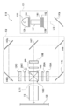
- It is a block diagram which shows the optical structure of a liquid crystal projector.
- liquid crystal display element 10 including an embodiment of the retardation plate of the present disclosure as a phase difference compensating element 20 will be described.
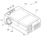
- the liquid crystal display element 10 is provided in, for example, a liquid crystal projector 110 (see FIGS. 39 and 40) described later.
- the liquid crystal display element 10 is a transmissive VA mode liquid crystal display element. That is, the liquid crystal layer of the liquid crystal display element 10 contains liquid crystal molecules that are oriented substantially perpendicular to the surface of the element in a no-voltage state. The liquid crystal display element 10 adjusts the voltage applied to the liquid crystal layer for each pixel to change the orientation of the liquid crystal molecules. As a result, the polarization state of the light transmitted through each pixel is controlled and an image is displayed.
- the liquid crystal display element 10 includes a polarizing element 15, a liquid crystal layer 17, and an analyzer 19 in this order from the light source side, and a phase difference compensating element 20 is provided between the liquid crystal layer 17 and the analyzer 19. Has been done.
- the polarizing element 15 is a polarizing plate that transmits only the polarized light component in the direction of the transmission axis T1 indicated by the arrow to the liquid crystal layer 17 side among the incident light. That is, the light incident on the liquid crystal layer 17 is only the incident light L0 in which the electric field vibrates in the direction parallel to the transmission axis T1.
- the analyzer 19 is a polarizing plate that transmits only the polarizing component in the direction of the transmission axis T2 indicated by the arrow among the light transmitted through the liquid crystal layer 17 and compensated for the phase difference by the phase difference compensating element 20.
- the detector 19 is arranged so that its transmission axis T2 is orthogonal to the direction of the transmission axis T1 of the polarizing element 15. That is, the analyzer 19 and the polarizing element 15 are arranged in a so-called cross Nicol. Therefore, the liquid crystal panel using the liquid crystal display element 10 is a normally black transmissive liquid crystal panel that displays black in a no-voltage state.
- the liquid crystal layer 17 is composed of transparent substrates 71 and 72 and rod-shaped liquid crystal molecules 75 enclosed between the transparent substrates 71 and 72.
- the transparent substrates 71 and 72 are composed of, for example, a glass substrate 77, a transparent electrode 78, an alignment film 79, and the like.
- the transparent substrate 71, the glass substrate 77, the transparent electrode 78, and the alignment film 79 are arranged in this order from the light source side.
- the alignment film 79, the transparent electrode 78, and the glass substrate 77 are arranged in order from the light source side.
- the transparent electrode 78 is connected to a TFT (Thin Film Transistor) circuit provided on the transparent substrate 71.
- This TFT circuit controls the orientation state of the liquid crystal molecules 75 by controlling the voltage between the transparent electrode 78 on the transparent substrate 71 and the transparent electrode 78 on the transparent substrate 72 which is a common electrode.
- the alignment film 79 is arranged so that the orientation direction thereof forms an angle of 45 degrees with the direction of the transmission axis T1 of the polarizing element 15.
- the liquid crystal molecules sandwiched between the pair of alignment films 79 are inclined and oriented according to the orientation direction of the alignment films 79.
- the liquid crystal molecule 75 is a rod-shaped liquid crystal molecule having negative dielectric anisotropy, and is oriented substantially perpendicular to the surface of the liquid crystal display element 10 in a no-voltage state. At this time, the liquid crystal molecules 75 do not substantially affect the phase of the light transmitted through the liquid crystal layer 17. That is, the light transmitted through the liquid crystal layer 17 in the non-voltage state passes through the liquid crystal layer 17 without changing its polarization direction.
- the information light L1 having substantially the same polarization direction as the incident light L0 is incident on the phase difference compensating element 20 from the liquid crystal layer 17. Since this information light L1 is light polarized in a direction perpendicular to the transmission axis T2 of the detector 19, it cannot pass through the detector 19. Therefore, by setting the pixels of the liquid crystal display element 10 to a non-voltage state, black color is displayed (hereinafter, dark display).
- the liquid crystal molecules 75 are tilted in the orientation direction of the alignment film 79. At this time, the liquid crystal molecule 75 changes the phase of the light transmitted through the liquid crystal layer 17 according to the inclination angle thereof. That is, the light transmitted through the liquid crystal layer 17 changes the polarization direction according to the inclination angle of the liquid crystal molecules 75.
- the polarizing component parallel to the transmission axis of the detector 19 transmits the detector 19. Therefore, by adjusting the pixels of the liquid crystal display element 10 to an appropriate voltage, the amount of light transmitted through the analyzer 19 is adjusted, and the intermediate gradation color is displayed.
- the phase difference compensating element 20 is provided between the liquid crystal layer 17 and the analyzer 19 as described above in order to compensate for the phase difference of the information light transmitted through the liquid crystal layer 17. Details of the phase difference compensating element 20 will be described later.
- the liquid crystal molecules 75 are oriented substantially perpendicular to the surface of the liquid crystal display element 10.
- the liquid crystal molecules 75 are intentionally tilted in advance by about 5 ° from the vertical direction even in a no-voltage state. This tilting arrangement is performed in order to suppress the occurrence of orientation defects of the liquid crystal molecules 75 called the reverse tilt domain.
- the reverse tilt domain is a disorder of the alignment state of the liquid crystal molecules 75 caused by the electric fields exerted between adjacent pixels.
- the Y2 axis and the Z2 axis are defined in a plane parallel to the surface of the liquid crystal display element 10, and the light transmitted through the liquid crystal layer 17 in the direction perpendicular to the surface of the liquid crystal display element 10.
- the X2 axis is defined with the traveling direction of light as positive in parallel with the light axis (transmitted light axis) L0. Further, the X2 axis and the Y2 axis are defined to be parallel to the transmission axes of the analyzer 19 and the polarizing element 15, respectively. Therefore, as shown in FIG. 2, the angle (azimuth) ⁇ formed by the tilt direction of the liquid crystal molecule 75 with the Y2 axis is 45 °.
- the angle formed by the liquid crystal molecule 75 with respect to the Y2-Z2 plane is the tilt angle ⁇ of the liquid crystal molecule 75.
- the tilt angle ⁇ changes in a range of about 0 ° or more and 85 ° or less depending on the magnitude of the voltage applied to each pixel.
- the tilt angle ⁇ is approximately 0 degrees, a sufficient voltage is applied to the liquid crystal layer 17, and the liquid crystal molecules 75 are oriented in parallel with the Y2-Z2 plane.
- the tilt angle ⁇ is 85 degrees, it is in a non-voltage state and the liquid crystal molecules 75 are oriented substantially perpendicular to the Y2-Z2 plane.
- the tilt angle ⁇ in this no-voltage state is the pre-tilt angle, and the liquid crystal molecule 75 is tilted about 5 ° with respect to the X2 axis, that is, the transmitted optical axis L0, along the orientation direction of the alignment film 79.
- phase advance axis F caused by the pre-tilt component of the liquid crystal molecules 75 in the liquid crystal layer 17 coincides with the pre-tilt direction.
- the phase-advancing axis F refers to an axis along an direction in which the refractive index is relatively low and the phase of light is relatively advanced in a medium that transmits light.
- the phase-advancing axis F due to the pretilt component of the liquid crystal molecule 75 in the liquid crystal layer 17 is simply referred to as the phase-advancing axis F of the liquid crystal layer 17.
- the phase difference compensating element 20 compensates for the phase difference of the information light transmitted through the liquid crystal layer 17 by generating a phase difference opposite to the phase difference generated in the liquid crystal display element 10. Therefore, the phase difference compensating element 20 is arranged so that the slow phase axis S of the phase difference compensating element 20 coincides with the phase advancing axis F due to the pretilt component of the liquid crystal layer 17.
- the slow-phase axis S which is the opposite of the phase-advance axis F, refers to an axis along an direction in which the refractive index is relatively high and the phase of light is relatively delayed in a medium that transmits light.
- the phase difference caused by the pretilt of the liquid crystal molecules 75 and the phase difference caused by the phase difference plate 21 are mutually arranged. Since the positive and negative directions are reversed, the phase difference caused by the pretilt of the liquid crystal molecule 75 can be compensated.
- phase difference plate 21 of the embodiment of the present disclosure can be applied.
- the retardation plate 21 of the first embodiment includes a glass substrate as an example of the substrate 23 and a retardation film 25 formed on one surface of the substrate 23.
- the retardation film 25 is an oblique film having a columnar structure 24 inclined with respect to the normal line N of the film forming surface 23a, which is one surface on which the retardation film 25 is formed.
- the retardation film 25 of this example is hereinafter referred to as an orthorhombic film 25.
- the orthorhombic film 25 is produced by depositing an inorganic material such as Ta 2 O 5 on the substrate 23 from an oblique direction by a so-called orthorhombic vapor deposition method. Specifically, as shown in FIG. 4, the vapor deposition source is held on the film forming surface 23a of the substrate 23 in a state where the film forming surface 23a of the substrate 23 is held in an inclined posture with respect to the vapor deposition source 27. The thin-film deposition material from 27 is obliquely incident and vapor-filmed.
- the columnar structure is inclined according to the incident direction (hereinafter, referred to as the vapor deposition direction) 28 of the vapor-film-deposited substance on the film-forming surface 23a.
- the body 24 grows to form an oblique film 25 having a structure in which the columnar structure 24 stands.
- the angle formed by the vapor deposition direction 28 and the normal line N of the film forming surface 23a is referred to as the vapor deposition angle ⁇ .
- the substrate 23 is installed at an angle formed by the horizontal plane (a surface parallel to the horizontal floor surface) shown by the dotted line in FIG. 4 and the film forming surface 23a. It is called the angle ⁇ . That is, the installation angle ⁇ when the substrate 23 is installed horizontally is 0 °, and the installation angle ⁇ when the substrate 23 is installed perpendicular to the horizontal is 90 °.
- the longitudinal direction 29, which is the growth direction of the columnar structure 24 of the oblique film 25, generally does not match the vapor deposition direction 28 (see also FIG. 4), but the columnar structure 24 forms the film of the substrate 23.
- the growth angle ⁇ formed by the normal line N of the surface 23a has a positive correlation with the vapor deposition angle ⁇ . That is, when the vapor deposition angle ⁇ is large, the growth angle ⁇ of the columnar structure is large, and when the vapor deposition angle ⁇ is small, the growth angle ⁇ of the columnar structure is also small.
- the growth direction 29 of the columnar structure 24 tends to rise from the film forming surface 23a rather than the vapor deposition direction 28, and the growth angle ⁇ is smaller than the vapor deposition angle ⁇ ( ⁇ ⁇ ). Due to the columnar structure in which the columnar structure 24 stands, the retardation film 25 exhibits refractive index anisotropy as an optical characteristic and functions as an O plate.
- the growth direction 29 of the columnar structure 24 is the longitudinal direction of the columnar structure 24.
- the growth direction 29 is referred to as a longitudinal direction 29.
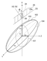
- the refractive index anisotropy of the oblique film 25 is conceptually represented by a refractive index ellipsoid 102 having three main refractive indexes nx, ny, and nz as axes.
- 6A is a view of the refractive index ellipsoid 102 viewed from the Y-axis direction in FIG. 5
- FIG. 6B is a view of the refractive index ellipsoid 102 viewed from the Z-axis direction in FIG.
- FIG. 6C is a view of the refractive index ellipsoid 102 as viewed from the X-axis direction in the figure.
- the main refractive index is the long axis of the refractive index of the refractive index ellipse and the length of the ellipse obtained by cutting the refractive index ellipse along the major axis. It means the refractive index in the direction of the first minor axis perpendicular to the axis and the refractive index in the direction of the second minor axis perpendicular to the major axis and the first minor axis.
- one of the three main refractive indexes nx, ny, and nz of the refractive index ellipsoid 102 forms an axis that coincides with the longitudinal direction 29 of the columnar structure 24.
- the axis corresponding to the longitudinal direction 29 of the columnar structure 24 is defined as the X axis
- the main refractive index along the X axis is defined as nx.
- the major axis direction of the ellipsoid 104 passing through the center C of the refractive index ellipsoid 102 and perpendicular to the X axis is defined as the Y axis
- the minor axis direction is defined as the Z axis.
- the main refractive index in the Y-axis direction is ny
- the main refractive index in the Z-axis direction is nz.
- the three main refractive indexes nx, ny, and nz satisfy the following conditional expression (1). ny>nx> nz (1)
- FIG. 7A shows the relationship between each axis of the refractive index ellipsoid 102 with respect to the film surface of the retardation plate 21 perpendicular to the incident direction of light with respect to the retardation plate 21 and the incident direction of light.
- the normal line N of the film forming surface 23a of the substrate 23 is set as the XS axis
- the YS axis and the ZS axis are set on the film forming surface 23a perpendicular to the XS axis.
- the axis obtained by projecting the Y axis of the refractive index ellipsoid 102 onto the film forming surface 23a is defined as the YS axis, and the direction orthogonal to the YS axis is defined as the ZS axis.
- the X-axis of the refractive index ellipsoid 102 is in the XS-ZS plane and is ⁇ -inclined from the XS axis.
- the ZS axis coincides with the axis obtained by projecting the X axis onto the film forming surface 23a.
- the refractive ellipsoid 102 When the refractive ellipsoid 102 is cut in a plane passing through the center C of the refractive ellipsoid 102 and parallel to the film forming surface 23a, its cross section corresponds to the major axis radius in the YS axis direction as shown in FIG. 7B.
- the ellipsoid 106 has a refraction factor nys and a refraction factor nzs corresponding to the minor axis radius in the ZS axis direction.
- the oblique film 25 exhibits birefringence having a refractive index of nys in the YS axis direction and a refractive index of nzs in the ZS axis direction with respect to light incident along the XS axis.
- This refractive index nys is larger than the refractive index nzs. That is, the retardation film 25 has a slow phase axis S1 in the YS axis direction, which has the maximum refractive index with respect to light incident from the XS axis direction.
- the retardation film 25 has a phase advance axis F1 in the ZS axis direction, which has a minimum refractive index with respect to light incident from the XS axis direction.
- the slow-phase axis S1 is orthogonal to the axis (ZS axis) obtained by projecting the X-axis corresponding to the growth direction 29 onto the film forming surface 23a. That is, it is the YS axis in which the Y axis corresponding to the maximum main refractive index ny of the three main refractive indexes ny is projected onto the film forming surface 23a, and the incident light corresponds to the main refractive index ny.
- the slow phase axis S1 is orthogonal to the ZS axis.
- FIG. 8A is a view of an ellipsoid 107 having a cross section cut along an XS-ZS plane passing through the center C of the ellipsoidal index 102 as viewed from the YS axis direction.
- FIG. 8B is a view of an ellipsoid 106 having a cross section obtained by cutting the refractive index ellipsoid 102 in the YS-ZS plane passing through the center C from the XS axis direction.
- FIG. 8C is a view of an ellipsoid 108 having a cross section obtained by cutting the refractive index ellipsoid 102 in the XS-YS plane passing through the center C from the ZS axis.
- the X-axis and Z-axis of the refractive index ellipsoid 102 showing the refractive index anisotropy of the retardation film 25 are rotated by ⁇ about the YS axis with respect to the XS-axis and ZS-axis of the retardation plate. There is.
- phase difference generated in the incident light changes depending on the inclination of the light incident on the refractive index ellipsoid 102.
- the phase difference that occurs in the refractive index ellipsoid 102 is a cross section perpendicular to the incident light, and depends on the difference between the major axis and the minor axis of the ellipse formed in the cross section that passes through the center C of the refractive index ellipsoid 102.
- the incident angle in the direction of tilting the columnar structure 24 toward the growth direction 29 with respect to the XS axis which is the normal line N of the oblique film 25 is positive (+ ⁇ )
- the columnar structure 24 Let the incident angle in the tilting direction be negative (- ⁇ ) on the side opposite to the growing direction.
- the phase difference Re (0) with respect to the light incident on the oblique film 25 along the XS axis, that is, the light incident at an incident angle of 0 ° is referred to as a front phase difference.
- the refractive index nys in the YS axis direction which is the long axis of the ellipse of the refractive index ellipse on the plane perpendicular to the XS axis, that is, the YS-ZS plane (see FIG. 8B).
- the oblique film 25 of the present embodiment has a ratio of the phase difference Re (+30) of the incident light having a negative incident angle of +30 ° and the phase difference Re (-30) of the incident light having a positive incident angle of ⁇ 30 °.
- the Re (30) ratio of a certain phase difference ratio satisfies the following conditional expression (2).
- the retardation plate 21 provided with the oblique film 25 as described above is such that the slow axis S1 of the oblique film 25 and the tilt direction of the liquid crystal molecules 75 are parallel to each other, that is, the liquid crystal. It is arranged so as to be parallel to the phase advance axis F due to the pretilt of the molecule 75.
- the retardation plate 21 is used as the phase difference compensating element 20
- the slow phase axis S1 of the oblique film 25 corresponds to the slow phase axis S in the phase difference compensating element 20.
- the phase difference caused by the pretilt of the liquid crystal molecule 75 and the phase difference caused by the retardation plate 21 are opposite to each other, so that the phase difference can be compensated.
- the pre-tilted liquid crystal molecules 75 are the cause of causing the phase difference, but also the diffraction of light, the polarizing element 15 and the analyzer due to the fine structure of the liquid crystal cell.
- the phase difference is caused by various factors such as the generation of the phase difference due to 19. Therefore, the retardation plate 21 may not always have the best arrangement in which the slow phase axis S1 and the phase advance axis F of the liquid crystal molecule coincide with each other.
- the azimuth angle at which high contrast can be obtained while observing the contrast of the projected image is rotationally adjusted around the XS axis so as to be.
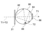
- the haze of the orthorhombic membrane 25 can be measured using an integrating sphere.
- the integrating sphere 80 includes an incident opening 82 and an exit opening 84 provided at a position facing the incident opening 82 and rotated by 180 ° from the incident opening 82.
- the photodetectors 86 and 88 are provided inside the exit opening 84 of the integrating sphere 80 and the integrating sphere 80, respectively.
- the photodetector 86 provided in the exit opening 84 receives the light that has traveled straight through the integrating sphere among the light incident along the diameter of the integrating sphere 80 from the incident opening 82.
- the photodetector 88 arranged in the integrating sphere 80 does not go straight among the incident light, but receives the scattered light reflected in the integrating sphere 80.
- the retardation plate 21 is arranged in the incident opening 82 so that the film surface is perpendicular to the light incident along the diameter.
- the incident light L is vertically incident on the film surface of the retardation plate 21, passes through the retardation plate 21, travels straight without being scattered by the retardation plate 21, and the photodetector measures the amount of vertically transmitted light T1 that reaches the exit aperture. Detect at 86.
- the photodetector 88 arranged in the integrating sphere detects the scattered light amount T2 that is scattered by the retardation plate 21 of the incident light L and repeatedly reflected in the integrating sphere 80 without going straight.
- the haze of the orthorhombic film 25 is obtained by measuring the haze of the substrate 23 alone by the above means and subtracting the haze of the substrate only from the haze of the retardation plate 21. When the substrate 23 is a glass substrate, the haze is almost zero.
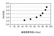
- the present inventor has a Re (30) ratio and a haze in an oblique film 25 having a refractive index anisotropy represented by a refractive index ellipsoid 102 in which the main refractive indexes nx, ny, and nz satisfy the above equation (1). It was found that there is a correlation with and as shown in FIG. When the Re (+30), Re (-30) and Re (30) ratios satisfy the above (2), the haze of the orthorhombic membrane 25 can be suppressed to 0.1% or less. By setting the Re (30) ratio to 4.0 or less, that is, by suppressing the haze to 0.1% or less, the Re (30) ratio is applied to the liquid crystal display element as the phase difference compensating element 20. The contrast can be improved as compared with the case where is more than 4.0.
- the orthorhombic film 25 satisfying the above equations (1) and (2) can be manufactured by adjusting the substrate installation angle ⁇ at the time of orthorhombic vapor deposition.
- a plurality of oblique films are produced by changing the substrate installation angle ⁇ with the vapor deposition source 27 placed directly under the center of the substrate 23, and the Re (30) ratio is set.
- the relationship shown in FIG. 12 was obtained.
- tantalum pentoxide (Ta 2 O 5 ) is used as the material of the orthorhombic membrane 25.
- the Re (30) ratio increases as the substrate installation angle ⁇ increases.
- a Re (30) ratio of 4.0 or less can be obtained by setting the substrate installation angle ⁇ to approximately 85 degrees or less.
- the relationship between the substrate installation angle ⁇ and the Re (30) ratio depends on the configuration of the vapor deposition apparatus, and the relationship between the Re (30) ratio and the substrate installation angle ⁇ shown in FIG. 12 changes depending on the vapor deposition apparatus.
- the tendency that the Re (30) ratio increases as the substrate installation angle ⁇ increases is common regardless of the configuration of the vapor deposition apparatus. Therefore, if the relationship between the two is measured in advance, the orthorhombic membrane 25 having a desired Re (30) ratio can be obtained.
- the Re (30) ratio preferably satisfies the following conditional expression (2-1).
- this conditional expression (2-1) the effect of improving the black display unevenness can be obtained in the retardation plate 31 (see FIG. 16) provided with two layers of the orthorhombic film 25, which will be described later.
- Re (30) ratio satisfies the following conditional expression (2-2).
- Re (30) ratio satisfies the following conditional expression (2-3).
- the material of the orthorhombic film 25 an oxide containing at least one of Si, Nb, Zr, Ti, La, Al, Hf and Ta can be used. That is, the orthorhombic film 25 can be composed of an oxide containing at least one of Si, Nb, Zr, Ti, La, Al, Hf and Ta. By using these materials, an orthorhombic membrane composed of a good columnar structure can be obtained.
- the method of forming the oblique film 25 is not limited to the above method. Any method may be used as long as the columnar structure 24 can be grown on the film forming surface 23a of the substrate 23 in the direction inclined from the normal line N to obtain the oblique film 25.
- the vapor deposition method is not limited to vacuum vapor deposition, and electron beam vapor deposition, ion plating, or the like can be used. Further, chemical vapor deposition (CVD) may be used. Further, a sputtering method, a reactive sputtering method and the like can also be used.
- the incident angle dependence of the retardation was as shown in FIG. 13
- the plane orthogonal to the incident light is considered in the refractive index ellipsoid 102.
- the YS-ZS plane is a plane orthogonal to the incident light in the refractive index ellipsoid 102 with respect to the light incident from the XS axis direction.
- the ZY plane is orthogonal to the light LX incident from the X-axis direction.
- the refractive index n ( ⁇ ) in the axial direction changes depending on the incident angle ⁇ .
- the phase difference with respect to the incident light passes through the center C of the refractive ellipsoid 102 and is proportional to the difference between the major axis radius and the minor axis radius of the ellipsoid of the refractive index ellipsoid 102 on the plane orthogonal to the incident light.
- the phase difference was measured by subtracting the refractive index n ( ⁇ ), which changes depending on the incident angle, from the reference refractive index nys with the refractive index nys as a reference.
- the phase difference increases as the incident angle ⁇ increases in the positive direction, and the phase difference becomes almost constant when the incident angle ⁇ is 30 ° or more.
- the phase difference decreases, and the incident angle ⁇ is 50 ° and the phase difference is 0.
- d2 d / cos ( ⁇ -90).
- a screen was placed at a position where light passing through the analyzer 19 was projected, white display and black display were performed on the screen, and contrast and black display unevenness were evaluated according to the following criteria, respectively.
- the slow axis of the orthorhombic film was aligned with the phase advance axis F caused by the pretilt component of the liquid crystal layer 17.
- the phase-advancing axis due to the pre-tilt component of the liquid crystal layer 17 in this example has a 45 ° azimuth, and the slow-phase axis S of the oblique film of the retardation plate is aligned with the 45 ° azimuth.
- the value of the illuminance at the time of white display when the illuminance of black display was set to 1 was measured, and the measured value was evaluated as follows.
- the black display: white display was 800: 1 when the phase difference compensating element 20 was not provided.
- Black display unevenness ((A + D)-(B + C)) / E Calculated as.
- the calculated value of black display unevenness was evaluated as follows. A: 2 or less B: 2 or more, 4 or less C: 4 or more, 6 or less D: 6 or more
- the A evaluation was 7 points
- the B evaluation was 5 points
- the C evaluation was 3 points
- the D evaluation was 0 points.
- the total score was obtained by adding the scores of display unevenness. The higher the total score, the better the quality of the retardation plate. The results are shown in Table 1 below.
- Samples 1-2 to 1-8 in which Re (30) shown in Table 1 is 1.1 to 4 correspond to the embodiment of the retardation plate of the present disclosure.
- the samples 1-2 to 1-8 have a higher contrast evaluation than the other samples, and the high contrast is improved.
- the total score of the contrast and the black display unevenness is high, and the effect of suppressing the black display unevenness is obtained while improving the contrast.
- the samples with Re (30) of 1.1 to 2.0 the effects of further improving the contrast and suppressing the black display unevenness are obtained.
- Phase difference plate of the second embodiment The retardation plate used as the phase difference compensating element 20 is not limited to the configuration in which only one oblique film 25 is provided as in the above retardation plate 21, but two or more oblique films 25 are laminated and provided. You may.
- the retardation plate of the second embodiment the retardation plate 31 provided with two layers of oblique films will be described.
- the retardation plate 31 of the present embodiment is provided with a first oblique film 25a on one surface of the substrate 23, and a second oblique film 25b is formed on the other surface. .. That is, in the retardation plate 31, the orthorhombic film is formed layer by layer on both sides of the substrate.
- the first orthorhombic film 25a and the second orthorhombic film 25b in the present embodiment are manufactured in the same manner as the above-mentioned orthorhombic film 25, and their optical properties and the like are also the same. That is, the first orthorhombic film 25a and the second orthorhombic film 25b are represented by a refractive index elliptical body 102 in which the main refractive indexes nx, ny, and nz satisfy the above equation (1), similarly to the oblique film 25. Has a refractive index anisotropy. Further, the Re (+30), Re (-30) and Re (30) ratios satisfy the above equation (2).
- the haze can be suppressed to 0.1% or less, respectively.
- the haze is integrated, so that the haze as the retardation plate 31 increases.
- the orthorhombic films 25a and 25b satisfy the above equations (1) and (2), the haze when laminated can be suppressed, and the haze when laminated can be reduced to 0.3% or less. (See FIG. 28 below).
- the retardation plate has a haze of 0.3% or less when two or more layers of oblique films 25a and 25b are provided, Re (30) is applied to the liquid crystal display element as the phase difference compensation element 20.
- the contrast can be improved and the black display unevenness can be suppressed as compared with the case where the ratio exceeds 4.
- the slow axis S21 of the first oblique film 25a and the slow axis S22 of the second oblique film 25b intersect at an intersection angle of 90 ° ⁇ 3 °, which is substantially orthogonal to each other.
- the first orthorhombic film 25a and the second orthorhombic film 25b are arranged therein.
- the slow axis S1 of the oblique film 25 and the phase advance axis F of the liquid crystal layer 17 are parallel to each other in the liquid crystal display element 10. It is arranged so that it becomes.
- the retardation plate 31 provided with the two layers of the oblique films 25a and 25b the slow axis S21 of the first oblique film 25a and the slow axis S22 of the second oblique film 25b are synthesized.
- the synthetic slow-phase axis S2 is arranged so as to be parallel to the phase-advancing axis F of the liquid crystal layer 17.
- the slow phase axis S21 of the first oblique film 25a is in the 90 ° direction. They are aligned and the slow axis S22 of the second oblique film 25b is arranged so as to coincide with the 0 ° direction.
- the combined slow-phase axis S2 which is a combination of the slow-phase axis S21 and the slow-phase axis S22, has a 45 ° direction and coincides with the phase-advancing axis F.
- the intersection angle of the slow axis of the first orthorhombic membrane 25a and the second orthorhombic membrane 25b will be examined. According to the studies by the present inventors, it is preferable that the crossing angle deviates slightly from 90 °. It is preferably deviated in the range of ⁇ 5 ° with respect to 90 °, and more preferably deviated in the range of ⁇ 3 °. The reason will be explained below.
- the in-plane optical anisotropy of the orthorhombic film 25 will be described with reference to FIG.
- the axis obtained by projecting the vapor deposition direction 28 (see FIGS. 3 and 4) onto the film forming surface 23a (see FIG. 3) is orthogonal to the slow phase axis S1.
- the axis in which the vapor deposition direction 28 is projected onto the film forming surface 23a and the axis in which the growth direction 29 is projected on the film forming surface 23a coincide with each other.
- the phase advance axis F1 orthogonal to the slow phase axis S1 is defined as an orientation of 0 ° ⁇ 180 °.
- FIG. 18B is a cross section of the orthorhombic membrane 25 shown in FIG. 18A along the phase advance axis F1
- FIG. 18C is a cross section of the orthorhombic membrane 25 shown in FIG. 18A along the slow axis S1.
- the columnar structure 24 is inclined in a cross section along the phase advance axis F1. Therefore, even if the incident angle ⁇ is the same, if the incident direction is different, the phase difference that the light receives when passing through the columnar structure 24 is different.
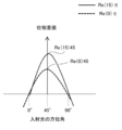
- the phase difference between the incident angle ⁇ and the azimuth angle ⁇ may be referred to as Re ( ⁇ ) ⁇ .
- the phase difference at an incident angle of 15 ° and an azimuth angle of 90 ° is Re (15) 90 °.
- phase difference Re ( ⁇ ) with respect to the incident light at the incident angle ⁇ inclined in the growth direction from the normal line described in FIG. 9 is Re ( ⁇ ) 180 according to this notation, which is the growth direction from the normal line.
- the phase difference Re ( ⁇ ) with respect to the incident light having an incident angle ⁇ tilted to the opposite side is Re ( ⁇ ) 0.
- the orientation of the liquid crystal display element 10 of this example is described in a single-layer oblique film in which the phase-advancing axis due to the pretilt of the liquid crystal molecules 75 of the liquid crystal layer 17 is defined as a 45 ° orientation. It is different from the above orientation.
- the orientation of the retardation plate 31 follows the orientation of the liquid crystal display element 10.
- the combined slow axis S21 of the first oblique film 25a and the second oblique film 25b and the combined slow axis S2 of S22 are oriented at 45 °. It is installed so that it becomes.
- the phase difference Re ( ⁇ ) between the first orthorhombic film 25a and the second orthorhombic film 25b has azimuth dependence, respectively.
- the phase difference Re ( ⁇ ) of the retardation plate 31 in which both are laminated is the sum of the phase differences between the first oblique film 25a and the second oblique film 25b.
- the liquid crystal layer 17 has a front phase difference component due to the pretilt component in the 45 ° direction, has a peak in the 45 ° direction, and exhibits a substantially symmetrical azimuth angle dependence in the range of ⁇ 45 °.
- the Re (0) 45 of the retardation plate 31 is zero, so that the liquid crystal layer 17 The front phase difference of is not compensated.
- the range of 45 ° azimuth ⁇ 45 ° in the retardation plate 31 That is, the azimuth dependence of the phase differences Re (0) and Re (15) in the 0 ° to 90 ° directions is schematically shown in FIG.
- the front phase difference Re (0) of the phase difference plate 31 shows an azimuth angle dependence having a peak in the 45 ° direction.
- the front phase difference Re (0) in the 45 ° direction is generated by about 0.1 nm to 5 nm so that the phase difference is about the same as the front phase difference in the phase-advancing axis direction of the liquid crystal layer 17. This makes it possible to satisfactorily compensate for the front phase difference of the liquid crystal layer in the 45 ° direction. That is, as the retardation plate 31, it is preferable that the front phase difference Re (0) in the slow phase axial direction is 0.1 nm to 5 nm.
- the retardation plate 31 provided by laminating the first and second two layers of the oblique films 25a and 25b has the crossing angle of the slow axis of each of the two layers of the oblique films 25a and 25b and the 45 ° direction.
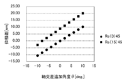
- the relationship between Re (0) 45 and Re (15) 45 of the retardation plate in FIG. 21 is as shown in FIG. 21 as an example.
- the case where the slow phase axes are orthogonal to each other is defined as 0 °
- the case where the crossing angle is larger than 90 ° is positive
- the crossing angle is smaller than 90 ° is negative.
- phase difference Re (0) of the phase difference plate 31 in the range of zero to ⁇ 10 nm by changing the slow phase axis by ⁇ 10 ° from the orthogonal state.
- phase difference Re (15) of the phase difference plate 31 also changes in the range of ⁇ 10 nm from the value (9 nm) in the orthogonal state.
- the crossing angle of the slow axes of the two layers of the oblique films 25a and 25b to be laminated may be set according to the front phase difference Re (0) of the liquid crystal layer 17 in the 45 ° direction of the liquid crystal display element 10 to be applied.
- the deviation of the crossing angle between the slow axes of the first orthorhombic film 25a and the second orthorhombic film 25b from 90 ° may be within ⁇ 5 °. It is preferably within ⁇ 3 °, and more preferably within ⁇ 3 °.
- the liquid crystal layer 17 has a front phase difference component due to the pretilt component in the 45 ° direction, has a peak in the 45 ° direction, and exhibits a substantially symmetrical azimuth angle dependence in the range of ⁇ 45 °.
- the phase difference Re ( ⁇ ) when incident at another incident angle ⁇ also has a peak in the 45 ° azimuth, and is dependent on a substantially symmetrical azimuth in the range of ⁇ 45 °. Show sex.
- the phase difference Re ( ⁇ ) of the retardation plate 31 is substantially symmetric with respect to the direction 45 ° in the range of 45 ° direction ⁇ 45 °.
- the difference between the phase difference Re (15) 90 in the 90 ° direction, which is 45 ° direction + 45 °, and the phase difference Re (15) 0 in the 0 ° direction, which is 45 ° direction ⁇ 45 °, is an index of symmetry. The smaller the difference, the higher the symmetry with respect to the direction of 45 °.
- the phase difference between the phase difference Re (15) 90 and the phase difference Re (15) 0 is preferably within ⁇ 6 nm.
- the phase difference Re ( ⁇ ) of the phase difference plate 31 shows a positive maximum peak in one direction of the combined slow phase axis S2.
- the orientation of the combined slow phase axis showing the maximum peak is arranged so as to coincide with the phase advance axis F of the liquid crystal layer 17.
- the retardation plate 31 has an azimuth angle at which the phase difference Re (15) generated with respect to the incident light having an incident angle of + 15 ° with respect to the normal line is maximized in the azimuth angle from 0 ° to 360 °. Is the reference azimuth angle ⁇ a.
- the retardation plate 31 is arranged so that the reference azimuth angle ⁇ a is 45 °. That is, the retardation plate 31 has the first phase difference Re (15) ⁇ a + 45 of the incident light when the azimuth is + 45 ° with respect to the reference azimuth angle ⁇ a, and the azimuth is ⁇ 45 ° with respect to the reference azimuth angle ⁇ a.
- the absolute value of the difference between the incident light and the second phase difference Re (15) ⁇ a-45 is preferably 6 nm or less.
- the difference between the phase difference Re (15) ⁇ a + 45 in the ⁇ a + 45 ° direction and the phase difference IRe (15) ⁇ a-45 in the ⁇ a-45 ° direction centered on the azimuth angle ⁇ a where the phase difference Re (15) is maximum is ⁇ 6 nm.
- the retardation plate 31 has high symmetry in the azimuth angle range of ⁇ a ⁇ 45 ° with the azimuth angle ⁇ a as the center. If the phase difference plate 31 has high symmetry in the azimuth angle range of ⁇ a ⁇ 45 ° with respect to the azimuth angle ⁇ a, then ⁇ 45 ° with respect to the azimuth of the phase advance axis of the liquid crystal layer having azimuth dependence.
- phase difference plate having a phase difference of opposite phases can be realized over a range.
- the phase difference in the range of the pretilt direction ⁇ 45 ° is the largest. Therefore, if the phase difference plate 31 shows the phase difference of the opposite phase over this range, the phase difference of the liquid crystal layer 17 can be obtained. It can be effectively compensated. Therefore, when such a phase difference plate 31 is applied as the phase difference compensating element 20 of the liquid crystal display element 10, the contrast can be effectively improved and black display unevenness can be suppressed.
- the refractive index anisotropy of both may not be completely the same.
- the difference ⁇ Re (0) of the front phase difference Re (0) between the first oblique film 25a and the second oblique film 25b is 3 nm or less.
- the orientation (peak orientation) at which the IRe (15) of the retardation plate 31 is maximum has a relationship as shown in FIG. 22 as an example.
- I is the phase difference of the retardation plate 31, and is added to distinguish it from the phase difference of each of the orthorhombic films 25a and 25b.
- FIG. 22 shows the results of investigating the relationship between ⁇ Re (0) and IRe (15) peak orientation.
- ⁇ Re (0) when ⁇ Re (0) is zero, the IRe (15) peak direction coincides with the 45 ° direction, which is the phase advance axis direction due to the pretilt component of the liquid crystal layer 17.
- ⁇ Re (0) when ⁇ Re (0) is smaller than zero, the IRe (15) peak direction becomes large, and when ⁇ Re (0) becomes larger than zero, the IRe (15) peak direction becomes small.
- the efficiency of phase difference compensation may decrease due to the deviation of the IRe (15) peak direction from the 45 ° direction.
- ⁇ Re (0) and the peak value IRe (15) max of the phase difference IRe (15) of the phase difference plate 31 in the 0-360 ° direction have a relationship as shown in FIG. 23.
- IRe (15) max is the smallest at about 9 nm when ⁇ Re (0) is zero.
- IRe (15) max increases. In this case, overcompensation of the phase difference may occur, and the efficiency of the phase difference compensation may decrease.
- ⁇ IRE (0) and ⁇ IRE (15) which is the difference between ⁇ Re (0) and IRe (15) at the orientation ⁇ 45 ° of the combined slow axis S2 in the retardation plate 31, that is, the difference between IRe (15) 90-IRE (15) 0. It has a relationship as shown in FIG. 24 with 15).
- ⁇ IRE (15) is close to 0 means that the symmetry in the range of ⁇ 45 ° is high around the direction of the synthetic slow phase axis S2.
- a large phase difference occurs in the range of ⁇ 45 ° in the direction of the phase advance axis F due to the pretilt component.
- phase difference generated in the liquid crystal layer 17 is symmetrical in the range of ⁇ 45 ° with respect to the direction of the phase advance axis F. Therefore, it is considered that the higher the symmetry of the phase difference plate 31 in the range of ⁇ 45 ° with respect to the direction of the combined slow phase axis S2, the higher the efficiency of the phase difference compensation.
- the IRe (15) peak direction is in the vicinity of the 45 ° direction, and the symmetry is high in the range of the 45 ° direction ⁇ 45 °. Is preferable. Therefore, the ⁇ Re (0) of the frontal phase difference between the two layers of the oblique films 25a and 25b is preferably within ⁇ 3 nm, preferably within ⁇ 1 nm, and the difference in the frontal retardation is 0. Most preferred.
- FIGS. 25 to 32 An example of design change for a retardation plate provided with two layers of oblique films will be described with reference to FIGS. 25 to 32.
- FIGS. 16 and 25 to 32 the same elements are designated by the same reference numerals.
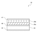
- antireflection films 41 and 42 are provided on both sides of the substrate 23, and a first oblique plate which is the outermost surface of the retardation plate 31 is provided. It is preferable to provide the antireflection films 43 and 44 on one surface of the square film 25a and one surface of the second oblique film 25a, respectively. By providing the antireflection films 41, 42, 43, 44, it is possible to suppress the reflection of the incident light at each interface, increase the transmittance, and further enhance the haze suppressing effect.
- the retardation plate 31 of the second embodiment is provided with the first oblique film 25a on one surface of the substrate 23 and the second oblique film 25b on the other surface.
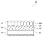
- two layers of orthorhombic films 25a and 25b may be formed on one side of the substrate 23 as in the retardation plate 32 shown in FIG. 26.
- the orthorhombic films 25a and 25b are provided on both sides of the substrate 23, respectively, the scattering at the interface caused when the orthorhombic films 25a and 25b are directly laminated can be suppressed. It is possible, and as a result, haze can be suppressed, which is preferable.
- both sides of the substrate 23 and the second oblique film 25b which is the outermost surface of the retardation plate 32 are formed. It is preferable that the antireflection films 45, 46, and 47 are provided on one surface, respectively. By providing the antireflection films 45, 46, and 47, it is possible to suppress the reflection of incident light at the interface, increase the transmittance, and further enhance the haze suppressing effect.
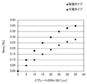
- FIG. 12 shows the relationship between the haze and the substrate installation angle ⁇ .
- the second oblique film 25b is formed in a state where the substrate is rotated by approximately 90 °, and the first oblique film 25b is formed.
- the slow axes S21 and S22 of the orthorhombic membrane and the second orthorhombic membrane are substantially orthogonal to each other (see FIGS. 16 and 26). Further, both sides of the substrate and the outermost surface of the retardation plate are provided with any of the antireflection films 41 to 47 (see FIGS. 25 and 27).
- the numerical values shown in parentheses are the Re (30) ratios for the single membrane orthorhombic membrane 25. As shown in FIG. 28, when the Re (30) ratio is 4 or less, the haze can be suppressed to about 0.3% or less. Further, from FIG. 28, the retardation plate 31 formed by distributing the orthorhombic films 25a and 25b to both sides of the substrate is compared with the retardation plate 32 in which two layers are laminated on one side, whichever Re (30) is used. Even in the ratio, the haze is kept low.
- the haze can be suppressed to about 0.2% or less if the Re (30) ratio is 4 or less.
- the two layers of the orthorhombic films 25a and 25b are directly contacted and laminated, and the two layers of the orthorhombic films 25a and 25b are laminated. It is considered that the effect of suppressing the scattering generated at the interface of the above is shown.
- the retardation plate 32 provided by laminating two layers of the oblique films 25a and 25b on one surface, as shown in FIG. 29, the first oblique film 25a and the second oblique film 25b are provided. It is preferable to provide a flattening layer 26 in between.
- the flattening layer 26 is an example of an intermediate layer.
- the flattening layer 26 has a function of flattening fine irregularities generated on the surface of the first oblique film 25a formed earlier.
- the flattening layer 26 not only the silicon oxide film (SiO 2 ) but also a metal oxide such as tantalum pentoxide (Ta 2 O 5 ) or magnesium fluoride (Mg F 2 ) can be used.
- the flattening layer 26 is formed, for example, by arranging a vapor deposition source directly under the substrate and performing front vapor deposition instead of oblique vapor deposition.
- the flattening layer 26 between the first orthorhombic film 25a and the second orthorhombic film 25b By providing the flattening layer 26 between the first orthorhombic film 25a and the second orthorhombic film 25b, the fine irregularities on the surface of the first orthorhombic film 25a are flattened, and the second The orthorhombic film 25b can be formed into a flat surface.
- the flattening layer 26 on the surface of the first oblique film 25a and reducing the surface roughness of the film forming surface of the second oblique film 25b, scattering at the interface is suppressed. Therefore, the haze in the retardation plate 32 can be suppressed. Further, as compared with the case where the second oblique film 25b is directly formed on the first oblique film 25a, the effect of improving black display unevenness and contrast is high.
- FIG. 30 shows the relationship between the haze and the substrate installation angle ⁇ for the retardation plate 32 (see FIG. 29) in which the flattening layer 26 having a silicon oxide film of 15 nm is provided between the orthorhombic films 25a and 25b.
- the data for the retardation plate 32 provided with the flattening layer 26 is indicated by a black triangular marker.
- FIG. 30 shows the data shown in FIG. 28 at the same time for comparison.
- the retardation plate 31 provided with the flattening layer 26 between the orthorhombic films 25a and 25b has the orthorhombic films 25a and 25b. It is possible to significantly reduce the haze as compared with the retardation plate 32 which is laminated by contacting the two.
- the Re (30) ratio is 4 or less, the haze can be suppressed to approximately 0.25% or less.
- the suitable film thickness of the flattening layer 26 was examined as follows.
- SiO 2 , Ta 2 O 3 or Mg F 2 was used as the flattening layer 26, and samples were prepared in which the film thickness was changed from 5 nm to 30 nm, respectively.
- an orthorhombic membrane having a Re (30) ratio of 2.0 was used.
- the refractive index is a value for a wavelength of 400 nm.
- the thickness of the flattening layer 26 is preferably such that the optical path length is about 40 nm, that is, about 1/10 or less with respect to the wavelength of 400 nm. Further, by setting the physical film thickness to 10 nm or more, the effect of flattening the film surface of the orthorhombic film and suppressing scattering can be enhanced.
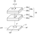
- a phase plate having two substrates on which the two orthorhombic films are formed may be used.
- the retardation plate 35 may be formed by stacking the retardation plates 35b.
- the embodiment in which two or more orthorhombic films are laminated is not only the embodiment in which a plurality of orthorhombic films 25a and 25b are laminated on one substrate 23, but also different substrates 22a.
- the present invention includes an embodiment in which the orthorhombic films 25a and 25b formed on the 22b are superposed on the optical path.
- the rotation angles of the phase advancing axes S31 and S32 are rotated by rotating one to the center of the XS axis at the time of assembly according to the liquid crystal display element 10 to be applied. Can be changed.
- the phase difference Re (0) and Re (15) of the liquid crystal layer 17 having manufacturing variations can be individually compensated for the phase difference most efficiently, that is, the contrast performance is maximized. It becomes possible to correspond to.
- the liquid crystal display element 10 provided with the liquid crystal layer 17 and the phase difference compensating element 20, at least one of the plurality of substrates 22a and 22b on which at least one retardation film is formed is formed.
- the contrast of the liquid crystal display element 10 can be adjusted by rotating the liquid crystal display element 10 with respect to the other substrate 22a about the XS axis perpendicular to the surface.
- the retardation plate of the present disclosure may have three or more layers of the orthorhombic film 25 laminated.
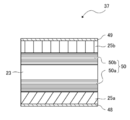
- a retardation plate 36 having the orthorhombic films 25a and 25b on one surface of the substrate 23 and the orthorhombic films 25c on the other surface is used as the retardation compensating element 20. You can also do it.
- the retardation plate 36 is provided with antireflection films 41, 42, 43, 44 on both sides of the substrate 23 and on the outermost surface of the retardation plate 36, respectively.
- the slow axis S21 of the first oblique film 25a In the case of the retardation plate 36 in which the oblique film 25 has three layers, the slow axis S21 of the first oblique film 25a, the slow axis S22 of the second oblique film 25b, and the third oblique film 25c.
- the slow phase axis S3 formed by synthesizing the slow phase axis S23 is arranged so as to be parallel to the phase advance axis F of the liquid crystal layer 17.
- the positive and negative of the phase difference caused by the pretilt of the liquid crystal molecule 75 and the phase difference caused by the retardation plate 36 are opposite to each other, so that the phase difference caused by the pretilt can be compensated.
- the slow axis S21 of the first oblique film 25a and the delay axis S of the second oblique film 25b are delayed.
- the first oblique film 25a and the second oblique film 25b are arranged so that the synthetic slow axis S2 of the phase axis S22 is oriented at 0 °.
- the third orthorhombic film 25c is arranged so that its slow phase axis S23 is oriented at 90 °.
- the synthetic slow axis S3 which is obtained by further synthesizing the synthetic slow axis S2 and the slow phase axis S23, can be made to match the direction of the phase advance axis F of the tilt component of the liquid crystal layer 17.
- the same phase difference compensation as when two layers of oblique films 25a, 25b are provided can be performed.
- the symmetry of the two layers of orthorhombic films centered on the 45 ° azimuth at 45 ° azimuth ⁇ 45 ° in the azimuth dependence of the phase difference as a retardation plate. It tends to be lower than that of the retardation plate.
- the azimuth dependence of the phase difference due to the pretilt component of the liquid crystal layer is symmetric about the 45 ° azimuth within the range of 45 ° azimuth ⁇ 45 °. Decreases. Therefore, in order to obtain high symmetry, it is preferable to use two layers of the orthorhombic membrane.
- the contrast plate 36 has a symmetry in which the phase difference between the phase difference Re (15) 90 and the phase difference Re (15) 0 is within ⁇ 6 nm.
- the effect of phase difference compensation can be obtained, and when applied to a liquid crystal display element, it is possible to increase the contrast and suppress black display unevenness.
- Samples 2-2 to 2-11 shown in Table 3 correspond to the examples of the retardation plate of the present disclosure.
- the sample of the example in which Re (30) is 1.2 to 4 has a higher evaluation of contrast than the sample in which Re (30) exceeds 4, and improvement in high contrast is achieved.
- higher contrast and black display unevenness suppression effects can be obtained with samples with Re (30) of 1.4 to 3.0, and further with samples with Re (30) of 1.5 to 2.5. A high effect was obtained.
- Samples 3-1 to 3-13 of the retardation plate having the layer structure shown in FIG. 27 were prepared.
- An orthorhombic film having a front retardation Re (0) of 23 nm was laminated and formed on one surface of a glass substrate having antireflection films on both sides by oblique vapor deposition.
- an antireflection film was formed on the surface of the second layer of the orthorhombic film.
- Ta 2 O 5 was used as the material for the orthorhombic membrane.
- the vapor deposition angle was changed by changing the mounting angle ⁇ of the substrate, and retardation plate samples 3-1 to 3-13 having different Re (30) ratio oblique films were prepared.
- the orthorhombic films laminated in one sample have the same Re (30) ratio.
- Samples 3-2 to 3-11 in which Re (30) shown in Table 4 is 1.2 to 4 correspond to the embodiment of the retardation plate of the present disclosure.
- the sample of the example has a high total score as compared with the sample having Re (30) of 4 or more. Further, the sample having a Re (30) of 1.4 to 4 has a higher contrast than the sample having a Re (30) ratio of more than 4. Higher overall evaluation is obtained for samples with Re (30) of 1.4 to 2.5, and contrast improvement effect and black display unevenness are obtained for samples with Re (30) of 1.5 to 2.3. Higher effect was obtained.
- Samples 4-1 to 4-13 were evaluated for contrast and black display unevenness by the same method as in Test Example 1, and scored. The results are shown in Table 5.
- Samples 4-2 to 4-11 in which Re (30) shown in Table 5 is 1.2 to 4 correspond to the embodiments of the retardation plate of the present disclosure.
- the sample of the example has a higher total score as compared with the sample having Re (30) of 4 or more. Further, in the sample having Re (30) of 1.4 to 3, a higher total score is obtained. Further, in the sample having Re (30) of 1.5 to 2.5, a higher effect was obtained in the contrast improving effect and the black display unevenness.
- phase difference IRe (15) ⁇ a + 45 in the ⁇ a + 45 ° direction centering on the direction ⁇ at which the phase difference IRe (15) is maximum, and the position in the ⁇ a ⁇ 45 ° direction.
- the effect that the difference from the phase difference IRe (15) ⁇ a-45 is within ⁇ 6 nm will be described.
- the contrast of each sample was measured in the same manner as in Test Example 1.
- the contrast of each sample was evaluated as follows, using the contrast when the retardation plate was not provided as the reference contrast.
- the contrast improvement rate of 1.5 times or more was obtained when ⁇ Re (15) ⁇ a was 6 nm or less in both the case where two layers of the orthorhombic film were laminated and the case where three layers were laminated.
- ⁇ Re (15) ⁇ a was 1 nm to 5 nm, the improvement rate of contrast was more than doubled, and when ⁇ Re (15) ⁇ a was 3 nm to 4 nm, the improvement rate was more than three times.
- Phase difference plate of the third embodiment In the above, the retardation plate provided by laminating one layer or two or more layers of the orthorhombic film has been described, but the retardation plate may be further provided with a C plate as well as the orthorhombic film. As the retardation plate of the third embodiment, an example of the retardation plate 37 provided with the C plate will be described.
- the retardation plate 37 of the present embodiment includes a substrate 23, a C plate 50, oblique films 25a and 25b, and antireflection films 48 and 49.
- the C plate 50 includes a first portion C plate 50a provided on both sides of the substrate 23 and a second portion C plate 50b.
- the first oblique film 25a is provided on the first portion C plate 50a
- the antireflection film 48 is provided on the first oblique film 25a.
- the second oblique film 25b is provided on the second portion C plate 50b
- the antireflection film 49 is provided on the second oblique film 25b.
- the C plate 50 is composed of a multilayer film in which a high refractive index layer 51 having a relatively high refractive index and a low refractive index layer 52 having a relatively low refractive index are alternately laminated.
- the C plate 50 does not show a phase difference for light vertically incident in the plane, that is, light incident at an incident angle of 0 °, but shows a phase difference for obliquely incident light having an incident angle other than 0. It has the refractive index anisotropy that it produces.
- FIG. 35 shows the phase difference characteristics for the light incident on the C plate 50 at incident angles of 0 °, 10 ° and 15 °.
- the phase difference Re (0) with respect to the light incident at an incident angle of 0 ° is 0 nm.
- the phase difference Re increases as the incident angle increases.
- the phase difference Re ( ⁇ ) has no azimuth dependence and is constant at an azimuth angle of 0 to 360 °.
- the value of the phase difference Re (15) is determined by the refractive index difference between the high refractive index layer and the low refractive index layer constituting the C plate and the number of layers.
- the C plate preferably has a haze of 0.4% or less.
- the haze in the retardation plate is the sum of the haze of the orthorhombic film and the haze of the C plate.
- the haze of the C plate By setting the haze of the C plate to 0.4% or less, the haze of the retardation plate can be suppressed, and when applied as a phase difference compensation plate of a liquid crystal display element, the contrast is improved and the black display unevenness is achieved. Can be suppressed.
- the haze of the retardation plate 37 is preferably 1% or less.
- the haze increases as a whole, but if the haze as the retardation plate 37 is suppressed to 1% or less, the contrast improvement effect and black display unevenness can be achieved. A sufficient inhibitory effect can be obtained.
- the synthetic slow phase axis S2 is arranged so as to coincide with the phase advance axis F of the liquid crystal layer 17.
- the phases of the two are opposite to each other, the phase difference generated in the liquid crystal layer 17 can be compensated by the retardation plate 31.
- the absolute value of the phase difference in the phase-advancing axis direction of the liquid crystal layer 17 and the phase difference in the slow-phase axis direction of the phase difference plate 31 match, the phase difference in the phase-advancing axis direction of the liquid crystal layer is satisfactorily compensated. can do.
- the phase difference in the 45 ° direction of the liquid crystal layer 17 and the phase in the 45 ° direction of the retardation plate 31 are opposite and the position is If the absolute values of the phase differences match, the phase difference in the 45 ° direction can be compensated even better.
- the two layers of the oblique films 25a and 25b are arranged with their slow phase axes S21 and S22 slightly offset from the orthogonal ones.
- the slow phase axes S21 and S22 By shifting the slow phase axes S21 and S22 from orthogonal to each other, the symmetry centered on the 45 ° azimuth of the azimuth dependence of the phase difference in the retardation plate 31 is shifted. Therefore, if the phase value of the phase difference Re (15) due to the pretilt component of the liquid crystal layer 17 and the Re (15) of the phase difference plate 31 in the 45 ° direction are matched, there is a possibility that an overcompensated direction may occur in other directions. There is.
- phase difference in the 15 ° incident angle 45 ° direction of the liquid crystal layer is A and the phase difference in the 15 ° incident angle 45 ° direction of the retardation plate 31 is B
- a ⁇ B is set and the difference BA is set.
- It is preferable to compensate with the phase difference C ( BA) of the C plate.
- the phase difference A in the synthetic slow axis orientation when the orthorhombic films are laminated depends on the Re (30) ratio of the orthorhombic films and increases as the Re (30) ratio increases.
- the haze tends to increase as the Re (30) ratio of the orthorhombic membrane increases.
- the phase difference of the C plate depends on the film thickness, and in order to increase the phase difference, it is necessary to increase the number of laminated multilayer films and increase the film thickness as a whole. As the film thickness of the C plate increases, the haze tends to increase, and the manufacturing cost increases and the manufacturing suitability decreases.
- the Re (30) ratio to 1.1 to 4.0 and combining it with the C plate, it is possible to achieve both the effect of suppressing haze and the manufacturing suitability of the C plate.
- the first portion C plate 50a may be provided on one surface of the substrate 23 and the second portion C plate 50b may be provided on the other surface as in the retardation plate 37 of FIG. Then, as shown in FIG. 37, the C plate 50 may be formed on one side of the substrate 23. Further, the C plate 50 preferably has an antireflection function.
- the antireflection function can be incorporated in each of the multilayer films constituting the first portion C plate 50a, the second portion C plate 50b, and the C plate 50. It is not necessary to separately provide an antireflection film between the substrate 23 and the C plate 50 and between the C plate 50 and the orthorhombic film 25, and the retardation plate 37 can be made thinner.
- the relationship between the haze and the phase difference Re (30) of the C plate was investigated.
- Samples were prepared for the double-sided type C plate and the single-sided type C plate with a layer structure in which Re (30) was 0 to 35 nm, respectively.
- the C plate was an alternating multilayer film in which the high refractive index layer was an Nb 2 O 5 layer and the low refractive index layer was a SiO 2 layer. Both the double-sided type and the single-sided type have an antireflection function by adjusting the film thickness of each layer in the multilayer film constituting the C plate and the overall layer structure.
- FIG. 38 shows the results of haze measurement for each sample.
- the double-sided type was able to suppress the haze lower in any of the Re (30). That is, from the viewpoint of haze suppression, when the C plate is provided in the retardation plate, it is preferable to distribute and form the C plate on both sides of the substrate.
- Nb niobium oxide (Nb 2 O 5 )
- Si silicon oxide (SiO 2 ), respectively.
- Table 7 shows the layer structure of the double-sided type C plate.
- the haze of the double-sided type C plate provided with a total of two layers of the front multilayer film was 0.2%.
- Table 8 shows a layer structure of a type C plate on one side.
- the haze of the single-sided type C plate provided with the multilayer film of Table 8 was 0.35%.
- Samples 6-2 to 6-11 shown in Table 9 correspond to the embodiments of the retardation plate of the present disclosure.
- the sample having Re (30) of 1.2 to 4 in the examples has a higher evaluation of contrast than the sample having Re (30) of more than 4, and the contrast is improved. Further, in the sample having Re (30) of 1.5 to 2.5, a very high contrast and an effect of suppressing black display unevenness can be obtained, and the manufacturing suitability of the C plate is excellent.
- the effect of improving the contrast can be obtained as compared with the case where the difference exceeds ⁇ 3 nm. be able to.
- the effect of improving the contrast can be further achieved in the range of ⁇ Re (0) of ⁇ 1 nm.
- the contrast improvement effect can be further achieved in the range of ⁇ Re (0) of ⁇ 2 nm, and the contrast improvement effect can be further achieved in the range of ⁇ Re (0) of ⁇ 1 nm.
- the azimuth angle is the reference azimuth angle ⁇ a for the retardation plate in which two or more layers of the retardation films are laminated.
- the absolute value of the difference from ⁇ 45 is preferably 6 nm or less.
- phase difference plates 21, 31, 32, 35, 36, 27 of the described embodiments can be applied to the liquid crystal display element 10 as the phase difference compensating element 20.
- the liquid crystal projector 110 provided with the liquid crystal display element will be described below.
- the liquid crystal projector 110 of the present disclosure includes a projection lens 116, a projector drive unit 117, and a display optical system 118.
- the projector 110 is provided with a zoom dial 121, a focus dial 122, a light amount adjustment dial 123, and the like on the upper surface of the housing 119. Further, on the back surface of the housing 119, a connection terminal (not shown) for connecting to an external device such as a computer is provided.
- the projection lens 116 magnifies the projected light incident from the display optical system 118 and projects it on the screen 124 (see FIG. 40).
- the projection lens 116 is composed of, for example, a zoom lens, a focus lens, an aperture, and the like.
- the zoom lens and the focus lens are provided so as to be movable along the projection optical axis L11.
- the zoom lens moves according to the operation of the zoom dial 121 to adjust the display magnification of the projected image.
- the focus lens moves according to the movement of the zoom lens or the operation of the focus dial 122 to adjust the focus of the projected image.
- the diaphragm adjusts the brightness of the projected image by changing the area of the diaphragm opening according to the operation of the light amount adjusting dial 123.
- the projector drive unit 117 controls the electrical operation of each unit of the projector 110.
- the projector drive unit 117 receives image data or the like from a computer or the like connected to the projector 110 and displays it on a liquid crystal display element described later.
- the projector drive unit 117 includes motors for driving each unit of the projection lens 116, and drives each of these motors in response to operations such as the zoom dial 121, the focus dial 122, and the light intensity adjustment dial 123.
- the display optical system 118 decomposes the light emitted from the light source into red light, green light, and blue light, and transmits the light to the liquid crystal display elements 10A, 10B, and 10C (see FIG. 2) that display information of each color, respectively. Generates information light of each color. Then, these information lights are combined into projected light, which is projected onto the screen 124 via the projection lens 116.
- the display optical system 118 includes a light source unit 131, an information light generation unit 132 that generates information light from the light emitted by the light source unit 131, and the like.
- the light source unit 131 is composed of a lamp 133, a reflecting mirror 134, an ultraviolet cut filter 136, an integrator 137, a polarizing plate 138, a relay lens 141, a collimating lens 142, and the like.
- the lamp 133 is a high-intensity light source such as a xenon lamp, and emits natural white light having no specific polarization direction.
- the white light emitted from the lamp 133 passes through the ultraviolet cut filter 136 and is incident on the integrator 137.
- the ultraviolet cut filter 136 removes ultraviolet light from the white light emitted from the lamp 133, and the white light causes deterioration of various filters (not shown) made of an organic polymer polymer or the like to be brown or the like. To prevent.
- the reflecting mirror 134 is, for example, an elliptic curved mirror, and a lamp 133 is provided in the vicinity of one focal point of the elliptic curved surface. Further, one end of the integrator 137 is provided in the vicinity of the other focal point. As a result, the white light emitted from the lamp 133 is efficiently guided to the integrator 137.
- the integrator 137 is composed of, for example, a glass rod and a microlens array provided on the end face of the glass rod, collects white light emitted from the lamp 133, and collects white light emitted from the lamp 133 to the collimating lens 142 via the relay lens 141. To lead.
- the amount of light incident on the integrator 137 from the lamp 133 decreases as the distance from the light source optical axis L12 increases, and the light is unevenly distributed around the light source optical axis L12. Therefore, the integrator 137 distributes the light having such a non-uniform light amount distribution substantially uniformly within a predetermined range centered on the light source optical axis L12. As a result, the projected image has substantially uniform brightness over the entire surface of the screen 124.
- the collimating lens 142 adjusts the light emitted from the integrator 137 to the light parallel to the light source optical axis L12.
- the polarizing plate 138 converts unpolarized light incident from the collimating lens 142 into linearly polarized light having a polarizing component (hereinafter, S-polarizing component) perpendicular to the paper surface. Then, the light of the S-polarized light component is guided to the information light generation unit 132 via the reflector 143a.
- the information light generation unit 132 includes a dichroic mirror 146, 147, a liquid crystal display element 10A, 10B, 10C, a phase difference compensation element 20A, 20B, 20C, a dichroic prism 61, and the like.
- the dichroic mirror 146 is provided so that the angle between the normal direction of the surface thereof and the optical axis of the incident light is 45 °. Further, the dichroic mirror 146 transmits the red light component of the S-polarized white light incident from the light source unit 131 and guides it to the reflecting mirror 143b. The reflecting mirror 143b reflects the red light transmitted through the dichroic mirror 146 toward the liquid crystal display element 10A.
- the dichroic mirror 146 reflects the green light component and the blue light component of the S-polarized white light incident from the light source unit 131 toward the dichroic mirror 147.
- the dichroic mirror 147 is provided so that the angle between the normal direction of the surface thereof and the optical axis of the incident light is 45 degrees. Further, the dichroic mirror 147 reflects the green light component of the S-polarized light incident from the dichroic mirror 146 toward the liquid crystal display element 10B.
- the dichroic mirror 147 transmits the blue light component of the S-polarized light incident from the dichroic mirror 146 and guides it to the reflecting mirror 143c. This blue light component is reflected by the reflecting mirror 143c and the reflecting mirror 143d, and is incident on the liquid crystal display element 10C.
- the liquid crystal display element 10A is the liquid crystal display element 10 shown in FIG.
- the liquid crystal display element 10A is driven by the projector drive unit 117, and displays the red component in the projected video data received from a computer or the like in gray scale. By transmitting through the liquid crystal display element 10A, the red light becomes red information light having information on the red component of the projected image.
- the liquid crystal display element 10B is the liquid crystal display element 10 shown in FIG. 1, and displays the green component in the projected video data received from a computer or the like in gray scale. By transmitting through the liquid crystal display element 10B, the green light becomes green information light having information on the green component of the projected image.
- the liquid crystal display element 10C is the liquid crystal display element 10 shown in FIG. 1, and displays the blue component in the projected video data received from a computer or the like in gray scale. By transmitting through the liquid crystal display element 10C, the blue light becomes blue information light having information on the blue component of the projected image.
- the phase difference compensating element 20A compensates for the phase difference of the red information light incident on the dichroic prism 160 from the liquid crystal display element 10A. That is, the phase difference compensating element 20A compensates for the phase difference caused by the pretilt of the liquid crystal molecules.
- phase difference compensating element 20B compensates for the phase difference of the green information light incident on the dichroic prism 160 from the liquid crystal display element 10B
- phase difference compensating element 20C is incident on the dichroic prism 160 from the liquid crystal display element 10C. Compensates for the phase difference of blue information light.
- the dichroic prism 160 is manufactured in a substantially cubic shape using a transparent material such as glass, and has dichroic surfaces 162 and 163 orthogonal to each other inside.
- the dichroic surface 162 reflects red light and transmits green light.
- the dichroic surface 163 reflects blue light and transmits green light.
- the dichroic prism 160 synthesizes red, green, and blue information lights incident from the liquid crystal display elements 151, 152, and 153 to form projected light, guides the light to the projection lens 116, and projects the image on the screen 124. Is displayed in full color.
- the retardation plates of the present disclosure for example, the retardation plates 31, 32, 33, 36, or 37 described above are used as the phase difference compensating elements 20A, 20B, 20C to pretilt the liquid crystal molecules. It is possible to efficiently compensate for the phase difference caused by the above. As a result, it is possible to obtain a projected image in which the contrast is improved as compared with the conventional case and the black display unevenness is suppressed.
Abstract
A retarder provided with a substrate and an orthorhombic retardation film, wherein: conditional expression (1) is satisfied where, among the three principal refractive indices nx, ny, and nz in a biaxial index ellipsoid exhibiting refractive index anisotropy, nx is the principal refractive index in the X-axis direction, which is the longitudinal direction of a columnar structure, ny is the principal refractive index in the Y-axis direction, which is the long-axis direction of an ellipse perpendicular to the X-axis, and nz is the principal refractive index in the Z-axis direction, which is the short-axis direction; and a retardation ratio Re(30), which is the ratio of a retardation Re(+30) of incident light at an incident angle of +30° to a retardation Re(-30) of incident light at an incident angle of -30°, satisfies conditional expression (2), where the incident angle in the direction of inclination toward the X-axis with respect to the normal is positive. (1): ny > nx > nz (2): Re(30) ratio = Re(30) / Re(-30) = 1.1 to 4.0
Description
本開示は、位相差板、液晶プロジェクタ及びコントラスト調整方法に関する。
The present disclosure relates to a retardation plate, a liquid crystal projector, and a contrast adjustment method.
位相差板は、位相差補償板として、例えば、VA(Vertical Alignment)モードの液晶表示装置に使用される(特許第4744606号公報参照)。VAモードの液晶表示装置においては、液晶層を挟む偏光子と検光子とは、光を透過するそれぞれの透過軸が直交するクロスニコル配置であり、また、低電圧状態における液晶層の配向が基板面に対して垂直になる。そのため、低電圧状態では偏光子を透過した直線偏光は、偏光軸の向きを保ったまま液晶層を透過して、検光子に入射する。検光子に入射する直線偏光の偏光軸と検光子の透過軸とは直交するため、理論上は検光子を透過する光はなく、黒表示になる。しかし、液晶層は、斜め配向成分に起因して、異なる偏光軸の偏光間で屈折率差を生じるという屈折率異方性(複屈折性とも呼ばれる)を有しているため、液晶層を透過する光は、異なる偏光軸を持つ偏光間で位相差を生じる。偏光間に位相差があると検光子に入射する光は楕円偏光となるため、低電圧状態でも、一部の光が検光子を透過する。これは、黒表示のコントラストの低下をもたらす。位相差補償板は、液晶層内で生じる位相差を補償する。すなわち、位相差補償板は、液晶層に起因する位相差をキャンセルするような位相差を生じさせることにより検光子を透過する光を減らす。黒表示のコントラストを向上させる機能を有する。
The phase difference plate is used as a phase difference compensation plate, for example, in a liquid crystal display device in a VA (Vertical Element) mode (see Japanese Patent No. 4744606). In the VA mode liquid crystal display device, the polarizing element and the analyzer that sandwich the liquid crystal layer have a cross Nicol arrangement in which the respective transmission axes that transmit light are orthogonal to each other, and the orientation of the liquid crystal layer in a low voltage state is the substrate. Be perpendicular to the surface. Therefore, in the low voltage state, the linearly polarized light transmitted through the polarizing element is transmitted through the liquid crystal layer while maintaining the orientation of the polarization axis, and is incident on the analyzer. Since the polarization axis of the linearly polarized light incident on the detector and the transmission axis of the detector are orthogonal to each other, theoretically, there is no light transmitted through the detector and the display is black. However, since the liquid crystal layer has a refractive index anisotropy (also called birefringence) that causes a difference in refractive index between polarized light having different polarization axes due to the obliquely oriented component, it transmits through the liquid crystal layer. The light produced causes a phase difference between polarized light having different polarization axes. If there is a phase difference between the polarized lights, the light incident on the detector becomes elliptically polarized light, so that some of the light passes through the detector even in a low voltage state. This results in a decrease in the contrast of the black display. The phase difference compensating plate compensates for the phase difference occurring in the liquid crystal layer. That is, the phase difference compensating plate reduces the light transmitted through the analyzer by generating a phase difference that cancels the phase difference caused by the liquid crystal layer. It has a function to improve the contrast of black display.
特許第4744606号公報に記載されているように、位相差補償板は、一例として、異なる光学異方性を有する複数のプレートの積層体として構成される。特許第4744606号公報には、複数のプレートとして、CプレートとOプレートが記載されている。Cプレートは、屈折率が異なる層をプレートの法線方向に積層したものである。Cプレートは、屈折率異方性を示さない光学軸の向きがプレートの法線と一致しており、法線と異なる方向から入射する光に対しては位相差を生じさせる。
As described in Japanese Patent No. 474460, the phase difference compensating plate is configured as, for example, a laminate of a plurality of plates having different optical anisotropy. Japanese Patent No. 4744606 describes a C plate and an O plate as a plurality of plates. The C plate is formed by laminating layers having different refractive indexes in the normal direction of the plate. The direction of the optical axis of the C plate, which does not show refractive index anisotropy, coincides with the normal of the plate, and causes a phase difference with respect to light incident from a direction different from the normal.
特開平10-81955号公報には、位相差板として用いられる斜方蒸着膜の問題点として、複数の柱状構造体が林立して形成される柱状構造の緩和に起因して、斜方蒸着膜内で光の散乱が起こり、斜方蒸着膜が白濁してしまい、位相差板としての品質が悪化するという問題が生じることが開示されている。柱状構造の緩和とは、林立する複数の柱状構造体に凝集が生じる現象をいう。また、特開平10-81955号公報においては、斜方蒸着膜と正面蒸着膜を交互に積層することにより、膜内での光の散乱を抑えた位相差板を得ることができることが開示されている。
In Japanese Patent Application Laid-Open No. 10-81955, as a problem of the oblique vapor deposition film used as a retardation plate, the oblique vapor deposition film is caused by the relaxation of the columnar structure formed by standing a plurality of columnar structures. It is disclosed that light is scattered inside, the oblique vapor deposition film becomes cloudy, and the quality of the retardation plate deteriorates. Relaxation of columnar structures refers to a phenomenon in which agglomeration occurs in a plurality of columnar structures that stand in a forest. Further, Japanese Patent Application Laid-Open No. 10-81955 discloses that a retardation plate in which light scattering in a film is suppressed can be obtained by alternately laminating an orthic vapor deposition film and a front vapor deposition film. There is.
特開2013-113869号公報には、Oプレートの特性を示す屈折率楕円体において、最大の主屈折率を示す軸が、柱状構造体の長手方向である成長方向に略一致することが開示されている。また、このOプレートにおいて、法線方向を基準として柱状構造体の成長方向側に30°傾斜した方向からの位相差Re(30)と、法線方向を基準として成長方向と反対側に30°傾斜した方向からの位相差Re(-30)との比Re(30)/Re(-30)が、3.5以上4.5以下であることが好ましい旨開示されている。
Japanese Unexamined Patent Publication No. 2013-113869 discloses that in a refractive index ellipsoid showing the characteristics of an O plate, the axis showing the maximum main refractive index substantially coincides with the growth direction which is the longitudinal direction of the columnar structure. ing. Further, in this O plate, the phase difference Re (30) from the direction inclined by 30 ° toward the growth direction side of the columnar structure with respect to the normal direction and 30 ° opposite to the growth direction with respect to the normal direction. It is disclosed that the ratio Re (30) / Re (-30) with the phase difference Re (-30) from the inclined direction is preferably 3.5 or more and 4.5 or less.
特開2009-145861号公報においても、特開2013-113869号公報と同様に、最大の主屈折率を示す軸が柱状構造体の長手方向と略一致するOプレートが開示されている。また、特開2009-145861号公報においては、Oプレートの位相差比Re(-30)と正面位相差Re(0)とを適切な値に設定することで液晶表示装置において高いコントラストの表示を実現できることが開示されている。
Japanese Patent Application Laid-Open No. 2009-145861 also discloses an O-plate in which the axis showing the maximum principal refractive index substantially coincides with the longitudinal direction of the columnar structure, as in Japanese Patent Application Laid-Open No. 2013-113869. Further, in Japanese Patent Application Laid-Open No. 2009-145861, high contrast display is displayed on the liquid crystal display device by setting the phase difference ratio Re (-30) and the front phase difference Re (0) of the O plate to appropriate values. It is disclosed that it can be realized.
本開示に係る一つの実施形態は、液晶層に起因する位相差を補償して、従来よりも、コントラストを高めることが可能な位相差板、液晶プロジェクタ及びコントラスト調整方法を提供することを目的とする。
One embodiment of the present disclosure is to provide a retardation plate, a liquid crystal projector, and a contrast adjusting method capable of compensating for the phase difference caused by the liquid crystal layer and increasing the contrast as compared with the conventional case. do.
本開示の位相差板は、基板と基板の少なくとも一面に形成された位相差膜とを備え、位相差膜は、基板において位相差膜が形成された膜形成面の法線に対して傾斜した柱状構造体を有する斜方膜であり、かつ、光学特性として屈折率異方性を示す位相差板であって、
屈折率異方性を示す二軸性の屈折率楕円体における3つの主屈折率をnx、ny、nzとし、そのうち、柱状構造体の長手方向であるX軸方向の主屈折率をnxとし、X軸に垂直な楕円における長軸方向であるY軸方向の主屈折率をny、短軸方向であるZ軸方向の主屈折率をnzとした場合に、以下の条件式(1)を満足し、
かつ、法線を基準としてX軸側に傾く方向の入射角を正とし、+30°の入射角の入射光の位相差をRe(+30)、-30°の入射角の入射光の位相差をRe(-30)、かつ、Re(+30)とRe(-30)の比である位相差比をRe(30)比とした場合に、下記条件式(2)を満足する。
ny>nx>nz (1)
Re(30)比=Re(30)/Re(-30)=1.1~4.0 (2) The retardation plate of the present disclosure comprises a substrate and a retardation film formed on at least one surface of the substrate, and the retardation film is inclined with respect to the normal of the film forming surface on which the retardation film is formed on the substrate. A retarded film having a columnar structure and a retardation plate exhibiting refractive index anisotropy as an optical characteristic.
The three main refractive indexes in the biaxial refractive index ellipse exhibiting refractive index anisotropy are nx, ny, and nz, and the main refractive index in the X-axis direction, which is the longitudinal direction of the columnar structure, is nx. The following conditional expression (1) is satisfied when the main refractive index in the Y-axis direction, which is the major axis direction, is ny and the main refractive index in the Z-axis direction, which is the minor axis direction, is nz in the ellipse perpendicular to the X-axis. death,
In addition, the incident angle in the direction inclined toward the X-axis side with respect to the normal is positive, the phase difference of the incident light at the incident angle of + 30 ° is Re (+30), and the phase difference of the incident light at the incident angle of -30 ° is set. When the phase difference ratio, which is the ratio of Re (+30) and Re (-30), is the Re (30) ratio, the following conditional expression (2) is satisfied.
ny>nx> nz (1)
Re (30) ratio = Re (30) / Re (-30) = 1.1 to 4.0 (2)
本開示の位相差板においては、3つの主屈折率のうちの最大の主屈折率nyに対応するY軸を膜形成面と平行な面に投影したYS軸であり、主屈折率nyに対応して入射光の位相が最も遅れるYS軸を遅相軸、X軸を膜形成面に投影した軸をZS軸とした場合において、遅相軸はZS軸と直交する、ことが好ましい。
In the retardation plate of the present disclosure, the Y-axis corresponding to the maximum principal refractive index ny of the three principal refractive indexes is projected onto a plane parallel to the film forming surface, and corresponds to the principal refractive index ny. When the YS axis in which the phase of the incident light is most delayed is the slow axis and the axis in which the X axis is projected onto the film forming surface is the ZS axis, it is preferable that the slow axis is orthogonal to the ZS axis.
本開示の位相差板においては、Re(30)比が、以下の条件式(2-1)を満足する、ことが好ましい。
Re(30)比=Re(30)/Re(-30)=1.2~4.0 (2-1) In the retardation plate of the present disclosure, it is preferable that the Re (30) ratio satisfies the following conditional expression (2-1).
Re (30) ratio = Re (30) / Re (-30) = 1.2 to 4.0 (2-1)
Re(30)比=Re(30)/Re(-30)=1.2~4.0 (2-1) In the retardation plate of the present disclosure, it is preferable that the Re (30) ratio satisfies the following conditional expression (2-1).
Re (30) ratio = Re (30) / Re (-30) = 1.2 to 4.0 (2-1)
本開示の位相差板においては、Re(30)比が、以下の条件式(2-2)を満足する、ことが好ましい。
Re(30)比=Re(30)/Re(-30)=1.4~3.0 (2-2) In the retardation plate of the present disclosure, it is preferable that the Re (30) ratio satisfies the following conditional expression (2-2).
Re (30) ratio = Re (30) / Re (-30) = 1.4 to 3.0 (2-2)
Re(30)比=Re(30)/Re(-30)=1.4~3.0 (2-2) In the retardation plate of the present disclosure, it is preferable that the Re (30) ratio satisfies the following conditional expression (2-2).
Re (30) ratio = Re (30) / Re (-30) = 1.4 to 3.0 (2-2)
本開示の位相差板においては、Re(30)比は、以下の条件式(2-3)を満足する、ことが好ましい。
Re(30)比=Re(30)/Re(-30)=1.5~2.5 (2-3) In the retardation plate of the present disclosure, the Re (30) ratio preferably satisfies the following conditional expression (2-3).
Re (30) ratio = Re (30) / Re (-30) = 1.5 to 2.5 (2-3)
Re(30)比=Re(30)/Re(-30)=1.5~2.5 (2-3) In the retardation plate of the present disclosure, the Re (30) ratio preferably satisfies the following conditional expression (2-3).
Re (30) ratio = Re (30) / Re (-30) = 1.5 to 2.5 (2-3)
本開示の位相差板においては、斜方膜は、Si(珪素)、Nb(ニオブ)、Zr(ジルコニウム),Ti(チタン)、La(ランタン)、Al(アルミニウム)、Hf(ハフニウム)及びTa(タンタル)の少なくとも1種を含有する酸化物からなる、ことが好ましい。
In the retardation plate of the present disclosure, the oblique film is Si (silicon), Nb (niobium), Zr (zirconium), Ti (titalum), La (lanthanum), Al (aluminum), Hf (hafnium) and Ta. It is preferably composed of an oxide containing at least one of (tantalum).
本開示の位相差板においては、位相差膜は2層以上積層されていてもよい。
In the retardation plate of the present disclosure, two or more retardation films may be laminated.
本開示の位相差板においては、3つの主屈折率のうちの最大の主屈折率nyに対応するY軸を膜形成面と平行な面に投影したYS軸であり、主屈折率nyに対応して入射光の位相が最も遅れるYS軸を遅相軸とし、かつ、基板を、法線を中心に回転させた場合の遅相軸の向きを基板の方位角とした場合において、
0°から360°の方位角の中で、法線に対して+15°の入射角の入射光に対して生じる位相差が最大となる方位角を基準方位角とし、方位角が基準方位角に対して+45°の場合の入射光の第1位相差と、方位角が基準方位角に対して-45°の場合の入射光の第2位相差との差の絶対値が6nm以下である、ことが好ましい。 In the retardation plate of the present disclosure, the Y-axis corresponding to the maximum principal refractive index ny of the three principal refractive indexes is projected onto a plane parallel to the film forming surface, and corresponds to the principal refractive index ny. When the YS axis in which the phase of the incident light is most delayed is used as the slow axis, and the direction of the slow axis when the substrate is rotated about the normal is defined as the azimuth angle of the substrate.
Among the azimuths from 0 ° to 360 °, the azimuth that maximizes the phase difference that occurs with respect to the incident light with an incident angle of + 15 ° with respect to the normal is used as the reference azimuth, and the azimuth is used as the reference azimuth. On the other hand, the absolute value of the difference between the first phase difference of the incident light at + 45 ° and the second phase difference of the incident light when the azimuth is −45 ° with respect to the reference azimuth is 6 nm or less. Is preferable.
本開示の位相差板においては、正面位相差が0.1mm~5nmである、ことが好ましい。
In the retardation plate of the present disclosure, it is preferable that the frontal retardation is 0.1 mm to 5 nm.
本開示の位相差板においては、散乱光の発生の程度を示すヘイズ値が0.3%以下である、ことが好ましい。
In the retardation plate of the present disclosure, it is preferable that the haze value indicating the degree of generation of scattered light is 0.3% or less.
本開示の位相差板においては、位相差膜が2枚以上積層されている場合、位相差膜は、基板の両面に一層ずつ形成されている、ことが好ましい。
In the retardation plate of the present disclosure, when two or more retardation films are laminated, it is preferable that the retardation films are formed one layer on each side of the substrate.
本開示の位相差板においては、位相差膜が2枚以上積層されている場合、位相差膜は、基板の一面に2層以上積層されており、さらに、隣接する位相差膜間に中間層を備えていてもよい。
In the retardation plate of the present disclosure, when two or more retardation films are laminated, the retardation film is laminated on one surface of the substrate, and further, an intermediate layer is formed between adjacent retardation films. May be provided.
本開示の位相差板においては、位相差膜が2枚以上積層されている場合、位相差膜が少なくとも1層形成された基板を複数枚備えていてもよい。
In the retardation plate of the present disclosure, when two or more retardation films are laminated, a plurality of substrates on which at least one retardation film is formed may be provided.
本開示の位相差板においては、位相差膜は2層積層されており、互いの遅相軸が90°から±3°以内の交差角度でずれて配置されていることが好ましい。
In the retardation plate of the present disclosure, it is preferable that the retardation films are laminated in two layers, and the slow axes of the retardation films are displaced from each other at an crossing angle within ± 3 ° from 90 °.
本開示の位相差板においては、位相差膜は2層積層されており、互いの正面位相差の差が±3nm以下であることが好ましい。
In the retardation plate of the present disclosure, it is preferable that the retardation film is laminated in two layers and the difference in frontal retardation between them is ± 3 nm or less.
本開示の位相差板においては、散乱光の発生の程度を示すヘイズ値が0.4%以下である負のCプレートを、さらに備えてもよい。
The retardation plate of the present disclosure may further include a negative C plate having a haze value of 0.4% or less, which indicates the degree of generation of scattered light.
本開示の位相差板においては、Cプレートが反射防止機能を有する、ことが好ましい。
In the retardation plate of the present disclosure, it is preferable that the C plate has an antireflection function.
本開示の位相差板においては、Cプレートを備えた場合、散乱光の発生の程度を示すヘイズ値が1%以下である、ことが好ましい。
In the retardation plate of the present disclosure, when the C plate is provided, it is preferable that the haze value indicating the degree of generation of scattered light is 1% or less.
本開示の位相差板は、基板と基板の少なくとも一面に形成された位相差膜とを備えた位相差板であって、位相差膜が2層以上積層されており、
基板の位相差膜が形成された膜形成面と平行な面内において、入射光の位相が最も遅れる軸を遅相軸とし、基板を、法線を中心に回転させた場合の遅相軸の向きを基板の方位角とした場合において、
0°から360°の方位角の中で、法線に対して+15°の入射角の入射光に対して生じる位相差が最大となる方位角を基準方位角とし、方位角が基準方位角に対して+45°の場合の入射光の第1位相差と、方位角が基準方位角に対して-45°の場合の入射光の第2位相差との差の絶対値が6nm以下である。 The retardation plate of the present disclosure is a retardation plate including a substrate and a retardation film formed on at least one surface of the substrate, and two or more layers of retardation films are laminated.
In the plane parallel to the film forming surface on which the retardation film of the substrate is formed, the axis where the phase of the incident light is most delayed is the slow phase axis, and the slow axis when the substrate is rotated around the normal. When the orientation is the azimuth of the board
Among the azimuths from 0 ° to 360 °, the azimuth that maximizes the phase difference that occurs with respect to the incident light with an incident angle of + 15 ° with respect to the normal is used as the reference azimuth, and the azimuth is used as the reference azimuth. On the other hand, the absolute value of the difference between the first phase difference of the incident light at + 45 ° and the second phase difference of the incident light when the azimuth is −45 ° with respect to the reference azimuth is 6 nm or less.
本開示の液晶プロジェクタは、液晶層と、液晶層で生じる位相差を補償する位相差補償素子とを備え、位相差補償素子として、本開示の位相差板を備える。
The liquid crystal projector of the present disclosure includes a liquid crystal layer and a phase difference compensating element for compensating for the phase difference generated in the liquid crystal layer, and includes the retardation plate of the present disclosure as the phase difference compensating element.
本開示のコントラスト調整方法は、液晶層と、液晶層で生じる位相差を補償する位相差補償素子を備えた液晶表示素子のコントラスト調整方法であって、
位相差補償素子として、位相差膜が少なくとも1層形成された基板を複数枚備えた位相差板を用い、
位相差膜が少なくとも1層形成された複数の基板のうち、少なくとも1つの基板を、膜形成面に垂直な軸を中心に、他の基板に対して回転させることにより、液晶表示素子のコントラストを調整するコントラスト調整方法である。 The contrast adjusting method of the present disclosure is a contrast adjusting method of a liquid crystal layer and a liquid crystal display element provided with a phase difference compensating element for compensating for the phase difference generated in the liquid crystal layer.
As the phase difference compensating element, a phase difference plate provided with a plurality of substrates on which at least one phase difference film is formed is used.
The contrast of the liquid crystal display element is increased by rotating at least one of the plurality of substrates on which at least one retardation film is formed with respect to the other substrates about the axis perpendicular to the film forming surface. It is a contrast adjustment method to adjust.
以下、図面を参照して本開示の実施形態について説明する。
Hereinafter, embodiments of the present disclosure will be described with reference to the drawings.
「液晶表示素子」
まず、図1を参照して、本開示の位相差板の一実施形態を位相差補償素子20として備えた液晶表示素子10について説明する。液晶表示素子10は、例えば、後述する液晶プロジェクタ110(図39及び40参照)に備えられる。 "Liquid crystal display element"
First, with reference to FIG. 1, a liquidcrystal display element 10 including an embodiment of the retardation plate of the present disclosure as a phase difference compensating element 20 will be described. The liquid crystal display element 10 is provided in, for example, a liquid crystal projector 110 (see FIGS. 39 and 40) described later.
まず、図1を参照して、本開示の位相差板の一実施形態を位相差補償素子20として備えた液晶表示素子10について説明する。液晶表示素子10は、例えば、後述する液晶プロジェクタ110(図39及び40参照)に備えられる。 "Liquid crystal display element"
First, with reference to FIG. 1, a liquid
液晶表示素子10は、透過型のVAモードの液晶表示素子である。すなわち、液晶表示素子10の液晶層には、無電圧状態で素子表面に対して略垂直に配向する液晶分子が封入されている。液晶表示素子10は、画素ごとに液晶層に印加する電圧を調節して、液晶分子の配向を変化させる。これにより、各画素を透過する光の偏光状態を制御して像を表示する。
The liquid crystal display element 10 is a transmissive VA mode liquid crystal display element. That is, the liquid crystal layer of the liquid crystal display element 10 contains liquid crystal molecules that are oriented substantially perpendicular to the surface of the element in a no-voltage state. The liquid crystal display element 10 adjusts the voltage applied to the liquid crystal layer for each pixel to change the orientation of the liquid crystal molecules. As a result, the polarization state of the light transmitted through each pixel is controlled and an image is displayed.
図1Aに示すように、液晶表示素子10は、光源側から順に偏光子15、液晶層17、検光子19を備えており、液晶層17と検光子19の間に位相差補償素子20が設けられている。
As shown in FIG. 1A, the liquid crystal display element 10 includes a polarizing element 15, a liquid crystal layer 17, and an analyzer 19 in this order from the light source side, and a phase difference compensating element 20 is provided between the liquid crystal layer 17 and the analyzer 19. Has been done.
偏光子15は、入射する光のうち、矢印で示す透過軸T1の方向の偏光成分だけを液晶層17側へ透過させる偏光板である。すなわち、液晶層17に入射する光は、透過軸T1と平行な方向に電場が振動する入射光L0のみとなる。
The polarizing element 15 is a polarizing plate that transmits only the polarized light component in the direction of the transmission axis T1 indicated by the arrow to the liquid crystal layer 17 side among the incident light. That is, the light incident on the liquid crystal layer 17 is only the incident light L0 in which the electric field vibrates in the direction parallel to the transmission axis T1.
検光子19は、液晶層17を透過し、位相差補償素子20に位相差を補償された光のうち、矢印で示す透過軸T2の方向の偏光成分だけを透過させる偏光板である。検光子19は、その透過軸T2が偏光子15の透過軸T1の方向と直交するように配される。すなわち、検光子19と偏光子15とは、いわゆるクロスニコルに配置される。したがって、液晶表示素子10を用いる液晶パネルは、無電圧状態で黒色を表示するノーマリーブラックの透過型液晶パネルとなる。
The analyzer 19 is a polarizing plate that transmits only the polarizing component in the direction of the transmission axis T2 indicated by the arrow among the light transmitted through the liquid crystal layer 17 and compensated for the phase difference by the phase difference compensating element 20. The detector 19 is arranged so that its transmission axis T2 is orthogonal to the direction of the transmission axis T1 of the polarizing element 15. That is, the analyzer 19 and the polarizing element 15 are arranged in a so-called cross Nicol. Therefore, the liquid crystal panel using the liquid crystal display element 10 is a normally black transmissive liquid crystal panel that displays black in a no-voltage state.
液晶層17は、透明基板71,72と、これら透明基板71,72の間に封入された棒状の液晶分子75とから構成されている。
The liquid crystal layer 17 is composed of transparent substrates 71 and 72 and rod-shaped liquid crystal molecules 75 enclosed between the transparent substrates 71 and 72.
また、透明基板71,72は、例えばガラス基板77、透明電極78、配向膜79などから構成されている。透明基板71では、光源側から順にガラス基板77、透明電極78、配向膜79が配置される。逆に、透明基板72では、光源側から順に配向膜79、透明電極78、ガラス基板77が配置される。
Further, the transparent substrates 71 and 72 are composed of, for example, a glass substrate 77, a transparent electrode 78, an alignment film 79, and the like. In the transparent substrate 71, the glass substrate 77, the transparent electrode 78, and the alignment film 79 are arranged in this order from the light source side. On the contrary, in the transparent substrate 72, the alignment film 79, the transparent electrode 78, and the glass substrate 77 are arranged in order from the light source side.
透明電極78は、透明基板71に設けられたTFT(Thin Film Transistor)回路と接続されている。このTFT回路は、透明基板71上の透明電極78と、共通電極である透明基板72上の透明電極78との間の電圧を制御することで、液晶分子75の配向状態を制御する。
The transparent electrode 78 is connected to a TFT (Thin Film Transistor) circuit provided on the transparent substrate 71. This TFT circuit controls the orientation state of the liquid crystal molecules 75 by controlling the voltage between the transparent electrode 78 on the transparent substrate 71 and the transparent electrode 78 on the transparent substrate 72 which is a common electrode.
本例において、配向膜79は、その配向方向が偏光子15の透過軸T1の方向と45度の角度をなすように配されている。一対の配向膜79により挟まれた液晶分子は、配向膜79の配向方向に応じて傾斜して配向する。
In this example, the alignment film 79 is arranged so that the orientation direction thereof forms an angle of 45 degrees with the direction of the transmission axis T1 of the polarizing element 15. The liquid crystal molecules sandwiched between the pair of alignment films 79 are inclined and oriented according to the orientation direction of the alignment films 79.
液晶分子75は、負の誘電異方性を持つ棒状の液晶分子であり、無電圧状態では、液晶表示素子10の表面に略垂直に配向する。このとき、液晶分子75は、液晶層17を透過する光の位相には略影響を与えない。すなわち、無電圧状態の液晶層17を透過する光は、その偏光方向を変化させることなく液晶層17を透過する。
The liquid crystal molecule 75 is a rod-shaped liquid crystal molecule having negative dielectric anisotropy, and is oriented substantially perpendicular to the surface of the liquid crystal display element 10 in a no-voltage state. At this time, the liquid crystal molecules 75 do not substantially affect the phase of the light transmitted through the liquid crystal layer 17. That is, the light transmitted through the liquid crystal layer 17 in the non-voltage state passes through the liquid crystal layer 17 without changing its polarization direction.
例えば、図1Aに示すように、液晶層17が無電圧状態の場合、入射光L0と略同じ偏光方向の情報光L1が液晶層17から位相差補償素子20に入射する。この情報光L1は、検光子19の透過軸T2と垂直な方向に偏光する光であるから、検光子19を透過することができない。したがって、液晶表示素子10の画素を無電圧状態にすることで、黒色が表示(以下、暗表示)される。
For example, as shown in FIG. 1A, when the liquid crystal layer 17 is in a non-voltage state, the information light L1 having substantially the same polarization direction as the incident light L0 is incident on the phase difference compensating element 20 from the liquid crystal layer 17. Since this information light L1 is light polarized in a direction perpendicular to the transmission axis T2 of the detector 19, it cannot pass through the detector 19. Therefore, by setting the pixels of the liquid crystal display element 10 to a non-voltage state, black color is displayed (hereinafter, dark display).
一方、透明基板71の透明電極78と透明基板72の透明電極78との間に電圧が印加されると、液晶分子75は配向膜79の配向方向に傾斜する。このとき液晶分子75は、その傾斜角度に応じて、液晶層17を透過する光の位相を変化させる。すなわち、液晶層17を透過する光は、液晶分子75の傾斜角度に応じて、偏光方向を変化させる。
On the other hand, when a voltage is applied between the transparent electrode 78 of the transparent substrate 71 and the transparent electrode 78 of the transparent substrate 72, the liquid crystal molecules 75 are tilted in the orientation direction of the alignment film 79. At this time, the liquid crystal molecule 75 changes the phase of the light transmitted through the liquid crystal layer 17 according to the inclination angle thereof. That is, the light transmitted through the liquid crystal layer 17 changes the polarization direction according to the inclination angle of the liquid crystal molecules 75.
例えば、図1Bに示すように、液晶層17に電圧が印加されている場合には、多くの液晶分子75は、配向膜79の配向方向に傾斜する。このとき液晶層17を透過する光は、傾斜して配向する液晶分子75によって偏光方向が変化し、結果として、入射光L0と同じ方向の偏光成分と入射光L0に垂直な偏光成分の両方を含む情報光L2となる。この情報光L2は、いわゆる楕円偏光であって、検光子19の透過軸T2に対して平行な偏光成分と垂直な偏光成分とを含む。このうち、検光子19の透過軸と平行な偏光成分だけが検光子19を透過する。したがって、液晶表示素子10の画素を適度な電圧に調節することで、検光子19を透過する光の量が調節され、中間階調色が表示される。
For example, as shown in FIG. 1B, when a voltage is applied to the liquid crystal layer 17, many liquid crystal molecules 75 are inclined in the orientation direction of the alignment film 79. At this time, the polarization direction of the light transmitted through the liquid crystal layer 17 is changed by the inclined and oriented liquid crystal molecules 75, and as a result, both the polarization component in the same direction as the incident light L0 and the polarization component perpendicular to the incident light L0 are obtained. It becomes the information light L2 including. This information light L2 is so-called elliptically polarized light, and includes a polarized light component parallel to the transmission axis T2 of the analyzer 19 and a polarized light component perpendicular to the transmission axis T2. Of these, only the polarizing component parallel to the transmission axis of the detector 19 transmits the detector 19. Therefore, by adjusting the pixels of the liquid crystal display element 10 to an appropriate voltage, the amount of light transmitted through the analyzer 19 is adjusted, and the intermediate gradation color is displayed.
また、例えば、図1Cに示すように、液晶層17に電圧が十分に印加されている場合には、多くの液晶分子75は、配向膜79の配向方向に大きく傾斜して、液晶表示素子10の表面と略平行な向きとなる。このとき液晶層17を透過する光は、略水平に配向した液晶分子75の複屈折により偏光方向が変化し、入射光L0と90度の角度をなす方向に偏光する情報光L3となる。この情報光L3は、検光子19の透過軸T2に平行な方向に偏光する光であるから、検光子19を透過する。したがって、液晶表示素子10の画素に十分な電圧を印加することで、最も明るく表示(以下、明表示)される。
Further, for example, as shown in FIG. 1C, when a voltage is sufficiently applied to the liquid crystal layer 17, many liquid crystal molecules 75 are greatly inclined in the orientation direction of the alignment film 79, and the liquid crystal display element 10 The orientation is almost parallel to the surface of. At this time, the light transmitted through the liquid crystal layer 17 changes its polarization direction due to the birefringence of the liquid crystal molecules 75 oriented substantially horizontally, and becomes information light L3 polarized in a direction forming an angle of 90 degrees with the incident light L0. Since this information light L3 is light polarized in a direction parallel to the transmission axis T2 of the detector 19, it passes through the detector 19. Therefore, by applying a sufficient voltage to the pixels of the liquid crystal display element 10, the brightest display (hereinafter referred to as “bright display”) is achieved.
位相差補償素子20は、液晶層17を透過した情報光の位相差を補償するために、前述のように液晶層17と検光子19の間に設けられる。位相差補償素子20の詳細については後述する。
The phase difference compensating element 20 is provided between the liquid crystal layer 17 and the analyzer 19 as described above in order to compensate for the phase difference of the information light transmitted through the liquid crystal layer 17. Details of the phase difference compensating element 20 will be described later.
前述したように、液晶表示素子10の画素が無電圧状態である場合、液晶分子75は液晶表示素子10の表面に対して略垂直に配向する。しかし、実際には、図2に示すように、無電圧状態であっても、液晶分子75を垂直方向から5°程度予め意図的に傾斜させている。この傾斜配置は、リバースチルトドメインと呼ばれる液晶分子75の配向欠陥の発生を抑制するために行われる。リバースチルトドメインは、隣接する画素同士間で及ぼし合う電界によって生じる液晶分子75の配向状態の乱れである。
As described above, when the pixels of the liquid crystal display element 10 are in a non-voltage state, the liquid crystal molecules 75 are oriented substantially perpendicular to the surface of the liquid crystal display element 10. However, in reality, as shown in FIG. 2, the liquid crystal molecules 75 are intentionally tilted in advance by about 5 ° from the vertical direction even in a no-voltage state. This tilting arrangement is performed in order to suppress the occurrence of orientation defects of the liquid crystal molecules 75 called the reverse tilt domain. The reverse tilt domain is a disorder of the alignment state of the liquid crystal molecules 75 caused by the electric fields exerted between adjacent pixels.
ここで、図2に示すように、液晶表示素子10の表面と平行な面内にY2軸及びZ2軸を定め、液晶表示素子10の表面に垂直な方向、すなわち液晶層17を透過する光の光軸(透過光軸)L0と平行に、光の進行方向を正としてX2軸を定める。また、X2軸及びY2軸は、検光子19及び偏光子15の透過軸とそれぞれ平行になるように定める。したがって、図2に示すように、液晶分子75のチルト方向がY2軸となす角(方位角)γは45°である。
Here, as shown in FIG. 2, the Y2 axis and the Z2 axis are defined in a plane parallel to the surface of the liquid crystal display element 10, and the light transmitted through the liquid crystal layer 17 in the direction perpendicular to the surface of the liquid crystal display element 10. The X2 axis is defined with the traveling direction of light as positive in parallel with the light axis (transmitted light axis) L0. Further, the X2 axis and the Y2 axis are defined to be parallel to the transmission axes of the analyzer 19 and the polarizing element 15, respectively. Therefore, as shown in FIG. 2, the angle (azimuth) γ formed by the tilt direction of the liquid crystal molecule 75 with the Y2 axis is 45 °.
このとき、Y2-Z2平面に対して液晶分子75のなす角が液晶分子75のチルト角βである。チルト角βは、画素ごとに印加される電圧の大きさに応じて、およそ0°以上85°以下の範囲で変化する。チルト角βが略0度である場合は、液晶層17に十分な電圧が印加され、液晶分子75がY2‐Z2平面と平行に配向している状態である。一方、チルト角βが85度である場合は、無電圧状態であって、液晶分子75がY2‐Z2平面に対して略垂直に配向している状態である。この無電圧状態でのチルト角βがプレチルト角であり、配向膜79の配向方向に沿って、X2軸すなわち透過光軸L0に対して5°程度液晶分子75は傾斜している。
At this time, the angle formed by the liquid crystal molecule 75 with respect to the Y2-Z2 plane is the tilt angle β of the liquid crystal molecule 75. The tilt angle β changes in a range of about 0 ° or more and 85 ° or less depending on the magnitude of the voltage applied to each pixel. When the tilt angle β is approximately 0 degrees, a sufficient voltage is applied to the liquid crystal layer 17, and the liquid crystal molecules 75 are oriented in parallel with the Y2-Z2 plane. On the other hand, when the tilt angle β is 85 degrees, it is in a non-voltage state and the liquid crystal molecules 75 are oriented substantially perpendicular to the Y2-Z2 plane. The tilt angle β in this no-voltage state is the pre-tilt angle, and the liquid crystal molecule 75 is tilted about 5 ° with respect to the X2 axis, that is, the transmitted optical axis L0, along the orientation direction of the alignment film 79.
また、液晶分子75が前述のようにプレチルトしていると、例えば、黒を表示する画素であっても、液晶分子75のプレチルトに起因する複屈折が生じ、光の一部が検光子19を透過してしまう。したがって、完全な黒状態を表示することができず、投映像のコントラストが低下する。なお、液晶層17における液晶分子75のプレチルト成分に起因する進相軸Fはプレチルト方位に一致する。進相軸Fは、光を透過する媒質において、屈折率が相対的に低く、光の位相が相対的に進む方位に沿った軸をいう。以下において、液晶層17における液晶分子75のプレチルト成分による進相軸Fを、単に液晶層17の進相軸Fという。
Further, when the liquid crystal molecule 75 is pre-tilted as described above, for example, even in a pixel displaying black, birefringence due to the pre-tilt of the liquid crystal molecule 75 occurs, and a part of the light causes the detector 19 to be generated. It will be transparent. Therefore, it is not possible to display a completely black state, and the contrast of the projected image is lowered. The phase advance axis F caused by the pre-tilt component of the liquid crystal molecules 75 in the liquid crystal layer 17 coincides with the pre-tilt direction. The phase-advancing axis F refers to an axis along an direction in which the refractive index is relatively low and the phase of light is relatively advanced in a medium that transmits light. In the following, the phase-advancing axis F due to the pretilt component of the liquid crystal molecule 75 in the liquid crystal layer 17 is simply referred to as the phase-advancing axis F of the liquid crystal layer 17.
位相差補償素子20は、液晶表示素子10で生じる位相差と逆位相の位相差を生じることで、液晶層17を透過した情報光の位相差を補償する。このため、位相差補償素子20は、位相差補償素子20の遅相軸Sを液晶層17のプレチルト成分による進相軸Fと一致するように配置される。遅相軸Sは、進相軸Fとは逆に、光を透過する媒質において、屈折率が相対的に高く、光の位相が相対的に遅れる方位に沿った軸をいう。そのため、位相差補償素子20の遅相軸Sを液晶層17の進相軸Fと一致させて配置すると、液晶分子75のプレチルトによって生じる位相差と、位相差板21によって生じる位相差とは互いに正負が逆になるので、液晶分子75のプレチルトによって生じる位相差を補償することができる。
The phase difference compensating element 20 compensates for the phase difference of the information light transmitted through the liquid crystal layer 17 by generating a phase difference opposite to the phase difference generated in the liquid crystal display element 10. Therefore, the phase difference compensating element 20 is arranged so that the slow phase axis S of the phase difference compensating element 20 coincides with the phase advancing axis F due to the pretilt component of the liquid crystal layer 17. The slow-phase axis S, which is the opposite of the phase-advance axis F, refers to an axis along an direction in which the refractive index is relatively high and the phase of light is relatively delayed in a medium that transmits light. Therefore, when the slow phase axis S of the phase difference compensating element 20 is arranged so as to coincide with the phase advance axis F of the liquid crystal layer 17, the phase difference caused by the pretilt of the liquid crystal molecules 75 and the phase difference caused by the phase difference plate 21 are mutually arranged. Since the positive and negative directions are reversed, the phase difference caused by the pretilt of the liquid crystal molecule 75 can be compensated.
位相差補償素子20としては、本開示の一実施形態の位相差板21を適用することができる。
As the phase difference compensating element 20, the phase difference plate 21 of the embodiment of the present disclosure can be applied.
「第1の実施形態の位相差板」
図3に示すように、第1の実施形態の位相差板21は、基板23の一例としてのガラス基板と、基板23の一面に形成された位相差膜25とを含む。位相差膜25は、基板23において位相差膜25が形成された一面である膜形成面23aの法線Nに対して傾斜した柱状構造体24を有する斜方膜である。本例の位相差膜25を、以下において、斜方膜25という。 "Phase difference plate of the first embodiment"
As shown in FIG. 3, theretardation plate 21 of the first embodiment includes a glass substrate as an example of the substrate 23 and a retardation film 25 formed on one surface of the substrate 23. The retardation film 25 is an oblique film having a columnar structure 24 inclined with respect to the normal line N of the film forming surface 23a, which is one surface on which the retardation film 25 is formed. The retardation film 25 of this example is hereinafter referred to as an orthorhombic film 25.
図3に示すように、第1の実施形態の位相差板21は、基板23の一例としてのガラス基板と、基板23の一面に形成された位相差膜25とを含む。位相差膜25は、基板23において位相差膜25が形成された一面である膜形成面23aの法線Nに対して傾斜した柱状構造体24を有する斜方膜である。本例の位相差膜25を、以下において、斜方膜25という。 "Phase difference plate of the first embodiment"
As shown in FIG. 3, the
斜方膜25は、いわゆる斜方蒸着法により、基板23に斜め方向からTa2O5などの無機材料を蒸着することによって作製される。詳細には、図4に示すように、基板23を、蒸着源27に対して基板23の膜形成面23aを傾斜させた姿勢で保持させた状態で、基板23の膜形成面23aに蒸着源27からの蒸着物質を斜めに入射させて蒸着する。このように、基板23の膜形成面23aに斜め方向から蒸着物質を蒸着することによって、膜形成面23aに対する蒸着物質の入射方向(以下において、蒸着方向という。)28に応じて傾斜した柱状構造体24が成長して、柱状構造体24が林立した構造を有する斜方膜25が形成される。この際、蒸着方向28と膜形成面23aの法線Nとのなす角度を蒸着角度αという。また、蒸着源27が水平な床面に配置されているとした場合、図4中点線で示す水平面(水平な床面と平行な面)と膜形成面23aとのなす角度を基板23の設置角度ωという。すなわち、基板23を水平に設置した場合の設置角度ωは0°、基板23を水平に対して垂直に設置した場合の設置角度ωは90°である。
The orthorhombic film 25 is produced by depositing an inorganic material such as Ta 2 O 5 on the substrate 23 from an oblique direction by a so-called orthorhombic vapor deposition method. Specifically, as shown in FIG. 4, the vapor deposition source is held on the film forming surface 23a of the substrate 23 in a state where the film forming surface 23a of the substrate 23 is held in an inclined posture with respect to the vapor deposition source 27. The thin-film deposition material from 27 is obliquely incident and vapor-filmed. In this way, by depositing the vapor-deposited substance on the film-forming surface 23a of the substrate 23 from an oblique direction, the columnar structure is inclined according to the incident direction (hereinafter, referred to as the vapor deposition direction) 28 of the vapor-film-deposited substance on the film-forming surface 23a. The body 24 grows to form an oblique film 25 having a structure in which the columnar structure 24 stands. At this time, the angle formed by the vapor deposition direction 28 and the normal line N of the film forming surface 23a is referred to as the vapor deposition angle α. Further, assuming that the vapor deposition source 27 is arranged on a horizontal floor surface, the substrate 23 is installed at an angle formed by the horizontal plane (a surface parallel to the horizontal floor surface) shown by the dotted line in FIG. 4 and the film forming surface 23a. It is called the angle ω. That is, the installation angle ω when the substrate 23 is installed horizontally is 0 °, and the installation angle ω when the substrate 23 is installed perpendicular to the horizontal is 90 °.
図3に示すように、斜方膜25の柱状構造体24の成長方向である長手方向29は一般に蒸着方向28(図4も参照)と一致しないが、柱状構造体24が基板23の膜形成面23aの法線Nとなす成長角度φは蒸着角度αと正の相関を持つ。すなわち、蒸着角度αが大きくなれば柱状構造体の成長角度φが大きくなり、蒸着角度αが小さくなれば柱状構造体の成長角度φも小さくなる。実際には、柱状構造体24の成長方向29は蒸着方向28よりも膜形成面23aから立ち上がった方向となる傾向にあり、成長角度φは蒸着角度αよりも小さくなる(φ<α)。この柱状構造体24が林立してなる柱状構造によって、位相差膜25は、光学特性として屈折率異方性を示し、Oプレートとして機能する。なお、柱状構造体24の成長方向29が柱状構造体24の長手方向である。以下において、成長方向29を長手方向29という。
As shown in FIG. 3, the longitudinal direction 29, which is the growth direction of the columnar structure 24 of the oblique film 25, generally does not match the vapor deposition direction 28 (see also FIG. 4), but the columnar structure 24 forms the film of the substrate 23. The growth angle φ formed by the normal line N of the surface 23a has a positive correlation with the vapor deposition angle α. That is, when the vapor deposition angle α is large, the growth angle φ of the columnar structure is large, and when the vapor deposition angle α is small, the growth angle φ of the columnar structure is also small. In reality, the growth direction 29 of the columnar structure 24 tends to rise from the film forming surface 23a rather than the vapor deposition direction 28, and the growth angle φ is smaller than the vapor deposition angle α (φ <α). Due to the columnar structure in which the columnar structure 24 stands, the retardation film 25 exhibits refractive index anisotropy as an optical characteristic and functions as an O plate. The growth direction 29 of the columnar structure 24 is the longitudinal direction of the columnar structure 24. Hereinafter, the growth direction 29 is referred to as a longitudinal direction 29.
図5に示すように、斜方膜25の屈折率異方性は、3つの主屈折率nx、ny、nzを軸とする屈折率楕円体102で概念的に表される。図6Aは、屈折率楕円体102を、図5中のY軸方向から見た図であり、図6Bは、屈折率楕円体102を、図5中のZ軸方向から見た図であり、図6Cは、屈折率楕円体102を、図中のX軸方向から見た図である。なお、2軸の複屈折性を持った屈折率楕円体において、主屈折率とは、屈折率楕円体の長軸の屈折率と、屈折率楕円体を長軸に沿って切った楕円において長軸に垂直な第1の短軸の方向の屈折率と、上記長軸及び第1の短軸に垂直な第2の短軸の方向の屈折率を意味する。
As shown in FIG. 5, the refractive index anisotropy of the oblique film 25 is conceptually represented by a refractive index ellipsoid 102 having three main refractive indexes nx, ny, and nz as axes. 6A is a view of the refractive index ellipsoid 102 viewed from the Y-axis direction in FIG. 5, and FIG. 6B is a view of the refractive index ellipsoid 102 viewed from the Z-axis direction in FIG. FIG. 6C is a view of the refractive index ellipsoid 102 as viewed from the X-axis direction in the figure. In the refractive index ellipse having biaxial double refractive index, the main refractive index is the long axis of the refractive index of the refractive index ellipse and the length of the ellipse obtained by cutting the refractive index ellipse along the major axis. It means the refractive index in the direction of the first minor axis perpendicular to the axis and the refractive index in the direction of the second minor axis perpendicular to the major axis and the first minor axis.
図5及び図6に示すように、屈折率楕円体102の3つの主屈折率nx、ny、nzのうちの一つは柱状構造体24の長手方向29と一致する軸をなす。柱状構造体24の長手方向29と一致する軸をX軸とし、このX軸に沿った主屈折率をnxとしている。また、屈折率楕円体102の中心Cを通り、X軸に垂直な楕円104における長軸方向をY軸とし、短軸方向をZ軸とする。そして、このY軸方向の主屈折率をny、Z軸方向の主屈折率をnzとする。この場合において、3つの主屈折率nx、ny、nzは、以下の条件式(1)を満足する。
ny>nx>nz (1) As shown in FIGS. 5 and 6, one of the three main refractive indexes nx, ny, and nz of therefractive index ellipsoid 102 forms an axis that coincides with the longitudinal direction 29 of the columnar structure 24. The axis corresponding to the longitudinal direction 29 of the columnar structure 24 is defined as the X axis, and the main refractive index along the X axis is defined as nx. Further, the major axis direction of the ellipsoid 104 passing through the center C of the refractive index ellipsoid 102 and perpendicular to the X axis is defined as the Y axis, and the minor axis direction is defined as the Z axis. The main refractive index in the Y-axis direction is ny, and the main refractive index in the Z-axis direction is nz. In this case, the three main refractive indexes nx, ny, and nz satisfy the following conditional expression (1).
ny>nx> nz (1)
ny>nx>nz (1) As shown in FIGS. 5 and 6, one of the three main refractive indexes nx, ny, and nz of the
ny>nx> nz (1)
図7Aに、位相差板21に対する光の入射方向及び光の入射方向に垂直な位相差板21の膜面に対する屈折率楕円体102の各軸の関係を示す。ここで、位相差板21において基板23の膜形成面23aの法線NをXS軸とし、XS軸に垂直な膜形成面23aにYS軸とZS軸を取る。屈折率楕円体102のY軸を膜形成面23aに投影した軸をYS軸とし、YS軸と直交する方向をZS軸とする。この場合、屈折率楕円体102のX軸はXS-ZS平面内であって、XS軸からφ傾いている。そして、ZS軸はX軸を膜形成面23aに投影した軸と一致する。
FIG. 7A shows the relationship between each axis of the refractive index ellipsoid 102 with respect to the film surface of the retardation plate 21 perpendicular to the incident direction of light with respect to the retardation plate 21 and the incident direction of light. Here, in the retardation plate 21, the normal line N of the film forming surface 23a of the substrate 23 is set as the XS axis, and the YS axis and the ZS axis are set on the film forming surface 23a perpendicular to the XS axis. The axis obtained by projecting the Y axis of the refractive index ellipsoid 102 onto the film forming surface 23a is defined as the YS axis, and the direction orthogonal to the YS axis is defined as the ZS axis. In this case, the X-axis of the refractive index ellipsoid 102 is in the XS-ZS plane and is φ-inclined from the XS axis. Then, the ZS axis coincides with the axis obtained by projecting the X axis onto the film forming surface 23a.
屈折率楕円体102の中心Cを通り、膜形成面23aに平行な平面で、屈折率楕円体102を切断すると、その断面は、図7Bに示すように、YS軸方向の長軸半径に相当する屈折率nysと、ZS軸方向の短軸半径に相当する屈折率nzsとを有する楕円106となる。したがって、斜方膜25は、XS軸に沿って入射する光に対して、YS軸方向に屈折率nys、ZS軸方向に屈折率nzsとなる複屈折性を示す。この屈折率nysは屈折率nzsよりも大きい。すなわち、位相差膜25は、XS軸方向から入射する光に対して、最大の屈折率となるYS軸方向に遅相軸S1を有する。また、位相差膜25はXS軸方向から入射する光に対して最小の屈折率となるZS軸方向に進相軸F1を有する。遅相軸S1は、成長方向29と一致するX軸を膜形成面23aに投影した軸(ZS軸)と直交する。すなわち、3つの主屈折率nx、ny、nzのうちの最大の主屈折率nyに対応するY軸を膜形成面23aに投影したYS軸であり、主屈折率nyに対応して入射光の位相がもっとも遅れるYS軸を遅相軸、X軸を膜形成面23aに投影した軸をZS軸とした場合において、遅相軸S1はZS軸と直交する。
When the refractive ellipsoid 102 is cut in a plane passing through the center C of the refractive ellipsoid 102 and parallel to the film forming surface 23a, its cross section corresponds to the major axis radius in the YS axis direction as shown in FIG. 7B. The ellipsoid 106 has a refraction factor nys and a refraction factor nzs corresponding to the minor axis radius in the ZS axis direction. Therefore, the oblique film 25 exhibits birefringence having a refractive index of nys in the YS axis direction and a refractive index of nzs in the ZS axis direction with respect to light incident along the XS axis. This refractive index nys is larger than the refractive index nzs. That is, the retardation film 25 has a slow phase axis S1 in the YS axis direction, which has the maximum refractive index with respect to light incident from the XS axis direction. Further, the retardation film 25 has a phase advance axis F1 in the ZS axis direction, which has a minimum refractive index with respect to light incident from the XS axis direction. The slow-phase axis S1 is orthogonal to the axis (ZS axis) obtained by projecting the X-axis corresponding to the growth direction 29 onto the film forming surface 23a. That is, it is the YS axis in which the Y axis corresponding to the maximum main refractive index ny of the three main refractive indexes ny is projected onto the film forming surface 23a, and the incident light corresponds to the main refractive index ny. When the YS axis having the most delayed phase is the slow axis and the X axis is the ZS axis projected onto the film forming surface 23a, the slow phase axis S1 is orthogonal to the ZS axis.
図8Aは、屈折率楕円体102を、その中心Cを通るXS-ZS平面で切断した断面の楕円107をYS軸方向から見た図である。また、図8Bは、屈折率楕円体102を、その中心Cを通るYS-ZS平面で切断した断面の楕円106をXS軸方向から見た図である。そして、図8Cは、屈折率楕円体102を、中心Cを通るXS-YS平面で切断した断面の楕円108をZS軸から見た図である。
このように、位相差膜25の屈折率異方性を示す屈折率楕円体102のX軸及びZ軸は、位相差板のXS軸及びZS軸に対してYS軸を中心にφ回転している。 FIG. 8A is a view of anellipsoid 107 having a cross section cut along an XS-ZS plane passing through the center C of the ellipsoidal index 102 as viewed from the YS axis direction. Further, FIG. 8B is a view of an ellipsoid 106 having a cross section obtained by cutting the refractive index ellipsoid 102 in the YS-ZS plane passing through the center C from the XS axis direction. FIG. 8C is a view of an ellipsoid 108 having a cross section obtained by cutting the refractive index ellipsoid 102 in the XS-YS plane passing through the center C from the ZS axis.
As described above, the X-axis and Z-axis of therefractive index ellipsoid 102 showing the refractive index anisotropy of the retardation film 25 are rotated by φ about the YS axis with respect to the XS-axis and ZS-axis of the retardation plate. There is.
このように、位相差膜25の屈折率異方性を示す屈折率楕円体102のX軸及びZ軸は、位相差板のXS軸及びZS軸に対してYS軸を中心にφ回転している。 FIG. 8A is a view of an
As described above, the X-axis and Z-axis of the
このような屈折率楕円体102において、入射光に生じる位相差は、屈折率楕円体102に入射する光の傾きによって変化する。屈折率楕円体102において生じる位相差は、入射光に垂直な断面であって、屈折率楕円体102の中心Cを通る断面に形成される楕円の長軸と短軸の差に依存する。この楕円の長軸方向の屈折率をn1、短軸方向の屈折率をn2、この楕円に垂直に入射する光の斜方膜25における光路長をdとした場合、位相差Re=(n1-n2)dで表される。n1、n2及びdはいずれも屈折率楕円体への光の入射方向によって変化する。
In such a refractive index ellipsoid 102, the phase difference generated in the incident light changes depending on the inclination of the light incident on the refractive index ellipsoid 102. The phase difference that occurs in the refractive index ellipsoid 102 is a cross section perpendicular to the incident light, and depends on the difference between the major axis and the minor axis of the ellipse formed in the cross section that passes through the center C of the refractive index ellipsoid 102. When the refractive index in the major axis direction of this ellipse is n1, the refractive index in the minor axis direction is n2, and the optical path length of the light oblique film 25 perpendicular to the ellipse is d, the phase difference Re = (n1-). n2) It is represented by d. n1, n2 and d all change depending on the direction of light incident on the refractive index ellipsoid.
斜方膜25に対する光の入射角が変化すると、屈折率楕円体への入射方向が変化する。したがって、斜方膜25において生じる位相差は、光の入射角θによって変化する。
When the angle of incidence of light on the orthorhombic film 25 changes, the direction of incidence on the refractive index ellipsoid changes. Therefore, the phase difference generated in the orthorhombic film 25 changes depending on the incident angle θ of the light.
ここで、図9に示すように、斜方膜25の法線NであるXS軸を基準として柱状構造体24の成長方向29側に傾く方向の入射角を正(+θ)、柱状構造体24の成長方向と反対側に傾き方向の入射角を負(-θ)とする。なお、この際、斜方膜25に対してXS軸に沿って入射した光、すなわち入射角0°で入射した光に対する位相差Re(0)を正面位相差という。斜方膜25にXS軸から光が入射した場合、XS軸に垂直な面、すなわちYS-ZS面における屈折率楕円体の楕円(図8B参照)の長軸であるYS軸方向の屈折率nysと短軸であるZS軸方向の屈折率nzsとの差及び膜厚dによって位相差Re(0)は決まる。すなわち、Re(0)=(nys-nzs)dである。
Here, as shown in FIG. 9, the incident angle in the direction of tilting the columnar structure 24 toward the growth direction 29 with respect to the XS axis which is the normal line N of the oblique film 25 is positive (+ θ), and the columnar structure 24 Let the incident angle in the tilting direction be negative (-θ) on the side opposite to the growing direction. At this time, the phase difference Re (0) with respect to the light incident on the oblique film 25 along the XS axis, that is, the light incident at an incident angle of 0 ° is referred to as a front phase difference. When light is incident on the oblique film 25 from the XS axis, the refractive index nys in the YS axis direction, which is the long axis of the ellipse of the refractive index ellipse on the plane perpendicular to the XS axis, that is, the YS-ZS plane (see FIG. 8B). The phase difference Re (0) is determined by the difference between the index and the refractive index nzs in the ZS axis direction, which is the minor axis, and the film thickness d. That is, Re (0) = (nys-nzs) d.
本実施形態の斜方膜25は、負の入射角+30°の入射光の位相差Re(+30)と、正の入射角-30°の入射光の位相差Re(-30)との比である位相差比をRe(30)比が、下記条件式(2)を満足する。
Re(30)比=Re(30)/Re(-30)=1.1~4.0 (2) Theoblique film 25 of the present embodiment has a ratio of the phase difference Re (+30) of the incident light having a negative incident angle of +30 ° and the phase difference Re (-30) of the incident light having a positive incident angle of −30 °. The Re (30) ratio of a certain phase difference ratio satisfies the following conditional expression (2).
Re (30) ratio = Re (30) / Re (-30) = 1.1 to 4.0 (2)
Re(30)比=Re(30)/Re(-30)=1.1~4.0 (2) The
Re (30) ratio = Re (30) / Re (-30) = 1.1 to 4.0 (2)
上記のような斜方膜25を備えた位相差板21は、液晶表示素子10において、斜方膜25の遅相軸S1と液晶分子75のチルト方位とが平行になるように、すなわち、液晶分子75のプレチルトによる進相軸Fと平行になるように配置される。位相差板21を位相差補償素子20として用いる場合、斜方膜25の遅相軸S1は位相差補償素子20における遅相軸Sに相当する。これによって、既述の通り、液晶分子75のプレチルトによって生じる位相差と、位相差板21によって生じる位相差とは互いに正負が逆になるので、位相差を補償することができる。但し、実際の液晶表示素子中においては、プレチルトした液晶分子75だけが位相差を生じさせる原因となっているわけではなく、液晶セルの微細構造に起因する光の回折、偏光子15及び検光子19による位相差の発生など、種々の要因により位相差が生じている。したがって、位相差板21は、必ずしもその遅相軸S1と液晶分子の進相軸Fとが一致する配置が最善でない場合もある。そのため、液晶分子75のプレチルトによる進相軸Fに対して位相差板21の遅相軸Sの向きを調整するためには、投影画像のコントラストを観察しながら、高コントラストが得られる方位角となるように、位相差板21をXS軸周りに回転調整される。
In the liquid crystal display element 10, the retardation plate 21 provided with the oblique film 25 as described above is such that the slow axis S1 of the oblique film 25 and the tilt direction of the liquid crystal molecules 75 are parallel to each other, that is, the liquid crystal. It is arranged so as to be parallel to the phase advance axis F due to the pretilt of the molecule 75. When the retardation plate 21 is used as the phase difference compensating element 20, the slow phase axis S1 of the oblique film 25 corresponds to the slow phase axis S in the phase difference compensating element 20. As a result, as described above, the phase difference caused by the pretilt of the liquid crystal molecule 75 and the phase difference caused by the retardation plate 21 are opposite to each other, so that the phase difference can be compensated. However, in an actual liquid crystal display element, not only the pre-tilted liquid crystal molecules 75 are the cause of causing the phase difference, but also the diffraction of light, the polarizing element 15 and the analyzer due to the fine structure of the liquid crystal cell. The phase difference is caused by various factors such as the generation of the phase difference due to 19. Therefore, the retardation plate 21 may not always have the best arrangement in which the slow phase axis S1 and the phase advance axis F of the liquid crystal molecule coincide with each other. Therefore, in order to adjust the direction of the slow axis S of the retardation plate 21 with respect to the phase advance axis F due to the pretilt of the liquid crystal molecule 75, the azimuth angle at which high contrast can be obtained while observing the contrast of the projected image. The retardation plate 21 is rotationally adjusted around the XS axis so as to be.
従来の斜方膜においては、柱状構造の緩和に起因して、斜方蒸着膜内で光の散乱が起こり、位相差板としての品質が低下する場合があった。膜内の光の散乱はヘイズで評価され、このヘイズが大きいほど膜内での光の散乱が大きいことを意味する。大きなヘイズの位相差板を位相差補償素子20として液晶表示素子10に適用すると、液晶表示素子10のコントラストの低下が生じる。コントラストの低下は、斜方膜で生じる散乱光のうち検光子19の吸収軸と揃っていない偏光成分が検光子19を透過してしまい、黒レベルの悪化を引き起こすために生じる。従って、コントラストを向上させるためには、ヘイズを小さく抑制することが望ましい。
In the conventional orthorhombic film, light is scattered in the orthorhombic vapor film due to the relaxation of the columnar structure, and the quality as a retardation plate may be deteriorated. The scattering of light in the film is evaluated by haze, and the larger the haze, the larger the scattering of light in the film. When a retardation plate having a large haze is applied to the liquid crystal display element 10 as the phase difference compensating element 20, the contrast of the liquid crystal display element 10 is lowered. The decrease in contrast occurs because the polarized light component of the scattered light generated in the oblique film, which is not aligned with the absorption axis of the detector 19, passes through the detector 19 and causes deterioration of the black level. Therefore, in order to improve the contrast, it is desirable to suppress the haze to a small extent.
斜方膜25のヘイズは積分球を用いて測定することができる。図10に示すように、積分球80は入射開口82と、入射開口82と対向して入射開口82から180°回転した位置に設けられている出射開口84を備える。また、積分球80の出射開口84及び積分球80の内部に光検出器86、88をそれぞれ備える。出射開口84に備えられている光検出器86は入射開口82から積分球80の直径に沿って入射した光のうち、直進して積分球を透過した光を受光する。積分球80内に配置されている光検出器88は、入射した光のうち直進せず、散乱され積分球80内で反射された光を受光する。入射開口82に位相差板21を、直径に沿って入射する光に対して膜面が垂直となるように配置する。入射光Lを位相差板21の膜面に垂直に入射し、位相差板21を通過し、位相差板21で散乱されることなく直進して出射開口に至る垂直透過光量T1を光検出器86で検出する。また、積分球内に配置されている光検出器88により、入射光Lのうち位相差板21で散乱され、直進せず積分球80内で反射を繰り返す散乱光量T2を検出する。このとき、位相差板21のヘイズ[%]を以下の式に基づいて算出する。
ヘイズ[%]=(T2/(T1+T2))×100
なお、斜方膜25のヘイズは、基板23のみの場合のヘイズを上記の手段により測定し、位相差板21のヘイズから基板のみの場合のヘイズ差し引くことで得られる。なお、基板23がガラス基板である場合、ヘイズはほぼ0である。 The haze of theorthorhombic membrane 25 can be measured using an integrating sphere. As shown in FIG. 10, the integrating sphere 80 includes an incident opening 82 and an exit opening 84 provided at a position facing the incident opening 82 and rotated by 180 ° from the incident opening 82. Further, the photodetectors 86 and 88 are provided inside the exit opening 84 of the integrating sphere 80 and the integrating sphere 80, respectively. The photodetector 86 provided in the exit opening 84 receives the light that has traveled straight through the integrating sphere among the light incident along the diameter of the integrating sphere 80 from the incident opening 82. The photodetector 88 arranged in the integrating sphere 80 does not go straight among the incident light, but receives the scattered light reflected in the integrating sphere 80. The retardation plate 21 is arranged in the incident opening 82 so that the film surface is perpendicular to the light incident along the diameter. The incident light L is vertically incident on the film surface of the retardation plate 21, passes through the retardation plate 21, travels straight without being scattered by the retardation plate 21, and the photodetector measures the amount of vertically transmitted light T1 that reaches the exit aperture. Detect at 86. Further, the photodetector 88 arranged in the integrating sphere detects the scattered light amount T2 that is scattered by the retardation plate 21 of the incident light L and repeatedly reflected in the integrating sphere 80 without going straight. At this time, the haze [%] of the retardation plate 21 is calculated based on the following equation.
Haze [%] = (T2 / (T1 + T2)) x 100
The haze of theorthorhombic film 25 is obtained by measuring the haze of the substrate 23 alone by the above means and subtracting the haze of the substrate only from the haze of the retardation plate 21. When the substrate 23 is a glass substrate, the haze is almost zero.
ヘイズ[%]=(T2/(T1+T2))×100
なお、斜方膜25のヘイズは、基板23のみの場合のヘイズを上記の手段により測定し、位相差板21のヘイズから基板のみの場合のヘイズ差し引くことで得られる。なお、基板23がガラス基板である場合、ヘイズはほぼ0である。 The haze of the
Haze [%] = (T2 / (T1 + T2)) x 100
The haze of the
本発明者は、主屈折率nx,ny,nzが上記(1)式を満たす屈折率楕円体102で表される屈折率異方性を有する斜方膜25において、Re(30)比とヘイズとの間に図11に示すような相関があることを見出した。Re(+30),Re(-30)及びRe(30)比が、上記(2)を満たすことにより、斜方膜25のヘイズを0.1%以下に抑制できる。Re(30)比を4.0以下とすることにより、すなわち、ヘイズを0.1%以下に抑制することにより、位相差補償素子20として液晶表示素子に適用した場合に、Re(30)比が4.0超の場合と比較してコントラストを向上させることができる。
The present inventor has a Re (30) ratio and a haze in an oblique film 25 having a refractive index anisotropy represented by a refractive index ellipsoid 102 in which the main refractive indexes nx, ny, and nz satisfy the above equation (1). It was found that there is a correlation with and as shown in FIG. When the Re (+30), Re (-30) and Re (30) ratios satisfy the above (2), the haze of the orthorhombic membrane 25 can be suppressed to 0.1% or less. By setting the Re (30) ratio to 4.0 or less, that is, by suppressing the haze to 0.1% or less, the Re (30) ratio is applied to the liquid crystal display element as the phase difference compensating element 20. The contrast can be improved as compared with the case where is more than 4.0.
上記(1)、(2)式を満たす斜方膜25は、斜方蒸着時の基板設置角度ωを調整することで作製することができる。一例として、図4に示した蒸着方法において、基板23の中心の直下に蒸着源27を配置した状態で基板設置角度ωを変化させて複数の斜方膜を作製し、Re(30)比を測定したところ、図12に示す関係が得られた。本例は、斜方膜25の材料として五酸化タンタル(Ta2O5)を用いている。図12に示す通り、基板設置角度ωが大きくなるにつれてRe(30)比が増加する。本例の場合、基板設置角度ωを概ね85度以下とすることで4.0以下のRe(30)比を得ることができる。基板設置角度ωとRe(30)比との関係は、蒸着装置の構成に依存し、図12に示すRe(30)比と基板設置角度ωとの関係は蒸着装置によって変化する。しかし、基板設置角度ωが大きくなるにつれてRe(30)比が増加するという傾向については、蒸着装置の構成によらず共通する。従って、予め両者の関係を測定しておけば、所望のRe(30)比の斜方膜25を得ることができる。
The orthorhombic film 25 satisfying the above equations (1) and (2) can be manufactured by adjusting the substrate installation angle ω at the time of orthorhombic vapor deposition. As an example, in the vapor deposition method shown in FIG. 4, a plurality of oblique films are produced by changing the substrate installation angle ω with the vapor deposition source 27 placed directly under the center of the substrate 23, and the Re (30) ratio is set. As a result of measurement, the relationship shown in FIG. 12 was obtained. In this example, tantalum pentoxide (Ta 2 O 5 ) is used as the material of the orthorhombic membrane 25. As shown in FIG. 12, the Re (30) ratio increases as the substrate installation angle ω increases. In the case of this example, a Re (30) ratio of 4.0 or less can be obtained by setting the substrate installation angle ω to approximately 85 degrees or less. The relationship between the substrate installation angle ω and the Re (30) ratio depends on the configuration of the vapor deposition apparatus, and the relationship between the Re (30) ratio and the substrate installation angle ω shown in FIG. 12 changes depending on the vapor deposition apparatus. However, the tendency that the Re (30) ratio increases as the substrate installation angle ω increases is common regardless of the configuration of the vapor deposition apparatus. Therefore, if the relationship between the two is measured in advance, the orthorhombic membrane 25 having a desired Re (30) ratio can be obtained.
Re(30)比は、以下の条件式(2-1)を満足することが好ましい。
Re(30)比=Re(30)/Re(-30)=1.2~4.0 (2-1)
この条件式(2-1)を満足することで、後述する、斜方膜25を2層備えた位相差板31(図16参照)において、黒表示ムラの改善効果が得られる。 The Re (30) ratio preferably satisfies the following conditional expression (2-1).
Re (30) ratio = Re (30) / Re (-30) = 1.2 to 4.0 (2-1)
By satisfying this conditional expression (2-1), the effect of improving the black display unevenness can be obtained in the retardation plate 31 (see FIG. 16) provided with two layers of theorthorhombic film 25, which will be described later.
Re(30)比=Re(30)/Re(-30)=1.2~4.0 (2-1)
この条件式(2-1)を満足することで、後述する、斜方膜25を2層備えた位相差板31(図16参照)において、黒表示ムラの改善効果が得られる。 The Re (30) ratio preferably satisfies the following conditional expression (2-1).
Re (30) ratio = Re (30) / Re (-30) = 1.2 to 4.0 (2-1)
By satisfying this conditional expression (2-1), the effect of improving the black display unevenness can be obtained in the retardation plate 31 (see FIG. 16) provided with two layers of the
Re(30)比は、以下の条件式(2-2)を満足することがより好ましい。
Re(30)比=Re(30)/Re(-30)=1.4~3.0 (2-2)
この条件式(2-2)を満足することで、後述する、斜方膜25を2層備えた位相差板31(図16参照)において、黒表示ムラの改善効果が得られると共に、コントラストの向上を図ることができる。 It is more preferable that the Re (30) ratio satisfies the following conditional expression (2-2).
Re (30) ratio = Re (30) / Re (-30) = 1.4 to 3.0 (2-2)
By satisfying this conditional expression (2-2), in the retardation plate 31 (see FIG. 16) provided with two layers of theorthorhombic film 25, which will be described later, the effect of improving black display unevenness can be obtained and the contrast can be improved. It can be improved.
Re(30)比=Re(30)/Re(-30)=1.4~3.0 (2-2)
この条件式(2-2)を満足することで、後述する、斜方膜25を2層備えた位相差板31(図16参照)において、黒表示ムラの改善効果が得られると共に、コントラストの向上を図ることができる。 It is more preferable that the Re (30) ratio satisfies the following conditional expression (2-2).
Re (30) ratio = Re (30) / Re (-30) = 1.4 to 3.0 (2-2)
By satisfying this conditional expression (2-2), in the retardation plate 31 (see FIG. 16) provided with two layers of the
Re(30)比は、以下の条件式(2-3)を満足することが特に好ましい。
Re(30)比=Re(30)/Re(-30)=1.5~2.5 (2-3)
この条件式(2-3)を満足することで、後述する、斜方膜25を2層備えた位相差板31(図16参照)において、黒表示ムラ及びコントラストをさらに向上させることができる。 It is particularly preferable that the Re (30) ratio satisfies the following conditional expression (2-3).
Re (30) ratio = Re (30) / Re (-30) = 1.5 to 2.5 (2-3)
By satisfying this conditional expression (2-3), black display unevenness and contrast can be further improved in the retardation plate 31 (see FIG. 16) provided with two layers of theorthorhombic film 25, which will be described later.
Re(30)比=Re(30)/Re(-30)=1.5~2.5 (2-3)
この条件式(2-3)を満足することで、後述する、斜方膜25を2層備えた位相差板31(図16参照)において、黒表示ムラ及びコントラストをさらに向上させることができる。 It is particularly preferable that the Re (30) ratio satisfies the following conditional expression (2-3).
Re (30) ratio = Re (30) / Re (-30) = 1.5 to 2.5 (2-3)
By satisfying this conditional expression (2-3), black display unevenness and contrast can be further improved in the retardation plate 31 (see FIG. 16) provided with two layers of the
斜方膜25の材料としては、Si、Nb、Zr,Ti、La、Al、Hf及びTaの少なくとも1種を含有する酸化物を用いることができる。すなわち、斜方膜25は、Si、Nb、Zr,Ti、La、Al、Hf及びTaの少なくとも1種を含有する酸化物から構成することができる。これらの材料を用いることで、良好な柱状構造体から構成される斜方膜を得ることができる。
As the material of the orthorhombic film 25, an oxide containing at least one of Si, Nb, Zr, Ti, La, Al, Hf and Ta can be used. That is, the orthorhombic film 25 can be composed of an oxide containing at least one of Si, Nb, Zr, Ti, La, Al, Hf and Ta. By using these materials, an orthorhombic membrane composed of a good columnar structure can be obtained.
斜方蒸着法により斜方膜25を成膜する形態について説明したが、斜方膜25の形成方法は、上述の方法に限らない。基板23の膜形成面23aに、法線Nから傾いた方向に柱状構造体24を成長させ斜方膜25を得ることできる形成方法であればよい。蒸着法としては、真空蒸着に限らず、電子ビーム蒸着あるいはイオンプレーティングなどを用いることができる。また、化学蒸着(CVD)を用いてもよい。さらには、スパッタリング法、及び反応性スパッタリング法などを用いることもできる。
Although the form of forming the oblique film 25 by the oblique vapor deposition method has been described, the method of forming the oblique film 25 is not limited to the above method. Any method may be used as long as the columnar structure 24 can be grown on the film forming surface 23a of the substrate 23 in the direction inclined from the normal line N to obtain the oblique film 25. The vapor deposition method is not limited to vacuum vapor deposition, and electron beam vapor deposition, ion plating, or the like can be used. Further, chemical vapor deposition (CVD) may be used. Further, a sputtering method, a reactive sputtering method and the like can also be used.
なお、上記手法により作製したRe(30)比が3である斜方膜25の屈折率異方性を示す屈折率楕円体102の3つの主屈折率nx、ny、nzの関係について調べた結果を説明する。
As a result of investigating the relationship between the three main refractive indexes nx, ny, and nz of the refractive index ellipsoid 102 showing the refractive index anisotropy of the oblique film 25 having a Re (30) ratio of 3 produced by the above method. To explain.
Re(30)比が3の斜方膜25を備えた位相差板21において、位相差の入射角依存性は図13に示すようなものとなっていた。なお、図13の位相差の測定に際しては、まず、屈折率楕円体102において入射光に直交する面を考える。例えば、図14Aに示す例であれば、XS軸方向から入射する光に対してはYS-ZS平面が屈折率楕円体102において入射光に直交する面になる。また、X軸方向から入射する光LXに対してはZY平面が直交する面である。入射光をXS軸からYS軸周りに傾けていくと、入射光に直交する面は、YS軸を中心として傾く。従って、入射光の入射方向がXS軸から傾いても入射光に直交する面におけるYS軸方向の半径は一定であり、YS軸方向の半径で表される屈折率nys(=ny)は一定である。一方、YS軸に直交する軸方向の半径は入射角に応じて変化するので、この軸方向の屈折率n(θ)は入射角θによって変化する。入射光に対する位相差はこの屈折率楕円体102の中心Cを通り、かつ、入射光に直交する面における屈折率楕円体102の楕円における長軸半径と短軸半径の差に比例する。本例においては、屈折率nysを基準として、入射角に依存して変化する屈折率n(θ)を基準の屈折率nysから差し引くようにして位相差を測定した。
In the retardation plate 21 provided with the oblique film 25 having a Re (30) ratio of 3, the incident angle dependence of the retardation was as shown in FIG. When measuring the phase difference in FIG. 13, first, the plane orthogonal to the incident light is considered in the refractive index ellipsoid 102. For example, in the example shown in FIG. 14A, the YS-ZS plane is a plane orthogonal to the incident light in the refractive index ellipsoid 102 with respect to the light incident from the XS axis direction. Further, the ZY plane is orthogonal to the light LX incident from the X-axis direction. When the incident light is tilted from the XS axis to the YS axis, the plane orthogonal to the incident light is tilted about the YS axis. Therefore, even if the incident direction of the incident light is tilted from the XS axis, the radius in the YS axis direction on the plane orthogonal to the incident light is constant, and the refractive index nys (= ny) represented by the radius in the YS axis direction is constant. be. On the other hand, since the radius in the axial direction orthogonal to the YS axis changes according to the incident angle, the refractive index n (θ) in the axial direction changes depending on the incident angle θ. The phase difference with respect to the incident light passes through the center C of the refractive ellipsoid 102 and is proportional to the difference between the major axis radius and the minor axis radius of the ellipsoid of the refractive index ellipsoid 102 on the plane orthogonal to the incident light. In this example, the phase difference was measured by subtracting the refractive index n (θ), which changes depending on the incident angle, from the reference refractive index nys with the refractive index nys as a reference.
図13に示すように、この斜方膜25においては、入射角θが正方向に大きくなるにつれて位相差が大きくなり入射角θが30°以上でほぼ一定の位相差となる。一方、入射角θが負方向に大きくなるにつれて位相差が小さくなり、入射角θが50°で位相差が0である。
As shown in FIG. 13, in this orthorhombic film 25, the phase difference increases as the incident angle θ increases in the positive direction, and the phase difference becomes almost constant when the incident angle θ is 30 ° or more. On the other hand, as the incident angle θ increases in the negative direction, the phase difference decreases, and the incident angle θ is 50 ° and the phase difference is 0.
さて、図5を用いて説明したとおり屈折率楕円体102の主屈折率nxのX軸は柱状構造体24の成長方向29(図3参照)と一致する。したがって、図14Aに示すように、斜方膜25に対してX軸方向に沿って光LXを入射させると、屈折率楕円体102のY-Z平面に垂直に入射することになる。したがって、斜方膜25に対してX軸方向に沿って入射した光LXは、図14Bに示す楕円104によって表される屈折率の影響を受ける。この際、斜方膜25に入射した光LXに生じる位相差は、屈折率楕円体102における主屈折率nyとnzと、斜方膜25における光路長d1との関係からRe(φ)=(ny-nz)d1で表される。なお、d1=d/cosφである。
As explained with reference to FIG. 5, the X-axis of the main refractive index nx of the refractive index ellipsoid 102 coincides with the growth direction 29 (see FIG. 3) of the columnar structure 24. Therefore, as shown in FIG. 14A, when the light LX is incident on the oblique film 25 along the X-axis direction, the light LX is vertically incident on the YY plane of the refractive index ellipsoid 102. Therefore, the light LX incident on the orthorhombic film 25 along the X-axis direction is affected by the refractive index represented by the ellipse 104 shown in FIG. 14B. At this time, the phase difference generated in the light LX incident on the oblique film 25 is Re (φ) = (. It is represented by ny-nz) d1. In addition, d1 = d / cosφ.
また、斜方膜25に対して、X軸と直交するZ軸に沿って光LZを入射させると、屈折率楕円体102のX-Y平面に垂直に入射することになる。したがって、斜方膜25に対してZ軸方向に沿って入射した光LZは、図14Cに示す楕円103によって表される屈折率の影響を受ける。この際、斜方膜25に入射した光LZに生じる位相差は、屈折率楕円体102における主屈折率nyとnxと、斜方膜25における光路長d2との関係からRe(φ-90)=(ny-nx)d2で表される。なお、d2=d/cos(φ-90)である。
Further, when the light LZ is incident on the oblique film 25 along the Z axis orthogonal to the X axis, the light LZ is vertically incident on the XY plane of the refractive index ellipsoid 102. Therefore, the light LZ incident on the orthorhombic film 25 along the Z-axis direction is affected by the refractive index represented by the ellipse 103 shown in FIG. 14C. At this time, the phase difference generated in the light LZ incident on the oblique film 25 is Re (φ-90) from the relationship between the main refractive index ny and nx in the refractive index ellipsoid 102 and the optical path length d2 in the oblique film 25. = (Ny-nx) is represented by d2. In addition, d2 = d / cos (φ-90).
この位相差板21について透過電子顕微鏡観察を行ったところ、斜方膜25の柱状構造体24の成長角度φ(図3参照)は45°であった。すなわち、図13において正の入射角θ=45°の位相差Re(+45)が屈折率楕円体102における主屈折率nyとnzの差に起因する位相差Re(+45)である。また、図13において負の入射角θ=45°の位相差Re(-45)が屈折率楕円体102における主屈折率nyとnxの差に起因する位相差である。
When the transmission electron microscope was observed for this retardation plate 21, the growth angle φ (see FIG. 3) of the columnar structure 24 of the oblique film 25 was 45 °. That is, in FIG. 13, the phase difference Re (+45) having a positive incident angle θ = 45 ° is the phase difference Re (+45) caused by the difference between the main refractive index ny and nz in the refractive index ellipsoid 102. Further, in FIG. 13, the phase difference Re (−45) at a negative incident angle θ = 45 ° is the phase difference caused by the difference between the main refractive indexes ny and nx in the refractive index ellipsoid 102.
図13におけるRe(+45)>Re(-45)の関係から、(ny-nz)d1>(ny-nz)d2である。ここで、φ=45°のとき、d1=d2であるので、ny-nz>ny-nzである。また、(ny-nz)d1>0、かつ(ny-nx)d2>0であるので、図13に示した例の斜方膜25はny>nx>nzを満たしている。
From the relationship of Re (+45)> Re (-45) in FIG. 13, (ny-nz) d1> (ny-nz) d2. Here, when φ = 45 °, d1 = d2, so ny-nz> ny-nz. Further, since (ny-nz) d1> 0 and (ny-nx) d2> 0, the orthorhombic membrane 25 of the example shown in FIG. 13 satisfies ny> nz> nz.
ここで、試験例1を挙げて、位相差板21の作用を説明する。
Here, the operation of the retardation plate 21 will be described with reference to Test Example 1.
[試験例1]
正面位相差Re(0)が23nmである斜方膜をガラス基板上に斜方蒸着により形成した。斜方膜の材料としてTa2O5を用いた。基板設置角度ωを変化させることにより蒸着角度を変化させ、種々のRe(30)比の斜方膜を備えた位相差板サンプル1-1~サンプル1-11を作製した。 [Test Example 1]
An orthorhombic film having a front retardation Re (0) of 23 nm was formed on a glass substrate by orthorhombic vapor deposition. Ta 2 O 5 was used as the material for the orthorhombic membrane. The vapor deposition angle was changed by changing the substrate installation angle ω, and retardation plates Sample 1-1 to Sample 1-11 provided with orthorhombic films having various Re (30) ratios were prepared.
市販の液晶プロジェクタの光学エンジンを流用し、図1に示すように、偏光子15、液晶層17、位相差補償素子20として各サンプルの位相差板、検光子19を順に配置した液晶表示素子10構成とした。検光子19を通過する光が投影される位置にスクリーンを配置し、スクリーン上に白表示及び黒表示を行い、コントラストと黒表示ムラをそれぞれ下記の基準で評価した。この際、斜方膜の遅相軸を液晶層17のプレチルト成分に起因する進相軸Fと一致させた。本例における液晶層17のプレチルト成分に起因する進相軸は45°方位であり、位相差板の斜方膜の遅相軸Sを45°方位に一致させた。
A liquid crystal display element 10 in which an optical engine of a commercially available liquid crystal projector is diverted and a retarder 15, a liquid crystal layer 17, a retardation plate of each sample, and an analyzer 19 are arranged in order as a phase difference compensating element 20, as shown in FIG. It was configured. A screen was placed at a position where light passing through the analyzer 19 was projected, white display and black display were performed on the screen, and contrast and black display unevenness were evaluated according to the following criteria, respectively. At this time, the slow axis of the orthorhombic film was aligned with the phase advance axis F caused by the pretilt component of the liquid crystal layer 17. The phase-advancing axis due to the pre-tilt component of the liquid crystal layer 17 in this example has a 45 ° azimuth, and the slow-phase axis S of the oblique film of the retardation plate is aligned with the 45 ° azimuth.
コントラストについては、黒表示の照度を1とした場合の白表示時の照度の値を測定し、測定値について以下のように評価した。
A:2000以上
B:1500以上、2000未満
C:1000以上、1500未満
D:1000未満 Regarding the contrast, the value of the illuminance at the time of white display when the illuminance of black display was set to 1 was measured, and the measured value was evaluated as follows.
A: 2000 or more B: 1500 or more, less than 2000 C: 1000 or more and less than 1500 D: less than 1000
なお、本構成において、位相差補償素子20を備えない場合の黒表示:白表示は800:1であった。
In this configuration, the black display: white display was 800: 1 when the phase difference compensating element 20 was not provided.
黒表示ムラについては、図15に示すように、スクリーン90の四隅の点A、B、C、D及びスクリーン90の中央の点Eについての黒表示の照度をそれぞれ測定し、
黒表示ムラ=((A+D)-(B+C))/E
として算出した。黒表示ムラの算出値について以下のように評価した。
A:2以下
B:2超、4以下
C:4超、6以下
D:6超 As for the black display unevenness, as shown in FIG. 15, the illuminance of the black display at the points A, B, C, D at the four corners of thescreen 90 and the point E at the center of the screen 90 is measured, respectively.
Black display unevenness = ((A + D)-(B + C)) / E
Calculated as. The calculated value of black display unevenness was evaluated as follows.
A: 2 or less B: 2 or more, 4 or less C: 4 or more, 6 or less D: 6 or more
黒表示ムラ=((A+D)-(B+C))/E
として算出した。黒表示ムラの算出値について以下のように評価した。
A:2以下
B:2超、4以下
C:4超、6以下
D:6超 As for the black display unevenness, as shown in FIG. 15, the illuminance of the black display at the points A, B, C, D at the four corners of the
Black display unevenness = ((A + D)-(B + C)) / E
Calculated as. The calculated value of black display unevenness was evaluated as follows.
A: 2 or less B: 2 or more, 4 or less C: 4 or more, 6 or less D: 6 or more
さらに、コントラストと黒ムラのそれぞれの評価結果について、A評価を7点、B評価を5点、C評価を3点、D評価を0点として、各実施例について、コントラストについての点数と、黒表示ムラの点数を加算した総合点数を求めた。総合点数が高いほど位相差板としての品質が良いことを示す。結果を下記表1に示す。
Further, regarding the evaluation results of contrast and black unevenness, the A evaluation was 7 points, the B evaluation was 5 points, the C evaluation was 3 points, and the D evaluation was 0 points. The total score was obtained by adding the scores of display unevenness. The higher the total score, the better the quality of the retardation plate. The results are shown in Table 1 below.

表1に示すRe(30)が1.1~4であるサンプル1-2~1-8は、本開示の位相差板の実施例に相当する。なお、Re(30)が1のサンプル1-1は、ny=nzである一軸性の屈折率異方性を有し、比較例の一つである。サンプル1-2~1-8は、他のサンプルと比較してコントラストの評価が高く、高コントラスト化の向上が図れている。また、コントラストと黒表示ムラとの総合点数が高く、コントラスト向上させつつ、黒表示ムラを抑制する効果が得られている。なお、Re(30)が1.1~2.0のサンプルにおいて、さらに高いコントラストの向上、及び黒表示ムラの抑制の効果が得られている。
Samples 1-2 to 1-8 in which Re (30) shown in Table 1 is 1.1 to 4 correspond to the embodiment of the retardation plate of the present disclosure. The sample 1-1 having Re (30) of 1 has a uniaxial refractive index anisotropy of ny = nz and is one of the comparative examples. The samples 1-2 to 1-8 have a higher contrast evaluation than the other samples, and the high contrast is improved. In addition, the total score of the contrast and the black display unevenness is high, and the effect of suppressing the black display unevenness is obtained while improving the contrast. In the samples with Re (30) of 1.1 to 2.0, the effects of further improving the contrast and suppressing the black display unevenness are obtained.
「第2の実施形態の位相差板」
位相差補償素子20として用いられる位相差板としては、上記位相差板21のように斜方膜25を1層だけ備えている構成に限らず、斜方膜25を2層以上積層して備えてもよい。第2実施形態の位相差板として、斜方膜を2層備えた位相差板31について説明する。 "Phase difference plate of the second embodiment"
The retardation plate used as the phasedifference compensating element 20 is not limited to the configuration in which only one oblique film 25 is provided as in the above retardation plate 21, but two or more oblique films 25 are laminated and provided. You may. As the retardation plate of the second embodiment, the retardation plate 31 provided with two layers of oblique films will be described.
位相差補償素子20として用いられる位相差板としては、上記位相差板21のように斜方膜25を1層だけ備えている構成に限らず、斜方膜25を2層以上積層して備えてもよい。第2実施形態の位相差板として、斜方膜を2層備えた位相差板31について説明する。 "Phase difference plate of the second embodiment"
The retardation plate used as the phase
図16に示すように、本実施形態の位相差板31は、基板23の一方の面に第1の斜方膜25aを備え、他方の面に第2の斜方膜25bが形成されている。すなわち、位相差板31において、斜方膜が、基板の両面に一層ずつ形成されている。
As shown in FIG. 16, the retardation plate 31 of the present embodiment is provided with a first oblique film 25a on one surface of the substrate 23, and a second oblique film 25b is formed on the other surface. .. That is, in the retardation plate 31, the orthorhombic film is formed layer by layer on both sides of the substrate.
本実施形態における第1の斜方膜25a及び第2の斜方膜25bは、上述の斜方膜25と同様に作製され、その光学的な性質なども同様である。すなわち、第1の斜方膜25a及び第2の斜方膜25bは斜方膜25と同様に、主屈折率nx,ny,nzが上記(1)式を満たす屈折率楕円体102で表される屈折率異方性を有する。また、Re(+30),Re(-30)及びRe(30)比が、上記(2)式を満たす。
The first orthorhombic film 25a and the second orthorhombic film 25b in the present embodiment are manufactured in the same manner as the above-mentioned orthorhombic film 25, and their optical properties and the like are also the same. That is, the first orthorhombic film 25a and the second orthorhombic film 25b are represented by a refractive index elliptical body 102 in which the main refractive indexes nx, ny, and nz satisfy the above equation (1), similarly to the oblique film 25. Has a refractive index anisotropy. Further, the Re (+30), Re (-30) and Re (30) ratios satisfy the above equation (2).
第1の斜方膜25a及び第2の斜方膜25bはそれぞれ、上記(1)式及び(2)式を満たすので、ヘイズをそれぞれ0.1%以下に抑制できる。2層の斜方膜25a、25bを積層するとヘイズが積算されるため、位相差板31としてのヘイズは上昇する。しかし、各斜方膜25a、25bが上記(1)式及び(2)式を満たすことにより、積層した場合のヘイズも抑制することができ、積層した場合のヘイズを0.3%以下にできる(後記図28参照)。2層以上の斜方膜25a、25bを備えている場合にヘイズが0.3%以下の位相差板であれば、位相差補償素子20として液晶表示素子に適用した場合に、Re(30)比が4超えの場合と比較してコントラストを向上することができ、かつ、黒表示ムラを抑制することができる。
Since the first orthorhombic film 25a and the second orthorhombic film 25b satisfy the above equations (1) and (2), respectively, the haze can be suppressed to 0.1% or less, respectively. When the two layers of the orthorhombic films 25a and 25b are laminated, the haze is integrated, so that the haze as the retardation plate 31 increases. However, when the orthorhombic films 25a and 25b satisfy the above equations (1) and (2), the haze when laminated can be suppressed, and the haze when laminated can be reduced to 0.3% or less. (See FIG. 28 below). If the retardation plate has a haze of 0.3% or less when two or more layers of oblique films 25a and 25b are provided, Re (30) is applied to the liquid crystal display element as the phase difference compensation element 20. The contrast can be improved and the black display unevenness can be suppressed as compared with the case where the ratio exceeds 4.
位相差板31においては、第1の斜方膜25aの遅相軸S21と第2の斜方膜25bの遅相軸S22とが略直交する、90°±3°の交差角度で交差するように、第1の斜方膜25a、第2の斜方膜25bが配置されている。
In the retardation plate 31, the slow axis S21 of the first oblique film 25a and the slow axis S22 of the second oblique film 25b intersect at an intersection angle of 90 ° ± 3 °, which is substantially orthogonal to each other. The first orthorhombic film 25a and the second orthorhombic film 25b are arranged therein.
既述の通り、斜方膜25を単層で備えた位相差板21においては、液晶表示素子10において、斜方膜25の遅相軸S1と液晶層17の進相軸Fとが平行になるように、配置される。2層の斜方膜25a、25bを備えた位相差板31の場合には、第1の斜方膜25aの遅相軸S21と第2の斜方膜25bの遅相軸S22とが合成して形成される合成遅相軸S2が液晶層17の進相軸Fと平行になるように、配置される。これによって、液晶分子75のプレチルトによって生じる位相差と、位相差板31によって生じる位相差とは互いに正負が逆になるので、プレチルトによって生じる位相差を補償することができる。
As described above, in the retardation plate 21 provided with the oblique film 25 as a single layer, the slow axis S1 of the oblique film 25 and the phase advance axis F of the liquid crystal layer 17 are parallel to each other in the liquid crystal display element 10. It is arranged so that it becomes. In the case of the retardation plate 31 provided with the two layers of the oblique films 25a and 25b, the slow axis S21 of the first oblique film 25a and the slow axis S22 of the second oblique film 25b are synthesized. The synthetic slow-phase axis S2 is arranged so as to be parallel to the phase-advancing axis F of the liquid crystal layer 17. As a result, the positive and negative of the phase difference caused by the pretilt of the liquid crystal molecule 75 and the phase difference caused by the retardation plate 31 are opposite to each other, so that the phase difference caused by the pretilt can be compensated.
例えば、図17Aに示すように、液晶表示素子10において液晶層17のチルト成分の進相軸Fが45°方位にある場合、第1の斜方膜25aの遅相軸S21を90°方位に一致させ、第2の斜方膜25bの遅相軸S22を0°方位に一致するように配置する。このように配置することで、遅相軸S21と遅相軸S22とを合成した合成遅相軸S2は45°方位となり、進相軸Fと一致する。
For example, as shown in FIG. 17A, when the phase advance axis F of the tilt component of the liquid crystal layer 17 is in the 45 ° direction in the liquid crystal display element 10, the slow phase axis S21 of the first oblique film 25a is in the 90 ° direction. They are aligned and the slow axis S22 of the second oblique film 25b is arranged so as to coincide with the 0 ° direction. By arranging in this way, the combined slow-phase axis S2, which is a combination of the slow-phase axis S21 and the slow-phase axis S22, has a 45 ° direction and coincides with the phase-advancing axis F.
ここで、第1の斜方膜25aと第2の斜方膜25bの遅相軸の交差角度について検討する。本発明者らの検討によれば、交差角度は90°からわずかにずれていることが好ましい。90°に対し、±5°の範囲でずれていることが好ましく、±3°の範囲でずれていることがより好ましい。以下にその理由について説明する。
Here, the intersection angle of the slow axis of the first orthorhombic membrane 25a and the second orthorhombic membrane 25b will be examined. According to the studies by the present inventors, it is preferable that the crossing angle deviates slightly from 90 °. It is preferably deviated in the range of ± 5 ° with respect to 90 °, and more preferably deviated in the range of ± 3 °. The reason will be explained below.
まず、斜方膜25の面内の光学異方性について図18を参照して説明する。図18Aに示すように、斜方膜25の面内において、蒸着方向28(図3及び図4参照)を膜形成面23a(図3参照)に投影した軸は遅相軸S1と直交する。なお、蒸着方向28を膜形成面23aに投影した軸と成長方向29を膜形成面23aに投影した軸とは一致する。この遅相軸S1と直交する進相軸F1を方位0°-180°とする。図18Bは、図18Aで示す斜方膜25の進相軸F1に沿った断面であり、図18Cは、図18Aで示す斜方膜25の遅相軸S1に沿った断面である。柱状構造体24は進相軸F1に沿った断面において傾斜している。そのため、入射角θが同じあっても、入射する方位が異なると、柱状構造体24を通過する際に光が受ける位相差は異なる。なお、以降において、入射角θ、方位角ηでの位相差をRe(θ)ηと表記する場合がある。例えば、入射角15°、方位角90°での位相差はRe(15)90°となる。なお、図9で説明した、法線から成長方向に傾いた入射角θの入射光に対する位相差Re(θ)は本表記に倣えば、Re(θ)180であり、法線から成長方向と反対側に傾いた入射角θの入射光に対する位相差Re(-θ)は本表記に倣えば、Re(θ)0である。
First, the in-plane optical anisotropy of the orthorhombic film 25 will be described with reference to FIG. As shown in FIG. 18A, in the plane of the oblique film 25, the axis obtained by projecting the vapor deposition direction 28 (see FIGS. 3 and 4) onto the film forming surface 23a (see FIG. 3) is orthogonal to the slow phase axis S1. The axis in which the vapor deposition direction 28 is projected onto the film forming surface 23a and the axis in which the growth direction 29 is projected on the film forming surface 23a coincide with each other. The phase advance axis F1 orthogonal to the slow phase axis S1 is defined as an orientation of 0 ° −180 °. 18B is a cross section of the orthorhombic membrane 25 shown in FIG. 18A along the phase advance axis F1, and FIG. 18C is a cross section of the orthorhombic membrane 25 shown in FIG. 18A along the slow axis S1. The columnar structure 24 is inclined in a cross section along the phase advance axis F1. Therefore, even if the incident angle θ is the same, if the incident direction is different, the phase difference that the light receives when passing through the columnar structure 24 is different. In the following, the phase difference between the incident angle θ and the azimuth angle η may be referred to as Re (θ) η. For example, the phase difference at an incident angle of 15 ° and an azimuth angle of 90 ° is Re (15) 90 °. It should be noted that the phase difference Re (θ) with respect to the incident light at the incident angle θ inclined in the growth direction from the normal line described in FIG. 9 is Re (θ) 180 according to this notation, which is the growth direction from the normal line. According to this notation, the phase difference Re (−θ) with respect to the incident light having an incident angle θ tilted to the opposite side is Re (θ) 0.
なお、本例の液晶表示素子10における方位は、図17に示すように、液晶層17の液晶分子75のプレチルトによる進相軸を45°方位として定めており、単層の斜方膜において説明した上記の方位とは異なる。以下において位相差板31の方位は液晶表示素子10における方位に従う。
As shown in FIG. 17, the orientation of the liquid crystal display element 10 of this example is described in a single-layer oblique film in which the phase-advancing axis due to the pretilt of the liquid crystal molecules 75 of the liquid crystal layer 17 is defined as a 45 ° orientation. It is different from the above orientation. In the following, the orientation of the retardation plate 31 follows the orientation of the liquid crystal display element 10.
既述の通り、液晶表示素子10においては、位相差板31は、第1の斜方膜25aと第2の斜方膜25bの遅相軸S21、S22の合成遅相軸S2が45°方位となるように設置される。
As described above, in the liquid crystal display element 10, in the retardation plate 31, the combined slow axis S21 of the first oblique film 25a and the second oblique film 25b and the combined slow axis S2 of S22 are oriented at 45 °. It is installed so that it becomes.
第1の斜方膜25aと第2の斜方膜25bの位相差Re(θ)はそれぞれ方位角依存性を有する。そして、両者を積層した位相差板31についての位相差Re(θ)は、第1の斜方膜25aと第2の斜方膜25bの位相差が加算されたものとなる。
The phase difference Re (θ) between the first orthorhombic film 25a and the second orthorhombic film 25b has azimuth dependence, respectively. The phase difference Re (θ) of the retardation plate 31 in which both are laminated is the sum of the phase differences between the first oblique film 25a and the second oblique film 25b.
第1の斜方膜25aと第2の斜方膜25bとが、互いの遅相軸が90°の交差角度となるように配置されている場合、位相差板31における45°方位±45°の範囲、すなわち0°から90°方位における位相差Re(0)及びRe(15)の方位角依存性を図19に模式的に示す。この場合、図19に示すように、位相差板31の正面位相差Re(0)は、直交配置された第1の斜方膜25aと第2の斜方膜25bとでキャンセルされ、0°から90°方位において、ゼロとなる。
When the first oblique film 25a and the second oblique film 25b are arranged so that their slow axes intersect at a 90 ° crossing angle, the 45 ° azimuth ± 45 ° on the retardation plate 31 The azimuth angle dependence of the phase differences Re (0) and Re (15) in the range of 0 ° to 90 ° is schematically shown in FIG. In this case, as shown in FIG. 19, the front retardation Re (0) of the retardation plate 31 is canceled by the orthogonally arranged first oblique film 25a and the second oblique film 25b, and is 0 °. It becomes zero in the 90 ° direction from.
液晶層17は、45°方位のプレチルト成分により正面位相差成分を有し、45°方位においてピークを有し、±45°の範囲で略対称な方位角依存性を示す。しかし、2層の斜方膜25aと25bが、互いの遅相軸が90°の交差角度で配置されている場合、位相差板31のRe(0)45はゼロであるため、液晶層17の正面位相差については補償ができない。
The liquid crystal layer 17 has a front phase difference component due to the pretilt component in the 45 ° direction, has a peak in the 45 ° direction, and exhibits a substantially symmetrical azimuth angle dependence in the range of ± 45 °. However, when the two layers of the orthorhombic films 25a and 25b are arranged with their slow axes at an crossing angle of 90 °, the Re (0) 45 of the retardation plate 31 is zero, so that the liquid crystal layer 17 The front phase difference of is not compensated.
一方、第1の斜方膜25aと第2の斜方膜25bの互いの遅相軸が90°からわずかにずれて配置されている場合、位相差板31における45°方位±45°の範囲、すなわち0°から90°方位における位相差Re(0)及びRe(15)の方位角依存性を図20に模式的に示す。この場合、図20のように、位相差板31の正面位相差Re(0)は、45°方位にピークを有する方位角依存性を示す。位相差板31において、45°方位における正面位相差Re(0)を0.1nm~5nm程度発生させることにより、液晶層17の進相軸方位の正面位相差と同じ程度の位相差とすることができ、液晶層の45°方位における正面位相差を良好に補償することが可能となる。すなわち、位相差板31としては、遅相軸方位における正面位相差Re(0)が0.1nm~5nmであることが好ましい。
On the other hand, when the slow axes of the first oblique film 25a and the second oblique film 25b are arranged slightly offset from 90 °, the range of 45 ° azimuth ± 45 ° in the retardation plate 31 That is, the azimuth dependence of the phase differences Re (0) and Re (15) in the 0 ° to 90 ° directions is schematically shown in FIG. In this case, as shown in FIG. 20, the front phase difference Re (0) of the phase difference plate 31 shows an azimuth angle dependence having a peak in the 45 ° direction. In the phase difference plate 31, the front phase difference Re (0) in the 45 ° direction is generated by about 0.1 nm to 5 nm so that the phase difference is about the same as the front phase difference in the phase-advancing axis direction of the liquid crystal layer 17. This makes it possible to satisfactorily compensate for the front phase difference of the liquid crystal layer in the 45 ° direction. That is, as the retardation plate 31, it is preferable that the front phase difference Re (0) in the slow phase axial direction is 0.1 nm to 5 nm.
なお、第1及び第2の2層の斜方膜25a、25bを積層して備えた位相差板31について2層の各斜方膜25a、25bの遅相軸の交差角度と、45°方位における位相差板のRe(0)45及びRe(15)45との関係は、一例として、図21のようになる。図21においては、遅相軸を直交させた場合を0°として、90°より交差角度が大きくなる場合を正、交差角度が90°より小さくなる場合を負としている。ここで、単層の斜方膜としては、Re(0)=32nm、Re(30)比=2.5の斜方膜を用いている。なお、単層の斜方膜についてのRe(0)、Re(30)比は図9を用いて説明した定義に従う。
It should be noted that the retardation plate 31 provided by laminating the first and second two layers of the oblique films 25a and 25b has the crossing angle of the slow axis of each of the two layers of the oblique films 25a and 25b and the 45 ° direction. The relationship between Re (0) 45 and Re (15) 45 of the retardation plate in FIG. 21 is as shown in FIG. 21 as an example. In FIG. 21, the case where the slow phase axes are orthogonal to each other is defined as 0 °, the case where the crossing angle is larger than 90 ° is positive, and the case where the crossing angle is smaller than 90 ° is negative. Here, as the single-layer orthorhombic film, an orthorhombic film having Re (0) = 32 nm and a Re (30) ratio = 2.5 is used. The Re (0) and Re (30) ratios for the monolayer orthorhombic membrane follow the definitions described with reference to FIG.
図21に示すように、遅相軸を直交した状態から±10°変化させることにより位相差板31の正面位相差Re(0)をゼロから±10nmの範囲で変化させることが可能である。同様に位相差板31の位相差Re(15)についても直交した状態での値(9nm)から±10nmの範囲で変化する。適用する液晶表示素子10における液晶層17の45°方位における正面位相差Re(0)に応じて、積層する2層の斜方膜25a、25bの遅相軸の交差角度を設定すればよい。
As shown in FIG. 21, it is possible to change the front phase difference Re (0) of the phase difference plate 31 in the range of zero to ± 10 nm by changing the slow phase axis by ± 10 ° from the orthogonal state. Similarly, the phase difference Re (15) of the phase difference plate 31 also changes in the range of ± 10 nm from the value (9 nm) in the orthogonal state. The crossing angle of the slow axes of the two layers of the oblique films 25a and 25b to be laminated may be set according to the front phase difference Re (0) of the liquid crystal layer 17 in the 45 ° direction of the liquid crystal display element 10 to be applied.
なお、本発明者の検討によれば、第1の斜方膜25aと第2の斜方膜25bの遅相軸同士の交差角度の90°からのずれは±5°程度以内とすることが好ましく、±3°程度以内とすることがさらに好ましい。
According to the study of the present inventor, the deviation of the crossing angle between the slow axes of the first orthorhombic film 25a and the second orthorhombic film 25b from 90 ° may be within ± 5 °. It is preferably within ± 3 °, and more preferably within ± 3 °.
既述の通り、液晶層17は、45°方位のプレチルト成分により正面位相差成分を有し、45°方位においてピークを有し、±45°の範囲で略対称な方位角依存性を示す。なお、液晶層17においては、他の入射角θでの入射させた場合の位相差Re(θ)についても、45°方位においてピークを有し、±45°の範囲で略対称な方位角依存性を示す。液晶層17で生じる位相差を効果的に補償するためには、45°方位±45°の範囲において、液晶層の位相差と逆位相の位相差を有することが好ましい。すなわち、位相差板31の位相差Re(θ)が45°方位±45°の範囲で方位45°を中心として、位相差Re(θ)が略対称であることが好ましい。45°方位+45°である90°方位における位相差Re(15)90と、45°方位-45°である0°方位における位相差Re(15)0との差は対称性の指標となり、この差が小さいほど方位45°に対する対称性が高いことを示す。具体的には、位相差板31において、位相差Re(15)90と位相差Re(15)0との位相差が±6nm以内であることが好ましい。
As described above, the liquid crystal layer 17 has a front phase difference component due to the pretilt component in the 45 ° direction, has a peak in the 45 ° direction, and exhibits a substantially symmetrical azimuth angle dependence in the range of ± 45 °. In the liquid crystal layer 17, the phase difference Re (θ) when incident at another incident angle θ also has a peak in the 45 ° azimuth, and is dependent on a substantially symmetrical azimuth in the range of ± 45 °. Show sex. In order to effectively compensate for the phase difference generated in the liquid crystal layer 17, it is preferable to have a phase difference opposite to that of the liquid crystal layer in the range of 45 ° orientation ± 45 °. That is, it is preferable that the phase difference Re (θ) of the retardation plate 31 is substantially symmetric with respect to the direction 45 ° in the range of 45 ° direction ± 45 °. The difference between the phase difference Re (15) 90 in the 90 ° direction, which is 45 ° direction + 45 °, and the phase difference Re (15) 0 in the 0 ° direction, which is 45 ° direction −45 °, is an index of symmetry. The smaller the difference, the higher the symmetry with respect to the direction of 45 °. Specifically, in the phase difference plate 31, the phase difference between the phase difference Re (15) 90 and the phase difference Re (15) 0 is preferably within ± 6 nm.
通常、位相差板31の位相差Re(θ)は、合成遅相軸S2の一方の方位において正の最大ピークを示す。液晶層17における位相差を効率よく補償するため、最大ピークを示す合成遅相軸の方位を液晶層17の進相軸Fと一致して配置する。ここで、位相差板31は、0°から360°の方位角の中で、法線に対して+15°の入射角の入射光に対して生じる位相差Re(15)が最大となる方位角を基準方位角ηaとする。液晶層17の進相軸が45°方位であれば、基準方位角ηaを45°となるように位相差板31は配置される。すなわち、位相差板31は、方位角が基準方位角ηaに対して+45°の場合の入射光の第1位相差Re(15)ηa+45と、方位角が基準方位角ηaに対して-45°の場合の入射光の第2位相差Re(15)ηa-45との差の絶対値が6nm以下であることが好ましい。
Normally, the phase difference Re (θ) of the phase difference plate 31 shows a positive maximum peak in one direction of the combined slow phase axis S2. In order to efficiently compensate for the phase difference in the liquid crystal layer 17, the orientation of the combined slow phase axis showing the maximum peak is arranged so as to coincide with the phase advance axis F of the liquid crystal layer 17. Here, the retardation plate 31 has an azimuth angle at which the phase difference Re (15) generated with respect to the incident light having an incident angle of + 15 ° with respect to the normal line is maximized in the azimuth angle from 0 ° to 360 °. Is the reference azimuth angle ηa. If the phase advance axis of the liquid crystal layer 17 is 45 °, the retardation plate 31 is arranged so that the reference azimuth angle ηa is 45 °. That is, the retardation plate 31 has the first phase difference Re (15) ηa + 45 of the incident light when the azimuth is + 45 ° with respect to the reference azimuth angle ηa, and the azimuth is −45 ° with respect to the reference azimuth angle ηa. In this case, the absolute value of the difference between the incident light and the second phase difference Re (15) ηa-45 is preferably 6 nm or less.
位相差Re(15)が最大となる方位角ηaを中心にηa+45°方位における位相差Re(15)ηa+45と、ηa-45°方位における位相差IRe(15)ηa-45との差が±6nm以内であることは、位相差板31が、方位角ηaを中心として、ηa±45°の方位角範囲での対称性が高いことを意味する。位相差板31が、方位角ηaを中心として、ηa±45°の方位角範囲での対称性が高ければ、方位角依存性を有する液晶層の進相軸の方位を中心として±45°の範囲に亘って、逆位相の位相差を有する位相差板を実現できる。液晶層17においては、プレチルト方位±45°の範囲での位相差が最も大きいことから、この範囲に亘って逆位相の位相差を示す位相差板31であれば、液晶層17の位相差を効果的に補償することができる。そのため、このような位相差板31を液晶表示素子10の位相差補償素子20として適用した場合、効果的にコントラストを向上することができ、かつ黒表示ムラを抑制することが可能となる。
The difference between the phase difference Re (15) ηa + 45 in the ηa + 45 ° direction and the phase difference IRe (15) ηa-45 in the ηa-45 ° direction centered on the azimuth angle ηa where the phase difference Re (15) is maximum is ± 6 nm. Within, it means that the retardation plate 31 has high symmetry in the azimuth angle range of ηa ± 45 ° with the azimuth angle ηa as the center. If the phase difference plate 31 has high symmetry in the azimuth angle range of ηa ± 45 ° with respect to the azimuth angle ηa, then ± 45 ° with respect to the azimuth of the phase advance axis of the liquid crystal layer having azimuth dependence. A phase difference plate having a phase difference of opposite phases can be realized over a range. In the liquid crystal layer 17, the phase difference in the range of the pretilt direction ± 45 ° is the largest. Therefore, if the phase difference plate 31 shows the phase difference of the opposite phase over this range, the phase difference of the liquid crystal layer 17 can be obtained. It can be effectively compensated. Therefore, when such a phase difference plate 31 is applied as the phase difference compensating element 20 of the liquid crystal display element 10, the contrast can be effectively improved and black display unevenness can be suppressed.
なお、上記において、2層の斜方膜25a、25bは同一の屈折率異方性を有するものとして説明したが、両者の屈折率異方性は完全に同一でなくてもよい。但し、第1の斜方膜25aと第2の斜方膜25bのそれぞれの正面位相差Re(0)の差ΔRe(0)が3nm以下であることが好ましい。
Although the two layers of the orthorhombic films 25a and 25b have been described above as having the same refractive index anisotropy, the refractive index anisotropy of both may not be completely the same. However, it is preferable that the difference ΔRe (0) of the front phase difference Re (0) between the first oblique film 25a and the second oblique film 25b is 3 nm or less.
2層の斜方膜25a、25bを積層した位相差板31について、第1の斜方膜25aと第2の斜方膜25bのそれぞれの正面位相差Re(0)の差ΔRe(0)と、位相差板31のIRe(15)が最大である方位(ピーク方位)とは、一例として図22に示すような関係にある。ここで「I」は位相差板31の位相差であり、各斜方膜25a、25bのそれぞれの位相差と区別するために付与している。
With respect to the retardation plate 31 in which two layers of the oblique films 25a and 25b are laminated, the difference ΔRe (0) between the front retardation Re (0) of the first oblique film 25a and the second oblique film 25b and the difference ΔRe (0). The orientation (peak orientation) at which the IRe (15) of the retardation plate 31 is maximum has a relationship as shown in FIG. 22 as an example. Here, "I" is the phase difference of the retardation plate 31, and is added to distinguish it from the phase difference of each of the orthorhombic films 25a and 25b.
ΔRe(0)とIRe(15)ピーク方位との関係を調べた結果を図22に示す。図22に示すように、ΔRe(0)がゼロの場合にIRe(15)ピーク方位は液晶層17のプレチルト成分による進相軸方位である45°方位に一致する。一方、ΔRe(0)がゼロより小さくなるとIRe(15)ピーク方位が大きくなり、ΔRe(0)がゼロより大きくなるとIRe(15)ピーク方位が小さくなる。IRe(15)ピーク方位が45°方位からずれることにより位相差補償の効率が低下するおそれがある。
FIG. 22 shows the results of investigating the relationship between ΔRe (0) and IRe (15) peak orientation. As shown in FIG. 22, when ΔRe (0) is zero, the IRe (15) peak direction coincides with the 45 ° direction, which is the phase advance axis direction due to the pretilt component of the liquid crystal layer 17. On the other hand, when ΔRe (0) is smaller than zero, the IRe (15) peak direction becomes large, and when ΔRe (0) becomes larger than zero, the IRe (15) peak direction becomes small. The efficiency of phase difference compensation may decrease due to the deviation of the IRe (15) peak direction from the 45 ° direction.
また、ΔRe(0)と、0-360°方位における位相差板31の位相差IRe(15)のピーク値IRe(15)maxとは図23のような関係にある。図23に示すように、IRe(15)maxは、ΔRe(0)がゼロの場合に9nm程度で最も小さい。これに対し、ΔRe(0)の絶対値が大きくなるにつれてIRe(15)maxは大きくなる。この場合、位相差の過補償が生じ、位相差補償の効率が低下するおそれがある。
Further, ΔRe (0) and the peak value IRe (15) max of the phase difference IRe (15) of the phase difference plate 31 in the 0-360 ° direction have a relationship as shown in FIG. 23. As shown in FIG. 23, IRe (15) max is the smallest at about 9 nm when ΔRe (0) is zero. On the other hand, as the absolute value of ΔRe (0) increases, IRe (15) max increases. In this case, overcompensation of the phase difference may occur, and the efficiency of the phase difference compensation may decrease.
さらに、ΔRe(0)と、位相差板31における合成遅相軸S2の方位±45°におけるIRe(15)の差、すなわち、IRe(15)90-IRe(15)0の差であるΔIRe(15)とは、図24に示すような関係にある。ΔIRe(15)が0に近いことは、合成遅相軸S2の方位を中心として、±45°の範囲の対称性が高いことを意味する。液晶層17においては、プレチルト成分による進相軸Fの方位±45°の範囲において、位相差が大きく生じる。また、液晶層17において生じる位相差は進相軸Fの方位を中心に±45°の範囲で対称である。したがって、位相差板31としては、合成遅相軸S2の方位を中心として±45°の範囲の対称性が高いほど、位相差補償の効率が高いと考えられる。
Further, ΔIRE (0) and ΔIRE (15), which is the difference between ΔRe (0) and IRe (15) at the orientation ± 45 ° of the combined slow axis S2 in the retardation plate 31, that is, the difference between IRe (15) 90-IRE (15) 0. It has a relationship as shown in FIG. 24 with 15). The fact that ΔIRE (15) is close to 0 means that the symmetry in the range of ± 45 ° is high around the direction of the synthetic slow phase axis S2. In the liquid crystal layer 17, a large phase difference occurs in the range of ± 45 ° in the direction of the phase advance axis F due to the pretilt component. Further, the phase difference generated in the liquid crystal layer 17 is symmetrical in the range of ± 45 ° with respect to the direction of the phase advance axis F. Therefore, it is considered that the higher the symmetry of the phase difference plate 31 in the range of ± 45 ° with respect to the direction of the combined slow phase axis S2, the higher the efficiency of the phase difference compensation.
すなわち、45°方位にプレチルト成分を有する液晶層17の位相差補償のためには、IRe(15)ピーク方位が45°方位近傍にあり、45°方位±45°の範囲で対称性が高いことが好ましい。したがって、2層の斜方膜25a、25bの正面位相差のΔRe(0)は±3nm以内であることが好ましく、±1nm以内であることが好ましく、正面位相差の差が0であることが最も好ましい。
That is, in order to compensate for the phase difference of the liquid crystal layer 17 having the pretilt component in the 45 ° direction, the IRe (15) peak direction is in the vicinity of the 45 ° direction, and the symmetry is high in the range of the 45 ° direction ± 45 °. Is preferable. Therefore, the ΔRe (0) of the frontal phase difference between the two layers of the oblique films 25a and 25b is preferably within ± 3 nm, preferably within ± 1 nm, and the difference in the frontal retardation is 0. Most preferred.
「設計変更例」
"Example of design change"
図25~図32を参照に2層の斜方膜を備える位相差板についての設計変更例を説明する。なお、図16及び図25~図32において、同一の要素には同一の符号を付している。
An example of design change for a retardation plate provided with two layers of oblique films will be described with reference to FIGS. 25 to 32. In FIGS. 16 and 25 to 32, the same elements are designated by the same reference numerals.
上記第2の実施形態の位相差板31においては、図25に示すように、基板23の両面に反射防止膜41、42を備え、さらに、位相差板31の最表面となる第1の斜方膜25aの一面、及び第2の斜方膜25aの一面にそれぞれ反射防止膜43、44を備えることが好ましい。反射防止膜41、42、43、44を備えることにより、各界面における入射光の反射を抑制し、透過率を高め、さらにヘイズの抑制効果を高めることができる。
In the retardation plate 31 of the second embodiment, as shown in FIG. 25, antireflection films 41 and 42 are provided on both sides of the substrate 23, and a first oblique plate which is the outermost surface of the retardation plate 31 is provided. It is preferable to provide the antireflection films 43 and 44 on one surface of the square film 25a and one surface of the second oblique film 25a, respectively. By providing the antireflection films 41, 42, 43, 44, it is possible to suppress the reflection of the incident light at each interface, increase the transmittance, and further enhance the haze suppressing effect.
第2の実施形態の位相差板31は基板23の一方の面に第1の斜方膜25aを備え、他方の面に第2の斜方膜25bを備えている。斜方膜25を2層以上積層する形態としては、図26に示す位相差板32のように、基板23の片面に2層の斜方膜25a、25bが形成されていてもよい。但し、図16のように、基板23の両側にそれぞれ1層ずつ斜方膜25a、25bを備える方が、斜方膜25a、25bを直接積層した場合に生じる界面での散乱を抑制することが可能となり、結果としてヘイズを抑制することができ、好ましい。
The retardation plate 31 of the second embodiment is provided with the first oblique film 25a on one surface of the substrate 23 and the second oblique film 25b on the other surface. As a form in which two or more orthorhombic films 25 are laminated, two layers of orthorhombic films 25a and 25b may be formed on one side of the substrate 23 as in the retardation plate 32 shown in FIG. 26. However, as shown in FIG. 16, if the orthorhombic films 25a and 25b are provided on both sides of the substrate 23, respectively, the scattering at the interface caused when the orthorhombic films 25a and 25b are directly laminated can be suppressed. It is possible, and as a result, haze can be suppressed, which is preferable.
基板23の片面に2層の斜方膜25a、25bを積層する場合にも、図19に示すように、基板23の両面及び、位相差板32の最表面となる第2の斜方膜25bの一面にそれぞれ反射防止膜45、46、47を備えていることが好ましい。反射防止膜45、46、47を備えることにより、界面における入射光の反射を抑制し、透過率を高め、さらにヘイズの抑制効果を高めることができる。
Even when two layers of the oblique films 25a and 25b are laminated on one side of the substrate 23, as shown in FIG. 19, both sides of the substrate 23 and the second oblique film 25b which is the outermost surface of the retardation plate 32 are formed. It is preferable that the antireflection films 45, 46, and 47 are provided on one surface, respectively. By providing the antireflection films 45, 46, and 47, it is possible to suppress the reflection of incident light at the interface, increase the transmittance, and further enhance the haze suppressing effect.
ここで、斜方膜25を2層積層して備えた位相差板におけるヘイズについて説明する。
図12に示したデータのうち、基板設置角度ωを35°、50°、75°及び90°で作製した斜方膜とそれぞれ同一条件にて、斜方膜を2層備えた位相差板を作製した。ここで、基板の両面にそれぞれ1層ずつ斜方膜を形成した位相差板31(図16参照)と、基板の片面に2層の斜方膜を積層した位相差板32(図26参照)と、を作製し、それぞれのヘイズを測定した。ヘイズと基板設置角度ωとの関係を図28に示す。なお、各位相差板31、32は、第1の斜方膜25aが蒸着された後、基板を略90°回転させた状態で第2の斜方膜25bが形成されており、第1の斜方膜と第2の斜方膜の互いの遅相軸S21、S22が略直交している(図16、図26参照)。また、基板の両面及び位相差板の最表面には、反射防止膜41~47のいずれかを備えた構成とした(図25、図27参照)。 Here, the haze in the retardation plate provided by laminating two layers of theorthorhombic film 25 will be described.
Among the data shown in FIG. 12, a retardation plate provided with two layers of orthorhombic films was provided under the same conditions as the orthorhombic films prepared at the substrate installation angles ω of 35 °, 50 °, 75 ° and 90 °, respectively. Made. Here, a retardation plate 31 (see FIG. 16) in which one oblique film is formed on both sides of the substrate, and a retardation plate 32 (see FIG. 26) in which two layers of oblique films are laminated on one side of the substrate. And, and the haze of each was measured. FIG. 28 shows the relationship between the haze and the substrate installation angle ω. In each of the retardation plates 31 and 32, after the first oblique film 25a is vapor-deposited, the second oblique film 25b is formed in a state where the substrate is rotated by approximately 90 °, and the first oblique film 25b is formed. The slow axes S21 and S22 of the orthorhombic membrane and the second orthorhombic membrane are substantially orthogonal to each other (see FIGS. 16 and 26). Further, both sides of the substrate and the outermost surface of the retardation plate are provided with any of the antireflection films 41 to 47 (see FIGS. 25 and 27).
図12に示したデータのうち、基板設置角度ωを35°、50°、75°及び90°で作製した斜方膜とそれぞれ同一条件にて、斜方膜を2層備えた位相差板を作製した。ここで、基板の両面にそれぞれ1層ずつ斜方膜を形成した位相差板31(図16参照)と、基板の片面に2層の斜方膜を積層した位相差板32(図26参照)と、を作製し、それぞれのヘイズを測定した。ヘイズと基板設置角度ωとの関係を図28に示す。なお、各位相差板31、32は、第1の斜方膜25aが蒸着された後、基板を略90°回転させた状態で第2の斜方膜25bが形成されており、第1の斜方膜と第2の斜方膜の互いの遅相軸S21、S22が略直交している(図16、図26参照)。また、基板の両面及び位相差板の最表面には、反射防止膜41~47のいずれかを備えた構成とした(図25、図27参照)。 Here, the haze in the retardation plate provided by laminating two layers of the
Among the data shown in FIG. 12, a retardation plate provided with two layers of orthorhombic films was provided under the same conditions as the orthorhombic films prepared at the substrate installation angles ω of 35 °, 50 °, 75 ° and 90 °, respectively. Made. Here, a retardation plate 31 (see FIG. 16) in which one oblique film is formed on both sides of the substrate, and a retardation plate 32 (see FIG. 26) in which two layers of oblique films are laminated on one side of the substrate. And, and the haze of each was measured. FIG. 28 shows the relationship between the haze and the substrate installation angle ω. In each of the
図28において、括弧付きにて示している数値は、単膜の斜方膜25についてのRe(30)比である。図28に示すように、Re(30)比が4以下であれば、ヘイズは概ね0.3%以下に抑制できている。また、図28から、斜方膜25a、25bを基板の両面に振り分けて形成した位相差板31の方が、片面に2層積層した位相差板32と比較して、いずれのRe(30)比であっても、ヘイズが低く抑えられている。2層の斜方膜25a、25bを基板の両面に振り分けて形成した位相差板31では、Re(30)比が4以下であれば、ヘイズを概ね0.2%以下に抑制できる。既述の通り、斜方膜25a、25bを基板の両面に一層ずつ形成することで、2層の斜方膜25a、25bを直接接触させて積層した場合に2層の斜方膜25a、25bの界面で生じる散乱を抑制した効果が示されていると考えられる。
In FIG. 28, the numerical values shown in parentheses are the Re (30) ratios for the single membrane orthorhombic membrane 25. As shown in FIG. 28, when the Re (30) ratio is 4 or less, the haze can be suppressed to about 0.3% or less. Further, from FIG. 28, the retardation plate 31 formed by distributing the orthorhombic films 25a and 25b to both sides of the substrate is compared with the retardation plate 32 in which two layers are laminated on one side, whichever Re (30) is used. Even in the ratio, the haze is kept low. In the retardation plate 31 formed by distributing the two layers of the orthorhombic films 25a and 25b on both sides of the substrate, the haze can be suppressed to about 0.2% or less if the Re (30) ratio is 4 or less. As described above, by forming the orthorhombic films 25a and 25b one layer on each side of the substrate, the two layers of the orthorhombic films 25a and 25b are directly contacted and laminated, and the two layers of the orthorhombic films 25a and 25b are laminated. It is considered that the effect of suppressing the scattering generated at the interface of the above is shown.
なお、片面に2層の斜方膜25a、25bを積層して備えた位相差板32については、図29に示すように、第1の斜方膜25aと第2の斜方膜25bとの間に平坦化層26を備えることが好ましい。
As for the retardation plate 32 provided by laminating two layers of the oblique films 25a and 25b on one surface, as shown in FIG. 29, the first oblique film 25a and the second oblique film 25b are provided. It is preferable to provide a flattening layer 26 in between.
平坦化層26は、中間層の一例である。平坦化層26は、先に形成された第1の斜方膜25aの表面に生じる微細な凹凸を平坦化する機能を有する。平坦化層26としては、シリコン酸化膜(SiO2)に限らず、五酸化タンタル(Ta2O5)あるいはフッ化マグネシウム(MgF2)など、酸化金属を用いることができる。平坦化層26は、例えば、斜方蒸着ではなく、基板の直下に蒸着源を配置し、正面蒸着させることにより形成する。
The flattening layer 26 is an example of an intermediate layer. The flattening layer 26 has a function of flattening fine irregularities generated on the surface of the first oblique film 25a formed earlier. As the flattening layer 26, not only the silicon oxide film (SiO 2 ) but also a metal oxide such as tantalum pentoxide (Ta 2 O 5 ) or magnesium fluoride (Mg F 2 ) can be used. The flattening layer 26 is formed, for example, by arranging a vapor deposition source directly under the substrate and performing front vapor deposition instead of oblique vapor deposition.
第1の斜方膜25aと第2の斜方膜25bとの間に、平坦化層26を備えることにより、第1の斜方膜25aの表面の微細な凹凸が平坦化され、第2の斜方膜25bを平坦な面状に形成することができる。このように、第1の斜方膜25aの表面に平坦化層26を備え、第2の斜方膜25bの膜形成面の表面粗さを小さくしておくことで、界面での散乱を抑制することができるので、位相差板32におけるヘイズを抑制することができる。また、第1の斜方膜25a上に直接第2の斜方膜25bを形成する場合と比較して、黒表示ムラ、コントラストの改善効果が高い。
By providing the flattening layer 26 between the first orthorhombic film 25a and the second orthorhombic film 25b, the fine irregularities on the surface of the first orthorhombic film 25a are flattened, and the second The orthorhombic film 25b can be formed into a flat surface. In this way, by providing the flattening layer 26 on the surface of the first oblique film 25a and reducing the surface roughness of the film forming surface of the second oblique film 25b, scattering at the interface is suppressed. Therefore, the haze in the retardation plate 32 can be suppressed. Further, as compared with the case where the second oblique film 25b is directly formed on the first oblique film 25a, the effect of improving black display unevenness and contrast is high.
斜方膜25a、25bの間にシリコン酸化膜15nmの平坦化層26を設けた位相差板32(図29参照)について、ヘイズと基板設置角度ωとの関係を図30に示す。図30において、平坦化層26を備えた位相差板32についてのデータを黒三角のマーカーで示す。また、図30には、比較のため、図28に示したデータを同時に示している。図30に示すように、基板の片面に斜方膜25a、25bを積層する場合に、斜方膜25a、25b間に平坦化層26を備えた位相差板31は、斜方膜25a、25bを接触させて積層した位相差板32と比較して大幅にヘイズを低下させることが可能である。Re(30)比が4以下であれば、ヘイズを概ね0.25%以下に抑制できる。
FIG. 30 shows the relationship between the haze and the substrate installation angle ω for the retardation plate 32 (see FIG. 29) in which the flattening layer 26 having a silicon oxide film of 15 nm is provided between the orthorhombic films 25a and 25b. In FIG. 30, the data for the retardation plate 32 provided with the flattening layer 26 is indicated by a black triangular marker. Further, FIG. 30 shows the data shown in FIG. 28 at the same time for comparison. As shown in FIG. 30, when the orthorhombic films 25a and 25b are laminated on one side of the substrate, the retardation plate 31 provided with the flattening layer 26 between the orthorhombic films 25a and 25b has the orthorhombic films 25a and 25b. It is possible to significantly reduce the haze as compared with the retardation plate 32 which is laminated by contacting the two. When the Re (30) ratio is 4 or less, the haze can be suppressed to approximately 0.25% or less.
平坦化層26の好適な膜厚について以下のように検討した。図29に示した層構成の位相差板32において、平坦化層26として、SiO2、Ta2O3またはMgF2を用い、それぞれ膜厚5nm~30nmで変化させたサンプルを作製した。この際、斜方膜としてRe(30)比が2.0のものを用いた。これらのサンプルについてヘイズを測定し、同等の斜方膜を基板の両面に備えた位相差板におけるヘイズH0と比較して以下のように評価した。
A:ヘイズH0の1.2倍未満
B:ヘイズH0の1.2倍以上、1.5倍以下
C:ヘイズH0の1.5倍超 The suitable film thickness of theflattening layer 26 was examined as follows. In the retardation plate 32 having a layer structure shown in FIG. 29, SiO 2 , Ta 2 O 3 or Mg F 2 was used as the flattening layer 26, and samples were prepared in which the film thickness was changed from 5 nm to 30 nm, respectively. At this time, an orthorhombic membrane having a Re (30) ratio of 2.0 was used. These samples were measured haze was comparable oblique film compared to the haze H 0 in the phase difference plate provided on both surfaces of the substrate were evaluated as follows.
A: 1.2 less than times B haze H 0: 1.2 times or more of haze H 0, 1.5 times or less C: 1.5 times greater than the haze H 0
A:ヘイズH0の1.2倍未満
B:ヘイズH0の1.2倍以上、1.5倍以下
C:ヘイズH0の1.5倍超 The suitable film thickness of the
A: 1.2 less than times B haze H 0: 1.2 times or more of haze H 0, 1.5 times or less C: 1.5 times greater than the haze H 0
評価結果を表2に示す。

The evaluation results are shown in Table 2.
表2において、屈折率は400nm波長に対する値である。表2に示すように、平坦化層26の厚みとしては、光路長が40nm程度、すなわち400nm波長に対して1/10程度以下であることが好ましい。また、物理膜厚を10nm以上とすることで、斜方膜の膜面を平坦化して散乱を抑制する効果を高められる。
In Table 2, the refractive index is a value for a wavelength of 400 nm. As shown in Table 2, the thickness of the flattening layer 26 is preferably such that the optical path length is about 40 nm, that is, about 1/10 or less with respect to the wavelength of 400 nm. Further, by setting the physical film thickness to 10 nm or more, the effect of flattening the film surface of the orthorhombic film and suppressing scattering can be enhanced.
上記の実施形態及び設計変更例においては、斜方膜25a、25bを2層積層して備えた位相差板として1つの基板23の両面に1層ずつもしくは片面に2層、形成された態様について説明した。斜方膜25a、25bを2層積層して備えた位相差板としては、2つの斜方膜がそれぞれ形成される2つの基板を有する位相板でもよい。例えば、図31に示すように、第1基板22aに第1の斜方膜25aが形成された第1位相差板35aと、第2基板22bに第2斜方膜25bが形成された第2位相差板35bを重ねて配置した位相差板35としてもよい。本明細書において斜方膜を2層以上積層して備える態様には、このように、1つの基板23に斜方膜25a、25bが複数積層されている態様のみならず、それぞれ異なる基板22a、22bに形成された斜方膜25a、25bを光路上に重ねて配置する態様を含む。
In the above-described embodiment and design modification example, the aspect in which one layer is formed on both sides of one substrate 23 or two layers are formed on one side as a retardation plate provided by laminating two layers of orthorhombic films 25a and 25b. explained. As the phase difference plate provided by laminating two layers of the orthorhombic films 25a and 25b, a phase plate having two substrates on which the two orthorhombic films are formed may be used. For example, as shown in FIG. 31, a first retardation plate 35a having a first oblique film 25a formed on a first substrate 22a and a second having a second oblique film 25b formed on a second substrate 22b. The retardation plate 35 may be formed by stacking the retardation plates 35b. In the present specification, the embodiment in which two or more orthorhombic films are laminated is not only the embodiment in which a plurality of orthorhombic films 25a and 25b are laminated on one substrate 23, but also different substrates 22a. The present invention includes an embodiment in which the orthorhombic films 25a and 25b formed on the 22b are superposed on the optical path.
図31のように、第1基板22aに第1の斜方膜25aが形成された第1位相差板35aと、第2基板22bに第2斜方膜25bが形成された第2位相差板35bを備えた位相差板35であれば、適用する液晶表示素子10に応じて、組み立て時にXS軸中心に一方を他方に対して回転させることで、互いの進相軸S31、S32の回転角度を変化させることができる。液晶表示素子10において、製造バラツキのある液晶層17の位相差Re(0)、Re(15)に対して、最も効率よく位相差補償ができるように、すなわちコントラスト性能が最大となるように個別に対応することが可能となる。このように、液晶層17と位相差補償素子20を備えた液晶表示素子10において、位相差膜が少なくとも1層形成された複数の基板22a、22bのうち、少なくとも1つの基板22bを、膜形成面に垂直なXS軸を中心に、他の基板22aに対して回転させることにより、液晶表示素子10のコントラストを調整することができる。
As shown in FIG. 31, a first retardation plate 35a in which the first oblique film 25a is formed on the first substrate 22a and a second retardation plate in which the second oblique film 25b is formed on the second substrate 22b. In the case of the retardation plate 35 provided with 35b, the rotation angles of the phase advancing axes S31 and S32 are rotated by rotating one to the center of the XS axis at the time of assembly according to the liquid crystal display element 10 to be applied. Can be changed. In the liquid crystal display element 10, the phase difference Re (0) and Re (15) of the liquid crystal layer 17 having manufacturing variations can be individually compensated for the phase difference most efficiently, that is, the contrast performance is maximized. It becomes possible to correspond to. As described above, in the liquid crystal display element 10 provided with the liquid crystal layer 17 and the phase difference compensating element 20, at least one of the plurality of substrates 22a and 22b on which at least one retardation film is formed is formed. The contrast of the liquid crystal display element 10 can be adjusted by rotating the liquid crystal display element 10 with respect to the other substrate 22a about the XS axis perpendicular to the surface.
上記において、斜方膜25が2層積層された位相差板31、32、36について説明したが、本開示の位相差板は、斜方膜25が3層以上積層されてもよい。例えば、図32に示すように、基板23の一方の面に斜方膜25a、25bを備え、さらに他方の面に、斜方膜25cを備えた位相差板36を位相差補償素子20として用いることもできる。位相差板36は、基板23の両面及び位相差板36の最表面のそれぞれに反射防止膜41、42、43、44を備えている。
Although the retardation plates 31, 32, and 36 in which two layers of the orthorhombic film 25 are laminated have been described above, the retardation plate of the present disclosure may have three or more layers of the orthorhombic film 25 laminated. For example, as shown in FIG. 32, a retardation plate 36 having the orthorhombic films 25a and 25b on one surface of the substrate 23 and the orthorhombic films 25c on the other surface is used as the retardation compensating element 20. You can also do it. The retardation plate 36 is provided with antireflection films 41, 42, 43, 44 on both sides of the substrate 23 and on the outermost surface of the retardation plate 36, respectively.
斜方膜25が3層である位相差板36の場合、第1の斜方膜25aの遅相軸S21と第2の斜方膜25bの遅相軸S22と、第3の斜方膜25cの遅相軸S23が合成して形成される遅相軸S3が液晶層17の進相軸Fと平行になるように、配置される。これによって、液晶分子75のプレチルトによって生じる位相差と、位相差板36によって生じる位相差とは互いに正負が逆になるので、プレチルトによって生じる位相差を補償することができる。
In the case of the retardation plate 36 in which the oblique film 25 has three layers, the slow axis S21 of the first oblique film 25a, the slow axis S22 of the second oblique film 25b, and the third oblique film 25c. The slow phase axis S3 formed by synthesizing the slow phase axis S23 is arranged so as to be parallel to the phase advance axis F of the liquid crystal layer 17. As a result, the positive and negative of the phase difference caused by the pretilt of the liquid crystal molecule 75 and the phase difference caused by the retardation plate 36 are opposite to each other, so that the phase difference caused by the pretilt can be compensated.
例えば、図33に示すように、液晶層17のチルト成分の進相軸Fが45°方位にある場合、第1の斜方膜25aの遅相軸S21と第2の斜方膜25bの遅相軸S22の合成遅相軸S2が0°方位となるように第1の斜方膜25aと第2の斜方膜25bとを配置する。また、第3の斜方膜25cを、その遅相軸S23が90°方位となるように配置する。これによって、合成遅相軸S2と遅相軸S23とをさらに合成した合成遅相軸S3を液晶層17のチルト成分の進相軸Fの方位と一致させることができる。このように、2層以上の斜方膜25a、25b、25cを備えた場合でも、2層の斜方膜25a、25bを備えた場合と同様の位相差補償が可能となる。
For example, as shown in FIG. 33, when the phase advance axis F of the tilt component of the liquid crystal layer 17 is in the 45 ° orientation, the slow axis S21 of the first oblique film 25a and the delay axis S of the second oblique film 25b are delayed. The first oblique film 25a and the second oblique film 25b are arranged so that the synthetic slow axis S2 of the phase axis S22 is oriented at 0 °. Further, the third orthorhombic film 25c is arranged so that its slow phase axis S23 is oriented at 90 °. As a result, the synthetic slow axis S3, which is obtained by further synthesizing the synthetic slow axis S2 and the slow phase axis S23, can be made to match the direction of the phase advance axis F of the tilt component of the liquid crystal layer 17. As described above, even when two or more layers of oblique films 25a, 25b, 25c are provided, the same phase difference compensation as when two layers of oblique films 25a, 25b are provided can be performed.
一方で、斜方膜を3層以上積層した場合、位相差板としての位相差の方位角依存性において、45°方位±45°における45°方位中心とした対称性が斜方膜2層の位相差板と比較して低下する傾向にある。既述の通り、液晶層のプレチルト成分による位相差の方位角依存性は45°方位±45°の範囲で45°方位を中心に対称であることから、対称性が低下すると位相差補償の効果が低下する。そのため、高い対称性を得るには斜方膜は2層とすることが好ましい。もっとも3層以上であっても、位相差板36における位相差Re(15)90と位相差Re(15)0との位相差が±6nm以内となる対称性を有していれば、十分に位相差補償の効果を得ることができ、液晶表示素子に適用した場合において、コントラストを高め、かつ、黒表示ムラを抑制することができる。
On the other hand, when three or more layers of orthorhombic films are laminated, the symmetry of the two layers of orthorhombic films centered on the 45 ° azimuth at 45 ° azimuth ± 45 ° in the azimuth dependence of the phase difference as a retardation plate. It tends to be lower than that of the retardation plate. As described above, the azimuth dependence of the phase difference due to the pretilt component of the liquid crystal layer is symmetric about the 45 ° azimuth within the range of 45 ° azimuth ± 45 °. Decreases. Therefore, in order to obtain high symmetry, it is preferable to use two layers of the orthorhombic membrane. However, even if there are three or more layers, it is sufficient if the contrast plate 36 has a symmetry in which the phase difference between the phase difference Re (15) 90 and the phase difference Re (15) 0 is within ± 6 nm. The effect of phase difference compensation can be obtained, and when applied to a liquid crystal display element, it is possible to increase the contrast and suppress black display unevenness.
ここで、試験例2~4を挙げて、位相差板31、32、33の作用を説明する。
Here, the actions of the retardation plates 31, 32, and 33 will be described with reference to Test Examples 2 to 4.
[試験例2]
図25に示す層構成の位相差板のサンプル2-1~サンプル2-13を作製した。正面位相差Re(0)が23nmである斜方膜を、両面に反射防止膜を備えたガラス基板の両面に一層ずつ斜方蒸着により形成した。この際、2層の斜方膜の遅相軸は93°の交差角度となるようにした。また、斜方膜の表面に反射防止膜を形成した。斜方膜の材料にはTa2O5を用いた。基板の設置角度ωを変化させることにより蒸着角度を変化させ、それぞれ異なるRe(30)比の斜方膜を備えた位相差板サンプル2-1~サンプル2-13を作製した。一つのサンプルにおいて積層されている斜方膜同士は同じRe(30)比を有する。 [Test Example 2]
Samples 2-1 to 2-13 of the retardation plate having the layer structure shown in FIG. 25 were prepared. An orthorhombic film having a front retardation Re (0) of 23 nm was formed by oblique vapor deposition on both sides of a glass substrate having antireflection films on both sides. At this time, the slow axis of the two layers of orthorhombic membrane was set to have an intersection angle of 93 °. In addition, an antireflection film was formed on the surface of the orthorhombic film. Ta 2 O 5 was used as the material for the orthorhombic membrane. The vapor deposition angle was changed by changing the mounting angle ω of the substrate, and retardation plate samples 2-1 to 2-13 having different Re (30) ratio oblique films were prepared. The orthorhombic films laminated in one sample have the same Re (30) ratio.
サンプル2-1~サンプル2-13について、試験例1と同様の手法によりコントラスト及び黒表示ムラを評価し、点数化した。結果を表3に示す。
Contrast and black display unevenness were evaluated and scored for Samples 2-1 to 2-13 by the same method as in Test Example 1. The results are shown in Table 3.

表3に示すサンプル2-2~サンプル2-11は、本開示の位相差板の実施例に相当する。Re(30)が1.2~4である実施例のサンプルは、Re(30)が4超えのサンプルと比較してコントラストの評価が高く、高コントラスト化の向上が図れている。また、Re(30)が1.4~3.0のサンプルでより高いコントラストと黒表示ムラ抑制の効果が得られ、さらに、Re(30)が1.5~2.5のサンプルで、さらに高い効果が得られた。
Samples 2-2 to 2-11 shown in Table 3 correspond to the examples of the retardation plate of the present disclosure. The sample of the example in which Re (30) is 1.2 to 4 has a higher evaluation of contrast than the sample in which Re (30) exceeds 4, and improvement in high contrast is achieved. In addition, higher contrast and black display unevenness suppression effects can be obtained with samples with Re (30) of 1.4 to 3.0, and further with samples with Re (30) of 1.5 to 2.5. A high effect was obtained.
[試験例3]
図27に示す層構成の位相差板のサンプル3-1~サンプル3-13を作製した。正面位相差Re(0)が23nmである斜方膜を、両面に反射防止膜を備えたガラス基板の一方の面に、斜方蒸着により重ねて積層形成した。また、二層目の斜方膜の表面に反射防止膜を形成した。斜方膜の材料としてTa2O5を用いた。基板の設置角度ωを変化させることにより蒸着角度を変化させ、それぞれ異なるRe(30)比の斜方膜を備えた位相差板サンプル3-1~サンプル3-13を作製した。一つのサンプルにおいて積層されている斜方膜同士は同じRe(30)比を有する。 [Test Example 3]
Samples 3-1 to 3-13 of the retardation plate having the layer structure shown in FIG. 27 were prepared. An orthorhombic film having a front retardation Re (0) of 23 nm was laminated and formed on one surface of a glass substrate having antireflection films on both sides by oblique vapor deposition. In addition, an antireflection film was formed on the surface of the second layer of the orthorhombic film. Ta 2 O 5 was used as the material for the orthorhombic membrane. The vapor deposition angle was changed by changing the mounting angle ω of the substrate, and retardation plate samples 3-1 to 3-13 having different Re (30) ratio oblique films were prepared. The orthorhombic films laminated in one sample have the same Re (30) ratio.
サンプル3-1~サンプル3-13について、試験例1と同様の手法によりコントラスト及び黒表示ムラを評価し、点数化した。結果を表4に示す。
Contrast and black display unevenness were evaluated and scored for Samples 3-1 to 3-13 by the same method as in Test Example 1. The results are shown in Table 4.

表4に示すRe(30)が1.2~4であるサンプル3-2~サンプル3-11は、本開示の位相差板の実施例に相当する。実施例のサンプルは、Re(30)が4超えのサンプルと比較して高い総合点数が得られている。また、Re(30)が1.4~4のサンプルはRe(30)比が4超のサンプルと比較して、高いコントラストが得られている。Re(30)が1.4~2.5のサンプルでは、より高い総合評価が得られ、さらに、Re(30)が1.5~2.3のサンプルでは、コントラストの向上効果及び黒表示ムラでより高い効果が得られた。
Samples 3-2 to 3-11 in which Re (30) shown in Table 4 is 1.2 to 4 correspond to the embodiment of the retardation plate of the present disclosure. The sample of the example has a high total score as compared with the sample having Re (30) of 4 or more. Further, the sample having a Re (30) of 1.4 to 4 has a higher contrast than the sample having a Re (30) ratio of more than 4. Higher overall evaluation is obtained for samples with Re (30) of 1.4 to 2.5, and contrast improvement effect and black display unevenness are obtained for samples with Re (30) of 1.5 to 2.3. Higher effect was obtained.
[試験例4]
図29に示す層構成の位相差板のサンプル4-1~サンプル4-13を作製した。試験例3のサンプルと同様にして、但し、斜方膜間に15nmの酸化シリコン膜を形成した。基板の設置角度ωを変化させることにより斜方膜の蒸着角度を変化させ、異なるRe(30)比の斜方膜を備えた位相差板サンプル4-1~サンプル4-13を作製した。一つのサンプルにおいて積層されている斜方膜同士は同じRe(30)比を有する。 [Test Example 4]
Samples 4-1 to 4-13 of the retardation plate having the layer structure shown in FIG. 29 were prepared. Similar to the sample of Test Example 3, however, a silicon oxide film of 15 nm was formed between the orthorhombic films. By changing the mounting angle ω of the substrate, the vapor deposition angle of the oblique film was changed to prepare retardation plates Samples 4-1 to 4-13 having different Re (30) ratios. The orthorhombic films laminated in one sample have the same Re (30) ratio.
サンプル4-1~サンプル4-13について、試験例1と同様の手法によりコントラスト及び黒表示ムラを評価し、点数化した。結果を表5に示す。
Samples 4-1 to 4-13 were evaluated for contrast and black display unevenness by the same method as in Test Example 1, and scored. The results are shown in Table 5.

表5に示すRe(30)が1.2~4であるサンプル4-2~サンプル4-11は、本開示の位相差板の実施例に相当する。実施例のサンプルは、Re(30)が4超えのサンプルと比較し高い総合点数が得られている。また、Re(30)が1.4~3のサンプルでは、より高い総合点数が得られている。さらに、Re(30)が1.5~2.5のサンプルでは、コントラストの向上効果及び黒表示ムラでより高い効果が得られた。
Samples 4-2 to 4-11 in which Re (30) shown in Table 5 is 1.2 to 4 correspond to the embodiments of the retardation plate of the present disclosure. The sample of the example has a higher total score as compared with the sample having Re (30) of 4 or more. Further, in the sample having Re (30) of 1.4 to 3, a higher total score is obtained. Further, in the sample having Re (30) of 1.5 to 2.5, a higher effect was obtained in the contrast improving effect and the black display unevenness.
ここで、試験例5を挙げて、位相差板において、位相差IRe(15)が最大となる方位εを中心にηa+45°方位における位相差IRe(15)ηa+45と、ηa-45°方位における位相差IRe(15)ηa-45との差が±6nm以内であることの作用を説明する。
Here, citing Test Example 5, in the phase difference plate, the phase difference IRe (15) ηa + 45 in the ηa + 45 ° direction centering on the direction ε at which the phase difference IRe (15) is maximum, and the position in the ηa −45 ° direction. The effect that the difference from the phase difference IRe (15) ηa-45 is within ± 6 nm will be described.
[試験例5]
Re(0)=32nmである斜方膜を2層積層した位相差板において、2層の斜方膜の遅相軸の交差角度を変化させてΔRe(15)ηaが1nm~7nmであるサンプルを作製した。
また、それぞれRe(0)=21nm、Re(0)=14nm、Re(0)=17nmである3層の斜方膜を積層した位相差板において、3層の斜方膜の遅相軸の交差角度を変化させて、ΔRe(15)ηaが1nm~7nmであるサンプルを作製した。 [Test Example 5]
In a retardation plate in which two layers of orthorhombic films with Re (0) = 32 nm are laminated, a sample in which ΔRe (15) ηa is 1 nm to 7 nm by changing the crossing angle of the slow axis of the two layers of orthorhombic films. Was produced.
Further, in a retardation plate in which three layers of orthorhombic films having Re (0) = 21 nm, Re (0) = 14 nm, and Re (0) = 17 nm are laminated, the slow axis of the three layers of the orthorhombic film is used. By changing the crossing angle, a sample having ΔRe (15) ηa of 1 nm to 7 nm was prepared.
各サンプルについて、それぞれ試験例1の場合と同様にしてコントラストを測定した。位相差板を備えていない場合のコントラストを基準コントラストとして、各サンプルのコントラストを以下のように評価した。
A:基準コントラストの3倍以上
B:基準コントラストの2倍以上3倍未満
C:基準コントラストの1.5倍以上2倍未満
D:基準コントラストの1.5倍未満 The contrast of each sample was measured in the same manner as in Test Example 1. The contrast of each sample was evaluated as follows, using the contrast when the retardation plate was not provided as the reference contrast.
A: 3 times or more of the reference contrast B: 2 times or more and less than 3 times the reference contrast C: 1.5 times or more and less than 2 times the reference contrast D: less than 1.5 times the reference contrast
評価結果を表6に示す。

The evaluation results are shown in Table 6.
表6に示すように、斜方膜を2層積層した場合も3層積層した場合もΔRe(15)ηaが6nm以下でコントラストの改善率1.5倍以上の結果が得られた。なお、ΔRe(15)ηaが1nm~5nmでコントラストの改善率は2倍以上となり、3nm~4nmでは3倍以上の改善率が得られた。
As shown in Table 6, the contrast improvement rate of 1.5 times or more was obtained when ΔRe (15) ηa was 6 nm or less in both the case where two layers of the orthorhombic film were laminated and the case where three layers were laminated. When ΔRe (15) ηa was 1 nm to 5 nm, the improvement rate of contrast was more than doubled, and when ΔRe (15) ηa was 3 nm to 4 nm, the improvement rate was more than three times.
「第3の実施形態の位相差板」
以上においては、斜方膜を1層もしくは2層以上積層して備えた位相差板について説明したが、位相差板においては、斜方膜のみならず、さらにCプレートを備えてもよい。第3実施形態の位相差板として、Cプレートを備えた一例の位相差板37について説明する。 "Phase difference plate of the third embodiment"
In the above, the retardation plate provided by laminating one layer or two or more layers of the orthorhombic film has been described, but the retardation plate may be further provided with a C plate as well as the orthorhombic film. As the retardation plate of the third embodiment, an example of theretardation plate 37 provided with the C plate will be described.
以上においては、斜方膜を1層もしくは2層以上積層して備えた位相差板について説明したが、位相差板においては、斜方膜のみならず、さらにCプレートを備えてもよい。第3実施形態の位相差板として、Cプレートを備えた一例の位相差板37について説明する。 "Phase difference plate of the third embodiment"
In the above, the retardation plate provided by laminating one layer or two or more layers of the orthorhombic film has been described, but the retardation plate may be further provided with a C plate as well as the orthorhombic film. As the retardation plate of the third embodiment, an example of the
図34に示すように、本実施形態の位相差板37は、基板23とCプレート50と、斜方膜25a、25bと、反射防止膜48、49とを備える。Cプレート50は、基板23の両面に備えられた第1部分Cプレート50aと、第2部分Cプレート50bとを含む。第1の斜方膜25aは第1部分Cプレート50a上に備えられており、第1の斜方膜25a上に反射防止膜48が備えられている。また、第2の斜方膜25bは第2部分Cプレート50b上に備えられており、第2の斜方膜25b上に反射防止膜49が備えられている。
As shown in FIG. 34, the retardation plate 37 of the present embodiment includes a substrate 23, a C plate 50, oblique films 25a and 25b, and antireflection films 48 and 49. The C plate 50 includes a first portion C plate 50a provided on both sides of the substrate 23 and a second portion C plate 50b. The first oblique film 25a is provided on the first portion C plate 50a, and the antireflection film 48 is provided on the first oblique film 25a. Further, the second oblique film 25b is provided on the second portion C plate 50b, and the antireflection film 49 is provided on the second oblique film 25b.
Cプレート50は、図35に示すように、相対的に屈折率の高い高屈折率層51と、相対的に屈折率の低い低屈折率層52とが交互に積層された多層膜から構成される。Cプレート50は、面内に垂直に入射する光、すなわち入射角0°で入射する光に対しては位相差を示さないが、入射角が0以外の斜め入射する光に対して位相差を生じさせる屈折率異方性を有する。
As shown in FIG. 35, the C plate 50 is composed of a multilayer film in which a high refractive index layer 51 having a relatively high refractive index and a low refractive index layer 52 having a relatively low refractive index are alternately laminated. To. The C plate 50 does not show a phase difference for light vertically incident in the plane, that is, light incident at an incident angle of 0 °, but shows a phase difference for obliquely incident light having an incident angle other than 0. It has the refractive index anisotropy that it produces.
Cプレート50に入射角0°、10°及び15°で入射した光に対する位相差特性を図35に示す。図36に示すように、入射角0°で入射した光に対する位相差Re(0)は0nmである。入射角が大きくなるにつれて位相差Reは大きくなる。一方、位相差Re(θ)は方位角依存性を有さず、0~360°の方位角において一定である。なお、位相差Re(15)の値は、Cプレートを構成する高屈折率層と低屈折率層との屈折率差及び層数で決定される。Cプレートは、ヘイズが0.4%以下であることが好ましい。斜方膜と重ねて用いるため、位相差板におけるヘイズは斜方膜のヘイズとCプレートのヘイズは積算されたものとなる。Cプレートのヘイズを0.4%以下とすることにより、位相差板のヘイズを抑制することができ、液晶表示素子の位相差補償板として適用した場合に、コントラストを向上させ、かつ黒表示ムラを抑制することができる。
FIG. 35 shows the phase difference characteristics for the light incident on the C plate 50 at incident angles of 0 °, 10 ° and 15 °. As shown in FIG. 36, the phase difference Re (0) with respect to the light incident at an incident angle of 0 ° is 0 nm. The phase difference Re increases as the incident angle increases. On the other hand, the phase difference Re (θ) has no azimuth dependence and is constant at an azimuth angle of 0 to 360 °. The value of the phase difference Re (15) is determined by the refractive index difference between the high refractive index layer and the low refractive index layer constituting the C plate and the number of layers. The C plate preferably has a haze of 0.4% or less. Since it is used in combination with the orthorhombic film, the haze in the retardation plate is the sum of the haze of the orthorhombic film and the haze of the C plate. By setting the haze of the C plate to 0.4% or less, the haze of the retardation plate can be suppressed, and when applied as a phase difference compensation plate of a liquid crystal display element, the contrast is improved and the black display unevenness is achieved. Can be suppressed.
なお、位相差板37としてのヘイズが1%以下であることが好ましい。複数層の斜方膜25に加えCプレートを積層することによって、全体としてヘイズは上昇するが、位相差板37としてのヘイズを1%以下に抑制すれば、コントラストの向上効果、黒表示ムラの抑制効果を十分得ることができる。
The haze of the retardation plate 37 is preferably 1% or less. By laminating the C plate in addition to the multi-layered orthorhombic film 25, the haze increases as a whole, but if the haze as the retardation plate 37 is suppressed to 1% or less, the contrast improvement effect and black display unevenness can be achieved. A sufficient inhibitory effect can be obtained.
既に説明したとおり、2層の斜方膜25a、25bを備えた位相差板31においては、合成遅相軸S2が液晶層17の進相軸Fと一致するように配置される。この時、両者の位相は逆であるため、液晶層17で生じる位相差を位相差板31により補償することができる。さらに、液晶層17の進相軸方位における位相差と位相差板31の遅相軸方位の位相差の絶対値が一致していれば、液晶層の進相軸方位における位相差を良好に補償することができる。具体的には、液晶層17のプレチルト方位は45°方位にあるとした場合、液晶層17の45°方位における位相差と位相差板31の45°方位における位相が逆であり、かつ、位相差の絶対値が一致していれば、45°方位における位相差をさらに良好に補償することができる。
As described above, in the retardation plate 31 provided with the two layers of the orthorhombic films 25a and 25b, the synthetic slow phase axis S2 is arranged so as to coincide with the phase advance axis F of the liquid crystal layer 17. At this time, since the phases of the two are opposite to each other, the phase difference generated in the liquid crystal layer 17 can be compensated by the retardation plate 31. Further, if the absolute value of the phase difference in the phase-advancing axis direction of the liquid crystal layer 17 and the phase difference in the slow-phase axis direction of the phase difference plate 31 match, the phase difference in the phase-advancing axis direction of the liquid crystal layer is satisfactorily compensated. can do. Specifically, assuming that the pretilt direction of the liquid crystal layer 17 is in the 45 ° direction, the phase difference in the 45 ° direction of the liquid crystal layer 17 and the phase in the 45 ° direction of the retardation plate 31 are opposite and the position is If the absolute values of the phase differences match, the phase difference in the 45 ° direction can be compensated even better.
一方で、正面位相差を補償するために、2層の斜方膜25a、25bは、互いの遅相軸S21、S22を直交から僅かにずらして配置することが好ましい点についても既に述べた。互いの遅相軸S21、S22を直交からずらすことによって、位相差板31における位相差の方位角依存性の45°方位を中心とする対称性がずれる。そのため、液晶層17のプレチルト成分による位相差Re(15)の位相値と45°方位における位相差板31のRe(15)を一致させると、他の方位において過補償となる方位が生じる可能性がある。
On the other hand, in order to compensate for the front phase difference, it has already been described that it is preferable that the two layers of the oblique films 25a and 25b are arranged with their slow phase axes S21 and S22 slightly offset from the orthogonal ones. By shifting the slow phase axes S21 and S22 from orthogonal to each other, the symmetry centered on the 45 ° azimuth of the azimuth dependence of the phase difference in the retardation plate 31 is shifted. Therefore, if the phase value of the phase difference Re (15) due to the pretilt component of the liquid crystal layer 17 and the Re (15) of the phase difference plate 31 in the 45 ° direction are matched, there is a possibility that an overcompensated direction may occur in other directions. There is.
そこで、液晶層の15°入射角45°方位の位相差をA、位相差板31の15°入射角45°方位の位相差をBとした場合、A<Bとして、その差B-AをCプレートの位相差C(=B-A)で補償することが好ましい。
Therefore, when the phase difference in the 15 ° incident angle 45 ° direction of the liquid crystal layer is A and the phase difference in the 15 ° incident angle 45 ° direction of the retardation plate 31 is B, A <B is set and the difference BA is set. It is preferable to compensate with the phase difference C (= BA) of the C plate.
C=B-Aを満たすには、Aを大きくした場合は、Cを小さくし、Aを小さくした場合は、Cを大きくする必要がある。斜方膜を積層した場合の合成遅相軸方位における位相差Aは斜方膜のRe(30)比に依存し、Re(30)比の増加に伴って増加する。既に述べた通り、斜方膜のRe(30)比が増加するとヘイズが大きくなる傾向にある。Cプレートの位相差はその膜厚に依存し、位相差を大きくするには多層膜の積層数を増加させ、全体としての膜厚を大きくする必要がある。Cプレートは膜厚が大きくなるとヘイズが大きくなる傾向にあると共に、製造コストが高くなり製造適性が下がる。ここで、Re(30)比を1.1~4.0とし、Cプレートと組み合わせることで、ヘイズ抑制の効果と、Cプレートの製造適性を両立することができる。
To satisfy C = B-A, it is necessary to decrease C when A is increased and increase C when A is decreased. The phase difference A in the synthetic slow axis orientation when the orthorhombic films are laminated depends on the Re (30) ratio of the orthorhombic films and increases as the Re (30) ratio increases. As already mentioned, the haze tends to increase as the Re (30) ratio of the orthorhombic membrane increases. The phase difference of the C plate depends on the film thickness, and in order to increase the phase difference, it is necessary to increase the number of laminated multilayer films and increase the film thickness as a whole. As the film thickness of the C plate increases, the haze tends to increase, and the manufacturing cost increases and the manufacturing suitability decreases. Here, by setting the Re (30) ratio to 1.1 to 4.0 and combining it with the C plate, it is possible to achieve both the effect of suppressing haze and the manufacturing suitability of the C plate.
なお、Cプレート50を備える場合、図34の位相差板37のように基板23の一方の面に第1部分Cプレート50aを備え、他方の面に第2部分Cプレート50bを備えてもよいし、図37に示すように、基板23の片面にCプレート50を形成してもよい。また、Cプレート50は、反射防止機能を有していることが好ましい。第1部分Cプレート50a、第2部分Cプレート50b、Cプレート50を構成するそれぞれの多層膜中に反射防止機能を組み込むことができる。基板23とCプレート50との間、及びCプレート50と斜方膜25との間に別途に反射防止膜を設ける必要がなくなり、位相差板37の薄板化を図ることができる。
When the C plate 50 is provided, the first portion C plate 50a may be provided on one surface of the substrate 23 and the second portion C plate 50b may be provided on the other surface as in the retardation plate 37 of FIG. Then, as shown in FIG. 37, the C plate 50 may be formed on one side of the substrate 23. Further, the C plate 50 preferably has an antireflection function. The antireflection function can be incorporated in each of the multilayer films constituting the first portion C plate 50a, the second portion C plate 50b, and the C plate 50. It is not necessary to separately provide an antireflection film between the substrate 23 and the C plate 50 and between the C plate 50 and the orthorhombic film 25, and the retardation plate 37 can be made thinner.
図34に示すように、位相差板37において、Cプレート50を基板23の両面に振り分けて形成した場合(以下において、両面タイプという)と、図37に示ように、基板23の片面に形成した場合(以下において片面タイプという)とでヘイズとCプレートの位相差Re(30)の関係を調べた。両面タイプのCプレートと、片面タイプのCプレートとについて、それぞれRe(30)が0~35nmとなる層構成でサンプルを作製した。Cプレートは、高屈折率層がNb2O5層であり、低屈折率層がSiO2層である交互多層膜とした。両面タイプ及び片面タイプいずれについても、Cプレートを構成する多層膜中の各層の膜厚及び全体の層構成を調整することによって反射防止機能を備えた構成とした。
As shown in FIG. 34, in the retardation plate 37, when the C plate 50 is distributed and formed on both sides of the substrate 23 (hereinafter referred to as double-sided type), as shown in FIG. 37, it is formed on one side of the substrate 23. In this case (hereinafter referred to as single-sided type), the relationship between the haze and the phase difference Re (30) of the C plate was investigated. Samples were prepared for the double-sided type C plate and the single-sided type C plate with a layer structure in which Re (30) was 0 to 35 nm, respectively. The C plate was an alternating multilayer film in which the high refractive index layer was an Nb 2 O 5 layer and the low refractive index layer was a SiO 2 layer. Both the double-sided type and the single-sided type have an antireflection function by adjusting the film thickness of each layer in the multilayer film constituting the C plate and the overall layer structure.
各サンプルについてヘイズを測定した結果を図38に示す。
FIG. 38 shows the results of haze measurement for each sample.
図38に示すように、いずれのRe(30)においても両面タイプの方がヘイズを低く抑えることができた。すなわち、ヘイズ抑制の観点から、位相差板においてCプレートを備える場合には、Cプレートを基板の両面に振り分けて形成することが好ましい。
As shown in FIG. 38, the double-sided type was able to suppress the haze lower in any of the Re (30). That is, from the viewpoint of haze suppression, when the C plate is provided in the retardation plate, it is preferable to distribute and form the C plate on both sides of the substrate.
本例で作製したCプレートのうち、Re(30)=26nmのCプレートであって、反射防止機能を含むCプレートの層構成を表7及び表8に示す。表7及び表8において、Nbはニオブ酸化物(Nb2O5)、Siはシリコン酸化物(SiO2)をそれぞれ意味する。
Among the C plates prepared in this example, the layer structure of the C plate having Re (30) = 26 nm and including the antireflection function is shown in Tables 7 and 8. In Tables 7 and 8, Nb means niobium oxide (Nb 2 O 5 ) and Si means silicon oxide (SiO 2 ), respectively.
表7は、両面タイプのCプレートの層構成である。Re(30)=26nmを得るために表7に示す39層、合計膜厚931nmの多層膜を、基板の両面にそれぞれ積層形成した。なお、図38に示す通り、表の多層膜を計2層備えた両面タイプのCプレートのヘイズは0.2%であった。
Table 7 shows the layer structure of the double-sided type C plate. In order to obtain Re (30) = 26 nm, 39 layers shown in Table 7 and a multilayer film having a total film thickness of 931 nm were laminated and formed on both surfaces of the substrate. As shown in FIG. 38, the haze of the double-sided type C plate provided with a total of two layers of the front multilayer film was 0.2%.

表8は、片面はタイプのCプレートの層構成である。Re(30)=26nmを得るために表8に示す82層、合計膜厚1743nmの多層膜を、基板の片面に積層形成した。なお、図38に示す通り、表8の多層膜を備えた片面タイプのCプレートのヘイズは0.35%であった。

Table 8 shows a layer structure of a type C plate on one side. In order to obtain Re (30) = 26 nm, 82 layers shown in Table 8 and a multilayer film having a total film thickness of 1743 nm were laminated and formed on one side of the substrate. As shown in FIG. 38, the haze of the single-sided type C plate provided with the multilayer film of Table 8 was 0.35%.
ここで、試験例6を挙げて、位相差板37の作用を説明する。
Here, the operation of the retardation plate 37 will be described with reference to Test Example 6.
[試験例6]
正面位相差Re(0)が23nmである斜方膜を2層、互いの遅相軸を93°の交差角度で交差させて積層した。ガラス基板上に斜方蒸着により形成した。斜方膜の材料としてTa2O5を用いた。試験例1の結果に基づいて、基板の設置角度ωを変化させることで、Re(30)比1~5のサンプルを作製した。なお、Cプレートとしては、各サンプルにおける斜方膜の合成遅相軸方位における位相差Re(15)の値Aと、Cプレートの位相差Re(15)の値Cにより、液晶層のプレチルト方位におけるRe(15)の位相差Bとの関係がA+C=Bとなるように、Bに応じてCを設定した。このようにしてサンプル6-1~サンプル6-13を作製した。 [Test Example 6]
Two layers of orthorhombic films having a frontal phase difference Re (0) of 23 nm were laminated by crossing the slow axes of each other at an crossing angle of 93 °. It was formed on a glass substrate by orthorhombic vapor deposition. Ta 2 O 5 was used as the material for the orthorhombic membrane. Based on the results of Test Example 1, samples having a Re (30) ratio of 1 to 5 were prepared by changing the mounting angle ω of the substrate. As the C plate, the pretilt direction of the liquid crystal layer is determined by the value A of the phase difference Re (15) in the synthetic slow axis direction of the orthorhombic film in each sample and the value C of the phase difference Re (15) of the C plate. C was set according to B so that the relationship of Re (15) with the phase difference B in A + C = B. In this way, Samples 6-1 to 6-13 were prepared.
サンプル6-1~サンプル6-13について、試験例1と同様の手法によりコントラスト及び黒表示ムラを評価した。さらに、本例においては、Cプレートの製造適性についても評価した。Cプレートの製造適性は、以下のように評価した。
A:層数90層以下かつ反射率0.3%以下
B:層数91層以上110層以下、かつ反射率0.3%以下、又は層数80層以下かつ反射率0.5%以下0.3%超
C:層数111層以上130層以下&反射率0.3%以下、又は層数79層以下かつ反射率0.5%超
D:層数131層以上かつ反射率0.3%以下 Contrast and black display unevenness were evaluated for Samples 6-1 to 6-13 by the same method as in Test Example 1. Furthermore, in this example, the manufacturing suitability of the C plate was also evaluated. The manufacturing suitability of the C plate was evaluated as follows.
A: 90 or less layers and 0.3% or less reflectivity B: 91 or more layers and 110 or less layers and 0.3% or less reflectivity, or 80 or less layers and 0.5% orless reflectivity 0 .3% or more C: Number of layers 111 or more and 130 or less & reflectance 0.3% or less, or 79 or less layers and reflectance more than 0.5% D: Number of layers 131 or more and reflectance 0.3 %Less than
A:層数90層以下かつ反射率0.3%以下
B:層数91層以上110層以下、かつ反射率0.3%以下、又は層数80層以下かつ反射率0.5%以下0.3%超
C:層数111層以上130層以下&反射率0.3%以下、又は層数79層以下かつ反射率0.5%超
D:層数131層以上かつ反射率0.3%以下 Contrast and black display unevenness were evaluated for Samples 6-1 to 6-13 by the same method as in Test Example 1. Furthermore, in this example, the manufacturing suitability of the C plate was also evaluated. The manufacturing suitability of the C plate was evaluated as follows.
A: 90 or less layers and 0.3% or less reflectivity B: 91 or more layers and 110 or less layers and 0.3% or less reflectivity, or 80 or less layers and 0.5% or
Cプレートの製造適性の評価結果についてもコントラスト及び黒表示ムラと同様にして点数化し、コントラスト、黒表示ムラ及びCプレート製造適性についての総合点数を算出した。結果を表9に示す。
The evaluation results of the C plate manufacturing suitability were also scored in the same manner as the contrast and black display unevenness, and the total score for the contrast, black display unevenness and C plate manufacturing suitability was calculated. The results are shown in Table 9.

表9に示すサンプル6-2~サンプル6-11は、本開示の位相差板の実施例に相当する。実施例のRe(30)が1.2~4であるサンプルは、Re(30)が4超えのサンプルと比較してコントラストの評価が高く、高コントラスト化の向上が図れている。また、Re(30)が1.5~2.5のサンプルでは、非常に高いコントラストと黒表示ムラ抑制の効果が得られ、かつ、Cプレートの製造適性に優れている。
Samples 6-2 to 6-11 shown in Table 9 correspond to the embodiments of the retardation plate of the present disclosure. The sample having Re (30) of 1.2 to 4 in the examples has a higher evaluation of contrast than the sample having Re (30) of more than 4, and the contrast is improved. Further, in the sample having Re (30) of 1.5 to 2.5, a very high contrast and an effect of suppressing black display unevenness can be obtained, and the manufacturing suitability of the C plate is excellent.
正面位相差の差3nm以下がよい効果を示す。
ここで、試験例7を挙げて、2層の斜方膜を備えた位相差板において、2層の斜方膜の正面位相差の差ΔRe(0)が±3nm以下であることの作用について説明する。 A good effect is shown when the difference in front phase difference is 3 nm or less.
Here, citing Test Example 7, the action of the difference ΔRe (0) of the frontal retardation of the two layers of the oblique film being ± 3 nm or less in the retardation plate provided with the two layers of the oblique film. explain.
[試験例7]
一方の斜方膜はRe(0)=32nm、Re(30)比=2.0とし、他方の斜方膜のRe(0)を-28nm~36nmで変化させて正面位相差の差ΔRe(0)が-4nm~+4nmである、2層の斜方膜を備えた位相差板のサンプルを作製した。
また、上記と同様の斜方膜の組み合わせにCプレートを備えた位相差板のサンプルを作製した。 [Test Example 7]
One orthorhombic film has Re (0) = 32 nm and Re (30) ratio = 2.0, and Re (0) of the other orthorhombic film is changed from -28 nm to 36 nm to change the front phase difference ΔRe ( A sample of a retardation plate having two layers of orthorhombic films having 0) of -4 nm to + 4 nm was prepared.
In addition, a sample of a retardation plate equipped with a C plate in the same combination of orthorhombic films as described above was prepared.
試験例1と同様にしてコントラストを測定し、試験例1と同一の基準で評価した。評価結果を表10に示す。

The contrast was measured in the same manner as in Test Example 1 and evaluated according to the same criteria as in Test Example 1. The evaluation results are shown in Table 10.
表6に示すように、Cプレートの有無にかかわらず、2層の斜方膜の正面位相差の差を±3nmとすることで、±3nmを超える場合と比較してコントラストの向上効果を得ることができる。Cプレートを備えないサンプルでは、ΔRe(0)が±1nmの範囲でよりコントラストの向上効果が図れる。また、Cプレートを備えたサンプルでは、ΔRe(0)が±2nmの範囲でよりコントラストの向上効果が図れ、ΔRe(0)が±1nmの範囲でさらにコントラストの向上効果が図れる。
As shown in Table 6, by setting the difference in the front phase difference between the two layers of the orthorhombic film to ± 3 nm regardless of the presence or absence of the C plate, the effect of improving the contrast can be obtained as compared with the case where the difference exceeds ± 3 nm. be able to. In the sample without the C plate, the effect of improving the contrast can be further achieved in the range of ΔRe (0) of ± 1 nm. Further, in the sample provided with the C plate, the contrast improvement effect can be further achieved in the range of ΔRe (0) of ± 2 nm, and the contrast improvement effect can be further achieved in the range of ΔRe (0) of ± 1 nm.
なお、上記においては、上記条件式(1)及び条件式(2)を満たす斜方膜25を2層以上積層した位相差板31について、方位角が基準方位角ηaに対して+45°の場合の入射光の第1位相差Re(15)ηa+45と、方位角が基準方位角ηaに対して-45°の場合の入射光の第2位相差Re(15)ηa-45との差の絶対値が6nm以下であることが好ましい旨述べた。
In the above, the case where the azimuth angle is + 45 ° with respect to the reference azimuth angle ηa for the retardation plate 31 in which two or more layers of the oblique film 25 satisfying the above-mentioned conditional expression (1) and the above-mentioned conditional expression (2) are laminated. Absolute difference between the first phase difference Re (15) ηa + 45 of the incident light and the second phase difference Re (15) ηa-45 of the incident light when the azimuth angle is −45 ° with respect to the reference azimuth angle ηa. It was stated that the value is preferably 6 nm or less.
しかし、条件式(1)及び条件式(2)を満たさない斜方膜からなる位相差膜であっても、位相差膜を2層以上積層した位相差板について、方位角が基準方位角ηaに対して+45°の場合の入射光の第1位相差Re(15)ηa+45と、方位角が基準方位角ηaに対して-45°の場合の入射光の第2位相差Re(15)ηa-45との差の絶対値が6nm以下であることが好ましい。このような位相差板は、液晶層のプレチルト方位に基準方位を一致させることにより、液晶層で生じる位相差を精度よく補償することができる。
However, even if the retardation film is made of an oblique film that does not satisfy the conditional expression (1) and the conditional expression (2), the azimuth angle is the reference azimuth angle ηa for the retardation plate in which two or more layers of the retardation films are laminated. The first phase difference Re (15) ηa of the incident light when + 45 ° and the second phase difference Re (15) ηa of the incident light when the azimuth angle is −45 ° with respect to the reference azimuth angle ηa. The absolute value of the difference from −45 is preferably 6 nm or less. Such a retardation plate can accurately compensate for the phase difference generated in the liquid crystal layer by matching the reference direction with the pretilt direction of the liquid crystal layer.
既述の通り、説明した実施形態の位相差板21、31、32、35、36、27は、位相差補償素子20として液晶表示素子10に適用可能である。以下に、液晶表示素子を備えた液晶プロジェクタ110について説明する。
As described above, the phase difference plates 21, 31, 32, 35, 36, 27 of the described embodiments can be applied to the liquid crystal display element 10 as the phase difference compensating element 20. The liquid crystal projector 110 provided with the liquid crystal display element will be described below.
「液晶プロジェクタ」
図39に示すように、本開示の液晶プロジェクタ110は、投映レンズ116、プロジェクタ駆動部117、表示光学系118を備えている。 "LCD projector"
As shown in FIG. 39, theliquid crystal projector 110 of the present disclosure includes a projection lens 116, a projector drive unit 117, and a display optical system 118.
図39に示すように、本開示の液晶プロジェクタ110は、投映レンズ116、プロジェクタ駆動部117、表示光学系118を備えている。 "LCD projector"
As shown in FIG. 39, the
また、プロジェクタ110は、筐体119の上面にズームダイヤル121、フォーカスダイヤル122、光量調節ダイヤル123などを備える。さらに、筐体119の背面には、コンピュータなどの外部機器と接続するための接続端子(図示しない)などが設けられている。
Further, the projector 110 is provided with a zoom dial 121, a focus dial 122, a light amount adjustment dial 123, and the like on the upper surface of the housing 119. Further, on the back surface of the housing 119, a connection terminal (not shown) for connecting to an external device such as a computer is provided.
投映レンズ116は、表示光学系118から入射した投映光を拡大し、スクリーン124(図40参照)上に投映する。この投映レンズ116は、例えば、ズームレンズ、フォーカスレンズ、絞りなどから構成される。ズームレンズやフォーカスレンズは、投映光軸L11に沿って移動自在に設けられている。ズームレンズは、ズームダイヤル121の操作に応じて移動し、投映像の表示倍率を調節する。また、フォーカスレンズは、ズームレンズの移動やフォーカスダイヤル122の操作に応じて移動し、投映像のピントを調節する。さらに、絞りは、光量調節ダイヤル123の操作に応じて絞り開口の面積を変化させることで、投映像の明るさを調節する。
The projection lens 116 magnifies the projected light incident from the display optical system 118 and projects it on the screen 124 (see FIG. 40). The projection lens 116 is composed of, for example, a zoom lens, a focus lens, an aperture, and the like. The zoom lens and the focus lens are provided so as to be movable along the projection optical axis L11. The zoom lens moves according to the operation of the zoom dial 121 to adjust the display magnification of the projected image. Further, the focus lens moves according to the movement of the zoom lens or the operation of the focus dial 122 to adjust the focus of the projected image. Further, the diaphragm adjusts the brightness of the projected image by changing the area of the diaphragm opening according to the operation of the light amount adjusting dial 123.
プロジェクタ駆動部117は、プロジェクタ110の各部の電気的な動作を制御する。例えば、プロジェクタ駆動部117は、プロジェクタ110に接続されるコンピュータなどから画像データなどを受信し、後述する液晶表示素子に表示させる。
The projector drive unit 117 controls the electrical operation of each unit of the projector 110. For example, the projector drive unit 117 receives image data or the like from a computer or the like connected to the projector 110 and displays it on a liquid crystal display element described later.
また、プロジェクタ駆動部117は、投映レンズ116の各部を駆動するモータをそれぞれ備えており、これら各モータをズームダイヤル121、フォーカスダイヤル122、光量調節ダイヤル123などの操作に応じて駆動する。
Further, the projector drive unit 117 includes motors for driving each unit of the projection lens 116, and drives each of these motors in response to operations such as the zoom dial 121, the focus dial 122, and the light intensity adjustment dial 123.
表示光学系118は、光源から発せられた光を赤色光、緑色光及び青色光に分解し、各色の情報を表示する液晶表示素子10A,10B,10C(図2参照)にそれぞれ透過させて、各色の情報光を生成する。そして、これらの情報光を合成して投映光とし、投映レンズ116を介してスクリーン124上に投映する。
The display optical system 118 decomposes the light emitted from the light source into red light, green light, and blue light, and transmits the light to the liquid crystal display elements 10A, 10B, and 10C (see FIG. 2) that display information of each color, respectively. Generates information light of each color. Then, these information lights are combined into projected light, which is projected onto the screen 124 via the projection lens 116.
図40に示すように、表示光学系118は、光源部131と、この光源部131が発した光から情報光を生成する情報光生成部132などから構成される。
As shown in FIG. 40, the display optical system 118 includes a light source unit 131, an information light generation unit 132 that generates information light from the light emitted by the light source unit 131, and the like.
光源部131は、ランプ133、反射鏡134、紫外線カットフィルタ136、インテグレータ137、偏光板138、リレーレンズ141、コリメートレンズ142などから構成される。
The light source unit 131 is composed of a lamp 133, a reflecting mirror 134, an ultraviolet cut filter 136, an integrator 137, a polarizing plate 138, a relay lens 141, a collimating lens 142, and the like.
ランプ133は、例えばキセノンランプなどの高輝度光源であり、特定の偏光方向を持たない自然な白色光を発する。ランプ133から発せられた白色光は、紫外線カットフィルタ136を透過して、インテグレータ137に入射する。
The lamp 133 is a high-intensity light source such as a xenon lamp, and emits natural white light having no specific polarization direction. The white light emitted from the lamp 133 passes through the ultraviolet cut filter 136 and is incident on the integrator 137.
紫外線カットフィルタ136は、ランプ133から発せられた白色光から紫外光を除去することで、この白色光により、有機高分子の重合体などからなる各種フィルタ(図示しない)に褐色等の劣化が生じるのを防止する。
The ultraviolet cut filter 136 removes ultraviolet light from the white light emitted from the lamp 133, and the white light causes deterioration of various filters (not shown) made of an organic polymer polymer or the like to be brown or the like. To prevent.
反射鏡134は、例えば楕円曲面状の鏡であり、この楕円曲面の一方の焦点の近傍にランプ133が設けられる。さらに、もう一方の焦点の近傍には、インテグレータ137の一端が設けられている。これにより、ランプ133から発せられる白色光は、効率よくインテグレータ137に導かれる。
The reflecting mirror 134 is, for example, an elliptic curved mirror, and a lamp 133 is provided in the vicinity of one focal point of the elliptic curved surface. Further, one end of the integrator 137 is provided in the vicinity of the other focal point. As a result, the white light emitted from the lamp 133 is efficiently guided to the integrator 137.
インテグレータ137は、例えば、ガラスロッドと、このガラスロッドの端面に設けられたマイクロレンズアレイなどから構成され、ランプ133から発せられた白色光を集光し、リレーレンズ141を介してコリメートレンズ142へと導く。ランプ133からインテグレータ137に入射する光の量は、光源光軸L12から離れるほど減少し、光源光軸L12を中心として不均一に分布する。そこで、インテグレータ137は、このような不均一な光量分布の光を、光源光軸L12を中心とした所定の範囲内で略均一に分布させる。これにより、投映像はスクリーン124の全面で略均一の明るさとなる。
The integrator 137 is composed of, for example, a glass rod and a microlens array provided on the end face of the glass rod, collects white light emitted from the lamp 133, and collects white light emitted from the lamp 133 to the collimating lens 142 via the relay lens 141. To lead. The amount of light incident on the integrator 137 from the lamp 133 decreases as the distance from the light source optical axis L12 increases, and the light is unevenly distributed around the light source optical axis L12. Therefore, the integrator 137 distributes the light having such a non-uniform light amount distribution substantially uniformly within a predetermined range centered on the light source optical axis L12. As a result, the projected image has substantially uniform brightness over the entire surface of the screen 124.
コリメートレンズ142は、インテグレータ137から射出した光を光源光軸L12に平行な光に整える。偏光板138は、コリメートレンズ142から入射した無偏光の光を紙面に垂直な偏光成分(以下、S偏光成分)の直線偏光光に変換する。そして、S偏光成分の光は、反射鏡143aを介して情報光生成部132へと導かれる。
The collimating lens 142 adjusts the light emitted from the integrator 137 to the light parallel to the light source optical axis L12. The polarizing plate 138 converts unpolarized light incident from the collimating lens 142 into linearly polarized light having a polarizing component (hereinafter, S-polarizing component) perpendicular to the paper surface. Then, the light of the S-polarized light component is guided to the information light generation unit 132 via the reflector 143a.
情報光生成部132は、ダイクロイックミラー146,147、液晶表示素子10A,10B,10C、位相差補償素子20A、20B,20C、及びダイクロイックプリズム61などから構成される。
The information light generation unit 132 includes a dichroic mirror 146, 147, a liquid crystal display element 10A, 10B, 10C, a phase difference compensation element 20A, 20B, 20C, a dichroic prism 61, and the like.
ダイクロイックミラー146は、その表面の法線方向と入射する光の光軸とのなす角が45°となるように設けられる。また、ダイクロイックミラー146は、光源部131から入射したS偏光の白色光のうち、赤色光成分を透過させて、反射鏡143bへと導く。反射鏡143bは、ダイクロイックミラー146を透過した赤色光を液晶表示素子10Aに向けて反射する。
The dichroic mirror 146 is provided so that the angle between the normal direction of the surface thereof and the optical axis of the incident light is 45 °. Further, the dichroic mirror 146 transmits the red light component of the S-polarized white light incident from the light source unit 131 and guides it to the reflecting mirror 143b. The reflecting mirror 143b reflects the red light transmitted through the dichroic mirror 146 toward the liquid crystal display element 10A.
また、ダイクロイックミラー146は、光源部131から入射したS偏光の白色光のうち、緑色光成分と青色光成分とをダイクロイックミラー147に向けて反射する。ダイクロイックミラー147は、その表面の法線方向と入射する光の光軸とのなす角が45度となるように設けられる。また、ダイクロイックミラー147は、ダイクロイックミラー146から入射したS偏光の光のうち、緑色光成分を液晶表示素子10Bに向けて反射する。
Further, the dichroic mirror 146 reflects the green light component and the blue light component of the S-polarized white light incident from the light source unit 131 toward the dichroic mirror 147. The dichroic mirror 147 is provided so that the angle between the normal direction of the surface thereof and the optical axis of the incident light is 45 degrees. Further, the dichroic mirror 147 reflects the green light component of the S-polarized light incident from the dichroic mirror 146 toward the liquid crystal display element 10B.
一方、ダイクロイックミラー147は、ダイクロイックミラー146から入射したS偏光の光のうち、青色光成分を透過させて反射鏡143cへと導く。この青色光成分は、反射鏡143c及び反射鏡143dに反射され、液晶表示素子10Cに入射する。
On the other hand, the dichroic mirror 147 transmits the blue light component of the S-polarized light incident from the dichroic mirror 146 and guides it to the reflecting mirror 143c. This blue light component is reflected by the reflecting mirror 143c and the reflecting mirror 143d, and is incident on the liquid crystal display element 10C.
液晶表示素子10Aは、図1に示した液晶表示素子10である。液晶表示素子10Aは、プロジェクタ駆動部117によって駆動されており、コンピュータなどから受信した投映像データの中の赤色成分をグレースケールで表示する。この液晶表示素子10Aを透過することで、赤色光は、投映像の赤色成分の情報を持つ赤色の情報光となる。
The liquid crystal display element 10A is the liquid crystal display element 10 shown in FIG. The liquid crystal display element 10A is driven by the projector drive unit 117, and displays the red component in the projected video data received from a computer or the like in gray scale. By transmitting through the liquid crystal display element 10A, the red light becomes red information light having information on the red component of the projected image.
同様に、液晶表示素子10Bは、図1に示した液晶表示素子10であり、コンピュータなどから受信した投映像データの中の緑色成分をグレースケールで表示する。この液晶表示素子10Bを透過することで、緑色光は、投映像の緑色成分の情報を持つ緑色の情報光となる。
Similarly, the liquid crystal display element 10B is the liquid crystal display element 10 shown in FIG. 1, and displays the green component in the projected video data received from a computer or the like in gray scale. By transmitting through the liquid crystal display element 10B, the green light becomes green information light having information on the green component of the projected image.
さらに同様に、液晶表示素子10Cは、図1に示した液晶表示素子10であり、コンピュータなどから受信した投映像データの中の青色成分をグレースケールで表示する。この液晶表示素子10Cを透過することで、青色光は、投映像の青色成分の情報を持つ青色の情報光となる。
Similarly, the liquid crystal display element 10C is the liquid crystal display element 10 shown in FIG. 1, and displays the blue component in the projected video data received from a computer or the like in gray scale. By transmitting through the liquid crystal display element 10C, the blue light becomes blue information light having information on the blue component of the projected image.
位相差補償素子20Aは、液晶表示素子10Aからダイクロイックプリズム160に入射する赤色の情報光の位相差を補償する。すなわち、位相差補償素子20Aは、液晶分子のプレチルトに起因して生じる位相差を補償する。
The phase difference compensating element 20A compensates for the phase difference of the red information light incident on the dichroic prism 160 from the liquid crystal display element 10A. That is, the phase difference compensating element 20A compensates for the phase difference caused by the pretilt of the liquid crystal molecules.
同様に、位相差補償素子20Bは、液晶表示素子10Bからダイクロイックプリズム160に入射する緑色の情報光の位相差を補償し、位相差補償素子20Cは、液晶表示素子10Cからダイクロイックプリズム160に入射する青色の情報光の位相差を補償する。
Similarly, the phase difference compensating element 20B compensates for the phase difference of the green information light incident on the dichroic prism 160 from the liquid crystal display element 10B, and the phase difference compensating element 20C is incident on the dichroic prism 160 from the liquid crystal display element 10C. Compensates for the phase difference of blue information light.
ダイクロイックプリズム160は、ガラスなどの透明素材を用いて略立方体形状に作製されており、その内部に互いに直交するダイクロイック面162,163を備える。ダイクロイック面162は、赤色光を反射し、緑色光を透過させる。一方、ダイクロイック面163は、青色光を反射し、緑色光を透過させる。
The dichroic prism 160 is manufactured in a substantially cubic shape using a transparent material such as glass, and has dichroic surfaces 162 and 163 orthogonal to each other inside. The dichroic surface 162 reflects red light and transmits green light. On the other hand, the dichroic surface 163 reflects blue light and transmits green light.
したがって、ダイクロイックプリズム160は、液晶表示素子151,152,153からそれぞれ入射する赤色,緑色,青色の情報光を合成して投映光とし、これを投映レンズ116へと導いて、スクリーン124に投映像をフルカラーで表示させる。
Therefore, the dichroic prism 160 synthesizes red, green, and blue information lights incident from the liquid crystal display elements 151, 152, and 153 to form projected light, guides the light to the projection lens 116, and projects the image on the screen 124. Is displayed in full color.
液晶プロジェクタ110においては、位相差補償素子20A,20B、20Cとして、本開示の位相差板、例えば既述の位相差板31、32、33、36、又は37を用いることにより、液晶分子のプレチルトに起因して生じる位相差を効率よく補償することができる。これにより、コントラストを従来よりも向上させ、かつ黒表示ムラを抑制した投影像を得ることができる。
In the liquid crystal projector 110, the retardation plates of the present disclosure, for example, the retardation plates 31, 32, 33, 36, or 37 described above are used as the phase difference compensating elements 20A, 20B, 20C to pretilt the liquid crystal molecules. It is possible to efficiently compensate for the phase difference caused by the above. As a result, it is possible to obtain a projected image in which the contrast is improved as compared with the conventional case and the black display unevenness is suppressed.
2020年6月30日に出願された日本国特許出願2020-113612の開示はその全体が参照により本明細書に取り込まれる。
本明細書に記載された全ての文献、特許出願、および技術規格は、個々の文献、特許出願、および技術規格が参照により取り込まれることが具体的かつ個々に記された場合と同程度に、本明細書中に参照により取り込まれる。 The disclosure of Japanese patent application 2020-1136112 filed June 30, 2020 is incorporated herein by reference in its entirety.
All documents, patent applications, and technical standards described herein are to the same extent as if the individual documents, patent applications, and technical standards were specifically and individually stated to be incorporated by reference. Incorporated by reference herein.
Claims (21)
- 基板と前記基板の少なくとも一面に形成された位相差膜とを備え、前記位相差膜は、前記基板において前記位相差膜が形成された膜形成面の法線に対して傾斜した柱状構造体を有する斜方膜であり、かつ、光学特性として屈折率異方性を示す位相差板であって、
前記屈折率異方性を示す二軸性の屈折率楕円体における3つの主屈折率をnx、ny、nzとし、そのうち、前記柱状構造体の長手方向であるX軸方向の主屈折率をnxとし、前記X軸に垂直な楕円における長軸方向であるY軸方向の主屈折率をny、短軸方向であるZ軸方向の主屈折率をnzとした場合に、以下の条件式(1)を満足し、
かつ、前記法線を基準として前記X軸側に傾く方向の入射角を正とし、+30°の入射角の入射光の位相差をRe(+30)、-30°の入射角の入射光の位相差をRe(-30)、かつ、Re(+30)とRe(-30)の比である位相差比をRe(30)比とした場合に、下記条件式(2)を満足する位相差板。
ny>nx>nz (1)
Re(30)比=Re(30)/Re(-30)=1.1~4.0 (2) The substrate is provided with a retardation film formed on at least one surface of the substrate, and the retardation film is a columnar structure inclined with respect to the normal of the film forming surface on which the retardation film is formed. It is an oblique film and is a retardation plate that exhibits refractive index anisotropy as an optical characteristic.
The three main refractive indexes in the biaxial refractive index ellipse exhibiting the refractive index anisotropy are nx, ny, and nz, and among them, the main refractive index in the X-axis direction, which is the longitudinal direction of the columnar structure, is nx. When the main refractive index in the Y-axis direction, which is the major axis direction, is ny and the main refractive index in the Z-axis direction, which is the minor axis direction, is nz in the ellipse perpendicular to the X-axis, the following conditional expression (1) ) Satisfied,
In addition, the incident angle in the direction inclined toward the X-axis side with respect to the normal is positive, the phase difference of the incident light at the incident angle of + 30 ° is Re (+30), and the position of the incident light at the incident angle of -30 °. A phase difference plate that satisfies the following conditional expression (2) when the phase difference is Re (-30) and the phase difference ratio, which is the ratio of Re (+30) and Re (-30), is the Re (30) ratio. ..
ny>nx> nz (1)
Re (30) ratio = Re (30) / Re (-30) = 1.1 to 4.0 (2) - 前記3つの主屈折率のうちの最大の主屈折率nyに対応する前記Y軸を前記膜形成面と平行な面に投影したYS軸であり、前記主屈折率nyに対応して前記入射光の位相が最も遅れるYS軸を遅相軸、前記X軸を前記膜形成面に投影した軸をZS軸とした場合において、前記遅相軸は前記ZS軸と直交する、請求項1に記載の位相差板。 The Y-axis corresponding to the maximum principal refractive index ny of the three principal refractive indexes is projected onto a plane parallel to the film forming surface, and the incident light corresponds to the principal refractive index ny. The first aspect of claim 1, wherein the slow axis is orthogonal to the ZS axis when the YS axis whose phase is most delayed is the slow axis and the axis obtained by projecting the X axis onto the film forming surface is the ZS axis. Phase difference plate.
- 前記Re(30)比は、以下の条件式(2-1)を満足する、請求項1又は2に記載の位相差板。
Re(30)比=Re(30)/Re(-30)=1.2~4.0 (2-1) The retardation plate according to claim 1 or 2, wherein the Re (30) ratio satisfies the following conditional expression (2-1).
Re (30) ratio = Re (30) / Re (-30) = 1.2 to 4.0 (2-1) - 前記Re(30)比は、以下の条件式(2-2)を満足する、請求項1から3のいずれか1項に記載の位相差板。
Re(30)比=Re(30)/Re(-30)=1.4~3.0 (2-2) The retardation plate according to any one of claims 1 to 3, wherein the Re (30) ratio satisfies the following conditional expression (2-2).
Re (30) ratio = Re (30) / Re (-30) = 1.4 to 3.0 (2-2) - 前記Re(30)比は、以下の条件式(2-3)を満足する、請求項1から3のいずれか1項に記載の位相差板。
Re(30)比=Re(30)/Re(-30)=1.5~2.5 (2-3) The retardation plate according to any one of claims 1 to 3, wherein the Re (30) ratio satisfies the following conditional expression (2-3).
Re (30) ratio = Re (30) / Re (-30) = 1.5 to 2.5 (2-3) - 前記斜方膜は、Si、Nb、Zr,Ti、La、Al、Hf及びTaの少なくとも1種を含有する酸化物からなる、請求項1から5のいずれか1項に記載の位相差板。 The retardation plate according to any one of claims 1 to 5, wherein the oblique film is made of an oxide containing at least one of Si, Nb, Zr, Ti, La, Al, Hf and Ta.
- 前記位相差膜が2層以上積層されている、請求項1から6のいずれか1項に記載の位相差板。 The retardation plate according to any one of claims 1 to 6, wherein two or more layers of the retardation film are laminated.
- 前記3つの主屈折率のうちの最大の主屈折率nyに対応する前記Y軸を前記膜形成面と平行な面に投影したYS軸であり、前記主屈折率nyに対応して前記入射光の位相が最も遅れるYS軸を遅相軸とし、かつ、前記基板を、前記法線を中心に回転させた場合の前記遅相軸の向きを前記基板の方位角とした場合において、
0°から360°の前記方位角の中で、前記法線に対して+15°の前記入射角の前記入射光に対して生じる位相差が最大となる前記方位角を基準方位角とし、前記方位角が前記基準方位角に対して+45°の場合の前記入射光の第1位相差と、前記方位角が前記基準方位角に対して-45°の場合の前記入射光の第2位相差との差の絶対値が6nm以下である、請求項7に記載の位相差板。 The Y-axis corresponding to the maximum principal refractive index ny of the three principal refractive indexes is projected onto a plane parallel to the film-forming surface, and the incident light corresponds to the principal refractive index ny. When the YS axis whose phase is most delayed is the slow axis, and the direction of the slow axis when the substrate is rotated about the normal is the azimuth angle of the substrate.
Among the azimuths from 0 ° to 360 °, the azimuth that maximizes the phase difference generated with respect to the incident light at the incident angle of +15 ° with respect to the normal is used as the reference azimuth, and the azimuth is defined as the azimuth. The first phase difference of the incident light when the angle is + 45 ° with respect to the reference azimuth and the second phase difference of the incident light when the azimuth is −45 ° with respect to the reference azimuth. The retardation plate according to claim 7, wherein the absolute value of the difference between the two is 6 nm or less. - 正面位相差が0.1nm~5nmである、請求項7又は8に記載の位相差板。 The retardation plate according to claim 7 or 8, wherein the front retardation is 0.1 nm to 5 nm.
- 散乱光の発生の程度を示すヘイズ値が0.3%以下である、請求項7から9のいずれか1項に記載の位相差板。 The retardation plate according to any one of claims 7 to 9, wherein the haze value indicating the degree of generation of scattered light is 0.3% or less.
- 前記位相差膜は、前記基板の両面に一層ずつ形成されている、請求項7から10のいずれか1項に記載の位相差板。 The retardation plate according to any one of claims 7 to 10, wherein the retardation film is formed one layer on each side of the substrate.
- 前記位相差膜は、前記基板の一面に2層以上積層されており、
さらに、隣接する前記位相差膜間に中間層を備えた、請求項7から11のいずれか1項に記載の位相差板。 Two or more layers of the retardation film are laminated on one surface of the substrate.
The retardation plate according to any one of claims 7 to 11, further comprising an intermediate layer between the adjacent retardation films. - 前記位相差膜が少なくとも1層形成された前記基板を複数枚備えている、請求項7から12のいずれか1項に記載の位相差板。 The retardation plate according to any one of claims 7 to 12, further comprising a plurality of the substrates on which at least one layer of the retardation film is formed.
- 前記位相差膜は2層積層されており、互いの遅相軸が90°から±3°以内の交差角度でずれて配置されている、請求項7から13のいずれか1項に記載の位相差板。 The position according to any one of claims 7 to 13, wherein the retardation film is laminated in two layers, and the slow axes of the retardation films are displaced from each other at an crossing angle within ± 3 ° from 90 °. Phase difference plate.
- 前記位相差膜は2層積層されており、互いの正面位相差の差が±3nm以下である、請求項7から14のいずれか1項に記載の位相差板。 The retardation plate according to any one of claims 7 to 14, wherein the retardation film is laminated in two layers and the difference in frontal retardation between them is ± 3 nm or less.
- 散乱光の発生の程度を示すヘイズ値が0.4%以下である負のCプレートを、さらに備えた、請求項7から15のいずれか1項に記載の位相差板。 The retardation plate according to any one of claims 7 to 15, further comprising a negative C plate having a haze value of 0.4% or less indicating the degree of generation of scattered light.
- 前記Cプレートが反射防止機能を有する、請求項16に記載の位相差板。 The retardation plate according to claim 16, wherein the C plate has an antireflection function.
- 散乱光の発生の程度を示すヘイズ値が1%以下である、請求項16又は17に記載の位相差板。 The retardation plate according to claim 16 or 17, wherein the haze value indicating the degree of generation of scattered light is 1% or less.
- 基板と前記基板の少なくとも一面に形成された位相差膜とを備えた位相差板であって、
前記位相差膜は2層以上積層されており、
前記基板の前記位相差膜が形成された膜形成面と平行な面内において、入射光の位相が最も遅れる軸を遅相軸とし、前記基板を、法線を中心に回転させた場合の前記遅相軸の向きを前記基板の方位角とした場合において、
0°から360°の前記方位角の中で、前記法線に対して+15°の入射角の前記入射光に対して生じる位相差が最大となる前記方位角を基準方位角とし、前記方位角が前記基準方位角に対して+45°の場合の前記入射光の第1位相差と、前記方位角が前記基準方位角に対して-45°の場合の前記入射光の第2位相差との差の絶対値が6nm以下である、位相差板。 A retardation plate including a substrate and a retardation film formed on at least one surface of the substrate.
Two or more layers of the retardation film are laminated, and the retardation film is laminated.
In the plane parallel to the film forming surface on which the retardation film is formed, the axis on which the phase of the incident light is most delayed is defined as the slow phase axis, and the substrate is rotated about the normal. When the direction of the slow axis is the azimuth of the substrate,
Among the azimuths from 0 ° to 360 °, the azimuth that maximizes the phase difference generated with respect to the incident light at an incident angle of +15 ° with respect to the normal line is used as the reference azimuth, and the azimuth angle is defined as the reference azimuth angle. The first phase difference of the incident light when is + 45 ° with respect to the reference azimuth and the second phase difference of the incident light when the azimuth is −45 ° with respect to the reference azimuth. A phase difference plate having an absolute difference of 6 nm or less. - 液晶層と、
前記液晶層で生じる位相差を補償する位相差補償素子とを備え、
前記位相差補償素子として、請求項1から19のいずれか1項に記載の位相差板を備える、液晶プロジェクタ。 Liquid crystal layer and
A phase difference compensating element for compensating for the phase difference generated in the liquid crystal layer is provided.
A liquid crystal projector including the retardation plate according to any one of claims 1 to 19 as the phase difference compensating element. - 液晶層と、前記液晶層で生じる位相差を補償する位相差補償素子を備えた液晶表示素子のコントラスト調整方法であって、
前記位相差補償素子として、請求項13又は請求項13を引用する請求項14から18のいずれか1項に記載の位相差板を用い、
前記位相差膜が少なくとも1層形成された複数の前記基板のうち、少なくとも1つの基板を、前記膜形成面に垂直な軸を中心に、他の基板に対して回転させることにより、前記液晶表示素子のコントラストを調整するコントラスト調整方法。 A method for adjusting the contrast between a liquid crystal layer and a liquid crystal display element provided with a phase difference compensating element for compensating for the phase difference generated in the liquid crystal layer.
As the phase difference compensating element, the phase difference plate according to any one of claims 14 to 18, which cites claim 13 or claim 13, is used.
The liquid crystal display is obtained by rotating at least one of the plurality of substrates on which at least one layer of the contrast film is formed with respect to the other substrates about an axis perpendicular to the film forming surface. A contrast adjustment method that adjusts the contrast of an element.
Priority Applications (3)
| Application Number | Priority Date | Filing Date | Title |
|---|---|---|---|
| CN202180045762.1A CN115997145A (en) | 2020-06-30 | 2021-06-29 | Phase difference plate, liquid crystal projector and contrast adjusting method |
| JP2022534034A JP7477609B2 (en) | 2020-06-30 | 2021-06-29 | Phase difference plate, liquid crystal projector, and contrast adjustment method |
| US18/145,816 US11899315B2 (en) | 2020-06-30 | 2022-12-22 | Phase difference plate, liquid crystal projector, and contrast adjustment method |
Applications Claiming Priority (2)
| Application Number | Priority Date | Filing Date | Title |
|---|---|---|---|
| JP2020113612 | 2020-06-30 | ||
| JP2020-113612 | 2020-06-30 |
Related Child Applications (1)
| Application Number | Title | Priority Date | Filing Date |
|---|---|---|---|
| US18/145,816 Continuation US11899315B2 (en) | 2020-06-30 | 2022-12-22 | Phase difference plate, liquid crystal projector, and contrast adjustment method |
Publications (1)
| Publication Number | Publication Date |
|---|---|
| WO2022004712A1 true WO2022004712A1 (en) | 2022-01-06 |
Family
ID=79316282
Family Applications (1)
| Application Number | Title | Priority Date | Filing Date |
|---|---|---|---|
| PCT/JP2021/024535 WO2022004712A1 (en) | 2020-06-30 | 2021-06-29 | Retarder, liquid-crystal projector, and contrast adjustment method |
Country Status (3)
| Country | Link |
|---|---|
| US (1) | US11899315B2 (en) |
| CN (1) | CN115997145A (en) |
| WO (1) | WO2022004712A1 (en) |
Citations (7)
| Publication number | Priority date | Publication date | Assignee | Title |
|---|---|---|---|---|
| JP2006119444A (en) * | 2004-10-22 | 2006-05-11 | Fuji Photo Film Co Ltd | Retardation compensation element and liquid crystal device using the same |
| WO2008078764A1 (en) * | 2006-12-27 | 2008-07-03 | Fujifilm Corporation | Phase difference-compensting element, van liquid crystal display element, and liquid crystal projector |
| JP2009075459A (en) * | 2007-09-21 | 2009-04-09 | Fujifilm Corp | Method for manufacturing biaxial birefringent material, biaxial birefringent material and liquid crystal projector |
| JP2009145861A (en) * | 2007-11-20 | 2009-07-02 | Seiko Epson Corp | Liquid crystal device, projector, optical compensation method for liquid crystal device, and phase difference plate |
| JP2011197379A (en) * | 2010-03-19 | 2011-10-06 | Seiko Epson Corp | Liquid crystal device and projection type display device |
| JP2013113869A (en) * | 2011-11-25 | 2013-06-10 | Seiko Epson Corp | Liquid crystal device, electronic apparatus and phase difference compensation plate |
| WO2019193838A1 (en) * | 2018-04-02 | 2019-10-10 | ソニー株式会社 | Liquid crystal display device and display method |
Family Cites Families (6)
| Publication number | Priority date | Publication date | Assignee | Title |
|---|---|---|---|---|
| JPH1081955A (en) | 1996-07-11 | 1998-03-31 | Toyota Central Res & Dev Lab Inc | Diagonally vapor deposited film element and optical device formed by using the same |
| US5932354A (en) | 1996-07-11 | 1999-08-03 | Kabushiki Kaisha Toyota Chuo Kenkyusho | Obliquely deposited film element |
| US8212947B2 (en) | 2007-11-20 | 2012-07-03 | Seiko Epson Corporation | Liquid crystal device, projector, and optical compensation method of liquid crystal device |
| JP6172557B2 (en) * | 2015-01-16 | 2017-08-02 | Dic株式会社 | Polymerizable composition and optical anisotropic body using the same |
| KR101934448B1 (en) * | 2017-10-17 | 2019-01-02 | 에스케이씨 주식회사 | Polarizing plate protective film and liquid crystal display comprising same |
| US20220163853A1 (en) * | 2019-07-24 | 2022-05-26 | Rolic Technologies AG | Photo-alignable positive c-plate retarder |
-
2021
- 2021-06-29 CN CN202180045762.1A patent/CN115997145A/en active Pending
- 2021-06-29 WO PCT/JP2021/024535 patent/WO2022004712A1/en active Application Filing
-
2022
- 2022-12-22 US US18/145,816 patent/US11899315B2/en active Active
Patent Citations (7)
| Publication number | Priority date | Publication date | Assignee | Title |
|---|---|---|---|---|
| JP2006119444A (en) * | 2004-10-22 | 2006-05-11 | Fuji Photo Film Co Ltd | Retardation compensation element and liquid crystal device using the same |
| WO2008078764A1 (en) * | 2006-12-27 | 2008-07-03 | Fujifilm Corporation | Phase difference-compensting element, van liquid crystal display element, and liquid crystal projector |
| JP2009075459A (en) * | 2007-09-21 | 2009-04-09 | Fujifilm Corp | Method for manufacturing biaxial birefringent material, biaxial birefringent material and liquid crystal projector |
| JP2009145861A (en) * | 2007-11-20 | 2009-07-02 | Seiko Epson Corp | Liquid crystal device, projector, optical compensation method for liquid crystal device, and phase difference plate |
| JP2011197379A (en) * | 2010-03-19 | 2011-10-06 | Seiko Epson Corp | Liquid crystal device and projection type display device |
| JP2013113869A (en) * | 2011-11-25 | 2013-06-10 | Seiko Epson Corp | Liquid crystal device, electronic apparatus and phase difference compensation plate |
| WO2019193838A1 (en) * | 2018-04-02 | 2019-10-10 | ソニー株式会社 | Liquid crystal display device and display method |
Also Published As
| Publication number | Publication date |
|---|---|
| US20230185134A1 (en) | 2023-06-15 |
| JPWO2022004712A1 (en) | 2022-01-06 |
| US11899315B2 (en) | 2024-02-13 |
| CN115997145A (en) | 2023-04-21 |
Similar Documents
| Publication | Publication Date | Title |
|---|---|---|
| JP4884380B2 (en) | LC panel compensator | |
| TWI427374B (en) | Retardation compensation element, van liquid crystal display device, and liquid crystal projector | |
| CN1869762B (en) | Tilted C-plate retarder compensator and display systems incorporating the same | |
| JP4897707B2 (en) | Phase difference compensation element, liquid crystal display device, and liquid crystal projector | |
| JP4672469B2 (en) | Liquid crystal device and projection display device | |
| EP2096487B1 (en) | Reflective type liquid crystal display element and reflective type liquid crystal projector | |
| JP2006171327A (en) | Phase difference compensation element, and liquid crystal display device and liquid crystal projector using same | |
| US8072561B2 (en) | Twisted nematic xLCD contrast compensation with tilted-plate retarders | |
| CN102193249A (en) | Liquid crystal device and projection display device | |
| WO2022004712A1 (en) | Retarder, liquid-crystal projector, and contrast adjustment method | |
| JP2006119444A (en) | Retardation compensation element and liquid crystal device using the same | |
| JP7477609B2 (en) | Phase difference plate, liquid crystal projector, and contrast adjustment method | |
| US11947221B2 (en) | Phase difference compensation element, liquid crystal display element, and liquid crystal projector |
Legal Events
| Date | Code | Title | Description |
|---|---|---|---|
| 121 | Ep: the epo has been informed by wipo that ep was designated in this application |
Ref document number: 21831809 Country of ref document: EP Kind code of ref document: A1 |
|
| ENP | Entry into the national phase |
Ref document number: 2022534034 Country of ref document: JP Kind code of ref document: A |
|
| NENP | Non-entry into the national phase |
Ref country code: DE |
|
| 122 | Ep: pct application non-entry in european phase |
Ref document number: 21831809 Country of ref document: EP Kind code of ref document: A1 |