EP2439796A2 - Light emitting device and lighting system - Google Patents
Light emitting device and lighting system Download PDFInfo
- Publication number
- EP2439796A2 EP2439796A2 EP20110183899 EP11183899A EP2439796A2 EP 2439796 A2 EP2439796 A2 EP 2439796A2 EP 20110183899 EP20110183899 EP 20110183899 EP 11183899 A EP11183899 A EP 11183899A EP 2439796 A2 EP2439796 A2 EP 2439796A2
- Authority
- EP
- European Patent Office
- Prior art keywords
- layer
- light emitting
- conductive
- emitting device
- semiconductor layer
- Prior art date
- Legal status (The legal status is an assumption and is not a legal conclusion. Google has not performed a legal analysis and makes no representation as to the accuracy of the status listed.)
- Granted
Links
Images


Classifications
-
- H—ELECTRICITY
- H10—SEMICONDUCTOR DEVICES; ELECTRIC SOLID-STATE DEVICES NOT OTHERWISE PROVIDED FOR
- H10H—INORGANIC LIGHT-EMITTING SEMICONDUCTOR DEVICES HAVING POTENTIAL BARRIERS
- H10H20/00—Individual inorganic light-emitting semiconductor devices having potential barriers, e.g. light-emitting diodes [LED]
- H10H20/80—Constructional details
- H10H20/83—Electrodes
- H10H20/831—Electrodes characterised by their shape
- H10H20/8312—Electrodes characterised by their shape extending at least partially through the bodies
-
- H—ELECTRICITY
- H10—SEMICONDUCTOR DEVICES; ELECTRIC SOLID-STATE DEVICES NOT OTHERWISE PROVIDED FOR
- H10H—INORGANIC LIGHT-EMITTING SEMICONDUCTOR DEVICES HAVING POTENTIAL BARRIERS
- H10H20/00—Individual inorganic light-emitting semiconductor devices having potential barriers, e.g. light-emitting diodes [LED]
- H10H20/80—Constructional details
- H10H20/83—Electrodes
- H10H20/832—Electrodes characterised by their material
- H10H20/833—Transparent materials
-
- H—ELECTRICITY
- H10—SEMICONDUCTOR DEVICES; ELECTRIC SOLID-STATE DEVICES NOT OTHERWISE PROVIDED FOR
- H10H—INORGANIC LIGHT-EMITTING SEMICONDUCTOR DEVICES HAVING POTENTIAL BARRIERS
- H10H20/00—Individual inorganic light-emitting semiconductor devices having potential barriers, e.g. light-emitting diodes [LED]
- H10H20/80—Constructional details
- H10H20/81—Bodies
- H10H20/816—Bodies having carrier transport control structures, e.g. highly-doped semiconductor layers or current-blocking structures
-
- H—ELECTRICITY
- H10—SEMICONDUCTOR DEVICES; ELECTRIC SOLID-STATE DEVICES NOT OTHERWISE PROVIDED FOR
- H10H—INORGANIC LIGHT-EMITTING SEMICONDUCTOR DEVICES HAVING POTENTIAL BARRIERS
- H10H20/00—Individual inorganic light-emitting semiconductor devices having potential barriers, e.g. light-emitting diodes [LED]
- H10H20/80—Constructional details
- H10H20/81—Bodies
- H10H20/817—Bodies characterised by the crystal structures or orientations, e.g. polycrystalline, amorphous or porous
-
- H—ELECTRICITY
- H10—SEMICONDUCTOR DEVICES; ELECTRIC SOLID-STATE DEVICES NOT OTHERWISE PROVIDED FOR
- H10H—INORGANIC LIGHT-EMITTING SEMICONDUCTOR DEVICES HAVING POTENTIAL BARRIERS
- H10H20/00—Individual inorganic light-emitting semiconductor devices having potential barriers, e.g. light-emitting diodes [LED]
- H10H20/80—Constructional details
- H10H20/81—Bodies
- H10H20/819—Bodies characterised by their shape, e.g. curved or truncated substrates
-
- H—ELECTRICITY
- H10—SEMICONDUCTOR DEVICES; ELECTRIC SOLID-STATE DEVICES NOT OTHERWISE PROVIDED FOR
- H10H—INORGANIC LIGHT-EMITTING SEMICONDUCTOR DEVICES HAVING POTENTIAL BARRIERS
- H10H20/00—Individual inorganic light-emitting semiconductor devices having potential barriers, e.g. light-emitting diodes [LED]
- H10H20/80—Constructional details
- H10H20/81—Bodies
- H10H20/819—Bodies characterised by their shape, e.g. curved or truncated substrates
- H10H20/82—Roughened surfaces, e.g. at the interface between epitaxial layers
-
- H—ELECTRICITY
- H10—SEMICONDUCTOR DEVICES; ELECTRIC SOLID-STATE DEVICES NOT OTHERWISE PROVIDED FOR
- H10H—INORGANIC LIGHT-EMITTING SEMICONDUCTOR DEVICES HAVING POTENTIAL BARRIERS
- H10H20/00—Individual inorganic light-emitting semiconductor devices having potential barriers, e.g. light-emitting diodes [LED]
- H10H20/80—Constructional details
- H10H20/81—Bodies
- H10H20/822—Materials of the light-emitting regions
- H10H20/824—Materials of the light-emitting regions comprising only Group III-V materials, e.g. GaP
- H10H20/825—Materials of the light-emitting regions comprising only Group III-V materials, e.g. GaP containing nitrogen, e.g. GaN
-
- H—ELECTRICITY
- H10—SEMICONDUCTOR DEVICES; ELECTRIC SOLID-STATE DEVICES NOT OTHERWISE PROVIDED FOR
- H10H—INORGANIC LIGHT-EMITTING SEMICONDUCTOR DEVICES HAVING POTENTIAL BARRIERS
- H10H20/00—Individual inorganic light-emitting semiconductor devices having potential barriers, e.g. light-emitting diodes [LED]
- H10H20/80—Constructional details
- H10H20/83—Electrodes
- H10H20/831—Electrodes characterised by their shape
-
- H—ELECTRICITY
- H10—SEMICONDUCTOR DEVICES; ELECTRIC SOLID-STATE DEVICES NOT OTHERWISE PROVIDED FOR
- H10H—INORGANIC LIGHT-EMITTING SEMICONDUCTOR DEVICES HAVING POTENTIAL BARRIERS
- H10H20/00—Individual inorganic light-emitting semiconductor devices having potential barriers, e.g. light-emitting diodes [LED]
- H10H20/80—Constructional details
- H10H20/83—Electrodes
- H10H20/832—Electrodes characterised by their material
-
- H—ELECTRICITY
- H10—SEMICONDUCTOR DEVICES; ELECTRIC SOLID-STATE DEVICES NOT OTHERWISE PROVIDED FOR
- H10H—INORGANIC LIGHT-EMITTING SEMICONDUCTOR DEVICES HAVING POTENTIAL BARRIERS
- H10H20/00—Individual inorganic light-emitting semiconductor devices having potential barriers, e.g. light-emitting diodes [LED]
- H10H20/01—Manufacture or treatment
- H10H20/032—Manufacture or treatment of electrodes
-
- H—ELECTRICITY
- H10—SEMICONDUCTOR DEVICES; ELECTRIC SOLID-STATE DEVICES NOT OTHERWISE PROVIDED FOR
- H10H—INORGANIC LIGHT-EMITTING SEMICONDUCTOR DEVICES HAVING POTENTIAL BARRIERS
- H10H20/00—Individual inorganic light-emitting semiconductor devices having potential barriers, e.g. light-emitting diodes [LED]
- H10H20/80—Constructional details
- H10H20/83—Electrodes
- H10H20/832—Electrodes characterised by their material
- H10H20/835—Reflective materials
-
- H—ELECTRICITY
- H10—SEMICONDUCTOR DEVICES; ELECTRIC SOLID-STATE DEVICES NOT OTHERWISE PROVIDED FOR
- H10W—GENERIC PACKAGES, INTERCONNECTIONS, CONNECTORS OR OTHER CONSTRUCTIONAL DETAILS OF DEVICES COVERED BY CLASS H10
- H10W90/00—Package configurations
- H10W90/701—Package configurations characterised by the relative positions of pads or connectors relative to package parts
- H10W90/751—Package configurations characterised by the relative positions of pads or connectors relative to package parts of bond wires
- H10W90/756—Package configurations characterised by the relative positions of pads or connectors relative to package parts of bond wires between a chip and a stacked lead frame, conducting package substrate or heat sink
Definitions
- the present invention relates to a light emitting device and a lighting system.
- a light emitting diode is a semiconductor element for converting electric energy into light.
- the LED As compared with existing light sources such as a fluorescent lamp and an incandescent electric lamp and so on, the LED has advantages of low power consumption, a semi-permanent span of life, a rapid response speed, safety and an environment-friendliness. For this reason, many researches are devoted to substitution of the existing light sources with the LED.
- the LED is now increasingly used as a light source for lighting devices, for example, various lamps used interiorly and exteriorly, a liquid crystal display device, an electric sign and a street lamp and the like.
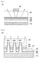
- Figs. 1 and 2 are cross sectional views showing the schematic configurations of prior vertical type light emitting devices.
- a prior light emitting device 100 includes a substrate 110, a p-type conductive layer 120, a p-type semiconductor layer 130, an active layer 140, an n-type semiconductor layer 150 and an n-type electrode pad 160.
- the light emitting device 100 shown in Fig. 1 light which is generated from the active layer 140 and is outward emitted is partially blocked by the uppermost n-type electrode pad 160. Therefore, the light emitting device 100 has low light emission efficiency.
- a prior light emitting device 200 includes a substrate 210, an n-type conductive layer 220, an insulation layer 230, a p-type conductive layer 240, a p-type semiconductor layer 250, an active layer 260, an n-type semiconductor layer 270 and an n-type electrode pad 241.
- the n-type conductive layer 220 includes conductive vias 220a, 220b and 220c penetrating the p-type conductive layer 240, the p-type semiconductor layer 250 and the active layer 260 and contacting with the n-type semiconductor layer 270.
- the upper portion of the light emitting device 200 shown in Fig. 2 is not blocked by an electrode, so that the light emitting device 200 has light-extraction efficiency higher than that of a prior light emitting device.
- the insulation layer 230 is formed in the areas of the conductive vias 220a, 220b and 220c, which project into the n-type semiconductor layer 270. This causes a contact area between the n-type conductive layer 220 and the n-type semiconductor layer 270 to be decreased.
- the sloping surfaces of the conductive vias 220a, 220b and 220c increase with the increases of the depths of the conductive vias 220a, 220b and 220c, so that a contact area between the n-type semiconductor layer 270 and the conductive vias 220a, 220b and 220c is reduced. For this reason, the prior light emitting device having a via electrode shape has limited light-extraction efficiency.
- the light emitting device includes: a conductive support member; a first conductive layer disposed on the conductive support member; a second conductive layer disposed on the first conductive layer; a light emitting structure including a first semiconductor layer placed over the second conductive layer, a second semiconductor layer placed between the first semiconductor layer and the second conductive layer and an active layer placed between the first semiconductor layer and the second semiconductor layer; and an insulation layer placed between the first conductive layer and the second conductive layer.
- the first conductive layer may include at least one via which penetrates the second conductive layer, the second semiconductor layer and the active layer and is disposed within the first semiconductor layer.
- the insulation layer may be disposed to extend along the side of the via.
- the first semiconductor layer may include an ohmic contact layer formed on or above the conductive via.
- the ohmic contact layer may be an Al doped layer.
- the ohmic contact layer may be an AlGaN layer.
- a thickness or a size of each layer may be magnified, omitted or schematically shown for the purpose of convenience and clearness of description.
- the size of each component may not necessarily mean its actual size.
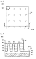
- Fig. 3a is a view showing a top surface of a light emitting device 300 according to a first embodiment of the present invention.
- Figs. 3b and 3c are cross sectional views schematically showing configurations of light emitting devices 300a and 300b according to a first embodiment of the present invention.
- Figs. 3b and 3c are cross sectional views of the light emitting devices 300a and 300b taken along line A-A' of Fig. 3a .
- the light emitting devices 300a and 300b include a conductive support member 310, a first conductive layer 320, a second conductive layer 330, a light emitting structure including a first semiconductor layer 340 placed over the second conductive layer 330, a second semiconductor layer 350 placed between the first semiconductor layer 340 and the second conductive layer 330 and an active layer 360 placed between the first semiconductor layer 340 and the second semiconductor layer 350, an electrode pad 331a, A1 doping layers 341a and 341b, an insulation layer 370 and a passivation layer 380.
- the first conductive layer 320 is an n-type conductive layer
- the second conductive layer 330 is a p-type conductive layer
- the electrode pad 331a is a p-type electrode pad
- the first semiconductor layer 340 is an n-type semiconductor layer
- the second semiconductor layer 350 is a p-type semiconductor layer.
- the conductive support member 310 may be formed including at least one of Au, Ni, A1, Cu, W, Si, Se and GaAs.
- the conductive support member 310 may be made of a metal alloy of Si and Al.
- the n-type conductive layer 320 may include a conductive layer formed on the conductive support member 310, and a plurality of conductive vias 320a connected with each other by the conductive layer.
- the n-type conductive layer 320 may be formed including at least one of Ag, Al, Au, Pt, Ti, Cr and W.
- the conductive via 320a may be formed to penetrate the n-type conductive layer 320, the p-type conductive layer 330, the p-type semiconductor layer 350 and the active layer 360, and to project into a certain area of the n-type semiconductor layer 340.
- the insulation layer 370 may be formed such that the n-type conductive layer 320 is electrically insulated from the layers except for the conductive support member 310 and the n-type semiconductor layer 340. More specifically, the insulation layer 370 is formed between the n-type conductive layer 320 and the p-type conductive layer 330 and formed on the side walls of the plurality of conductive vias 320a, so that the n-type conductive layer 320 can be electrically insulated from the p-type conductive layer 330, the p-type semiconductor layer 350 and the active layer 360.
- the insulation layer 370 may be formed including at least one of silicon oxide (SiO 2 ), silicon nitride (SiO x Ny, Si x N y ), Al 2 O 3 and fluoride based compound.
- the p-type conductive layer 330 may be formed on the insulation layer 370.
- the p-type conductive layer 330 does not exist in the areas which the conductive via 320a penetrates.
- the p-type conductive layer 330 may include at least one of indium tin oxide (ITO), indium zinc oxide (IZO), indium zinc tin oxide (IZTO), indium aluminum zinc oxide (IAZO), indium gallium zinc oxide (IGZO), indium gallium tin oxide (IGTO), aluminum zinc oxide (AZO), antimony tin oxide (ATO), gallium zinc oxide (GZO), IrOx, RuOx, RuOx/ITO, Ni/IrOx/Au, and Ni/IrOx/Au/ITO, Pt, Ni, Au, Rh, Pd, Ag, Al, Ir. This intends to minimize the contact resistance of the p-type semiconductor layer 350 because the p-type conductive layer 330 electrically contacts with the p-type semiconductor layer 350. This also intends to improve light emission efficiency by reflecting outward light generated from the active layer 360.
- the p-type conductive layer 330 may include at least one exposed area 331 of the interface on which the p-type conductive layer 330 contacts with the p-type semiconductor layer 350.
- the p-type electrode pad 331a may be formed in order to connect an external power supply to the p-type conductive layer 330.
- the p-type semiconductor layer 350, the active layer 360 and the n-type semiconductor layer 340 are not formed.
- the p-type electrode pad 331a may be formed in the corners of the light emitting devices 300a and 300b. This intends to maximize the light emitting areas of the light emitting devices 300a and 300b.
- the p-type semiconductor layer 350 may be formed on the p-type conductive layer 330.
- the active layer 360 may be formed on the p-type semiconductor layer 350.
- the n-type semiconductor layer 340 may be formed on the active layer 360.
- the p-type semiconductor layer 350 and the active layer 360 do not exist in the areas which the conductive via 320a penetrates.
- the n-type semiconductor layer 340 may be formed of a semiconductor material having an empirical formula of InxAlyGa( 1-xy )N (0 ⁇ x ⁇ 1, 0 ⁇ y ⁇ 1, 0 ⁇ x+y ⁇ 1), for example, InAlGaN, GaN, AlGaN, InGaN, AlInN, A1N and InN and the like.
- An n-type dopant such as Si, Ge and Sn and the like may be doped in the n-type semiconductor layer 340.
- the n-type semiconductor layer 340 may include the A1 doping layers 341a and 341b formed on the conductive via 320a.
- the A1 doping layer 341a is formed by doping an n-GaN semiconductor layer 340 with Al.
- the amount of carrier (hole concentration) of the n-type semiconductor layer 340 is 1x 1017cm -3 , this affects carrier concentration increase due to the Al doping and does not affect band gap.
- the Al doping layer 341a may be designated as an ohmic contact layer.
- the Al doping layer 341a may be, as shown in Fig. 3b , formed on the top surface of the conductive via 320a. Otherwise, the Al doping layer 341b may be, as shown in Fig. 3c , formed above the conductive via 320a within the n-type semiconductor layer 340.
- the width of a potential barrier formed on a contact surface between metal constituting the conductive via 320a and semiconductor constituting the n-type semiconductor layer 340 is reduced by using a method of increasing doping concentration.
- contact resistance is decreased due to electron tunneling and ohmic contact can be improved.
- the A1 doping layers 341a and 341b concentrate carriers on the top surface of the conductive via 320a, so that the electron tunneling occurs more easily and the ohmic characteristics can be enhanced.
- the Al doping layer may be formed by doping a specific area of a GaN layer with A1 material.
- An AlGaN layer to be described later in another embodiment may be formed by mixing Al and GaN in a certain ratio.
- the top surface of the conductive via 320a may come in direct contact with the n-type semiconductor layer 340. Accordingly, the conductive support member 310 may be electrically connected with the n-type semiconductor layer 340 through the conductive via 320a. In this case, since the n-type conductive layer 320 is electrically connected with the conductive support member 310 and the n-type semiconductor layer 340, it is recommended that the n-type conductive layer 320 be formed of a material having minimal contact resistance with the conductive support member 310 and the n-type semiconductor layer 340.
- the p-type semiconductor layer 350 may be formed of a semiconductor material having an empirical formula of InxAlyGa (1-x-y) N (0 ⁇ x ⁇ 1, 0 ⁇ y ⁇ 1, 0 ⁇ x+y ⁇ 1), for example, InAlGaN, GaN, AlGaN, InGaN, AlInN, A1N and InN and the like.
- a p-type dopant such as Mg and Zn and the like may be doped in the p-type semiconductor layer 350.
- the active layer 360 may be formed of a semiconductor material having an empirical formula ofIn x AlyGa( 1-x-y )N (0 ⁇ x ⁇ 1, 0 ⁇ y ⁇ 1, 0 ⁇ x+y ⁇ 1).
- the active layer 360 may be formed by stacking a plurality of well layers and a plurality of barrier layers, for example, at a cycle of InGaN well layer/GaN barrier layer.
- the active layer 360 may be formed of another material in accordance with the materials constituting the n-type semiconductor layer 340 and the p-type semiconductor layer 350.
- the active layer 360 includes a layer which converts energy by the recombination of electrons and holes into light and emits the light.
- the active layer 360 includes the well layers and the barrier layers, it is recommended that the active layer 360 should be formed such that an energy band gap of the well layer is smaller than that of the barrier layer.
- the active layer 360 exposed outward may function as a current leakage path during the working of the light emitting devices 300a and 300b.
- a problem is prevented by forming the passivation layer 380 on the side wall of the light emitting structure.
- the passivation layer 380 protects the light emitting structure, especially the active layer 360 from the outside and restrains a leakage current from flowing.
- the passivation layer 380 may be formed including at least any one of silicon oxide (SiO 2 ) silicon nitride (SiO x N y , Si x N y ), metal oxide (Al 2 O 3 ) and fluoride based compound.
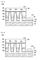
- Figs. 4a and 4b are cross sectional views schematically showing configurations of light emitting devices 400a and 400b according to a second embodiment of the present invention.
- the light emitting devices 400a and 400b include a conductive support member 410, a first conductive layer 420, a second conductive layer 430, a light emitting structure including a first semiconductor layer 440 placed over the second conductive layer 430, a second semiconductor layer 450 placed between the first semiconductor layer 440 and the second conductive layer 430 and an active layer 460 placed between the first semiconductor layer 440 and the second semiconductor layer 450, an electrode pad 431a, AlGaN layers 441a and 441b, an insulation layer 470 and a passivation layer 480.
- the first conductive layer 420 is an n-type conductive layer
- the second conductive layer 430 is a p-type conductive layer
- the electrode pad 431a is a p-type electrode pad
- the first semiconductor layer 440 is an n-type semiconductor layer
- the second semiconductor layer 450 is a p-type semiconductor layer.
- the conductive support member 410 may be formed including at least one of Au, Ni, Al, Cu, W, Si, Se and GaAs.
- the conductive support member 310 may be made of a metal alloy of Si and Al.
- the n-type conductive layer 420 may include a conductive layer formed on the conductive support member 410, and a plurality of conductive vias 420a connected with each other by the conductive layer.
- the n-type conductive layer 420 may be formed including at least one of Ag, Al, Au, Pt, Ti, Cr and W.
- the conductive via 420a may be formed to penetrate the n-type conductive layer 420, the p-type conductive layer 430, the p-type semiconductor layer 450 and the active layer 460, and to project into a certain area of the n-type semiconductor layer 440.
- the insulation layer 470 may be formed such that the n-type conductive layer 420 is electrically insulated from the layers except for the conductive support member 410 and the n-type semiconductor layer 440. More specifically, the insulation layer 470 is formed between the n-type conductive layer 420 and the p-type conductive layer 430 and formed on the side walls of the plurality of conductive vias 420a, so that the n-type conductive layer 420 can be electrically insulated from the p-type conductive layer 430, the p-type semiconductor layer 450 and the active layer 460.
- the insulation layer 470 may be formed including at least one of silicon oxide (SiO 2 ) silicon nitride (SiO x N y , Si x N y ), Al 2 O 3 and fluoride based compound.
- the p-type conductive layer 430 may be formed on the insulation layer 470.
- the p-type conductive layer 430 does not exist in the areas which the conductive via 420a penetrates.
- the p-type conductive layer 430 may include at least one of indium tin oxide (ITO), indium zinc oxide (IZO), indium zinc tin oxide (IZTO), indium aluminum zinc oxide (IAZO), indium gallium zinc oxide (IGZO), indium gallium tin oxide (IGTO), aluminum zinc oxide (AZO), antimony tin oxide (ATO), gallium zinc oxide (GZO), IrOx, RuOx, RuOx/ITO, Ni/IrOx/Au, and Ni/IrOx/Au/ITO, Pt, Ni, Au, Rh, Pd, Ag, Al, Ir.
- ITO indium tin oxide
- IZO indium zinc oxide
- IZTO indium aluminum zinc oxide
- IGZO indium gallium zinc oxide
- IGTO indium gallium tin oxide
- ATO antimony tin oxide
- GZO gallium zinc oxide
- the p-type conductive layer 430 may include at least one exposed area 431 of the interface on which the p-type conductive layer 430 contacts with the p-type semiconductor layer 450.
- the p-type electrode pad 431a may be formed in order to connect an external power supply to the p-type conductive layer 430.
- the p-type semiconductor layer 450, the active layer 460 and the n-type semiconductor layer 440 are not formed.
- the p-type electrode pad 431a may be formed in the corners of the light emitting devices 400a and 400b. This intends to maximize the light emitting areas of the light emitting devices 400a and 400b.
- the p-type semiconductor layer 450 may be formed on the p-type conductive layer 430.
- the active layer 460 may be formed on the p-type semiconductor layer 450.
- the n-type semiconductor layer 440 may be formed on the active layer 460.
- the p-type semiconductor layer 450 and the active layer 460 do not exist in the areas which the conductive via 420a penetrates.
- the n-type semiconductor layer 440 may be formed of a semiconductor material having an empirical formula of InxAlyGa( 1-x-y )N (0 ⁇ x ⁇ 1, 0 ⁇ y ⁇ 1, 0 ⁇ x+y ⁇ 1), for example, InAlGaN, GaN, AlGaN, InGaN, AlInN, A1N and InN and the like.
- An n-type dopant such as Si, Ge and Sn and the like may be doped in the n-type semiconductor layer 340.
- the n-type semiconductor layer 440 may include the AlGaN layers 441a and 441b formed on the conductive via 420a.
- the AlGaN layer 441a may be, as shown in Fig. 4a , formed on the top surface of the conductive via 420a.
- the AlGaN layer 441b may be, as shown in Fig. 4b , formed above the conductive via 420a within the n-type semiconductor layer 440.
- the AlGaN layers 441a and 441b may be formed by growing a cap layer on an n-GaN semiconductor layer 440.
- the AlGaN layers 441a and 441b have an empirical formula of Al x Ga (1-x) N (0 ⁇ x ⁇ 1), influences a mole fraction of group III element in accordance with the amount of Al, and gives variety to band gap depending on the influence.
- the AlGaN layer 441a may be designated as an ohmic contact layer.
- the AlGaN layers 441a and 441b as a material which belongs to the same group as that of the n-GaN semiconductor layer 440 and has a band gap different from that of the n-GaN semiconductor layer 440, reduce a depletion region between the conductive via 420a and the n-GaN semiconductor layer 440 or lower a surface Schottky barrier between the conductive via 420a and the n-GaN semiconductor layer 440 by causing spontaneous polarization and piezoelectric polarization. As a result, ohmic characteristic can be improved.
- the AlGaN layer 441a is formed as shown in Fig. 4b , the top surface of the conductive via 420a may come in direct contact with the n-type semiconductor layer 440. Accordingly, the conductive support member 410 may be electrically connected with the n-type semiconductor layer 440 through the conductive via 420a. In this case, since the n-type conductive layer 420 is electrically connected with the conductive support member 410 and the n-type semiconductor layer 440, it is recommended that the n-type conductive layer 420 be formed of a material having minimal contact resistance with the conductive support member 410 and the n-type semiconductor layer 440.
- the p-type semiconductor layer 450 may be formed of a semiconductor material having an empirical formula of InxAlyGa( 1-x-y) N (0 ⁇ x ⁇ 1, 0 ⁇ y ⁇ 1, 0 ⁇ x+y ⁇ 1), for example, InAlGaN, GaN, AlGaN, InGaN, AlInN, AlN and InN and the like.
- a p-type dopant such as Mg and Zn and the like may be doped in the p-type semiconductor layer 450.
- the active layer 460 may be formed of a semiconductor material having an empirical formula ofIn x A1yGa (1-x-y) N (0 ⁇ x ⁇ 1, 0 ⁇ y ⁇ 1, 0 ⁇ x+y ⁇ 1).
- the active layer 460 may be formed by stacking a plurality of well layers and a plurality of barrier layers, for example, at a cycle of InGaN well layer/GaN barrier layer.
- the active layer 460 may be formed of another material in accordance with the materials constituting the n-type semiconductor layer 340 and the p-type semiconductor layer 450. In other words, the active layer 460 converts energy by the recombination of electrons and holes into light and emits. Therefore, it is recommended that the active layer 460 be formed of a material having an energy band gap smaller than those of the n-type semiconductor layer 440 and the p-type semiconductor layer 450.
- the active layer 460 exposed outward may function as a current leakage path during the working of the light emitting devices 400a and 400b.
- a problem is prevented by forming the passivation layer 480 on the side wall of the light emitting structure.
- the passivation layer 480 protects the light emitting structure, especially the active layer 460 from the outside and restrains a leakage current from flowing.
- the passivation layer 480 may be formed including at least any one of silicon oxide (SiO 2 ) silicon nitride (SiO x N y , Si x N y ), metal oxide (Al 2 O 3 ) and fluoride based compound.
- Fig. 5 is a cross sectional view showing schematically a light emitting device package 1000.
- the light emitting device package 1000 includes a package body 1100, a first electrode layer 1110, a second electrode 1120, a light emitting device 1200 and a filler 1300.
- the package body 1100 may be formed including a silicon material, a synthetic resin material or a metallic material. Inclined surfaces are formed around the light emitting device 1200, thereby improving the light-extraction efficiency.
- the first electrode layer 1110 and the second electrode 1120 are disposed in the package body 1100.
- the first electrode layer 1110 and the second electrode 1120 are electrically isolated from each other and supply electric power to the light emitting device 1200.
- the first electrode layer 1110 and the second electrode 1120 are able to increase luminous efficiency by reflecting light generated from the light emitting device 1200.
- the first electrode layer 1110 and the second electrode 1120 can also exhaust heat generated from the light emitting device 1200.
- the light emitting device 1200 is electrically connected to the first electrode layer 1110 and the second electrode 1120.
- the light emitting device 1200 may be disposed on the package body 1100 or may be disposed on either the first electrode layer 1110 or the second electrode 1120.
- the light emitting device 1200 may be also electrically connected to the first electrode layer 1110 and the second electrode 1120 by any one of a wire bonding manner, a flip-chip manner or a die-bonding process.
- the filler 1300 may be formed to surround and protect the light emitting device 1200.
- the filler 1300 includes a fluorescent material, so that the wavelength of light emitted from the light emitting device 1200 may be changed.
- the light emitting device package 1000 is equipped with at least one or a plurality of the light emitting devices disclosed in the embodiments. There is no limited to the number of the light emitting devices.
- a plurality of the light emitting device packages 1000 according to the embodiment may be arrayed on a substrate.
- An optical member such as a light guide plate, a prism sheet and a diffusion sheet and the like may be disposed on the optical path of the light emitting device package 1000.
- Such a light emitting device package 1000, the substrate and the optical member are able to function as a light unit.
- Another embodiment can be implemented by a display device, a pointing device and a lighting device and the like, all of which include the semiconductor light emitting device or the light emitting device package which has been described in the aforementioned embodiments.
- the lighting device may include a lamp and a street lamp.
- Fig. 6 is a perspective view showing a lighting device 1500 including the light emitting device package shown in Fig. 4 .
- the lighting device 1500 may include a case 1510, a light emitting module 1530 disposed on the case 1510, a cover 1550 connected to the case 1510, and a connection terminal 1570 connected to the case 1510 and supplied with an electric power from an external power supply.
- the case 1510 may be formed of a material having an excellent heat radiating characteristic, for example, a metal material or a resin material.
- the light emitting module 1530 may include a board 1531 and at least one light emitting device package 1533 which is based on the embodiment and is mounted on the board 1531.
- the plurality of the light emitting device packages 1533 may be radially arranged apart from each other at a predetermined interval on the board 1531.
- the board 1531 may be an insulating substrate on which a circuit pattern has been printed, and may include, for example, a printed circuit board (PCB), a metal core PCB, a flexible PCB, a ceramic PCB, an FR-4 substrate, etc.
- PCB printed circuit board
- metal core PCB metal core PCB
- flexible PCB flexible PCB
- ceramic PCB ceramic PCB
- FR-4 substrate etc.
- the board 1531 may be formed of a material capable of efficiently reflecting light.
- the surface of the board 1531 may have a color capable of efficiently reflecting light, such as white or silver.
- the at least one light emitting device package 1533 may be disposed on the board 1531.
- Each of the light emitting device packages 1533 may include at least one light emitting diode (LED) chip.
- the LED chip may include both a LED emitting red, green, blue or white light and a UV LED emitting ultraviolet (UV).
- the light emitting module 1530 may have various combinations of the light emitting device packages so as to obtain desired color and luminance.
- the light emitting module 1530 may have a combination of a white LED, a red LED and a green LED in order to obtain a high color rendering index (CRI).
- CRI color rendering index
- connection terminal 1570 may be electrically connected to the light emitting module 1530 in order to supply power.
- the connection terminal 1570 may be screwed and connected to an external power in the form of a socket.
- the connection terminal 1570 may be made in the form of a pin and inserted into the external power, or may be connected to the external power through a power line.
- any reference in this specification to "one embodiment,” “an embodiment,” “example embodiment,” etc. means that a particular feature, structure, or characteristic described in connection with the embodiment is included in at least one embodiment of the invention.
- the appearances of such phrases in various places in the specification are not necessarily all referring to the same embodiment.
Landscapes
- Led Devices (AREA)
- Electroluminescent Light Sources (AREA)
Abstract
Description
- The present application claims priority under 35 U.S.C. § 119(e) of Korean Patent Application No.
10-2010-0097280 filed on October 6, 2010 - The present invention relates to a light emitting device and a lighting system.
- A light emitting diode (LED) is a semiconductor element for converting electric energy into light. As compared with existing light sources such as a fluorescent lamp and an incandescent electric lamp and so on, the LED has advantages of low power consumption, a semi-permanent span of life, a rapid response speed, safety and an environment-friendliness. For this reason, many researches are devoted to substitution of the existing light sources with the LED. The LED is now increasingly used as a light source for lighting devices, for example, various lamps used interiorly and exteriorly, a liquid crystal display device, an electric sign and a street lamp and the like.
-
Figs. 1 and 2 are cross sectional views showing the schematic configurations of prior vertical type light emitting devices. - First, referring to
Fig. 1 , a priorlight emitting device 100 includes asubstrate 110, a p-typeconductive layer 120, a p-type semiconductor layer 130, anactive layer 140, an n-type semiconductor layer 150 and an n-type electrode pad 160. - Regarding the
light emitting device 100 shown inFig. 1 , light which is generated from theactive layer 140 and is outward emitted is partially blocked by the uppermost n-type electrode pad 160. Therefore, thelight emitting device 100 has low light emission efficiency. - Next, referring to
Fig. 2 , a priorlight emitting device 200 includes asubstrate 210, an n-typeconductive layer 220, aninsulation layer 230, a p-typeconductive layer 240, a p-type semiconductor layer 250, anactive layer 260, an n-type semiconductor layer 270 and an n-type electrode pad 241. The n-typeconductive layer 220 includesconductive vias conductive layer 240, the p-type semiconductor layer 250 and theactive layer 260 and contacting with the n-type semiconductor layer 270. - Unlike the
light emitting device 100 shown inFig. 1 , the upper portion of thelight emitting device 200 shown inFig. 2 is not blocked by an electrode, so that thelight emitting device 200 has light-extraction efficiency higher than that of a prior light emitting device. - However, the
insulation layer 230 is formed in the areas of theconductive vias type semiconductor layer 270. This causes a contact area between the n-typeconductive layer 220 and the n-type semiconductor layer 270 to be decreased. The sloping surfaces of theconductive vias conductive vias type semiconductor layer 270 and theconductive vias - One embodiment is a light emitting device. The light emitting device includes: a conductive support member; a first conductive layer disposed on the conductive support member; a second conductive layer disposed on the first conductive layer; a light emitting structure including a first semiconductor layer placed over the second conductive layer, a second semiconductor layer placed between the first semiconductor layer and the second conductive layer and an active layer placed between the first semiconductor layer and the second semiconductor layer; and an insulation layer placed between the first conductive layer and the second conductive layer. The first conductive layer may include at least one via which penetrates the second conductive layer, the second semiconductor layer and the active layer and is disposed within the first semiconductor layer. The insulation layer may be disposed to extend along the side of the via. The first semiconductor layer may include an ohmic contact layer formed on or above the conductive via.
- According to the embodiment, the ohmic contact layer may be an Al doped layer.
- The ohmic contact layer may be an AlGaN layer.
- Arrangements and embodiments may be described in detail with reference to the following drawings in which like reference numerals refer to like elements and wherein:
-
Figs. 1 and 2 are cross sectional views showing the schematic configurations of prior vertical light emitting devices. -
Fig. 3a is a view showing a top surface of a light emitting device according to a first embodiment of the present invention. -
Figs. 3b and3c are cross sectional views schematically showing a configuration of the light emitting device according to a first embodiment of the present invention. -
Figs. 4a and4b are cross sectional views schematically showing a configuration of a light emitting device according to a second embodiment of the present invention. -
Fig. 5 is a view schematically showing a light emitting device package. -
Fig. 6 is a view schematically showing a lighting device. - A thickness or a size of each layer may be magnified, omitted or schematically shown for the purpose of convenience and clearness of description. The size of each component may not necessarily mean its actual size.
- It should be understood that when an element is referred to as being 'on' or "under" another element, it may be directly on/under the element, and/or one or more intervening elements may also be present. When an element is referred to as being 'on' or 'under', 'under the element' as well as 'on the element' may be included based on the element.
- An embodiment may be described in detail with reference to the accompanying drawings.
-
Fig. 3a is a view showing a top surface of alight emitting device 300 according to a first embodiment of the present invention. -
Figs. 3b and3c are cross sectional views schematically showing configurations oflight emitting devices Figs. 3b and3c are cross sectional views of thelight emitting devices Fig. 3a . - First, referring to
Figs .3b and3c , thelight emitting devices conductive support member 310, a firstconductive layer 320, a secondconductive layer 330, a light emitting structure including afirst semiconductor layer 340 placed over the secondconductive layer 330, asecond semiconductor layer 350 placed between thefirst semiconductor layer 340 and the secondconductive layer 330 and anactive layer 360 placed between thefirst semiconductor layer 340 and thesecond semiconductor layer 350, anelectrode pad 331a, A1doping layers insulation layer 370 and apassivation layer 380. - Hereafter, for convenience of description, it is assumed that the first
conductive layer 320 is an n-type conductive layer, the secondconductive layer 330 is a p-type conductive layer, theelectrode pad 331a is a p-type electrode pad, thefirst semiconductor layer 340 is an n-type semiconductor layer, and thesecond semiconductor layer 350 is a p-type semiconductor layer. - The
conductive support member 310 may be formed including at least one of Au, Ni, A1, Cu, W, Si, Se and GaAs. For example, theconductive support member 310 may be made of a metal alloy of Si and Al. - The n-type
conductive layer 320 may include a conductive layer formed on theconductive support member 310, and a plurality ofconductive vias 320a connected with each other by the conductive layer. The n-typeconductive layer 320 may be formed including at least one of Ag, Al, Au, Pt, Ti, Cr and W. - As shown in
Figs. 3b and3c , the conductive via 320a may be formed to penetrate the n-typeconductive layer 320, the p-typeconductive layer 330, the p-type semiconductor layer 350 and theactive layer 360, and to project into a certain area of the n-type semiconductor layer 340. - The
insulation layer 370 may be formed such that the n-typeconductive layer 320 is electrically insulated from the layers except for theconductive support member 310 and the n-type semiconductor layer 340. More specifically, theinsulation layer 370 is formed between the n-typeconductive layer 320 and the p-typeconductive layer 330 and formed on the side walls of the plurality ofconductive vias 320a, so that the n-typeconductive layer 320 can be electrically insulated from the p-typeconductive layer 330, the p-type semiconductor layer 350 and theactive layer 360. Theinsulation layer 370 may be formed including at least one of silicon oxide (SiO2), silicon nitride (SiOxNy, SixNy), Al2O3 and fluoride based compound. - The p-type
conductive layer 330 may be formed on theinsulation layer 370. The p-typeconductive layer 330 does not exist in the areas which the conductive via 320a penetrates. - The p-type
conductive layer 330 may include at least one of indium tin oxide (ITO), indium zinc oxide (IZO), indium zinc tin oxide (IZTO), indium aluminum zinc oxide (IAZO), indium gallium zinc oxide (IGZO), indium gallium tin oxide (IGTO), aluminum zinc oxide (AZO), antimony tin oxide (ATO), gallium zinc oxide (GZO), IrOx, RuOx, RuOx/ITO, Ni/IrOx/Au, and Ni/IrOx/Au/ITO, Pt, Ni, Au, Rh, Pd, Ag, Al, Ir. This intends to minimize the contact resistance of the p-type semiconductor layer 350 because the p-typeconductive layer 330 electrically contacts with the p-type semiconductor layer 350. This also intends to improve light emission efficiency by reflecting outward light generated from theactive layer 360. - The p-type
conductive layer 330 may include at least one exposedarea 331 of the interface on which the p-typeconductive layer 330 contacts with the p-type semiconductor layer 350. On the exposed area, the p-type electrode pad 331a may be formed in order to connect an external power supply to the p-typeconductive layer 330. On the exposedarea 331, the p-type semiconductor layer 350, theactive layer 360 and the n-type semiconductor layer 340 are not formed. The p-type electrode pad 331a may be formed in the corners of thelight emitting devices light emitting devices - The p-
type semiconductor layer 350 may be formed on the p-typeconductive layer 330. Theactive layer 360 may be formed on the p-type semiconductor layer 350. The n-type semiconductor layer 340 may be formed on theactive layer 360. The p-type semiconductor layer 350 and theactive layer 360 do not exist in the areas which the conductive via 320a penetrates. - The n-
type semiconductor layer 340 may be formed of a semiconductor material having an empirical formula of InxAlyGa(1-xy)N (0≤x≤1, 0 ≤y≤1, 0≤x+y≤1), for example, InAlGaN, GaN, AlGaN, InGaN, AlInN, A1N and InN and the like. An n-type dopant such as Si, Ge and Sn and the like may be doped in the n-type semiconductor layer 340. - The n-
type semiconductor layer 340 may include theA1 doping layers A1 doping layer 341a is formed by doping an n-GaN semiconductor layer 340 with Al. When the amount of carrier (hole concentration) of the n-type semiconductor layer 340 is 1x 1017cm-3, this affects carrier concentration increase due to the Al doping and does not affect band gap. TheAl doping layer 341a may be designated as an ohmic contact layer. - The
Al doping layer 341a may be, as shown inFig. 3b , formed on the top surface of the conductive via 320a. Otherwise, theAl doping layer 341b may be, as shown inFig. 3c , formed above the conductive via 320a within the n-type semiconductor layer 340. - In order to improve ohmic characteristics of the top surface of the conductive via 320a, there is a method of reducing the width of a potential barrier formed on a contact surface between metal constituting the conductive via 320a and semiconductor constituting the n-
type semiconductor layer 340. When the width of the potential barrier is reduced by using a method of increasing doping concentration, contact resistance is decreased due to electron tunneling and ohmic contact can be improved. As a result, theA1 doping layers - In the embodiment, the Al doping layer may be formed by doping a specific area of a GaN layer with A1 material. An AlGaN layer to be described later in another embodiment may be formed by mixing Al and GaN in a certain ratio.
- Meanwhile, the
A1 doping layer 341b is formed as shown inFig. 3b , the top surface of the conductive via 320a may come in direct contact with the n-type semiconductor layer 340. Accordingly, theconductive support member 310 may be electrically connected with the n-type semiconductor layer 340 through the conductive via 320a. In this case, since the n-typeconductive layer 320 is electrically connected with theconductive support member 310 and the n-type semiconductor layer 340, it is recommended that the n-typeconductive layer 320 be formed of a material having minimal contact resistance with theconductive support member 310 and the n-type semiconductor layer 340. - The p-
type semiconductor layer 350 may be formed of a semiconductor material having an empirical formula of InxAlyGa(1-x-y)N (0≤x≤1, 0 ≤y≤1, 0≤x+y≤1), for example, InAlGaN, GaN, AlGaN, InGaN, AlInN, A1N and InN and the like. A p-type dopant such as Mg and Zn and the like may be doped in the p-type semiconductor layer 350. - The
active layer 360 may be formed of a semiconductor material having an empirical formula ofInxAlyGa(1-x-y)N (0≤x≤1, 0≤y≤1, 0≤x+y≤1). When theactive layer 360 is formed in a multiple quantum well (MQW) structure, theactive layer 360 may be formed by stacking a plurality of well layers and a plurality of barrier layers, for example, at a cycle of InGaN well layer/GaN barrier layer. - The
active layer 360 may be formed of another material in accordance with the materials constituting the n-type semiconductor layer 340 and the p-type semiconductor layer 350. In other words, theactive layer 360 includes a layer which converts energy by the recombination of electrons and holes into light and emits the light. When theactive layer 360 includes the well layers and the barrier layers, it is recommended that theactive layer 360 should be formed such that an energy band gap of the well layer is smaller than that of the barrier layer. - Meanwhile, the
active layer 360 exposed outward may function as a current leakage path during the working of thelight emitting devices passivation layer 380 on the side wall of the light emitting structure. Thepassivation layer 380 protects the light emitting structure, especially theactive layer 360 from the outside and restrains a leakage current from flowing. Thepassivation layer 380 may be formed including at least any one of silicon oxide (SiO2) silicon nitride (SiOxNy, SixNy), metal oxide (Al2O3) and fluoride based compound. -
Figs. 4a and4b are cross sectional views schematically showing configurations of light emittingdevices 400a and 400b according to a second embodiment of the present invention. - First, referring to
Figs. 4a and4b , thelight emitting devices 400a and 400b according to the second embodiment of the present invention include aconductive support member 410, a firstconductive layer 420, a secondconductive layer 430, a light emitting structure including afirst semiconductor layer 440 placed over the secondconductive layer 430, asecond semiconductor layer 450 placed between thefirst semiconductor layer 440 and the secondconductive layer 430 and anactive layer 460 placed between thefirst semiconductor layer 440 and thesecond semiconductor layer 450, anelectrode pad 431a,AlGaN layers insulation layer 470 and apassivation layer 480. - Hereafter, for convenience of description, it is assumed that the first
conductive layer 420 is an n-type conductive layer, the secondconductive layer 430 is a p-type conductive layer, theelectrode pad 431a is a p-type electrode pad, thefirst semiconductor layer 440 is an n-type semiconductor layer, and thesecond semiconductor layer 450 is a p-type semiconductor layer. - The
conductive support member 410 may be formed including at least one of Au, Ni, Al, Cu, W, Si, Se and GaAs. For example, theconductive support member 310 may be made of a metal alloy of Si and Al. - The n-type
conductive layer 420 may include a conductive layer formed on theconductive support member 410, and a plurality ofconductive vias 420a connected with each other by the conductive layer. The n-typeconductive layer 420 may be formed including at least one of Ag, Al, Au, Pt, Ti, Cr and W. - As shown in
Figs. 4a and4b , the conductive via 420a may be formed to penetrate the n-typeconductive layer 420, the p-typeconductive layer 430, the p-type semiconductor layer 450 and theactive layer 460, and to project into a certain area of the n-type semiconductor layer 440. - The
insulation layer 470 may be formed such that the n-typeconductive layer 420 is electrically insulated from the layers except for theconductive support member 410 and the n-type semiconductor layer 440. More specifically, theinsulation layer 470 is formed between the n-typeconductive layer 420 and the p-typeconductive layer 430 and formed on the side walls of the plurality of conductive vias 420a, so that the n-typeconductive layer 420 can be electrically insulated from the p-typeconductive layer 430, the p-type semiconductor layer 450 and theactive layer 460. Theinsulation layer 470 may be formed including at least one of silicon oxide (SiO2) silicon nitride (SiOxNy, SixNy), Al2O3 and fluoride based compound. - The p-type
conductive layer 430 may be formed on theinsulation layer 470. The p-typeconductive layer 430 does not exist in the areas which the conductive via 420a penetrates. - The p-type
conductive layer 430 may include at least one of indium tin oxide (ITO), indium zinc oxide (IZO), indium zinc tin oxide (IZTO), indium aluminum zinc oxide (IAZO), indium gallium zinc oxide (IGZO), indium gallium tin oxide (IGTO), aluminum zinc oxide (AZO), antimony tin oxide (ATO), gallium zinc oxide (GZO), IrOx, RuOx, RuOx/ITO, Ni/IrOx/Au, and Ni/IrOx/Au/ITO, Pt, Ni, Au, Rh, Pd, Ag, Al, Ir. This intends to minimize the contact resistance of the p-type semiconductor layer 450 because the p-typeconductive layer 430 electrically contacts with the p-type semiconductor layer 450. This also intends to improve light emission efficiency by reflecting outward light generated from theactive layer 460. - The p-type
conductive layer 430 may include at least one exposedarea 431 of the interface on which the p-typeconductive layer 430 contacts with the p-type semiconductor layer 450. On the exposed area, the p-type electrode pad 431a may be formed in order to connect an external power supply to the p-typeconductive layer 430. On the exposedarea 431, the p-type semiconductor layer 450, theactive layer 460 and the n-type semiconductor layer 440 are not formed. The p-type electrode pad 431a may be formed in the corners of thelight emitting devices 400a and 400b. This intends to maximize the light emitting areas of thelight emitting devices 400a and 400b. - The p-
type semiconductor layer 450 may be formed on the p-typeconductive layer 430. Theactive layer 460 may be formed on the p-type semiconductor layer 450. The n-type semiconductor layer 440 may be formed on theactive layer 460. The p-type semiconductor layer 450 and theactive layer 460 do not exist in the areas which the conductive via 420a penetrates. - The n-
type semiconductor layer 440 may be formed of a semiconductor material having an empirical formula of InxAlyGa(1-x-y)N (0≤x≤1, 0 ≤y≤1, 0≤x+y≤1), for example, InAlGaN, GaN, AlGaN, InGaN, AlInN, A1N and InN and the like. An n-type dopant such as Si, Ge and Sn and the like may be doped in the n-type semiconductor layer 340. - The n-
type semiconductor layer 440 may include theAlGaN layers AlGaN layer 441a may be, as shown inFig. 4a , formed on the top surface of the conductive via 420a. Otherwise, theAlGaN layer 441b may be, as shown inFig. 4b , formed above the conductive via 420a within the n-type semiconductor layer 440. The AlGaN layers 441a and 441b may be formed by growing a cap layer on an n-GaN semiconductor layer 440. The AlGaN layers 441a and 441b have an empirical formula of AlxGa(1-x)N (0<x≤1), influences a mole fraction of group III element in accordance with the amount of Al, and gives variety to band gap depending on the influence. TheAlGaN layer 441a may be designated as an ohmic contact layer. - The AlGaN layers 441a and 441b as a material, which belongs to the same group as that of the n-
GaN semiconductor layer 440 and has a band gap different from that of the n-GaN semiconductor layer 440, reduce a depletion region between the conductive via 420a and the n-GaN semiconductor layer 440 or lower a surface Schottky barrier between the conductive via 420a and the n-GaN semiconductor layer 440 by causing spontaneous polarization and piezoelectric polarization. As a result, ohmic characteristic can be improved. - Meanwhile, the
AlGaN layer 441a is formed as shown inFig. 4b , the top surface of the conductive via 420a may come in direct contact with the n-type semiconductor layer 440. Accordingly, theconductive support member 410 may be electrically connected with the n-type semiconductor layer 440 through the conductive via 420a. In this case, since the n-typeconductive layer 420 is electrically connected with theconductive support member 410 and the n-type semiconductor layer 440, it is recommended that the n-typeconductive layer 420 be formed of a material having minimal contact resistance with theconductive support member 410 and the n-type semiconductor layer 440. - The p-
type semiconductor layer 450 may be formed of a semiconductor material having an empirical formula of InxAlyGa(1-x-y)N (0≤x≤1, 0 ≤y≤1, 0≤x+y≤1), for example, InAlGaN, GaN, AlGaN, InGaN, AlInN, AlN and InN and the like. A p-type dopant such as Mg and Zn and the like may be doped in the p-type semiconductor layer 450. - The
active layer 460 may be formed of a semiconductor material having an empirical formula ofInxA1yGa(1-x-y)N (0≤x≤1, 0≤y≤1, 0≤x+y≤1). When theactive layer 460 is formed in a multiple quantum well (MQW) structure, theactive layer 460 may be formed by stacking a plurality of well layers and a plurality of barrier layers, for example, at a cycle of InGaN well layer/GaN barrier layer. - The
active layer 460 may be formed of another material in accordance with the materials constituting the n-type semiconductor layer 340 and the p-type semiconductor layer 450. In other words, theactive layer 460 converts energy by the recombination of electrons and holes into light and emits. Therefore, it is recommended that theactive layer 460 be formed of a material having an energy band gap smaller than those of the n-type semiconductor layer 440 and the p-type semiconductor layer 450. - Meanwhile, the
active layer 460 exposed outward may function as a current leakage path during the working of thelight emitting devices 400a and 400b. Here, such a problem is prevented by forming thepassivation layer 480 on the side wall of the light emitting structure. Thepassivation layer 480 protects the light emitting structure, especially theactive layer 460 from the outside and restrains a leakage current from flowing. Thepassivation layer 480 may be formed including at least any one of silicon oxide (SiO2) silicon nitride (SiOxNy, SixNy), metal oxide (Al2O3) and fluoride based compound. - Hereafter, a light emitting device package according to an embodiment will be described with reference to
Fig. 5. Fig. 5 is a cross sectional view showing schematically a light emittingdevice package 1000. - As shown in
Fig. 5 , the light emittingdevice package 1000 according to the embodiment includes apackage body 1100, afirst electrode layer 1110, asecond electrode 1120, alight emitting device 1200 and afiller 1300. - The
package body 1100 may be formed including a silicon material, a synthetic resin material or a metallic material. Inclined surfaces are formed around thelight emitting device 1200, thereby improving the light-extraction efficiency. - The
first electrode layer 1110 and thesecond electrode 1120 are disposed in thepackage body 1100. Thefirst electrode layer 1110 and thesecond electrode 1120 are electrically isolated from each other and supply electric power to thelight emitting device 1200. Thefirst electrode layer 1110 and thesecond electrode 1120 are able to increase luminous efficiency by reflecting light generated from thelight emitting device 1200. Thefirst electrode layer 1110 and thesecond electrode 1120 can also exhaust heat generated from thelight emitting device 1200. - The
light emitting device 1200 is electrically connected to thefirst electrode layer 1110 and thesecond electrode 1120. Thelight emitting device 1200 may be disposed on thepackage body 1100 or may be disposed on either thefirst electrode layer 1110 or thesecond electrode 1120. - The
light emitting device 1200 may be also electrically connected to thefirst electrode layer 1110 and thesecond electrode 1120 by any one of a wire bonding manner, a flip-chip manner or a die-bonding process. - The
filler 1300 may be formed to surround and protect thelight emitting device 1200. Thefiller 1300 includes a fluorescent material, so that the wavelength of light emitted from thelight emitting device 1200 may be changed. - The light emitting
device package 1000 is equipped with at least one or a plurality of the light emitting devices disclosed in the embodiments. There is no limited to the number of the light emitting devices. - A plurality of the light emitting
device packages 1000 according to the embodiment may be arrayed on a substrate. An optical member such as a light guide plate, a prism sheet and a diffusion sheet and the like may be disposed on the optical path of the light emittingdevice package 1000. Such a light emittingdevice package 1000, the substrate and the optical member are able to function as a light unit. - Another embodiment can be implemented by a display device, a pointing device and a lighting device and the like, all of which include the semiconductor light emitting device or the light emitting device package which has been described in the aforementioned embodiments. For example, the lighting device may include a lamp and a street lamp.
-
Fig. 6 is a perspective view showing alighting device 1500 including the light emitting device package shown inFig. 4 . - Referring to
Fig. 6 , thelighting device 1500 may include acase 1510, alight emitting module 1530 disposed on thecase 1510, acover 1550 connected to thecase 1510, and aconnection terminal 1570 connected to thecase 1510 and supplied with an electric power from an external power supply. - The
case 1510 may be formed of a material having an excellent heat radiating characteristic, for example, a metal material or a resin material. - The
light emitting module 1530 may include aboard 1531 and at least one light emittingdevice package 1533 which is based on the embodiment and is mounted on theboard 1531. The plurality of the light emittingdevice packages 1533 may be radially arranged apart from each other at a predetermined interval on theboard 1531. - The
board 1531 may be an insulating substrate on which a circuit pattern has been printed, and may include, for example, a printed circuit board (PCB), a metal core PCB, a flexible PCB, a ceramic PCB, an FR-4 substrate, etc. - Also, the
board 1531 may be formed of a material capable of efficiently reflecting light. The surface of theboard 1531 may have a color capable of efficiently reflecting light, such as white or silver. - The at least one light emitting
device package 1533 may be disposed on theboard 1531. Each of the light emittingdevice packages 1533 may include at least one light emitting diode (LED) chip. The LED chip may include both a LED emitting red, green, blue or white light and a UV LED emitting ultraviolet (UV). - The
light emitting module 1530 may have various combinations of the light emitting device packages so as to obtain desired color and luminance. For example, thelight emitting module 1530 may have a combination of a white LED, a red LED and a green LED in order to obtain a high color rendering index (CRI). - The
connection terminal 1570 may be electrically connected to thelight emitting module 1530 in order to supply power. Theconnection terminal 1570 may be screwed and connected to an external power in the form of a socket. However, there is no limit to the method for connecting theconnection terminal 1570 to an external power. For example, theconnection terminal 1570 may be made in the form of a pin and inserted into the external power, or may be connected to the external power through a power line. - Any reference in this specification to "one embodiment," "an embodiment," "example embodiment," etc., means that a particular feature, structure, or characteristic described in connection with the embodiment is included in at least one embodiment of the invention. The appearances of such phrases in various places in the specification are not necessarily all referring to the same embodiment. Further, when a particular feature, structure, or characteristic is described in connection with any embodiment, it is submitted that it is within the purview of one skilled in the art to affect such feature, structure, or characteristic in connection with other ones of the embodiments.
- Although embodiments have been described with reference to a number of illustrative embodiments thereof, it should be understood that numerous other modifications and embodiments can be devised by those skilled in the art that will fall within the spirit and scope of the principles of this disclosure. More particularly, various variations and modifications are possible in the component parts and/or arrangements of the subject combination arrangement within the scope of the disclosure, the drawings and the appended claims. In addition to variations and modifications in the component parts and/or arrangements, alternative uses will also be apparent to those skilled in the art.
Claims (13)
- A light emitting device comprising:a conductive support member;a first conductive layer disposed on the conductive support member;a second conductive layer disposed on the first conductive layer;a light emitting structure including a first semiconductor layer placed over the second conductive layer, a second semiconductor layer placed between the first semiconductor layer and the second conductive layer and an active layer placed between the first semiconductor layer and the second semiconductor layer; andan insulation layer placed between the first conductive layer and the second conductive layer,
wherein the first conductive layer includes at least one via which penetrates the second conductive layer, the second semiconductor layer and the active layer and is disposed within the first semiconductor layer,
wherein the insulation layer is disposed to extend along the side of the via, and
wherein the first semiconductor layer includes an ohmic contact layer formed on or above the conductive via. - The light emitting device of claim 1, wherein the ohmic contact layer is an Al doped layer.
- The light emitting device of claim 1, wherein the ohmic contact layer is an AlGaN layer.
- The light emitting device of claim 1, further comprising a passivation layer which is formed on a side wall of the light emitting structure.
- The light emitting device of claim 1, wherein the second conductive layer comprises at least one exposed area of surface forming an interface with the second semiconductor layer, and further comprises an electrode pad formed on the exposed area of the second conductive layer.
- The light emitting device of claim 1, wherein the conductive support member comprises at least one of Au, Ni, Al, Cu, W, Si, Se and GaAs.
- The light emitting device of claim 1, wherein the first conductive layer comprises at least one of Ag, Al, Au, Pt, Ti, Cr and W.
- The light emitting device of claim 1, wherein the second conductive layer comprises at least one of Ag, Al, Pt, Ni, Pt, Pd, Au, Ir and a transparent conductive oxide, and wherein the transparent conductive oxide comprises at least one of ITO and GZO.
- The light emitting device of claim 1, wherein the top surface of the via has an area greater than that of the bottom surface of the via.
- The light emitting device of claim 4, wherein the insulation layer and the passivation layer are respectively formed including at least any one of silicon oxide, silicon nitride, metal oxide and fluoride based compound.
- The light emitting device of claim 1, wherein the active layer is formed by stacking a plurality of well layers and a plurality of barrier layers.
- A light emitting device package comprising:a package body;a first electrode layer and a second electrode layer, all of which are disposed on the package body; anda light emitting device electrically connected to the first electrode layer and the second electrode layer,
wherein the light emitting device is dependent on any one claim of claims 1 to 11. - A lighting device comprising:a case;a light emitting module disposed within the case; anda connection terminal disposed within the case and electrically connected to the light emitting module in such a manner as to be supplied with an electric power from an external power supply,
wherein the light emitting module includes an light emitting device package according to claim 12.
Applications Claiming Priority (1)
| Application Number | Priority Date | Filing Date | Title |
|---|---|---|---|
| KR1020100097280A KR101730152B1 (en) | 2010-10-06 | 2010-10-06 | Light emitting device |
Publications (4)
| Publication Number | Publication Date |
|---|---|
| EP2439796A2 true EP2439796A2 (en) | 2012-04-11 |
| EP2439796A3 EP2439796A3 (en) | 2014-11-05 |
| EP2439796B1 EP2439796B1 (en) | 2017-04-26 |
| EP2439796B8 EP2439796B8 (en) | 2017-07-12 |
Family
ID=44719705
Family Applications (1)
| Application Number | Title | Priority Date | Filing Date |
|---|---|---|---|
| EP11183899.1A Not-in-force EP2439796B8 (en) | 2010-10-06 | 2011-10-05 | Light emitting device and lighting system |
Country Status (5)
| Country | Link |
|---|---|
| US (1) | US8536591B2 (en) |
| EP (1) | EP2439796B8 (en) |
| KR (1) | KR101730152B1 (en) |
| CN (1) | CN102447030B (en) |
| TW (1) | TWI543400B (en) |
Cited By (1)
| Publication number | Priority date | Publication date | Assignee | Title |
|---|---|---|---|---|
| EP3131129A4 (en) * | 2014-04-07 | 2017-10-04 | LG Innotek Co., Ltd. | Light-emitting element and lighting system |
Families Citing this family (10)
| Publication number | Priority date | Publication date | Assignee | Title |
|---|---|---|---|---|
| JP6204131B2 (en) * | 2013-09-24 | 2017-09-27 | スタンレー電気株式会社 | Light emitting device and manufacturing method thereof |
| TW201613133A (en) * | 2014-09-16 | 2016-04-01 | Turnray Energy Tech Ltd | Manufacturing method of light-emitting diode and its manufactured product |
| KR102323686B1 (en) * | 2014-10-21 | 2021-11-11 | 서울바이오시스 주식회사 | Light emitting device and method of fabricating the same |
| KR102328477B1 (en) * | 2015-05-13 | 2021-11-18 | 쑤저우 레킨 세미컨덕터 컴퍼니 리미티드 | Light emitting device and light unit having thereof |
| KR102432015B1 (en) * | 2015-11-09 | 2022-08-12 | 쑤저우 레킨 세미컨덕터 컴퍼니 리미티드 | Uv light emitting device and light emitting device package |
| KR102692637B1 (en) * | 2016-11-24 | 2024-08-06 | 쑤저우 레킨 세미컨덕터 컴퍼니 리미티드 | Semiconductor device and semiconductor device package including the same |
| EP3866211A4 (en) * | 2018-10-11 | 2022-05-18 | Xiamen San'an Optoelectronics Technology Co., Ltd. | LED CHIP AND MANUFACTURING METHOD THEREOF |
| CN109524526B (en) * | 2018-11-19 | 2020-07-31 | 华中科技大学鄂州工业技术研究院 | Deep ultraviolet light emitting diode chip and preparation method thereof |
| DE102018131404A1 (en) * | 2018-12-07 | 2020-06-10 | Osram Opto Semiconductors Gmbh | OPTOELECTRONIC SEMICONDUCTOR COMPONENT AND METHOD FOR PRODUCING OPTOELECTRONIC SEMICONDUCTOR COMPONENTS |
| CN111446343B (en) * | 2019-04-03 | 2021-06-08 | 厦门市三安光电科技有限公司 | A semiconductor light-emitting device |
Family Cites Families (15)
| Publication number | Priority date | Publication date | Assignee | Title |
|---|---|---|---|---|
| JP3586594B2 (en) * | 1999-08-25 | 2004-11-10 | シャープ株式会社 | Semiconductor light emitting device and method of manufacturing the same |
| US7205716B2 (en) * | 2003-10-20 | 2007-04-17 | Semiconductor Energy Laboratory Co., Ltd. | Light-emitting device |
| US9368428B2 (en) * | 2004-06-30 | 2016-06-14 | Cree, Inc. | Dielectric wafer level bonding with conductive feed-throughs for electrical connection and thermal management |
| KR101115800B1 (en) * | 2004-12-27 | 2012-03-08 | 엘지디스플레이 주식회사 | Light-emitting device package, method for fabricating the same and backlight unit |
| JP4582004B2 (en) * | 2006-01-13 | 2010-11-17 | セイコーエプソン株式会社 | LIGHT EMITTING DEVICE AND ELECTRONIC DEVICE |
| WO2007148866A1 (en) * | 2006-06-23 | 2007-12-27 | Lg Electronics Inc. | Light emitting diode having vertical topology and method of making the same |
| US7842963B2 (en) * | 2006-10-18 | 2010-11-30 | Koninklijke Philips Electronics N.V. | Electrical contacts for a semiconductor light emitting apparatus |
| US20080164809A1 (en) * | 2006-12-22 | 2008-07-10 | Sony Corporation | Organic electroluminescent device and display apparatus |
| KR100891810B1 (en) * | 2007-11-06 | 2009-04-07 | 삼성전기주식회사 | White light emitting device |
| DE102008032318A1 (en) * | 2008-03-31 | 2009-10-01 | Osram Opto Semiconductors Gmbh | Optoelectronic semiconductor chip and method for producing such |
| KR101506264B1 (en) * | 2008-06-13 | 2015-03-30 | 삼성전자주식회사 | Light emitting element, light emitting device, and fabricating method of the light emitting element |
| DE102008030584A1 (en) | 2008-06-27 | 2009-12-31 | Osram Opto Semiconductors Gmbh | Method for producing an optoelectronic component and optoelectronic component |
| DE102008051048A1 (en) * | 2008-10-09 | 2010-04-15 | Osram Opto Semiconductors Gmbh | Optoelectronic semiconductor body |
| KR20100090046A (en) * | 2009-02-05 | 2010-08-13 | 엘지디스플레이 주식회사 | Thin film solar cell and the method for fabricating thereof |
| US7842974B2 (en) * | 2009-02-18 | 2010-11-30 | Alpha & Omega Semiconductor, Inc. | Gallium nitride heterojunction schottky diode |
-
2010
- 2010-10-06 KR KR1020100097280A patent/KR101730152B1/en not_active Expired - Fee Related
-
2011
- 2011-10-04 US US13/252,497 patent/US8536591B2/en active Active
- 2011-10-05 EP EP11183899.1A patent/EP2439796B8/en not_active Not-in-force
- 2011-10-06 TW TW100136263A patent/TWI543400B/en active
- 2011-10-09 CN CN201110308290.2A patent/CN102447030B/en active Active
Non-Patent Citations (1)
| Title |
|---|
| None |
Cited By (2)
| Publication number | Priority date | Publication date | Assignee | Title |
|---|---|---|---|---|
| EP3131129A4 (en) * | 2014-04-07 | 2017-10-04 | LG Innotek Co., Ltd. | Light-emitting element and lighting system |
| US9935238B2 (en) | 2014-04-07 | 2018-04-03 | Lg Innotek Co., Ltd. | Light-emitting element and lighting system |
Also Published As
| Publication number | Publication date |
|---|---|
| EP2439796B1 (en) | 2017-04-26 |
| KR20120035636A (en) | 2012-04-16 |
| US20120086043A1 (en) | 2012-04-12 |
| TW201216519A (en) | 2012-04-16 |
| CN102447030A (en) | 2012-05-09 |
| EP2439796B8 (en) | 2017-07-12 |
| CN102447030B (en) | 2015-01-07 |
| TWI543400B (en) | 2016-07-21 |
| EP2439796A3 (en) | 2014-11-05 |
| US8536591B2 (en) | 2013-09-17 |
| KR101730152B1 (en) | 2017-04-25 |
Similar Documents
| Publication | Publication Date | Title |
|---|---|---|
| EP2439796B1 (en) | Light emitting device and lighting system | |
| US9117986B2 (en) | Light emitting device | |
| CN102163673B (en) | Light emitting device and light emitting device package | |
| CN102332520B (en) | Luminescent device | |
| JP6706900B2 (en) | Light emitting device and lighting system | |
| KR101720304B1 (en) | Light emitting device | |
| EP2365528A2 (en) | Two light emitting diodes stacked in an n-p-n arrangement and LED package comprising the same | |
| CN105826443A (en) | Light emitting device and lighting system | |
| CN102891160A (en) | Semiconductor light emitting device and light emitting apparatus | |
| EP2405497A2 (en) | Light emitting device having an roughened surface and method of manufacturing the same | |
| KR101793276B1 (en) | Light emitting device | |
| KR20140023512A (en) | Nitride light emitting device | |
| US10199540B2 (en) | Light emitting diode, light emitting diode package including same, and lighting system including same | |
| EP2439794B1 (en) | Light emitting device | |
| US10385266B2 (en) | Phosphor composition, light emitting element package comprising same, and lighting system | |
| KR20120006348A (en) | Light emitting element | |
| KR101683583B1 (en) | Light emitting device |
Legal Events
| Date | Code | Title | Description |
|---|---|---|---|
| AK | Designated contracting states |
Kind code of ref document: A2 Designated state(s): AL AT BE BG CH CY CZ DE DK EE ES FI FR GB GR HR HU IE IS IT LI LT LU LV MC MK MT NL NO PL PT RO RS SE SI SK SM TR |
|
| AX | Request for extension of the european patent |
Extension state: BA ME |
|
| PUAI | Public reference made under article 153(3) epc to a published international application that has entered the european phase |
Free format text: ORIGINAL CODE: 0009012 |
|
| PUAL | Search report despatched |
Free format text: ORIGINAL CODE: 0009013 |
|
| AK | Designated contracting states |
Kind code of ref document: A3 Designated state(s): AL AT BE BG CH CY CZ DE DK EE ES FI FR GB GR HR HU IE IS IT LI LT LU LV MC MK MT NL NO PL PT RO RS SE SI SK SM TR |
|
| AX | Request for extension of the european patent |
Extension state: BA ME |
|
| RIC1 | Information provided on ipc code assigned before grant |
Ipc: H01L 33/40 20100101ALN20140926BHEP Ipc: H01L 33/42 20100101ALN20140926BHEP Ipc: H01L 33/38 20100101AFI20140926BHEP Ipc: H01L 33/14 20100101ALI20140926BHEP |
|
| 17P | Request for examination filed |
Effective date: 20150430 |
|
| RBV | Designated contracting states (corrected) |
Designated state(s): AL AT BE BG CH CY CZ DE DK EE ES FI FR GB GR HR HU IE IS IT LI LT LU LV MC MK MT NL NO PL PT RO RS SE SI SK SM TR |
|
| REG | Reference to a national code |
Ref country code: DE Ref legal event code: R079 Ref document number: 602011037292 Country of ref document: DE Free format text: PREVIOUS MAIN CLASS: H01L0033420000 Ipc: H01L0033380000 |
|
| GRAP | Despatch of communication of intention to grant a patent |
Free format text: ORIGINAL CODE: EPIDOSNIGR1 |
|
| RIC1 | Information provided on ipc code assigned before grant |
Ipc: H01L 33/38 20100101AFI20161128BHEP Ipc: H01L 33/40 20100101ALN20161128BHEP Ipc: H01L 33/14 20100101ALI20161128BHEP Ipc: H01L 33/42 20100101ALN20161128BHEP |
|
| INTG | Intention to grant announced |
Effective date: 20161214 |
|
| GRAS | Grant fee paid |
Free format text: ORIGINAL CODE: EPIDOSNIGR3 |
|
| GRAA | (expected) grant |
Free format text: ORIGINAL CODE: 0009210 |
|
| AK | Designated contracting states |
Kind code of ref document: B1 Designated state(s): AL AT BE BG CH CY CZ DE DK EE ES FI FR GB GR HR HU IE IS IT LI LT LU LV MC MK MT NL NO PL PT RO RS SE SI SK SM TR |
|
| REG | Reference to a national code |
Ref country code: GB Ref legal event code: FG4D |
|
| REG | Reference to a national code |
Ref country code: CH Ref legal event code: EP |
|
| REG | Reference to a national code |
Ref country code: AT Ref legal event code: REF Ref document number: 888558 Country of ref document: AT Kind code of ref document: T Effective date: 20170515 |
|
| RAP2 | Party data changed (patent owner data changed or rights of a patent transferred) |
Owner name: LG INNOTEK CO., LTD. |
|
| REG | Reference to a national code |
Ref country code: IE Ref legal event code: FG4D |
|
| REG | Reference to a national code |
Ref country code: DE Ref legal event code: R096 Ref document number: 602011037292 Country of ref document: DE |
|
| REG | Reference to a national code |
Ref country code: NL Ref legal event code: FP |
|
| REG | Reference to a national code |
Ref country code: LT Ref legal event code: MG4D |
|
| REG | Reference to a national code |
Ref country code: AT Ref legal event code: MK05 Ref document number: 888558 Country of ref document: AT Kind code of ref document: T Effective date: 20170426 |
|
| PG25 | Lapsed in a contracting state [announced via postgrant information from national office to epo] |
Ref country code: LT Free format text: LAPSE BECAUSE OF FAILURE TO SUBMIT A TRANSLATION OF THE DESCRIPTION OR TO PAY THE FEE WITHIN THE PRESCRIBED TIME-LIMIT Effective date: 20170426 Ref country code: GR Free format text: LAPSE BECAUSE OF FAILURE TO SUBMIT A TRANSLATION OF THE DESCRIPTION OR TO PAY THE FEE WITHIN THE PRESCRIBED TIME-LIMIT Effective date: 20170727 Ref country code: AT Free format text: LAPSE BECAUSE OF FAILURE TO SUBMIT A TRANSLATION OF THE DESCRIPTION OR TO PAY THE FEE WITHIN THE PRESCRIBED TIME-LIMIT Effective date: 20170426 Ref country code: NO Free format text: LAPSE BECAUSE OF FAILURE TO SUBMIT A TRANSLATION OF THE DESCRIPTION OR TO PAY THE FEE WITHIN THE PRESCRIBED TIME-LIMIT Effective date: 20170726 Ref country code: FI Free format text: LAPSE BECAUSE OF FAILURE TO SUBMIT A TRANSLATION OF THE DESCRIPTION OR TO PAY THE FEE WITHIN THE PRESCRIBED TIME-LIMIT Effective date: 20170426 Ref country code: ES Free format text: LAPSE BECAUSE OF FAILURE TO SUBMIT A TRANSLATION OF THE DESCRIPTION OR TO PAY THE FEE WITHIN THE PRESCRIBED TIME-LIMIT Effective date: 20170426 Ref country code: HR Free format text: LAPSE BECAUSE OF FAILURE TO SUBMIT A TRANSLATION OF THE DESCRIPTION OR TO PAY THE FEE WITHIN THE PRESCRIBED TIME-LIMIT Effective date: 20170426 |
|
| PG25 | Lapsed in a contracting state [announced via postgrant information from national office to epo] |
Ref country code: LV Free format text: LAPSE BECAUSE OF FAILURE TO SUBMIT A TRANSLATION OF THE DESCRIPTION OR TO PAY THE FEE WITHIN THE PRESCRIBED TIME-LIMIT Effective date: 20170426 Ref country code: SE Free format text: LAPSE BECAUSE OF FAILURE TO SUBMIT A TRANSLATION OF THE DESCRIPTION OR TO PAY THE FEE WITHIN THE PRESCRIBED TIME-LIMIT Effective date: 20170426 Ref country code: BG Free format text: LAPSE BECAUSE OF FAILURE TO SUBMIT A TRANSLATION OF THE DESCRIPTION OR TO PAY THE FEE WITHIN THE PRESCRIBED TIME-LIMIT Effective date: 20170726 Ref country code: IS Free format text: LAPSE BECAUSE OF FAILURE TO SUBMIT A TRANSLATION OF THE DESCRIPTION OR TO PAY THE FEE WITHIN THE PRESCRIBED TIME-LIMIT Effective date: 20170826 Ref country code: RS Free format text: LAPSE BECAUSE OF FAILURE TO SUBMIT A TRANSLATION OF THE DESCRIPTION OR TO PAY THE FEE WITHIN THE PRESCRIBED TIME-LIMIT Effective date: 20170426 Ref country code: PL Free format text: LAPSE BECAUSE OF FAILURE TO SUBMIT A TRANSLATION OF THE DESCRIPTION OR TO PAY THE FEE WITHIN THE PRESCRIBED TIME-LIMIT Effective date: 20170426 |
|
| REG | Reference to a national code |
Ref country code: DE Ref legal event code: R097 Ref document number: 602011037292 Country of ref document: DE |
|
| PG25 | Lapsed in a contracting state [announced via postgrant information from national office to epo] |
Ref country code: RO Free format text: LAPSE BECAUSE OF FAILURE TO SUBMIT A TRANSLATION OF THE DESCRIPTION OR TO PAY THE FEE WITHIN THE PRESCRIBED TIME-LIMIT Effective date: 20170426 Ref country code: CZ Free format text: LAPSE BECAUSE OF FAILURE TO SUBMIT A TRANSLATION OF THE DESCRIPTION OR TO PAY THE FEE WITHIN THE PRESCRIBED TIME-LIMIT Effective date: 20170426 Ref country code: EE Free format text: LAPSE BECAUSE OF FAILURE TO SUBMIT A TRANSLATION OF THE DESCRIPTION OR TO PAY THE FEE WITHIN THE PRESCRIBED TIME-LIMIT Effective date: 20170426 Ref country code: SK Free format text: LAPSE BECAUSE OF FAILURE TO SUBMIT A TRANSLATION OF THE DESCRIPTION OR TO PAY THE FEE WITHIN THE PRESCRIBED TIME-LIMIT Effective date: 20170426 Ref country code: DK Free format text: LAPSE BECAUSE OF FAILURE TO SUBMIT A TRANSLATION OF THE DESCRIPTION OR TO PAY THE FEE WITHIN THE PRESCRIBED TIME-LIMIT Effective date: 20170426 |
|
| PG25 | Lapsed in a contracting state [announced via postgrant information from national office to epo] |
Ref country code: SM Free format text: LAPSE BECAUSE OF FAILURE TO SUBMIT A TRANSLATION OF THE DESCRIPTION OR TO PAY THE FEE WITHIN THE PRESCRIBED TIME-LIMIT Effective date: 20170426 Ref country code: IT Free format text: LAPSE BECAUSE OF FAILURE TO SUBMIT A TRANSLATION OF THE DESCRIPTION OR TO PAY THE FEE WITHIN THE PRESCRIBED TIME-LIMIT Effective date: 20170426 |
|
| PLBE | No opposition filed within time limit |
Free format text: ORIGINAL CODE: 0009261 |
|
| STAA | Information on the status of an ep patent application or granted ep patent |
Free format text: STATUS: NO OPPOSITION FILED WITHIN TIME LIMIT |
|
| 26N | No opposition filed |
Effective date: 20180129 |
|
| PG25 | Lapsed in a contracting state [announced via postgrant information from national office to epo] |
Ref country code: SI Free format text: LAPSE BECAUSE OF FAILURE TO SUBMIT A TRANSLATION OF THE DESCRIPTION OR TO PAY THE FEE WITHIN THE PRESCRIBED TIME-LIMIT Effective date: 20170426 Ref country code: MC Free format text: LAPSE BECAUSE OF FAILURE TO SUBMIT A TRANSLATION OF THE DESCRIPTION OR TO PAY THE FEE WITHIN THE PRESCRIBED TIME-LIMIT Effective date: 20170426 |
|
| REG | Reference to a national code |
Ref country code: CH Ref legal event code: PL |
|
| REG | Reference to a national code |
Ref country code: IE Ref legal event code: MM4A |
|
| REG | Reference to a national code |
Ref country code: FR Ref legal event code: ST Effective date: 20180629 |
|
| PG25 | Lapsed in a contracting state [announced via postgrant information from national office to epo] |
Ref country code: LI Free format text: LAPSE BECAUSE OF NON-PAYMENT OF DUE FEES Effective date: 20171031 Ref country code: CH Free format text: LAPSE BECAUSE OF NON-PAYMENT OF DUE FEES Effective date: 20171031 Ref country code: LU Free format text: LAPSE BECAUSE OF NON-PAYMENT OF DUE FEES Effective date: 20171005 |
|
| REG | Reference to a national code |
Ref country code: BE Ref legal event code: MM Effective date: 20171031 |
|
| PG25 | Lapsed in a contracting state [announced via postgrant information from national office to epo] |
Ref country code: FR Free format text: LAPSE BECAUSE OF NON-PAYMENT OF DUE FEES Effective date: 20171031 Ref country code: BE Free format text: LAPSE BECAUSE OF NON-PAYMENT OF DUE FEES Effective date: 20171031 |
|
| PG25 | Lapsed in a contracting state [announced via postgrant information from national office to epo] |
Ref country code: MT Free format text: LAPSE BECAUSE OF NON-PAYMENT OF DUE FEES Effective date: 20171005 |
|
| PG25 | Lapsed in a contracting state [announced via postgrant information from national office to epo] |
Ref country code: IE Free format text: LAPSE BECAUSE OF NON-PAYMENT OF DUE FEES Effective date: 20171005 |
|
| PG25 | Lapsed in a contracting state [announced via postgrant information from national office to epo] |
Ref country code: HU Free format text: LAPSE BECAUSE OF FAILURE TO SUBMIT A TRANSLATION OF THE DESCRIPTION OR TO PAY THE FEE WITHIN THE PRESCRIBED TIME-LIMIT; INVALID AB INITIO Effective date: 20111005 |
|
| PG25 | Lapsed in a contracting state [announced via postgrant information from national office to epo] |
Ref country code: CY Free format text: LAPSE BECAUSE OF NON-PAYMENT OF DUE FEES Effective date: 20170426 |
|
| PG25 | Lapsed in a contracting state [announced via postgrant information from national office to epo] |
Ref country code: MK Free format text: LAPSE BECAUSE OF FAILURE TO SUBMIT A TRANSLATION OF THE DESCRIPTION OR TO PAY THE FEE WITHIN THE PRESCRIBED TIME-LIMIT Effective date: 20170426 |
|
| PG25 | Lapsed in a contracting state [announced via postgrant information from national office to epo] |
Ref country code: TR Free format text: LAPSE BECAUSE OF FAILURE TO SUBMIT A TRANSLATION OF THE DESCRIPTION OR TO PAY THE FEE WITHIN THE PRESCRIBED TIME-LIMIT Effective date: 20170426 |
|
| PG25 | Lapsed in a contracting state [announced via postgrant information from national office to epo] |
Ref country code: PT Free format text: LAPSE BECAUSE OF FAILURE TO SUBMIT A TRANSLATION OF THE DESCRIPTION OR TO PAY THE FEE WITHIN THE PRESCRIBED TIME-LIMIT Effective date: 20170426 |
|
| PG25 | Lapsed in a contracting state [announced via postgrant information from national office to epo] |
Ref country code: AL Free format text: LAPSE BECAUSE OF FAILURE TO SUBMIT A TRANSLATION OF THE DESCRIPTION OR TO PAY THE FEE WITHIN THE PRESCRIBED TIME-LIMIT Effective date: 20170426 |
|
| REG | Reference to a national code |
Ref country code: GB Ref legal event code: 732E Free format text: REGISTERED BETWEEN 20210722 AND 20210728 Ref country code: NL Ref legal event code: PD Owner name: SUZHOU LEKIN SEMICONDUCTOR CO., LTD.; CN Free format text: DETAILS ASSIGNMENT: CHANGE OF OWNER(S), ASSIGNMENT; FORMER OWNER NAME: LG INNOTEK CO., LTD. Effective date: 20210719 |
|
| REG | Reference to a national code |
Ref country code: DE Ref legal event code: R081 Ref document number: 602011037292 Country of ref document: DE Owner name: SUZHOU LEKIN SEMICONDUCTOR CO. LTD., TAICANG, CN Free format text: FORMER OWNER: LG LNNOTEK CO., LTD, SEOUL, KR |
|
| PGFP | Annual fee paid to national office [announced via postgrant information from national office to epo] |
Ref country code: NL Payment date: 20220916 Year of fee payment: 12 |
|
| PGFP | Annual fee paid to national office [announced via postgrant information from national office to epo] |
Ref country code: GB Payment date: 20230907 Year of fee payment: 13 |
|
| PGFP | Annual fee paid to national office [announced via postgrant information from national office to epo] |
Ref country code: DE Payment date: 20230906 Year of fee payment: 13 |
|
| REG | Reference to a national code |
Ref country code: NL Ref legal event code: MM Effective date: 20231101 |
|
| PG25 | Lapsed in a contracting state [announced via postgrant information from national office to epo] |
Ref country code: NL Free format text: LAPSE BECAUSE OF NON-PAYMENT OF DUE FEES Effective date: 20231101 |
|
| PG25 | Lapsed in a contracting state [announced via postgrant information from national office to epo] |
Ref country code: NL Free format text: LAPSE BECAUSE OF NON-PAYMENT OF DUE FEES Effective date: 20231101 |
|
| REG | Reference to a national code |
Ref country code: DE Ref legal event code: R079 Ref document number: 602011037292 Country of ref document: DE Free format text: PREVIOUS MAIN CLASS: H01L0033380000 Ipc: H10H0020831000 |
|
| REG | Reference to a national code |
Ref country code: DE Ref legal event code: R119 Ref document number: 602011037292 Country of ref document: DE |
|
| GBPC | Gb: european patent ceased through non-payment of renewal fee |
Effective date: 20241005 |
|
| PG25 | Lapsed in a contracting state [announced via postgrant information from national office to epo] |
Ref country code: DE Free format text: LAPSE BECAUSE OF NON-PAYMENT OF DUE FEES Effective date: 20250501 |
|
| PG25 | Lapsed in a contracting state [announced via postgrant information from national office to epo] |
Ref country code: GB Free format text: LAPSE BECAUSE OF NON-PAYMENT OF DUE FEES Effective date: 20241005 |