EP2437308A1 - Terminal box for solar cell module - Google Patents
Terminal box for solar cell module Download PDFInfo
- Publication number
- EP2437308A1 EP2437308A1 EP09845249A EP09845249A EP2437308A1 EP 2437308 A1 EP2437308 A1 EP 2437308A1 EP 09845249 A EP09845249 A EP 09845249A EP 09845249 A EP09845249 A EP 09845249A EP 2437308 A1 EP2437308 A1 EP 2437308A1
- Authority
- EP
- European Patent Office
- Prior art keywords
- terminal
- resin layer
- diode
- terminal box
- cable
- Prior art date
- Legal status (The legal status is an assumption and is not a legal conclusion. Google has not performed a legal analysis and makes no representation as to the accuracy of the status listed.)
- Withdrawn
Links
Images




Classifications
-
- H—ELECTRICITY
- H01—ELECTRIC ELEMENTS
- H01R—ELECTRICALLY-CONDUCTIVE CONNECTIONS; STRUCTURAL ASSOCIATIONS OF A PLURALITY OF MUTUALLY-INSULATED ELECTRICAL CONNECTING ELEMENTS; COUPLING DEVICES; CURRENT COLLECTORS
- H01R13/00—Details of coupling devices of the kinds covered by groups H01R12/70 or H01R24/00 - H01R33/00
- H01R13/66—Structural association with built-in electrical component
- H01R13/6608—Structural association with built-in electrical component with built-in single component
- H01R13/6641—Structural association with built-in electrical component with built-in single component with diode
-
- H—ELECTRICITY
- H01—ELECTRIC ELEMENTS
- H01R—ELECTRICALLY-CONDUCTIVE CONNECTIONS; STRUCTURAL ASSOCIATIONS OF A PLURALITY OF MUTUALLY-INSULATED ELECTRICAL CONNECTING ELEMENTS; COUPLING DEVICES; CURRENT COLLECTORS
- H01R9/00—Structural associations of a plurality of mutually-insulated electrical connecting elements, e.g. terminal strips or terminal blocks; Terminals or binding posts mounted upon a base or in a case; Bases therefor
- H01R9/22—Bases, e.g. strip, block, panel
- H01R9/24—Terminal blocks
- H01R9/2425—Structural association with built-in components
-
- H—ELECTRICITY
- H02—GENERATION; CONVERSION OR DISTRIBUTION OF ELECTRIC POWER
- H02S—GENERATION OF ELECTRIC POWER BY CONVERSION OF INFRARED RADIATION, VISIBLE LIGHT OR ULTRAVIOLET LIGHT, e.g. USING PHOTOVOLTAIC [PV] MODULES
- H02S40/00—Components or accessories in combination with PV modules, not provided for in groups H02S10/00 - H02S30/00
- H02S40/30—Electrical components
- H02S40/34—Electrical components comprising specially adapted electrical connection means to be structurally associated with the PV module, e.g. junction boxes
-
- H—ELECTRICITY
- H02—GENERATION; CONVERSION OR DISTRIBUTION OF ELECTRIC POWER
- H02S—GENERATION OF ELECTRIC POWER BY CONVERSION OF INFRARED RADIATION, VISIBLE LIGHT OR ULTRAVIOLET LIGHT, e.g. USING PHOTOVOLTAIC [PV] MODULES
- H02S40/00—Components or accessories in combination with PV modules, not provided for in groups H02S10/00 - H02S30/00
- H02S40/30—Electrical components
- H02S40/34—Electrical components comprising specially adapted electrical connection means to be structurally associated with the PV module, e.g. junction boxes
- H02S40/345—Electrical components comprising specially adapted electrical connection means to be structurally associated with the PV module, e.g. junction boxes with cooling means associated with the electrical connection means, e.g. cooling means associated with or applied to the junction box
-
- Y—GENERAL TAGGING OF NEW TECHNOLOGICAL DEVELOPMENTS; GENERAL TAGGING OF CROSS-SECTIONAL TECHNOLOGIES SPANNING OVER SEVERAL SECTIONS OF THE IPC; TECHNICAL SUBJECTS COVERED BY FORMER USPC CROSS-REFERENCE ART COLLECTIONS [XRACs] AND DIGESTS
- Y02—TECHNOLOGIES OR APPLICATIONS FOR MITIGATION OR ADAPTATION AGAINST CLIMATE CHANGE
- Y02E—REDUCTION OF GREENHOUSE GAS [GHG] EMISSIONS, RELATED TO ENERGY GENERATION, TRANSMISSION OR DISTRIBUTION
- Y02E10/00—Energy generation through renewable energy sources
- Y02E10/50—Photovoltaic [PV] energy
Definitions
- the present invention relates to a terminal box for solar cell module.
- a solar cell panel constituting a solar power generation system is composed of a plurality of solar cell modules, and electrodes of the respective solar cell modules are connected in series or in parallel via terminal boxes.
- a terminal box disclosed in patent document 1 includes a housing in the form of a shallow box, a pair of terminal plates laid on a bottom part in the housing and electrically connected to a solar cell module, and a bypass diode (rectifying element) at the time of a reverse load which diode is bridged between the both terminal plates.
- Leads of electrode portions of the solar cell module are connected by soldering to one end portions of the respective terminal plates through openings formed in the housing, and end portions of cables drawn out from the housing are connected by crimping to the other end portions of the terminal plates.
- Silicon resin is poured into the interior of the housing with the leads of the solar cell module and the end portions of the cables respectively connected to the both end portions of the terminal plates and the bottom surface of the housing bonded to the underside (underside when used) of the solar cell module, whereby connected parts are sealed around by the resin. Further, the housing is closed by a lid after the silicon resin is poured.
- a diode Since a diode reaches a very high temperature in exhibiting its function, it is required to release heat generated by the diode to the outside.
- a thick layer of the silicon resin having a low thermal conductivity is included in the housing, wherefore it is difficult to release the heat generated by the diode to the atmosphere via the silicon resin in the housing.
- the heat generated by the diode is mostly released to the solar cell module via the bottom part of the housing, with the result that the diode may be damaged without the heat being sufficiently released.
- the present invention was developed in view of the above problems and an object thereof is to provide a terminal box for solar cell module having a good heat radiation property.
- the present invention is directed to a terminal box for solar cell module, comprising:
- the rectifying element is mold-covered by the resin portion and this resin portion includes the thinner portion having the outer shape in conformity with that of the rectifying element.
- heat generated by the rectifying element is efficiently released toward the atmosphere via the thinner portion.
- the terminal fitting may be constructed as follows.
- the thinner portion includes a terminal surrounding portion deposited around the terminal plates and a diode surrounding portion deposited around the rectifying element, and the diode surrounding portion has a convex shape projecting more than the terminal surrounding portion. According to this, the positions of the rectifying element and the terminal plates can be discriminated.
- the rectifying element includes a main body with a chip diode, and a connection pin drawn out from the main body to be connected to the terminal plate, the diode surrounding portion includes a first diode surrounding portion deposited around the main body and a second diode surrounding portion deposited around the terminal plate, and the second diode surrounding portion extends from a circumferential surface of the first diode surrounding portion. According to this, the positions of the main body and the connection pin can be discriminated.
- the resin portion includes a primary resin layer deposited on the respective terminal plates and the rectifying element and a secondary resin layer arranged on an outer side of the primary resin layer, and the primary resin layer has higher heat resistance and a coefficient of expansion more approximate to that of the rectifying element than the secondary resin layer.
- the primary resin layer contains glass fibers, and the secondary resin layer contains no glass fibers. According to this, the primary resin layer can have good heat resistance against heat generated by the rectifying element and the secondary resin layer can avoid being subject to destruction or the like by an impact when this terminal box falls.
- the primary resin layer is made of polyphenylene sulfide, and the secondary resin layer is made of polyphenylene ether. Such materials are easily available.
- Heat radiation fins are formed on an outer surface of the resin portion. According to this, heat can be more efficiently released toward the atmosphere.
- An external connection cable drawn out to the outside from the housing is connected to the terminal plate, a sealing member for sealing between the cable and the resin portion in a watertight manner is mounted on the cable and the resin portion, and the sealing member is so arranged as to seal an opening of a pin removal hole formed in the resin portion.
- the pin removal hole is left in the resin portion due to removal of a pin for supporting the cable at the time of molding the housing, and external matters such as water may enter this pin removal hole.
- the opening of the pin removal hole is sealed by the sealing member that seals between the cable and the resin portion, wherefore entrance of external matters into the pin removal hole is prevented. In this case, it is not necessary to seal the pin removal hole by separately applying potting or the like, wherefore operability can be improved and the construction can be simplified.
- An adhesive is interposed between an insulation coating of the cable and the resin portion surrounding around the insulation coating. According to this, formation of a clearance between the insulation coating and the resin portion can be avoided, for example, even if the cable becomes thinner due to long time use. Therefore, a predetermined sealing property can be maintained for long periods.
- a terminal box for solar cell module having a good heat radiation property can be provided since a heat radiation path toward the atmosphere is satisfactorily ensured in addition to a heat radiation path toward the solar cell module.
- a terminal box for solar cell module of this embodiment is to be attached to the underside of an unillustrated solar cell module in which a multitude of solar cells connected in series to one another are arranged, and includes a plurality of terminal plates 10, bypass diodes 20 each bridged between two corresponding terminal plates 10 and a resin portion 30 covering the terminal plates 10 and the bypass diodes 20.
- the resin portion 30 is formed by a housing 31 which is an outer envelope of this box.
- Each terminal plate 10 is formed to have a strip shape, for example, by cutting an electrically conductive metal plate, and four terminal plates 10 are arranged side by side in a width direction.
- An unillustrated lead of a solar cell group is connected to one end portion of each terminal plate 10.
- Out of the respective terminal plates 10, two located at the opposite widthwise ends serve as cable connection terminals 10A each having a cable 60 for taking an electromotive force out from the solar cell group connected to the other end portion thereof.
- each cable 60 is composed of a core 61 and an insulation coating 62 surrounding the core 61, the core 61 is exposed at an end portion of the cable 60 by stripping off the insulation coating 62, and a pair of barrel pieces 11 formed at the other end portion of the cable connection terminal 10A are crimped and connected to this exposed core 61.
- An intermediate portion of the cable connection terminal 10A is formed to be wider than the one and the other end portions and a connection hole 12, into which a main portion 21 of the bypass diode 20 is to be fitted, is formed to penetrate this intermediate portion (see FIG. 3 ).
- a connection hole 21, into which the main body 21 is to be fitted, is formed to penetrate the one intermediate connection terminal 10R supporting the main body 21. Further, the one intermediate connection terminal 10R is cut to form a space portion 13 in the form of a slit in such a manner as to partition between the main body 21 and the connection pin 22. Heat generated by the bypass diode 20 is transferred by way of the space portion 13, thereby suppressing mutual thermal influence of the bypass diodes 20.
- the one intermediate connection terminal 10R has a largest surface area among all the terminal plates 10 to enhance a heat radiation property also at the time of heat generation by the bypass diodes 20.
- the other intermediate connection terminal 10L has a smallest surface area among all the terminal plates 10, thereby increasing the surface areas of the other terminal plates 10 instead to improve space saving.
- Each bypass diode 20 is composed of the main body 21 in the form of a flat cylindrical block, and the bendable connection pin 22 drawn out from one end surface of the main body 21, and formed into a small package as a whole.
- the main body 21 is such that a lateral side of a chip diode composed of a P-side area (anode-side area) and an N-side area (cathode-side area) is surrounded by a metal cylinder.
- a bottom part (anode-side area or cathode-side area) of the chip diode is held in contact with a bottom part of the cylinder to be electrically connected thereto, whereas insulating resin is filled between the cylinder excluding the bottom part and the chip diode.
- connection pin 22 is bridged between the terminal plate 10 supporting the main body 21 and the terminal plate 10 (intermediate connection terminal 10L or 10R) adjacent to the former terminal plate 10, a base end side thereof is electrically connected to the ceiling surface (cathode-side area or anode-side area) of the chip diode and a leading end side thereof is electrically connected to the adjacent terminal plate 10.
- connection pin 22 of the bypass diode 20 bridged between the cable connection terminal 10A located at the left side in the shown example and the other intermediate connection terminal 10L has an N-polarity
- connection pin 22 of the bypass diode 20 bridged between the cable connection terminal 10A located at the right side in the shown example and the one intermediate connection terminal 10R has a P-polarity
- connection pin 22 of the bypass diode 20 bridged between the one intermediate connection terminal 10R and the other intermediate connection terminal 10L has a P-polarity.
- each of the both cable connection terminals 10A can support the main body 21 of the bypass diode 20 by reversing a direction of a PN-junction of one of the respective bypass diodes 20 and auxiliarily providing the other intermediate connection terminal 10L.
- the respective terminal plates 10 and bypass diodes 20 are mold covered by the resin portion 30, wherefore the housing 31 is integrally formed.
- the resin portion 30 is in the form of a laterally long tube extending in a vertical direction and composed of a tubular portion 14, in which one end portion of each terminal plate 10 is located, and a thinner portion 15 integral to and continuous with the other end of the tubular portion 14 and in the form of a thin layer deposited on the respective terminal plates 10, the bypass diodes 20 and the end portions of the cables 60 (see FIGS. 1 and 2 ).
- the tubular portion 14 includes a laterally long opening 16, a plurality of leads corresponding to the solar cell groups are introduced into the opening 16 from a bottom side, and the respective introduced leads are connected to the one end portions of the corresponding terminal plates 10, for example, by soldering.
- An insulating resin material (potting material) is poured into the opening 16 of the tubular portion 14, and an unillustrated cover is mounted after the insulating resin material is poured.
- the thinner portion 15 includes a terminal surrounding portion 17 in the form of a thin layer deposited around the terminal plates 10, diode surrounding portions 18 in the form of thin layers deposited around the bypass diodes 20 and cable surrounding portions 19 in the form of thin layers deposited around the end portions of the cables 60.
- the terminal surrounding portion 17 has a substantially flat shape extending along both the top surfaces and the undersides of the terminal plates 10.
- the diode surrounding portions 18 and the cable surrounding portions 19 have convex shapes projecting more upward than the terminal surrounding portion 17.
- Each cable surrounding portion 19 is formed to have a cylindrical shape surrounding the end portion of the cable 60 including the barrel pieces 11 after being widened toward the end of the cable 60, and a pair of projections 19A of the cable surrounding portions 19 project in a draw-out direction of the cable 60 from the other end of the housing 31.
- a stepped interlocking portion 9, with which a sealing member 80 is to be engaged, is circumferentially formed in the outer circumferential surface of the projection 19A, and a pin removal hole 8 is formed at a side of the projection 19A more toward the projecting end than the interlocking portion 9 upon removing a pin supporting the cable 60 at the time of molding the housing 31.
- the sealing member 80 is made of rubber such as silicon rubber and mounted on both the projection 19A of the cable surrounding portion 19 and the end portion of the cable 60, and has a stepped locking portion 81 corresponding to the interlocking portion 9 circumferentially formed on the inner circumferential surface thereof (see FIG. 7 ).
- Each diode surrounding portion 18 has an outer shape in conformity with that of the bypass diode 20, and is composed of a first diode surrounding portion 18A extending along the circumferential surface and ceiling surface of the main body 21 of the bypass diode 20 and a second diode surrounding portion 18B extending along the circumferential surface and end surfaces of the connection pin 22 of the bypass diode 20.
- the first diode surrounding portion 18A has a cylindrical shape standing up from the terminal surrounding portion 17, and the second diode surrounding portion 18B has a narrow and long cylindrical shape extending along the top surface of the terminal surrounding portion 17.
- the second diode surrounding portion 18B extends straight in the width direction from the circumferential surface of the first diode surrounding portion 18A.
- the upper surface of the second diode surrounding portion 18B is arranged at a position higher than that of the first diode surrounding portion 18A.
- One end of each of the first diode surrounding portions 18A located at the opposite widthwise ends is cut and joined with the other end of the tubular portion 14, and the other end thereof is joined with one end of the cable surrounding portion 19.
- the resin portion 30 is composed of a primary resin layer 34 deposited on the terminal plates 10 (excluding the lead and a connected part to the cable 60 for each cable connection terminal 10A) and the bypass diodes 20, and a secondary resin layer 35 placed on the outer side of the primary resin layer 34, deposited on the connected parts of the cable connection terminals 10A and the cables 60 and including a surface which specifies an appearance configuration of the housing 31.
- These layers 34, 35 are made of different resin materials.
- the primary resin layer 34 is thinner than the secondary resin layer 35, and both the primary resin layer 34 and the secondary resin layer 35 have outer shapes in conformity with those of the respective terminal plates 10 and bypass diodes 20. When the surface shape of the secondary resin layer 35 is seen, the positions of the bypass diodes 20 and the like can be confirmed.
- the primary resin layer 34 is made of thermoplastic resin having good heat resistance such as polyphenylene sulfide (hereinafter, called “PPS”), and higher heat resistance is exhibited by containing glass fibers.
- the secondary resin layer 35 is made of thermoplastic resin having good weather resistance and mechanical property such as polyphenylene ether (hereinafter, called "PPE”), and no glass fibers are contained therein.
- PPS polyphenylene sulfide
- PPE polyphenylene ether
- the cores 61 of the end portions of the cables 60 are placed on the other end portions of the cable connection terminals 10A, the barrel pieces 11 are crimped and connected to the cores 61 in this state, and the cable connection terminals 10A are connected to the end portions of the cables 60 (see FIG. 3 ).
- the sealing members 80 are mounted on the outer circumferential surfaces of the cables 60 in advance prior to connection to the cable connection terminals 10A (see FIG. 6 ).
- the above chained terminal unit is set in an unillustrated mold for primary molding and resin is filled into this mold. Then, the intermediate portions of the respective terminal plates 10 excluding the carriers 6 and the rectifying elements are covered by a thin layer of the resin, thereby forming the primary resin layer 34 (see FIGS. 4 and 5 ). At this time, cutouts 36 for exposing the carriers 6 are formed to have three open sides in parts corresponding to the carriers 6.
- the carriers 6 are cut and removed through the cutouts 36, thereby separating the respective terminal plates 10 from each other. After removing the carriers 6, displacements of the terminal plates 10 relative to each other are hindered by the primary resin layer 34.
- the above primary molded unit is set in an unillustrated mold for secondary molding and resin is filled into this mold.
- the secondary resin layer 35 is deposited on the outer side of the primary resin layer 34 to form the thinner portion 15, and the tubular portion 14 is formed on one end of the thinner portion 15, whereby the housing 30 is integrally formed (see FIGS. 1 and 2 ).
- the resin of the secondary resin layer 35 also covers the cutouts 36, which then disappear.
- the cables 60 can be positioned and supported at specified height positions by being pressed from both above and below by unillustrated pins at the time of such secondary molding, whereas the pin removal holes 8 are left in the projections 19A of the cable surrounding portions 19 by removing the pins. Note that an adhesive is applied to the outer circumferential surfaces of the end portions of the cables 60 prior to secondary molding and the end portions of the cables 60 and the secondary resin layer 35 are closely bonded via the adhesive after secondary molding.
- the sealing members 80 are pulled up toward the cable connection terminals 10A and retained and mounted on the resin portion 30 by the engagement of the locking portions 81 and the interlocking portions 9 (see FIG. 7 ). This prevents water penetration to clearances between the cable surrounding portions 19 and the end portions of the cables 60 to provide sealing in the resin portion 30. Further, when the sealing members 80 are mounted on the resin portion 30, the openings of the pin removal holes 8 are sealed by the sealing members 80.
- the bottom surface of the housing 31 is mounted on the solar cell module by an adhesive or the like.
- the leads are pulled into the opening 16 of the tubular portion 14 and the leading ends of the leads are soldered to the one end portions of the corresponding terminal plates 10.
- insulating resin such as silicon resin is filled into the opening 16 and a cover is mounted on the opening 16. In this way, the mounting of the terminal box on the solar cell module is completed.
- bypass diodes 20 Since the bypass diodes 20 reach very high temperatures when used, they may be damaged by heat of their own and their rectifying function may be disrupted. In this respect, according to this embodiment, heat generated by the bypass diodes 20 is satisfactorily released from the bottom surface of the thinner portion 15 toward the solar cell module and from the ceiling surface of the thinner portion 15 toward the atmosphere, wherefore a heat radiation property is good.
- the primary resin layer 34 is made of the PPS having higher heat resistance than the secondary resin layer 35, even if the bypass diodes 20 reach high temperatures, such a state can be coped with.
- the primary resin layer 34 has a coefficient of expansion more approximate to that of the bypass diodes 20 than the secondary resin layer 35, it can be avoided that loads acting on the connection pins 22 of the bypass diodes 20 become excessive due to thermal expansions of the primary resin layer 34 and the bypass diodes 20.
- the secondary resin layer 35 that does not strongly require such properties can be made of the PPE and the PPE provides good weather resistance, wherefore the secondary resin layer 35 can bear exposure and use outdoors.
- the primary resin layer 34 contains the glass fibers, it has good heat resistance against heat generated by the bypass diodes 20.
- the secondary resin layer 35 contains no glass fibers, the box can avoid being subject to destruction or the like by an impact at the time of a fall.
- the openings of the pin removal holes 8 are sealed by the sealing members 80 that seal between the cables 60 and the resin portion 30 after the housing 30 is molded, entrance of external matters into the pin removal holes 8 can be prevented. In this case, since it is not necessary to seal the pin removal holes 8 by separately applying potting or the like, operability can be improved and the construction can be simplified.
- the adhesive is interposed between the insulation coatings of the cables 60 and the resin portion 30, formation of clearances between the insulation coatings and the resin portion 30 can be avoided, for example, even if the cables 60 become thinner due to long time use, wherefore a predetermined sealing property can be maintained for long periods.
- FIGS. 8 and 9 show a second embodiment of the present invention.
- a multitude of heat radiation fins 51 are integrally formed on a surface of a thinner portion 15.
- the other construction is similar to the first embodiment and the construction similar to the first embodiment is identified by the same reference numerals and not repeatedly described.
- the respective multitude of fins 51 are in the form of narrow and long ribs extending in a direction parallel to a draw-out direction of cables 60 and arranged at substantially regular intervals, and form a vertical stripe pattern as a whole. Further, the respective fins 51 are formed only on a terminal surrounding portion 17, but neither on diode surrounding portions 18 nor on cable surrounding portions 19, and intersect with and are connected to the outer peripheries of the diode surrounding portions 18 and the cable surrounding portions 19. According to the second embodiment, a heat radiation property toward the atmosphere is further improved by the heat radiation fins 51.
Landscapes
- Photovoltaic Devices (AREA)
- Connections Arranged To Contact A Plurality Of Conductors (AREA)
Abstract
Description
- The present invention relates to a terminal box for solar cell module.
- A solar cell panel constituting a solar power generation system is composed of a plurality of solar cell modules, and electrodes of the respective solar cell modules are connected in series or in parallel via terminal boxes.
- A terminal box disclosed in
patent document 1 includes a housing in the form of a shallow box, a pair of terminal plates laid on a bottom part in the housing and electrically connected to a solar cell module, and a bypass diode (rectifying element) at the time of a reverse load which diode is bridged between the both terminal plates. Leads of electrode portions of the solar cell module are connected by soldering to one end portions of the respective terminal plates through openings formed in the housing, and end portions of cables drawn out from the housing are connected by crimping to the other end portions of the terminal plates. Silicon resin is poured into the interior of the housing with the leads of the solar cell module and the end portions of the cables respectively connected to the both end portions of the terminal plates and the bottom surface of the housing bonded to the underside (underside when used) of the solar cell module, whereby connected parts are sealed around by the resin. Further, the housing is closed by a lid after the silicon resin is poured. -
- Patent Document 1:
Japanese Examined Patent Application Publication No.3498945 - Since a diode reaches a very high temperature in exhibiting its function, it is required to release heat generated by the diode to the outside. However, in the above construction, a thick layer of the silicon resin having a low thermal conductivity is included in the housing, wherefore it is difficult to release the heat generated by the diode to the atmosphere via the silicon resin in the housing. Thus, the heat generated by the diode is mostly released to the solar cell module via the bottom part of the housing, with the result that the diode may be damaged without the heat being sufficiently released.
- The present invention was developed in view of the above problems and an object thereof is to provide a terminal box for solar cell module having a good heat radiation property.
- In order to accomplish the above object, the present invention is directed to a terminal box for solar cell module, comprising:
- a plurality of terminal plates electrically connected to a solar cell module,
- a bypass rectifying element at the time of a reverse load electrically connected to two corresponding ones of the respective terminal plates,
- a resin portion constituting a housing of the terminal box and mold-covering the respective terminal plates and the rectifying element, and
- a thinner portion formed in the resin portion and deposited on the rectifying element to have an outer shape in conformity with that of the rectifying element.
- According to this, the rectifying element is mold-covered by the resin portion and this resin portion includes the thinner portion having the outer shape in conformity with that of the rectifying element. Thus, heat generated by the rectifying element is efficiently released toward the atmosphere via the thinner portion.
- The terminal fitting may be constructed as follows.
- (1) The thinner portion includes a terminal surrounding portion deposited around the terminal plates and a diode surrounding portion deposited around the rectifying element, and the diode surrounding portion has a convex shape projecting more than the terminal surrounding portion. According to this, the positions of the rectifying element and the terminal plates can be discriminated.
- (2) The rectifying element includes a main body with a chip diode, and a connection pin drawn out from the main body to be connected to the terminal plate, the diode surrounding portion includes a first diode surrounding portion deposited around the main body and a second diode surrounding portion deposited around the terminal plate, and the second diode surrounding portion extends from a circumferential surface of the first diode surrounding portion. According to this, the positions of the main body and the connection pin can be discriminated.
- (3) The resin portion includes a primary resin layer deposited on the respective terminal plates and the rectifying element and a secondary resin layer arranged on an outer side of the primary resin layer, and the primary resin layer has higher heat resistance and a coefficient of expansion more approximate to that of the rectifying element than the secondary resin layer. By including such a primary resin layer, even if the rectifying element reaches a high temperature, such a situation can be coped with. In addition, a load which will act on the rectifying element from the primary resin layer due to a thermal expansion can be reduced. On the other hand, the secondary resin layer that does not strongly require such properties can be made of a more inexpensive material than the primary resin layer.
- (4) The primary resin layer contains glass fibers, and the secondary resin layer contains no glass fibers. According to this, the primary resin layer can have good heat resistance against heat generated by the rectifying element and the secondary resin layer can avoid being subject to destruction or the like by an impact when this terminal box falls.
- (5) The primary resin layer is made of polyphenylene sulfide, and the secondary resin layer is made of polyphenylene ether. Such materials are easily available.
- (6) An external connection cable drawn out to the outside from the housing is connected to the terminal plate, and the secondary resin layer is deposited around a connected part of the terminal plate and the cable. According to this, connection reliability of the terminal plate and the cable can be improved.
- (7) Heat radiation fins are formed on an outer surface of the resin portion. According to this, heat can be more efficiently released toward the atmosphere.
- (8) An external connection cable drawn out to the outside from the housing is connected to the terminal plate, a sealing member for sealing between the cable and the resin portion in a watertight manner is mounted on the cable and the resin portion, and the sealing member is so arranged as to seal an opening of a pin removal hole formed in the resin portion. The pin removal hole is left in the resin portion due to removal of a pin for supporting the cable at the time of molding the housing, and external matters such as water may enter this pin removal hole. However, according to this construction, the opening of the pin removal hole is sealed by the sealing member that seals between the cable and the resin portion, wherefore entrance of external matters into the pin removal hole is prevented. In this case, it is not necessary to seal the pin removal hole by separately applying potting or the like, wherefore operability can be improved and the construction can be simplified.
- (9) An adhesive is interposed between an insulation coating of the cable and the resin portion surrounding around the insulation coating. According to this, formation of a clearance between the insulation coating and the resin portion can be avoided, for example, even if the cable becomes thinner due to long time use. Therefore, a predetermined sealing property can be maintained for long periods.
- According to the present invention, a terminal box for solar cell module having a good heat radiation property can be provided since a heat radiation path toward the atmosphere is satisfactorily ensured in addition to a heat radiation path toward the solar cell module.
-
-
FIG. 1 is a plan view of a terminal box for solar cell module according to a first embodiment, -
FIG. 2 is a section of the terminal box, -
FIG. 3 is a plan view of a chained terminal unit, -
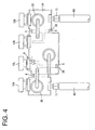
FIG. 4 is a plan view of a primary molded unit, -
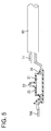
FIG. 5 is a section of the primary molded unit, -
FIG. 6 is a plan view of a cable surrounding portion before a sealing member is mounted, -
FIG. 7 is a plan view partly in section of the cable surrounding portion having the sealing member mounted thereon, -
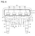
FIG. 8 is a plan view of a terminal box for solar cell module according to a second embodiment, and -
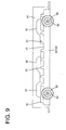
FIG. 9 is a rear view of the terminal box. - A first embodiment of the present invention is described with reference to
FIGS. 1 to 7 . A terminal box for solar cell module of this embodiment is to be attached to the underside of an unillustrated solar cell module in which a multitude of solar cells connected in series to one another are arranged, and includes a plurality ofterminal plates 10,bypass diodes 20 each bridged between twocorresponding terminal plates 10 and aresin portion 30 covering theterminal plates 10 and thebypass diodes 20. Theresin portion 30 is formed by ahousing 31 which is an outer envelope of this box. - Each
terminal plate 10 is formed to have a strip shape, for example, by cutting an electrically conductive metal plate, and fourterminal plates 10 are arranged side by side in a width direction. An unillustrated lead of a solar cell group is connected to one end portion of eachterminal plate 10.
Out of therespective terminal plates 10, two located at the opposite widthwise ends serve ascable connection terminals 10A each having acable 60 for taking an electromotive force out from the solar cell group connected to the other end portion thereof. Here, eachcable 60 is composed of acore 61 and aninsulation coating 62 surrounding thecore 61, thecore 61 is exposed at an end portion of thecable 60 by stripping off theinsulation coating 62, and a pair ofbarrel pieces 11 formed at the other end portion of thecable connection terminal 10A are crimped and connected to this exposedcore 61. An intermediate portion of thecable connection terminal 10A is formed to be wider than the one and the other end portions and aconnection hole 12, into which amain portion 21 of thebypass diode 20 is to be fitted, is formed to penetrate this intermediate portion (seeFIG. 3 ). - Out of the
respective terminal plates 10, two located between the bothcable connection terminals 10A serve asintermediate connection terminals intermediate connection terminal 10R (right one in the shown example) has themain body 21 of thebypass diode 20 supported thereon and the otherintermediate connection terminal 10L (left one in the shown example) has nomain body 21 supported thereon, but has the leading ends of connection pins 22 drawn out from themain bodies 21 supported on theterminal plates 10 at the opposite sides (cable connection terminal 10A and oneintermediate connection terminal 10R) connected thereto, for example, by soldering. - Similar to the
cable connection terminal 10A, aconnection hole 21, into which themain body 21 is to be fitted, is formed to penetrate the oneintermediate connection terminal 10R supporting themain body 21. Further, the oneintermediate connection terminal 10R is cut to form aspace portion 13 in the form of a slit in such a manner as to partition between themain body 21 and theconnection pin 22. Heat generated by thebypass diode 20 is transferred by way of thespace portion 13, thereby suppressing mutual thermal influence of thebypass diodes 20. - The one
intermediate connection terminal 10R has a largest surface area among all theterminal plates 10 to enhance a heat radiation property also at the time of heat generation by thebypass diodes 20. In contrast, the otherintermediate connection terminal 10L has a smallest surface area among all theterminal plates 10, thereby increasing the surface areas of the otherterminal plates 10 instead to improve space saving. - Each
bypass diode 20 is composed of themain body 21 in the form of a flat cylindrical block, and thebendable connection pin 22 drawn out from one end surface of themain body 21, and formed into a small package as a whole. Themain body 21 is such that a lateral side of a chip diode composed of a P-side area (anode-side area) and an N-side area (cathode-side area) is surrounded by a metal cylinder. A bottom part (anode-side area or cathode-side area) of the chip diode is held in contact with a bottom part of the cylinder to be electrically connected thereto, whereas insulating resin is filled between the cylinder excluding the bottom part and the chip diode. - The
connection pin 22 is bridged between theterminal plate 10 supporting themain body 21 and the terminal plate 10 (intermediate connection terminal terminal plate 10, a base end side thereof is electrically connected to the ceiling surface (cathode-side area or anode-side area) of the chip diode and a leading end side thereof is electrically connected to the adjacentterminal plate 10. - In the case of this embodiment, the
connection pin 22 of thebypass diode 20 bridged between thecable connection terminal 10A located at the left side in the shown example and the otherintermediate connection terminal 10L has an N-polarity, theconnection pin 22 of thebypass diode 20 bridged between thecable connection terminal 10A located at the right side in the shown example and the oneintermediate connection terminal 10R has a P-polarity, and theconnection pin 22 of thebypass diode 20 bridged between the oneintermediate connection terminal 10R and the otherintermediate connection terminal 10L has a P-polarity. Accordingly, each of the bothcable connection terminals 10A can support themain body 21 of thebypass diode 20 by reversing a direction of a PN-junction of one of therespective bypass diodes 20 and auxiliarily providing the otherintermediate connection terminal 10L. - The
respective terminal plates 10 andbypass diodes 20 are mold covered by theresin portion 30, wherefore thehousing 31 is integrally formed. Specifically, theresin portion 30 is in the form of a laterally long tube extending in a vertical direction and composed of atubular portion 14, in which one end portion of eachterminal plate 10 is located, and athinner portion 15 integral to and continuous with the other end of thetubular portion 14 and in the form of a thin layer deposited on therespective terminal plates 10, thebypass diodes 20 and the end portions of the cables 60 (seeFIGS. 1 and2 ). - The
tubular portion 14 includes a laterallylong opening 16, a plurality of leads corresponding to the solar cell groups are introduced into the opening 16 from a bottom side, and the respective introduced leads are connected to the one end portions of the correspondingterminal plates 10, for example, by soldering. An insulating resin material (potting material) is poured into theopening 16 of thetubular portion 14, and an unillustrated cover is mounted after the insulating resin material is poured. - The
thinner portion 15 includes aterminal surrounding portion 17 in the form of a thin layer deposited around theterminal plates 10,diode surrounding portions 18 in the form of thin layers deposited around thebypass diodes 20 andcable surrounding portions 19 in the form of thin layers deposited around the end portions of thecables 60. Theterminal surrounding portion 17 has a substantially flat shape extending along both the top surfaces and the undersides of theterminal plates 10. On the other hand, thediode surrounding portions 18 and thecable surrounding portions 19 have convex shapes projecting more upward than theterminal surrounding portion 17. - Each
cable surrounding portion 19 is formed to have a cylindrical shape surrounding the end portion of thecable 60 including thebarrel pieces 11 after being widened toward the end of thecable 60, and a pair ofprojections 19A of thecable surrounding portions 19 project in a draw-out direction of thecable 60 from the other end of thehousing 31. A stepped interlockingportion 9, with which a sealingmember 80 is to be engaged, is circumferentially formed in the outer circumferential surface of theprojection 19A, and apin removal hole 8 is formed at a side of theprojection 19A more toward the projecting end than the interlockingportion 9 upon removing a pin supporting thecable 60 at the time of molding thehousing 31. The sealingmember 80 is made of rubber such as silicon rubber and mounted on both theprojection 19A of thecable surrounding portion 19 and the end portion of thecable 60, and has a stepped lockingportion 81 corresponding to the interlockingportion 9 circumferentially formed on the inner circumferential surface thereof (seeFIG. 7 ). - Each
diode surrounding portion 18 has an outer shape in conformity with that of thebypass diode 20, and is composed of a firstdiode surrounding portion 18A extending along the circumferential surface and ceiling surface of themain body 21 of thebypass diode 20 and a seconddiode surrounding portion 18B extending along the circumferential surface and end surfaces of theconnection pin 22 of thebypass diode 20. The firstdiode surrounding portion 18A has a cylindrical shape standing up from theterminal surrounding portion 17, and the seconddiode surrounding portion 18B has a narrow and long cylindrical shape extending along the top surface of theterminal surrounding portion 17. The seconddiode surrounding portion 18B extends straight in the width direction from the circumferential surface of the firstdiode surrounding portion 18A. The upper surface of the seconddiode surrounding portion 18B is arranged at a position higher than that of the firstdiode surrounding portion 18A. One end of each of the firstdiode surrounding portions 18A located at the opposite widthwise ends is cut and joined with the other end of thetubular portion 14, and the other end thereof is joined with one end of thecable surrounding portion 19. - The
resin portion 30 is composed of aprimary resin layer 34 deposited on the terminal plates 10 (excluding the lead and a connected part to thecable 60 for eachcable connection terminal 10A) and thebypass diodes 20, and a secondary resin layer 35 placed on the outer side of theprimary resin layer 34, deposited on the connected parts of thecable connection terminals 10A and thecables 60 and including a surface which specifies an appearance configuration of thehousing 31. Theselayers 34, 35 are made of different resin materials. Theprimary resin layer 34 is thinner than the secondary resin layer 35, and both theprimary resin layer 34 and the secondary resin layer 35 have outer shapes in conformity with those of therespective terminal plates 10 andbypass diodes 20. When the surface shape of the secondary resin layer 35 is seen, the positions of thebypass diodes 20 and the like can be confirmed. - The
primary resin layer 34 is made of thermoplastic resin having good heat resistance such as polyphenylene sulfide (hereinafter, called "PPS"), and higher heat resistance is exhibited by containing glass fibers. In contrast, the secondary resin layer 35 is made of thermoplastic resin having good weather resistance and mechanical property such as polyphenylene ether (hereinafter, called "PPE"), and no glass fibers are contained therein. The PPS constituting theprimary resin layer 34 has a coefficient of linear expansion lower and more approximate to that of metal such as copper alloy constituting therespective terminal plates 10 and the connection pins 22 of thebypass diodes 20 than that of the PPE constituting the secondary resin layer 35. - Next, a method for producing the terminal box for solar cell module according to this embodiment and a method for mounting the terminal box on the solar cell module are described.
Upon producing the terminal box, chainedterminal plates 10 in which therespective terminal plates 10 are integrally connected viacarriers 6 are first prepared. A plurality ofcarriers 6 are bridged between the facing opposite edges of therespective terminal plates 10. Subsequently, themain bodies 21 of thebypass diodes 20 are press-fitted into the respective connection holes 12 of the bothcable connection terminals 10A and the oneintermediate connection terminal 10R and the leading ends of the connection pins 22 are placed on the top surfaces of the adjacent terminal plates 10 (intermediate connection terminals terminal plates 10 relative to each other are hindered by thecarriers 6, exertion of an excessive stress on the connected parts of the connection pins 22 and theterminal plates 10 can be avoided. - Subsequently, the
cores 61 of the end portions of thecables 60 are placed on the other end portions of thecable connection terminals 10A, thebarrel pieces 11 are crimped and connected to thecores 61 in this state, and thecable connection terminals 10A are connected to the end portions of the cables 60 (seeFIG. 3 ). Note that the sealingmembers 80 are mounted on the outer circumferential surfaces of thecables 60 in advance prior to connection to thecable connection terminals 10A (seeFIG. 6 ). - Subsequently, the above chained terminal unit is set in an unillustrated mold for primary molding and resin is filled into this mold. Then, the intermediate portions of the
respective terminal plates 10 excluding thecarriers 6 and the rectifying elements are covered by a thin layer of the resin, thereby forming the primary resin layer 34 (seeFIGS. 4 and5 ). At this time,cutouts 36 for exposing thecarriers 6 are formed to have three open sides in parts corresponding to thecarriers 6. - Subsequently, the
carriers 6 are cut and removed through thecutouts 36, thereby separating therespective terminal plates 10 from each other. After removing thecarriers 6, displacements of theterminal plates 10 relative to each other are hindered by theprimary resin layer 34. - Subsequently, the above primary molded unit is set in an unillustrated mold for secondary molding and resin is filled into this mold. Then, the secondary resin layer 35 is deposited on the outer side of the
primary resin layer 34 to form thethinner portion 15, and thetubular portion 14 is formed on one end of thethinner portion 15, whereby thehousing 30 is integrally formed (seeFIGS. 1 and2 ). At this time, the resin of the secondary resin layer 35 also covers thecutouts 36, which then disappear. Thecables 60 can be positioned and supported at specified height positions by being pressed from both above and below by unillustrated pins at the time of such secondary molding, whereas the pin removal holes 8 are left in theprojections 19A of thecable surrounding portions 19 by removing the pins. Note that an adhesive is applied to the outer circumferential surfaces of the end portions of thecables 60 prior to secondary molding and the end portions of thecables 60 and the secondary resin layer 35 are closely bonded via the adhesive after secondary molding. - Subsequently, the sealing
members 80 are pulled up toward thecable connection terminals 10A and retained and mounted on theresin portion 30 by the engagement of the lockingportions 81 and the interlocking portions 9 (seeFIG. 7 ). This prevents water penetration to clearances between thecable surrounding portions 19 and the end portions of thecables 60 to provide sealing in theresin portion 30. Further, when the sealingmembers 80 are mounted on theresin portion 30, the openings of the pin removal holes 8 are sealed by the sealingmembers 80. - Thereafter, the bottom surface of the
housing 31 is mounted on the solar cell module by an adhesive or the like. In the mounting process, the leads are pulled into theopening 16 of thetubular portion 14 and the leading ends of the leads are soldered to the one end portions of the correspondingterminal plates 10. Subsequently, insulating resin such as silicon resin is filled into theopening 16 and a cover is mounted on theopening 16. In this way, the mounting of the terminal box on the solar cell module is completed. - Since the
bypass diodes 20 reach very high temperatures when used, they may be damaged by heat of their own and their rectifying function may be disrupted. In this respect, according to this embodiment, heat generated by thebypass diodes 20 is satisfactorily released from the bottom surface of thethinner portion 15 toward the solar cell module and from the ceiling surface of thethinner portion 15 toward the atmosphere, wherefore a heat radiation property is good. - Further, since the
primary resin layer 34 is made of the PPS having higher heat resistance than the secondary resin layer 35, even if thebypass diodes 20 reach high temperatures, such a state can be coped with. In addition, since theprimary resin layer 34 has a coefficient of expansion more approximate to that of thebypass diodes 20 than the secondary resin layer 35, it can be avoided that loads acting on the connection pins 22 of thebypass diodes 20 become excessive due to thermal expansions of theprimary resin layer 34 and thebypass diodes 20. On the other hand, the secondary resin layer 35 that does not strongly require such properties can be made of the PPE and the PPE provides good weather resistance, wherefore the secondary resin layer 35 can bear exposure and use outdoors. - Since the
primary resin layer 34 contains the glass fibers, it has good heat resistance against heat generated by thebypass diodes 20. In contrast, since the secondary resin layer 35 contains no glass fibers, the box can avoid being subject to destruction or the like by an impact at the time of a fall. - Further, since the openings of the pin removal holes 8 are sealed by the sealing
members 80 that seal between thecables 60 and theresin portion 30 after thehousing 30 is molded, entrance of external matters into the pin removal holes 8 can be prevented. In this case, since it is not necessary to seal the pin removal holes 8 by separately applying potting or the like, operability can be improved and the construction can be simplified. - Furthermore, since the adhesive is interposed between the insulation coatings of the
cables 60 and theresin portion 30, formation of clearances between the insulation coatings and theresin portion 30 can be avoided, for example, even if thecables 60 become thinner due to long time use, wherefore a predetermined sealing property can be maintained for long periods. -
FIGS. 8 and9 show a second embodiment of the present invention. In the second embodiment, a multitude ofheat radiation fins 51 are integrally formed on a surface of athinner portion 15. The other construction is similar to the first embodiment and the construction similar to the first embodiment is identified by the same reference numerals and not repeatedly described. - The respective multitude of
fins 51 are in the form of narrow and long ribs extending in a direction parallel to a draw-out direction ofcables 60 and arranged at substantially regular intervals, and form a vertical stripe pattern as a whole. Further, therespective fins 51 are formed only on aterminal surrounding portion 17, but neither ondiode surrounding portions 18 nor oncable surrounding portions 19, and intersect with and are connected to the outer peripheries of thediode surrounding portions 18 and thecable surrounding portions 19. According to the second embodiment, a heat radiation property toward the atmosphere is further improved by theheat radiation fins 51. - The present invention is not limited to the embodiments described above and illustrated in the drawings. For example, the following modes are also included in the technical scope of the present invention.
- (1) The primary resin layer may be made of thermosetting resin such as epoxy resin or unsaturated polyester resin instead of the PPS.
- (2) In the second embodiment, the fins may also be formed on the diode surrounding portions or the cable surrounding portions.
- (3) The sealing members may be omitted. In this case, primer or the like may be provided between the insulation coatings of the cables and the resin portion surrounding them.
- (4) The bypass diodes are not limited to the package diodes as described above and bare chip diodes or the like may be used.
- (5) The terminal plates may include only two cable connection terminals and only one bypass diode may be formed to bridge between the two cable connection terminals.
- (6) The thinner portion may have a single layer structure by omitting the secondary resin layer.
- (7) The thinner portion may be formed only around the bypass diodes.
-
- 10
- terminal plate
- 15
- thinner portion
- 20
- bypass diode (rectifying element)
- 30
- resin portion
- 31
- housing
- 34
- primary resin layer
- 35
- secondary resin layer
- 51
- fin
- 60
- cable
- 80
- sealing member
Claims (10)
- A terminal box for solar cell module, comprising:a plurality of terminal plates electrically connected to a solar cell module,a bypass rectifying element at the time of a reverse load electrically connected to two corresponding ones of the respective terminal plates,a resin portion constituting a housing of the terminal box and mold-covering the respective terminal plates and the rectifying element, anda thinner portion formed in the resin portion and deposited on the rectifying element to have an outer shape in conformity with that of the rectifying element.
- A terminal box according to claim 1, wherein:the thinner portion includes a terminal surrounding portion deposited around the terminal plates and a diode surrounding portion deposited around the rectifying element, andthe diode surrounding portion has a convex shape projecting more than the terminal surrounding portion.
- A terminal box according to claim 2, wherein:the rectifying element includes a main body with a chip diode, and a connection pin drawn out from the main body to be connected to the terminal plate,the diode surrounding portion includes a first diode surrounding portion deposited around the main body and a second diode surrounding portion deposited around the terminal plate, andthe second diode surrounding portion extends from a circumferential surface of the first diode surrounding portion.
- A terminal box according to any one of claims 1 to 3, wherein:the resin portion includes a primary resin layer deposited on the respective terminal plates and the rectifying element and a secondary resin layer arranged on an outer side of the primary resin layer, andthe primary resin layer has higher heat resistance and a coefficient of expansion more approximate to that of the rectifying element than the secondary resin layer.
- A terminal box according to claim 4, wherein:the primary resin layer contains glass fibers, andthe secondary resin layer contains no glass fibers.
- A terminal box according to claim 4 or 5, wherein:the primary resin layer is made of polyphenylene sulfide, andthe secondary resin layer is made of polyphenylene ether.
- A terminal box according to any one of claims 4 to 6, wherein:an external connection cable drawn out to the outside from the housing is connected to the terminal plate, andthe secondary resin layer is deposited around a connected part of the terminal plate and the cable.
- A terminal box according to any one of claims 1 to 7, wherein heat radiation fins are formed on an outer surface of the resin portion.
- A terminal box according to any one of claims 1 to 8, wherein:an external connection cable drawn out to the outside from the housing is connected to the terminal plate,a sealing member for sealing between the cable and the resin portion in a watertight manner is mounted on the cable and the resin portion, andthe sealing member is so arranged as to seal an opening of a pin removal hole formed in the resin portion.
- A terminal box according to claim 9, wherein an adhesive is interposed between an insulation coating of the cable and the resin portion surrounding around the insulation coating.
Applications Claiming Priority (2)
| Application Number | Priority Date | Filing Date | Title |
|---|---|---|---|
| JP2009128242A JP5146406B2 (en) | 2009-05-27 | 2009-05-27 | Terminal box for solar cell module |
| PCT/JP2009/068096 WO2010137188A1 (en) | 2009-05-27 | 2009-10-21 | Terminal box for solar cell module |
Publications (2)
| Publication Number | Publication Date |
|---|---|
| EP2437308A1 true EP2437308A1 (en) | 2012-04-04 |
| EP2437308A4 EP2437308A4 (en) | 2014-01-08 |
Family
ID=43222324
Family Applications (1)
| Application Number | Title | Priority Date | Filing Date |
|---|---|---|---|
| EP09845249.3A Withdrawn EP2437308A4 (en) | 2009-05-27 | 2009-10-21 | Terminal box for solar cell module |
Country Status (5)
| Country | Link |
|---|---|
| US (1) | US8547685B2 (en) |
| EP (1) | EP2437308A4 (en) |
| JP (1) | JP5146406B2 (en) |
| CN (1) | CN102105996B (en) |
| WO (1) | WO2010137188A1 (en) |
Cited By (1)
| Publication number | Priority date | Publication date | Assignee | Title |
|---|---|---|---|---|
| EP3514949A1 (en) * | 2018-01-18 | 2019-07-24 | Zhejiang Renhe Photovoltaic Technology Co., Ltd. | Electrically conductive module of solar cell terminal box |
Families Citing this family (6)
| Publication number | Priority date | Publication date | Assignee | Title |
|---|---|---|---|---|
| JP5273075B2 (en) * | 2010-03-23 | 2013-08-28 | 住友電装株式会社 | Terminal box for solar cell module |
| JP2011199115A (en) * | 2010-03-23 | 2011-10-06 | Sumitomo Wiring Syst Ltd | Diode module and terminal box for solar cell module |
| EP2546932A3 (en) * | 2011-07-15 | 2015-06-24 | Hosiden Corporation | Terminal box and terminal box fixing arrangement |
| JP5729648B2 (en) * | 2011-10-13 | 2015-06-03 | ホシデン株式会社 | Terminal box for solar cell module |
| JP5962960B2 (en) * | 2012-03-01 | 2016-08-03 | 株式会社ジェイテクト | Waterproof structure of electronic unit |
| CN106685342B (en) * | 2017-03-10 | 2018-06-19 | 江苏通灵电器股份有限公司 | Chip low-voltage encapsulation junction box for solar power generation components and processing method thereof |
Family Cites Families (18)
| Publication number | Priority date | Publication date | Assignee | Title |
|---|---|---|---|---|
| JPH1126035A (en) * | 1997-07-04 | 1999-01-29 | Engel Kogyo Kk | Terminal box for solar cell module |
| JP3656391B2 (en) * | 1998-03-02 | 2005-06-08 | 三菱電機株式会社 | Solar cell module |
| JP3498945B2 (en) | 1999-09-01 | 2004-02-23 | オーナンバ株式会社 | Terminal box device for connecting solar cell modules |
| JP2004134717A (en) * | 2002-10-10 | 2004-04-30 | Sumisho Metalex Corp | Terminal box for solar cell module, and its forming method |
| JP4232150B2 (en) | 2003-06-27 | 2009-03-04 | 三菱電機株式会社 | Terminal box |
| JP4681806B2 (en) * | 2003-12-19 | 2011-05-11 | キヤノン株式会社 | Solar cell module |
| JP2006013145A (en) * | 2004-06-25 | 2006-01-12 | Sumitomo Wiring Syst Ltd | Terminal box for solar cell module |
| JP3767618B2 (en) * | 2004-08-19 | 2006-04-19 | 住友電装株式会社 | Terminal box for solar cell module |
| JP2006059990A (en) * | 2004-08-19 | 2006-03-02 | Sumitomo Wiring Syst Ltd | Terminal box for solar cell module |
| JP5060786B2 (en) * | 2004-11-25 | 2012-10-31 | 株式会社三社電機製作所 | Connector for solar cell module |
| JP2006165017A (en) * | 2004-12-02 | 2006-06-22 | Sumitomo Wiring Syst Ltd | Terminal box for solar cell module |
| JP2006286996A (en) * | 2005-04-01 | 2006-10-19 | Oonanba Kk | Terminal box for solar panel |
| JP3852710B1 (en) * | 2005-11-01 | 2006-12-06 | 住友電装株式会社 | Terminal box for solar cell module |
| JP3852711B1 (en) * | 2005-11-09 | 2006-12-06 | 住友電装株式会社 | Terminal box for solar cell module |
| CN100511717C (en) * | 2006-05-19 | 2009-07-08 | 上海行田电产有限公司 | Terminal box for solar battery assembly |
| JP2007311714A (en) * | 2006-05-22 | 2007-11-29 | Yunikon Denshi Kk | Diode module, connector for solar cell module, and its manufacturing method |
| WO2008095670A1 (en) * | 2007-02-05 | 2008-08-14 | Phoenix Contact Gmbh & Co. Kg | Junction box and connecting box for a solar module |
| US8139373B2 (en) * | 2007-07-18 | 2012-03-20 | Mitsubishi Electric Corporation | Terminal box |
-
2009
- 2009-05-27 JP JP2009128242A patent/JP5146406B2/en not_active Expired - Fee Related
- 2009-10-21 US US12/993,996 patent/US8547685B2/en not_active Expired - Fee Related
- 2009-10-21 WO PCT/JP2009/068096 patent/WO2010137188A1/en not_active Ceased
- 2009-10-21 EP EP09845249.3A patent/EP2437308A4/en not_active Withdrawn
- 2009-10-21 CN CN2009801292979A patent/CN102105996B/en not_active Expired - Fee Related
Cited By (1)
| Publication number | Priority date | Publication date | Assignee | Title |
|---|---|---|---|---|
| EP3514949A1 (en) * | 2018-01-18 | 2019-07-24 | Zhejiang Renhe Photovoltaic Technology Co., Ltd. | Electrically conductive module of solar cell terminal box |
Also Published As
| Publication number | Publication date |
|---|---|
| EP2437308A4 (en) | 2014-01-08 |
| WO2010137188A1 (en) | 2010-12-02 |
| JP2010278162A (en) | 2010-12-09 |
| JP5146406B2 (en) | 2013-02-20 |
| US8547685B2 (en) | 2013-10-01 |
| CN102105996B (en) | 2013-07-17 |
| US20120057304A1 (en) | 2012-03-08 |
| CN102105996A (en) | 2011-06-22 |
Similar Documents
| Publication | Publication Date | Title |
|---|---|---|
| US7906721B2 (en) | Solar cell module connector | |
| US6655987B2 (en) | Terminal box apparatus for solar cell module | |
| US8547685B2 (en) | Terminal box for solar cell module | |
| US7920385B2 (en) | Terminal box for solar cell module | |
| US6828503B2 (en) | Terminal box device for a solar cell module and a connecting method for a terminal box device | |
| US8512050B2 (en) | Solar panel junction box | |
| US7723609B2 (en) | Terminal box for solar battery module | |
| US8979597B2 (en) | Leadframe having selectively removable bridges between terminals and contacts | |
| US8184440B2 (en) | Electronic apparatus having an encapsulating layer within and outside of a molded frame overlying a connection arrangement on a circuit board | |
| WO2009129405A2 (en) | Solar panel junction box | |
| CN105659440A (en) | Connection arrangement for connecting at least one voltage source and/or voltage sink in form of cell to external electrical component and electrical arrangement comprising connection arrangement | |
| JP5487405B2 (en) | connector | |
| EP2530733A1 (en) | Terminal box for solar cell module, and solar cell module | |
| US8737042B2 (en) | Terminal box for use with solar cell module | |
| US10305422B2 (en) | Solar cell module and solar cell module manufacturing method | |
| JP2006165017A (en) | Terminal box for solar cell module | |
| WO2010052207A2 (en) | Connecting device for a photovoltaic solar module | |
| CN116614078A (en) | Photovoltaic modules and junction boxes for photovoltaic modules | |
| WO2010052210A2 (en) | Connecting device for a photovoltaic solar module | |
| JP2005236333A (en) | Terminal box equipment for solar cell module | |
| JP2006135246A (en) | Terminal box for solar cell module | |
| JP2006179685A (en) | Terminal box for solar cell module | |
| WO2011118069A1 (en) | Diode module and terminal box for solar cell module |
Legal Events
| Date | Code | Title | Description |
|---|---|---|---|
| PUAI | Public reference made under article 153(3) epc to a published international application that has entered the european phase |
Free format text: ORIGINAL CODE: 0009012 |
|
| 17P | Request for examination filed |
Effective date: 20101209 |
|
| AK | Designated contracting states |
Kind code of ref document: A1 Designated state(s): AT BE BG CH CY CZ DE DK EE ES FI FR GB GR HR HU IE IS IT LI LT LU LV MC MK MT NL NO PL PT RO SE SI SK SM TR |
|
| DAX | Request for extension of the european patent (deleted) | ||
| A4 | Supplementary search report drawn up and despatched |
Effective date: 20131210 |
|
| RIC1 | Information provided on ipc code assigned before grant |
Ipc: H01L 31/048 20060101ALI20131204BHEP Ipc: H01L 31/042 20060101AFI20131204BHEP Ipc: H01R 13/66 20060101ALI20131204BHEP Ipc: H01R 9/24 20060101ALI20131204BHEP |
|
| STAA | Information on the status of an ep patent application or granted ep patent |
Free format text: STATUS: THE APPLICATION IS DEEMED TO BE WITHDRAWN |
|
| 18D | Application deemed to be withdrawn |
Effective date: 20140722 |