EP2437293A2 - Semiconductor cooling apparatus - Google Patents
Semiconductor cooling apparatus Download PDFInfo
- Publication number
- EP2437293A2 EP2437293A2 EP11177471A EP11177471A EP2437293A2 EP 2437293 A2 EP2437293 A2 EP 2437293A2 EP 11177471 A EP11177471 A EP 11177471A EP 11177471 A EP11177471 A EP 11177471A EP 2437293 A2 EP2437293 A2 EP 2437293A2
- Authority
- EP
- European Patent Office
- Prior art keywords
- cooling
- semiconductor
- coolant
- cooling apparatus
- elements
- Prior art date
- Legal status (The legal status is an assumption and is not a legal conclusion. Google has not performed a legal analysis and makes no representation as to the accuracy of the status listed.)
- Withdrawn
Links
Images


Classifications
-
- H—ELECTRICITY
- H10—SEMICONDUCTOR DEVICES; ELECTRIC SOLID-STATE DEVICES NOT OTHERWISE PROVIDED FOR
- H10W—GENERIC PACKAGES, INTERCONNECTIONS, CONNECTORS OR OTHER CONSTRUCTIONAL DETAILS OF DEVICES COVERED BY CLASS H10
- H10W40/00—Arrangements for thermal protection or thermal control
- H10W40/40—Arrangements for thermal protection or thermal control involving heat exchange by flowing fluids
- H10W40/47—Arrangements for thermal protection or thermal control involving heat exchange by flowing fluids by flowing liquids, e.g. forced water cooling
-
- H—ELECTRICITY
- H10—SEMICONDUCTOR DEVICES; ELECTRIC SOLID-STATE DEVICES NOT OTHERWISE PROVIDED FOR
- H10W—GENERIC PACKAGES, INTERCONNECTIONS, CONNECTORS OR OTHER CONSTRUCTIONAL DETAILS OF DEVICES COVERED BY CLASS H10
- H10W40/00—Arrangements for thermal protection or thermal control
- H10W40/20—Arrangements for cooling
- H10W40/25—Arrangements for cooling characterised by their materials
- H10W40/255—Arrangements for cooling characterised by their materials having a laminate or multilayered structure, e.g. direct bond copper [DBC] ceramic substrates
-
- H—ELECTRICITY
- H10—SEMICONDUCTOR DEVICES; ELECTRIC SOLID-STATE DEVICES NOT OTHERWISE PROVIDED FOR
- H10W—GENERIC PACKAGES, INTERCONNECTIONS, CONNECTORS OR OTHER CONSTRUCTIONAL DETAILS OF DEVICES COVERED BY CLASS H10
- H10W40/00—Arrangements for thermal protection or thermal control
- H10W40/70—Fillings or auxiliary members in containers or in encapsulations for thermal protection or control
- H10W40/77—Auxiliary members characterised by their shape
- H10W40/774—Pistons, e.g. spring-loaded members
-
- H—ELECTRICITY
- H10—SEMICONDUCTOR DEVICES; ELECTRIC SOLID-STATE DEVICES NOT OTHERWISE PROVIDED FOR
- H10W—GENERIC PACKAGES, INTERCONNECTIONS, CONNECTORS OR OTHER CONSTRUCTIONAL DETAILS OF DEVICES COVERED BY CLASS H10
- H10W40/00—Arrangements for thermal protection or thermal control
- H10W40/60—Securing means for detachable heating or cooling arrangements, e.g. clamps
- H10W40/641—Snap-on arrangements, e.g. clips
Definitions
- a flat aluminum brazed monolithic cooling apparatus can be used with highly conformal low thermal performance heat spreaders, such as a gap pad or gap filler material, to accommodate vertical height variations in semiconductors and individual variations in planarity with respect to the cooling apparatus surface. After the individual semiconductors are attached to an array, the semiconductor height variations can be mapped for the entire array in order to select custom heat spreaders for each semiconductor element.
- This solution generally, is effective for planar arrays, but, generally, this solution is not effective for semiconductor arrays with various vertical height variations due to the inefficiency of the heat spreaders and the difficulties of accurately mapping and fitting the custom heat spreaders.
- One approach to a semiconductor cooling apparatus includes a monolithic array of cooling elements.
- Each cooling element is configured to thermally couple to a respective semiconductor element of an array of semiconductor elements. At least two of the semiconductor elements have a different height and each cooling element independently flexes to conform to the height of the respective semiconductor element.
- Another approach to a semiconductor cooling apparatus includes a means for cooling semiconductor elements and a means for flexibly conforming each means for cooling to a respective height of a respective semiconductor element.
- the means for cooling is arranged in a monolithic array.
- Each means for cooling is thermally coupled to a respective semiconductor element of an array of semiconductor elements. At least two of the semiconductor elements have a different height.
- each cooling element further includes a coolant supply manifold and a coolant return manifold.
- the coolant supply manifold is flexibly coupled to a coolant supply line.
- the coolant return manifold is flexibly coupled to a coolant return line.
- the coolant supply manifold and the coolant return manifold are substantially wrap-around a part of the respective cooling element.
- the coolant supply manifold and the coolant return manifold flex independent of the monolithic array of cooling elements.
- each cooling element is formable through a bonding process to form a monolithic structure.
- the bonding includes diffusion bonding, adhesive bonding, and/or brazing.
- each cooling element is bonded together to form the monolithic array.
- the semiconductor cooling apparatus further includes a coolant chilling apparatus and a coolant pump.
- the coolant chilling apparatus is connected to the coolant supply line and the coolant return line and configured to chill coolant.
- the coolant pump is configured to pump the coolant between the coolant chilling apparatus and the array of cooling elements.
- the coolant comprising a liquid coolant, and/or a gaseous coolant.
- the coolant is supplied to each cooling element in parallel.
- each cooling element reduces a thermal resistance interface between the cooling element and the respective semiconductor element.
- the semiconductor cooling apparatus further includes a plurality of spring clips.
- Each spring clip is configured to couple the respective cooling element in the array of cooling elements to its respective semiconductor element.
- the semiconductor cooling apparatus includes aluminum, copper, and/or stainless steel.
- the semiconductor cooling apparatus further includes a means for coupling the means for cooling to the respective semiconductor element.
- FIG. 1 is a block diagram of an exemplary semiconductor cooling apparatus and semiconductor array
- FIG. 2 is an illustration of another exemplary semiconductor cooling apparatus
- FIG. 3 is an illustration of internal parts of another exemplary cooling element
- FIG. 4 is a view of another exemplary cooling element
- FIG. 5A is an illustration of another exemplary semiconductor cooling apparatus
- FIG. 5B is an illustration of an exemplary array of semiconductor elements
- FIG. 5C is an illustration of another exemplary semiconductor cooling apparatus mounted on an exemplary array of semiconductor elements
- FIG. 6 is an illustration of another exemplary semiconductor cooling apparatus
- FIG. 7 is an exploded view of layers of an exemplary unassembled semiconductor cooling apparatus.
- FIG. 8 is a cross sectional view of another exemplary semiconductor cooling apparatus.
- Semiconductor elements such as a ball grid array (BGA) can be used as part of aerospace sensor architectures and/or other semiconductor architectures.
- BGA ball grid array
- each of the semiconductor elements is soldered to a primary circuit board (e.g., motherboard, array, etc.) creating the semiconductor array. Due to the size, spacing, and thermal properties of the semiconductor elements on the array, a semiconductor cooling apparatus is needed to quickly and efficiently transfer heat from the array.
- each element in the semiconductor array can have different stackups (also referred to as vertical heights of the elements) making it difficult to effectively transfer heat from each stack.
- the semiconductor cooling apparatus includes a monolithic array of cooling elements, where each cooling element can be configured to thermally couple to a respective semiconductor element (stack-up) of an array of semiconductor elements.
- each cooling element can independently flex to conform to the height of the respective semiconductor element (e.g., a math coprocessor is 0.02 inches high and a video processor is 0.04 inches high, an input/output processor is 0.023 inches high and an encryption processor is 0.034 inches high, etc.), thereby increasing the thermal transfer between the semiconductor element and the cooling element.
- the semiconductor cooling apparatus (e.g., a conformal foil cold wall, a monolithic flexible sheet, etc.) includes multiple cooling elements (e.g., coolers, cooling areas, etc.) sized so that there is one cooling element per semiconductor element (e.g., a BGA heat spreader, a processor, etc.).
- Coolant e.g., liquid, air, etc.
- flexible runners e.g., one inlet and one outlet
- the semiconductor cooling apparatus can be fabricated by diffusion bonding multiple foil layers providing a thin single piece or monolithic, flexible flat architecture.
- the semiconductor cooling apparatus can be made of copper and/or copper alloys, thereby improving thermal performance and allowing the semiconductor cooling apparatus to be deformed slightly at strategic points if needed to conform to 2D architectures.
- the semiconductor cooling apparatus as described herein can advantageously solve this thermal design problem by combining diffusion bonding fabrication that creates thin highly planar microchannel assemblies with flexible elements that integrate both structural and hydraulic functions.
- the architecture of the semiconductor cooling apparatus e.g., copper foil, copper alloy, etc.
- FIG. 1 is a block diagram 100 of an exemplary semiconductor cooling apparatus 110 and semiconductor array 120 (e.g., ball grid array (BGA), computer motherboard, etc.).
- the semiconductor cooling apparatus 110 includes a monolithic array of cooling elements 112, 114, 116, and 118 (e.g., a single formed sheet of cooling elements, a homogenous array of cooling elements, a heterogeneous array of cooling elements, etc.).
- the semiconductor array 120 includes semiconductor elements of various heights, widths, and lengths 122, 124, 126, and 128.
- Each cooling element 112, 114, 116, and 118 of the semiconductor cooling apparatus 110 is configured to thermally couple (e.g., positioned near each other to enable thermal transfer, positioned near each other to maximize thermal transfer, etc.) to the respective semiconductor element 122, 124, 126, and 128 of the array of semiconductor elements 120.
- each cooling element 112, 114, 116, and 118 independently flexes to conform to the height of the respective semiconductor element 122, 124, 126, and 128, respectively (e.g., the cooling elements flex from 0.001 to 0.009 inches, the cooling elements flex from 0.01 to 0.09 inches, etc.).
- the cooling element 112 flexes independently from the other cooling elements 114, 116, and 118 to conform to the height of the semiconductor element 122.
- each cooling element advantageously increases the heat transfer between the semiconductor element and the cooling element, thereby extending the life of the semiconductor element by promoting proper cooling of the semiconductor element.
- the independent flexibility of each cooling element and/or the monolithic design of the semiconductor cooling apparatus advantageously reduces the installation time and cost by removing any needed individual customizations, thereby decreasing the overall cost of the devices associated with the semiconductor element while increasing the heat transfer.
- each cooling element 112, 114, 116, and 118 reduces a thermal resistance interface between the cooling element 112, 114, 116, and 118 and the respective semiconductor element 122, 124, 126, and 128.
- the cooling element 112 flexes 0.003 inches to be 0.001 inches from the respective semiconductor element 122
- the cooling element 114 flexes 0.002 inches to be 0.001 inches from the respective semiconductor element 124.
- each cooling element 112, 114, 116, and 118 advantageously enables the thermal resistance interface to be reduced (e.g., reduced thermal penalty from 20° C to 10° C; reduced thermal penalty from 8° C to 3.2° C, etc.), thereby increasing the efficiency of the semiconductor cooling apparatus and increasing the life of the semiconductor elements.
- the semiconductor cooling apparatus can be produced using aluminum, copper, stainless steel, and/or material with high heat transfer (e.g., Glidcop available from SCM Metal Products, Inc., a copper alloy, etc.).
- material with high heat transfer e.g., Glidcop available from SCM Metal Products, Inc., a copper alloy, etc.
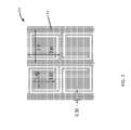
- FIG. 2 is an illustration of another exemplary semiconductor cooling apparatus 200.
- the semiconductor cooling apparatus includes four cooling elements (e.g., cooling element 214). As illustrated in FIG. 2 , each cooling element has outside dimensions of two inches by two inches and internal dimensions of 1.48 inches by 1.80 inches.
- the semiconductor cooling apparatus 200 illustrated in FIG. 2 can include top and bottom layers (not shown) to enclose the cooling elements (e.g., to prevent contamination of the semiconductor cooling apparatus 200 and/or parts therein, for ease of installation of the semiconductor cooling apparatus, etc.).
- FIG. 2 illustrates four cooling elements in the semiconductor cooling apparatus 200
- the semiconductor cooling apparatus 200 can include any number of cooling elements as needed to provide heat transfer of the semiconductor array (e.g., sixteen, twenty, forty, etc.).
- the cooling elements in the semiconductor cooling apparatus 200 can be in one or more shapes and/or dimensions.
- the semiconductor cooling apparatus includes four 2x2 inch cooling elements and eight 2x3 inch cooling elements.
- the semiconductor cooling apparatus includes four sets of four 3x3 inch cooling elements with two inch blank spaces between the sets of cooling elements.
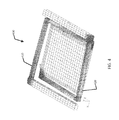
- FIG. 3 is an illustration of internal cavities (channels) of another exemplary cooling element 300.
- the cooling element 300 includes a coolant supply manifold 310, a coolant return manifold 320, and a mounting device 330.
- the coolant supply manifold 310 is flexibly coupled to a coolant supply line (not shown).
- the coolant return manifold 320 is flexibly coupled to a coolant return line (not shown).
- the mounting device 330 is utilized to mount the cooling element 300 on a semiconductor element (e.g., mounting hold for a spring clip, nut and bolt assembly, etc.).
- the coolant supply manifold 310 and the coolant return manifold 320 substantially wrap-around a part of the cooling element 300.
- the wrap-around of the manifolds 310 and 320 advantageously enables the cooling element 300 to individually flex (like a slinky) based on the height of the respective semiconductor element, thereby increasing the heat transfer between the cooling element and the semiconductor element, thereby extending the life of the semiconductor element.
- FIG. 4 is a view of another exemplary cooling element 400.
- the cooling element 400 includes a coolant supply manifold 410 and a coolant return manifold 420.
- the coolant supply manifold 410 and the coolant return manifold 420 flex independent of the monolithic array of cooling elements (e.g., semiconductor cooling apparatus 110 of FIG. 1 ).
- the wrapping-around of the coolant supply manifold 410 and the coolant return manifold 420 advantageously enables the cooling element 400 to flex in 3-dimensions (i.e., the x, y, and z planes).
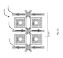
- FIG. 5A is an illustration of another exemplary semiconductor cooling apparatus 500a.
- the semiconductor cooling apparatus 500a includes coolant supply lines 512a and 516a, a coolant return line 514a, and cooling elements 522a, 524a, 526a, and 528a.
- the coolant supply line 512a supplies coolant to the cooling elements 522a and 526a from a coolant chilling apparatus (not shown).
- the coolant supply line 516a supplies coolant to the cooling elements 524a and 528a from the coolant chilling apparatus.
- the coolant return line 514a returns coolant from the cooling elements 522a, 524a, 526a, and 528a to the coolant chilling apparatus.
- FIG. 5B is an illustration of an exemplary array of semiconductor elements 500b.
- the array of semiconductor elements 500b includes semiconductor elements 532b, 534b, 536b, and 538b.
- each semiconductor element 532b, 534b, 536b, and 538b includes a mounting tab 542b, 544b, 546b, and 548b, respectively, for securing a cooling element to the semiconductor element (e.g., via a spring clip, via a nut, etc.).
- FIG. 5C is an illustration of another exemplary semiconductor cooling apparatus 510c mounted on an exemplary array of semiconductor elements 530c.
- a spring clip e.g., 512c
- each cooling element attaches to the respective semiconductor element, thereby securing the semiconductor cooling apparatus and parts thereof (i.e., the cooling elements) to the array of semiconductor elements 530c and respective parts thereof (i.e., the semiconductor elements).
- FIG. 6 is an illustration of another exemplary semiconductor cooling apparatus 600.
- the semiconductor cooling apparatus includes an array of cooling elements 610, a coolant chilling apparatus 650, and a coolant pump 660.
- the coolant chilling apparatus 650 is connected to one or more coolant supply lines and one or more coolant return lines and is configured to chill coolant.
- the coolant pump 660 is configured to pump the coolant between the coolant chilling apparatus 650 and the array of cooling elements 610.
- the coolant includes a liquid coolant (e.g., oil, water, etc.), a gaseous coolant and/or any other type of coolant.
- a liquid coolant e.g., oil, water, etc.
- a gaseous coolant e.g., water, etc.
- the coolant is supplied to each cooling element in parallel.
- the one or more coolant supply lines supply the chilled coolant to the array of cooling elements 610 in parallel, thereby advantageously enabling the chilled coolant to be provided to each cooling element while chilled and extending the life of the cooling elements.
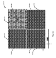
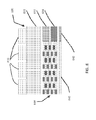
- FIG. 7 is an exploded view of layers of an exemplary unassembled semiconductor cooling apparatus 700.
- the unassembled semiconductor cooling apparatus 700 includes a plurality of layers including cap layers 710 and 718 and internal layers 711, 712, 713, 714, 715, 716, and 717.
- FIG. 7 illustrates the unassembled semiconductor cooling apparatus 700 having two cap layers and seven internal layers
- the unassembled semiconductor cooling apparatus can include any number of layers (e.g., two cap layers and one internal layer, four cap layers and ten internal layers, etc.).
- each cooling element is formable through a bonding process to form a monolithic structure.
- the bonding includes diffusion bonding, adhesive bonding, brazing, and/or any other type of bonding mechanism.
- each cooling element is bonded together to form the monolithic array.
- FIG. 8 is a cross sectional view of another exemplary semiconductor cooling apparatus 800 and an array of semiconductor elements 810.
- the semiconductor cooling apparatus 800 includes a facesheet 820 (i.e., a cap layer), a plurality of coolant channels 830b, a coolant supply channel 832b, a coolant return channel 834b, a cap foil 840b (i.e., a cap layer), and an inlet/outlet port 842b in the cap foil 840b for the coolant supply channel 832b and the coolant return channel 824b.
- Comprise, include, and/or plural forms of each are open ended and include the listed parts and can include additional parts that are not listed. And/or is open ended and includes one or more of the listed parts and combinations of the listed parts.
Landscapes
- Cooling Or The Like Of Semiconductors Or Solid State Devices (AREA)
Abstract
Description
- A flat aluminum brazed monolithic cooling apparatus can be used with highly conformal low thermal performance heat spreaders, such as a gap pad or gap filler material, to accommodate vertical height variations in semiconductors and individual variations in planarity with respect to the cooling apparatus surface. After the individual semiconductors are attached to an array, the semiconductor height variations can be mapped for the entire array in order to select custom heat spreaders for each semiconductor element. This solution, generally, is effective for planar arrays, but, generally, this solution is not effective for semiconductor arrays with various vertical height variations due to the inefficiency of the heat spreaders and the difficulties of accurately mapping and fitting the custom heat spreaders.
- Thus, a need exists in the art for a semiconductor cooling apparatus with the features as described herein.
- One approach to a semiconductor cooling apparatus includes a monolithic array of cooling elements. Each cooling element is configured to thermally couple to a respective semiconductor element of an array of semiconductor elements. At least two of the semiconductor elements have a different height and each cooling element independently flexes to conform to the height of the respective semiconductor element.
- Another approach to a semiconductor cooling apparatus includes a means for cooling semiconductor elements and a means for flexibly conforming each means for cooling to a respective height of a respective semiconductor element. The means for cooling is arranged in a monolithic array. Each means for cooling is thermally coupled to a respective semiconductor element of an array of semiconductor elements. At least two of the semiconductor elements have a different height.
- Any of the approaches described herein can include one or more of the following examples.
- In some examples, each cooling element further includes a coolant supply manifold and a coolant return manifold. The coolant supply manifold is flexibly coupled to a coolant supply line. The coolant return manifold is flexibly coupled to a coolant return line.
- In other examples, the coolant supply manifold and the coolant return manifold are substantially wrap-around a part of the respective cooling element.
- In some examples, the coolant supply manifold and the coolant return manifold flex independent of the monolithic array of cooling elements.
- In other examples, each cooling element is formable through a bonding process to form a monolithic structure.
- In some examples, the bonding includes diffusion bonding, adhesive bonding, and/or brazing.
- In other examples, each cooling element is bonded together to form the monolithic array.
- In some examples, the semiconductor cooling apparatus further includes a coolant chilling apparatus and a coolant pump. The coolant chilling apparatus is connected to the coolant supply line and the coolant return line and configured to chill coolant. The coolant pump is configured to pump the coolant between the coolant chilling apparatus and the array of cooling elements.
- In other examples, the coolant comprising a liquid coolant, and/or a gaseous coolant.
- In some examples, the coolant is supplied to each cooling element in parallel.
- In other examples, the flexing of each cooling element reduces a thermal resistance interface between the cooling element and the respective semiconductor element.
- In some examples, the semiconductor cooling apparatus further includes a plurality of spring clips. Each spring clip is configured to couple the respective cooling element in the array of cooling elements to its respective semiconductor element.
- In other examples, the semiconductor cooling apparatus includes aluminum, copper, and/or stainless steel.
- In some examples, the semiconductor cooling apparatus further includes a means for coupling the means for cooling to the respective semiconductor element.
- The foregoing and other objects, features and advantages will be apparent from the following more particular description of the embodiments, as illustrated in the accompanying drawings in which like reference characters refer to the same parts throughout the different views. The drawings are not necessarily to scale, emphasis instead being placed upon illustrating the principles of the embodiments.
-
FIG. 1 is a block diagram of an exemplary semiconductor cooling apparatus and semiconductor array; -
FIG. 2 is an illustration of another exemplary semiconductor cooling apparatus; -
FIG. 3 is an illustration of internal parts of another exemplary cooling element; -
FIG. 4 is a view of another exemplary cooling element; -
FIG. 5A is an illustration of another exemplary semiconductor cooling apparatus -
FIG. 5B is an illustration of an exemplary array of semiconductor elements; -
FIG. 5C is an illustration of another exemplary semiconductor cooling apparatus mounted on an exemplary array of semiconductor elements; -
FIG. 6 is an illustration of another exemplary semiconductor cooling apparatus; -
FIG. 7 is an exploded view of layers of an exemplary unassembled semiconductor cooling apparatus; and -
FIG. 8 is a cross sectional view of another exemplary semiconductor cooling apparatus. - Semiconductor elements, such as a ball grid array (BGA), can be used as part of aerospace sensor architectures and/or other semiconductor architectures. In most instances, each of the semiconductor elements is soldered to a primary circuit board (e.g., motherboard, array, etc.) creating the semiconductor array. Due to the size, spacing, and thermal properties of the semiconductor elements on the array, a semiconductor cooling apparatus is needed to quickly and efficiently transfer heat from the array. However, each element in the semiconductor array can have different stackups (also referred to as vertical heights of the elements) making it difficult to effectively transfer heat from each stack. Thus, the semiconductor cooling apparatus, as described herein, includes a monolithic array of cooling elements, where each cooling element can be configured to thermally couple to a respective semiconductor element (stack-up) of an array of semiconductor elements. Advantageously, each cooling element can independently flex to conform to the height of the respective semiconductor element (e.g., a math coprocessor is 0.02 inches high and a video processor is 0.04 inches high, an input/output processor is 0.023 inches high and an encryption processor is 0.034 inches high, etc.), thereby increasing the thermal transfer between the semiconductor element and the cooling element.
- As a general overview of the semiconductor cooling apparatus, the semiconductor cooling apparatus (e.g., a conformal foil cold wall, a monolithic flexible sheet, etc.) includes multiple cooling elements (e.g., coolers, cooling areas, etc.) sized so that there is one cooling element per semiconductor element (e.g., a BGA heat spreader, a processor, etc.). Coolant (e.g., liquid, air, etc.) flows into and out of the cooling element via flexible runners (e.g., one inlet and one outlet) that connect the cooling element to the main manifold channels. Each cooling element can, therefore, adapt to the vertical height and planarity variations of the semiconductor elements by way of the flexible runners.
- The semiconductor cooling apparatus can be fabricated by diffusion bonding multiple foil layers providing a thin single piece or monolithic, flexible flat architecture. The semiconductor cooling apparatus can be made of copper and/or copper alloys, thereby improving thermal performance and allowing the semiconductor cooling apparatus to be deformed slightly at strategic points if needed to conform to 2D architectures.
- Large arrays of semiconductor elements present a unique thermal design problem due to the large size of such arrays and large variations in the components utilized in such arrays. The semiconductor cooling apparatus as described herein can advantageously solve this thermal design problem by combining diffusion bonding fabrication that creates thin highly planar microchannel assemblies with flexible elements that integrate both structural and hydraulic functions. The architecture of the semiconductor cooling apparatus (e.g., copper foil, copper alloy, etc.) can be thin enough to be strategically deformed along the reinforced main manifolds (e.g., coolant supply manifold, coolant return manifold, etc.) in order to support faceted flat architectures consisting of 2 planar elements joined at a shallow angle=(i.e., enable each cooling element to flex independently for the respective semiconductor element).
-
FIG. 1 is a block diagram 100 of an exemplary semiconductor cooling apparatus 110 and semiconductor array 120 (e.g., ball grid array (BGA), computer motherboard, etc.). The semiconductor cooling apparatus 110 includes a monolithic array of cooling elements 112, 114, 116, and 118 (e.g., a single formed sheet of cooling elements, a homogenous array of cooling elements, a heterogeneous array of cooling elements, etc.). The semiconductor array 120 includes semiconductor elements of various heights, widths, and lengths 122, 124, 126, and 128. Each cooling element 112, 114, 116, and 118 of the semiconductor cooling apparatus 110 is configured to thermally couple (e.g., positioned near each other to enable thermal transfer, positioned near each other to maximize thermal transfer, etc.) to the respective semiconductor element 122, 124, 126, and 128 of the array of semiconductor elements 120. - As illustrated in
FIG. 1 , at least two of the semiconductor elements 122, 124, 126, and 128 have a different height (e.g., with respect to the top of the semiconductor mounting surface, with respect to the bottom of the semiconductor cooling apparatus 110, with respect to each other, etc.). In operation, each cooling element 112, 114, 116, and 118 independently flexes to conform to the height of the respective semiconductor element 122, 124, 126, and 128, respectively (e.g., the cooling elements flex from 0.001 to 0.009 inches, the cooling elements flex from 0.01 to 0.09 inches, etc.). For example, the cooling element 112 flexes independently from the other cooling elements 114, 116, and 118 to conform to the height of the semiconductor element 122. - The independent flexibility of each cooling element advantageously increases the heat transfer between the semiconductor element and the cooling element, thereby extending the life of the semiconductor element by promoting proper cooling of the semiconductor element. The independent flexibility of each cooling element and/or the monolithic design of the semiconductor cooling apparatus advantageously reduces the installation time and cost by removing any needed individual customizations, thereby decreasing the overall cost of the devices associated with the semiconductor element while increasing the heat transfer.
- In some examples, the flexible properties of each cooling element 112, 114, 116, and 118 reduces a thermal resistance interface between the cooling element 112, 114, 116, and 118 and the respective semiconductor element 122, 124, 126, and 128. For example, the cooling element 112 flexes 0.003 inches to be 0.001 inches from the respective semiconductor element 122, and the cooling element 114 flexes 0.002 inches to be 0.001 inches from the respective semiconductor element 124. The independent flexibility of each cooling element 112, 114, 116, and 118 advantageously enables the thermal resistance interface to be reduced (e.g., reduced thermal penalty from 20° C to 10° C; reduced thermal penalty from 8° C to 3.2° C, etc.), thereby increasing the efficiency of the semiconductor cooling apparatus and increasing the life of the semiconductor elements.
- In other examples, the semiconductor cooling apparatus can be produced using aluminum, copper, stainless steel, and/or material with high heat transfer (e.g., Glidcop available from SCM Metal Products, Inc., a copper alloy, etc.).
-
FIG. 2 is an illustration of another exemplarysemiconductor cooling apparatus 200. The semiconductor cooling apparatus includes four cooling elements (e.g., cooling element 214). As illustrated inFIG. 2 , each cooling element has outside dimensions of two inches by two inches and internal dimensions of 1.48 inches by 1.80 inches. Thesemiconductor cooling apparatus 200 illustrated inFIG. 2 can include top and bottom layers (not shown) to enclose the cooling elements (e.g., to prevent contamination of thesemiconductor cooling apparatus 200 and/or parts therein, for ease of installation of the semiconductor cooling apparatus, etc.). - Although
FIG. 2 illustrates four cooling elements in thesemiconductor cooling apparatus 200, thesemiconductor cooling apparatus 200 can include any number of cooling elements as needed to provide heat transfer of the semiconductor array (e.g., sixteen, twenty, forty, etc.). In other examples, the cooling elements in thesemiconductor cooling apparatus 200 can be in one or more shapes and/or dimensions. For example, the semiconductor cooling apparatus includes four 2x2 inch cooling elements and eight 2x3 inch cooling elements. As another example, the semiconductor cooling apparatus includes four sets of four 3x3 inch cooling elements with two inch blank spaces between the sets of cooling elements. -
FIG. 3 is an illustration of internal cavities (channels) of anotherexemplary cooling element 300. Thecooling element 300 includes acoolant supply manifold 310, acoolant return manifold 320, and a mountingdevice 330. Thecoolant supply manifold 310 is flexibly coupled to a coolant supply line (not shown). Thecoolant return manifold 320 is flexibly coupled to a coolant return line (not shown). The mountingdevice 330 is utilized to mount thecooling element 300 on a semiconductor element (e.g., mounting hold for a spring clip, nut and bolt assembly, etc.). - As illustrated in
FIG. 3 , thecoolant supply manifold 310 and thecoolant return manifold 320 substantially wrap-around a part of thecooling element 300. The wrap-around of themanifolds cooling element 300 to individually flex (like a slinky) based on the height of the respective semiconductor element, thereby increasing the heat transfer between the cooling element and the semiconductor element, thereby extending the life of the semiconductor element. -
FIG. 4 is a view of anotherexemplary cooling element 400. Thecooling element 400 includes acoolant supply manifold 410 and acoolant return manifold 420. Thecoolant supply manifold 410 and thecoolant return manifold 420 flex independent of the monolithic array of cooling elements (e.g., semiconductor cooling apparatus 110 ofFIG. 1 ). As illustrated inFIG. 4 , the wrapping-around of thecoolant supply manifold 410 and thecoolant return manifold 420 advantageously enables thecooling element 400 to flex in 3-dimensions (i.e., the x, y, and z planes). -
FIG. 5A is an illustration of another exemplarysemiconductor cooling apparatus 500a. Thesemiconductor cooling apparatus 500a includescoolant supply lines coolant return line 514a, and cooling elements 522a, 524a, 526a, and 528a. Thecoolant supply line 512a supplies coolant to the cooling elements 522a and 526a from a coolant chilling apparatus (not shown). Thecoolant supply line 516a supplies coolant to the cooling elements 524a and 528a from the coolant chilling apparatus. Thecoolant return line 514a returns coolant from the cooling elements 522a, 524a, 526a, and 528a to the coolant chilling apparatus. -
FIG. 5B is an illustration of an exemplary array ofsemiconductor elements 500b. The array ofsemiconductor elements 500b includessemiconductor elements semiconductor element tab -
FIG. 5C is an illustration of another exemplarysemiconductor cooling apparatus 510c mounted on an exemplary array ofsemiconductor elements 530c. A spring clip (e.g., 512c) on each cooling element attaches to the respective semiconductor element, thereby securing the semiconductor cooling apparatus and parts thereof (i.e., the cooling elements) to the array ofsemiconductor elements 530c and respective parts thereof (i.e., the semiconductor elements). -
FIG. 6 is an illustration of another exemplary semiconductor cooling apparatus 600. The semiconductor cooling apparatus includes an array of coolingelements 610, a coolant chilling apparatus 650, and a coolant pump 660. The coolant chilling apparatus 650 is connected to one or more coolant supply lines and one or more coolant return lines and is configured to chill coolant. The coolant pump 660 is configured to pump the coolant between the coolant chilling apparatus 650 and the array of coolingelements 610. - In some examples, the coolant includes a liquid coolant (e.g., oil, water, etc.), a gaseous coolant and/or any other type of coolant.
- In other examples, the coolant is supplied to each cooling element in parallel. As illustrated in
FIG. 6 , the one or more coolant supply lines supply the chilled coolant to the array of coolingelements 610 in parallel, thereby advantageously enabling the chilled coolant to be provided to each cooling element while chilled and extending the life of the cooling elements. -
FIG. 7 is an exploded view of layers of an exemplary unassembledsemiconductor cooling apparatus 700. The unassembledsemiconductor cooling apparatus 700 includes a plurality of layers including cap layers 710 and 718 andinternal layers - Although
FIG. 7 illustrates the unassembledsemiconductor cooling apparatus 700 having two cap layers and seven internal layers, the unassembled semiconductor cooling apparatus can include any number of layers (e.g., two cap layers and one internal layer, four cap layers and ten internal layers, etc.). - In some examples, each cooling element is formable through a bonding process to form a monolithic structure. In other examples, the bonding includes diffusion bonding, adhesive bonding, brazing, and/or any other type of bonding mechanism. In some examples, each cooling element is bonded together to form the monolithic array.
-
FIG. 8 is a cross sectional view of another exemplarysemiconductor cooling apparatus 800 and an array ofsemiconductor elements 810. Thesemiconductor cooling apparatus 800 includes a facesheet 820 (i.e., a cap layer), a plurality of coolant channels 830b, a coolant supply channel 832b, a coolant return channel 834b, a cap foil 840b (i.e., a cap layer), and an inlet/outlet port 842b in the cap foil 840b for the coolant supply channel 832b and the coolant return channel 824b. - Comprise, include, and/or plural forms of each are open ended and include the listed parts and can include additional parts that are not listed. And/or is open ended and includes one or more of the listed parts and combinations of the listed parts.
- One skilled in the art will realize the invention may be embodied in other specific forms without departing from the spirit or essential characteristics thereof. The foregoing embodiments are therefore to be considered in all respects illustrative rather than limiting of the invention described herein. Scope of the invention is thus indicated by the appended claims, rather than by the foregoing description, and all changes that come within the meaning and range of equivalency of the claims are therefore intended to be embraced therein.
Claims (15)
- A semiconductor cooling apparatus comprising:means for cooling semiconductor elements, the means for cooling arranged in a monolithic array, each means for cooling being configured to thermally couple to a respective semiconductor element of an array of semiconductor elements; andmeans for flexibly conforming each means for cooling to a respective height of a respective semiconductor element, wherein at least two of the semiconductor elements have a different height.
- The semiconductor cooling apparatus of claim 1, wherein the means for cooling semiconductor elements comprises cooling elements; and wherein each means for cooling is configured to independently flex to conform to the height of the respective semiconductor element.
- The semiconductor cooling apparatus of claim 1 or claim 2, each cooling element further comprising:a coolant supply manifold flexibly coupled to a coolant supply line; anda coolant return manifold flexibly coupled to a coolant return line.
- The semiconductor cooling apparatus of claim 2, wherein the coolant supply manifold and the coolant return manifold substantially wrap-around a part of the respective cooling element.
- The semiconductor cooling apparatus of claim 3 or claim 4, wherein the coolant supply manifold and the coolant return manifold flex independent of the monolithic array of cooling elements.
- The semiconductor cooling apparatus of any of claims 2 to 5, wherein each cooling element formable through a bonding process to form a monolithic structure.
- The semiconductor cooling apparatus of claim 6, wherein the bonding comprising diffusion bonding, adhesive bonding, brazing, or any combination thereof.
- The semiconductor cooling apparatus of any of claims 2 to 7, wherein each cooling element is bonded together to form the monolithic array.
- The semiconductor cooling apparatus of any of claims 4 to 8, further comprising:a coolant chilling apparatus connected to the coolant supply line and the coolant return line and configured to chill coolant; anda coolant pump configured to pump the coolant between the coolant chilling apparatus and the array of cooling elements.
- The semiconductor cooling apparatus of claim 9, wherein the coolant comprises a liquid coolant, a gaseous coolant, or any combination thereof.
- The semiconductor cooling apparatus of claim 9 or claim 10, wherein the coolant is supplied to each cooling element in parallel.
- The semiconductor cooling apparatus of any of claims 2 to 11, wherein the flexing of each cooling element reduces a thermal resistance interface between the cooling element and the respective semiconductor element.
- The semiconductor cooling apparatus of any preceding claim, further comprising means for coupling the means for cooling to the respective semiconductor element.
- The semiconductor cooling apparatus of claim 13, wherein the means for coupling comprises a plurality of spring clips, each spring clip configured to couple the respective means for cooling to the respective semiconductor element.
- The semiconductor cooling apparatus of any preceding claim, wherein the semiconductor cooling apparatus comprising aluminum, copper, stainless steel, or any combination thereof.
Applications Claiming Priority (1)
| Application Number | Priority Date | Filing Date | Title |
|---|---|---|---|
| US12/896,054 US8368208B2 (en) | 2010-10-01 | 2010-10-01 | Semiconductor cooling apparatus |
Publications (2)
| Publication Number | Publication Date |
|---|---|
| EP2437293A2 true EP2437293A2 (en) | 2012-04-04 |
| EP2437293A3 EP2437293A3 (en) | 2016-01-20 |
Family
ID=44999665
Family Applications (1)
| Application Number | Title | Priority Date | Filing Date |
|---|---|---|---|
| EP11177471.7A Withdrawn EP2437293A3 (en) | 2010-10-01 | 2011-08-12 | Semiconductor cooling apparatus |
Country Status (2)
| Country | Link |
|---|---|
| US (1) | US8368208B2 (en) |
| EP (1) | EP2437293A3 (en) |
Cited By (2)
| Publication number | Priority date | Publication date | Assignee | Title |
|---|---|---|---|---|
| WO2013151605A1 (en) * | 2012-04-02 | 2013-10-10 | Raytheon Company | Semiconductor cooling apparatus |
| EP4362083A1 (en) * | 2022-10-28 | 2024-05-01 | Erwin Quarder Systemtechnik GmbH | Cooling device |
Families Citing this family (12)
| Publication number | Priority date | Publication date | Assignee | Title |
|---|---|---|---|---|
| US9472487B2 (en) * | 2012-04-02 | 2016-10-18 | Raytheon Company | Flexible electronic package integrated heat exchanger with cold plate and risers |
| US10157814B1 (en) | 2017-06-27 | 2018-12-18 | International Business Machines Corporation | Compliant heat sink |
| US10777966B1 (en) * | 2017-12-18 | 2020-09-15 | Lockheed Martin Corporation | Mixed-flow cooling to maintain cooling requirements |
| US11364688B2 (en) * | 2019-08-06 | 2022-06-21 | The Boeing Company | Induction welding using a heat sink and/or cooling |
| US11351738B2 (en) | 2019-08-06 | 2022-06-07 | The Boeing Company | Induction welding using a heat sink and/or cooling |
| US11458691B2 (en) | 2019-08-06 | 2022-10-04 | The Boeing Company | Induction welding using a heat sink and/or cooling |
| US11358344B2 (en) | 2019-08-06 | 2022-06-14 | The Boeiog Company | Induction welding using a heat sink and/or cooling |
| US11292204B2 (en) | 2019-08-06 | 2022-04-05 | The Boeing Company | Induction welding using a heat sink and/or cooling |
| US11230066B2 (en) | 2019-08-06 | 2022-01-25 | The Boeing Company | Induction welding using a heat sink and/or cooling |
| US11524467B2 (en) | 2019-08-06 | 2022-12-13 | The Boeing Company | Induction welding using a heat sink and/or cooling |
| DE102021112415A1 (en) * | 2021-05-12 | 2022-11-17 | Erwin Quarder Systemtechnik Gmbh | Cooling device for dissipating heat |
| DE102021112417A1 (en) * | 2021-05-12 | 2022-11-17 | Erwin Quarder Systemtechnik Gmbh | Arrangement of refrigeration device and refrigerated object |
Family Cites Families (30)
| Publication number | Priority date | Publication date | Assignee | Title |
|---|---|---|---|---|
| JPH06101524B2 (en) | 1985-09-18 | 1994-12-12 | 株式会社東芝 | Cooling element for semiconductor element |
| JP2786193B2 (en) | 1987-10-26 | 1998-08-13 | 株式会社日立製作所 | Semiconductor cooling device |
| JP2724033B2 (en) | 1990-07-11 | 1998-03-09 | 株式会社日立製作所 | Semiconductor module |
| US5125451A (en) | 1991-04-02 | 1992-06-30 | Microunity Systems Engineering, Inc. | Heat exchanger for solid-state electronic devices |
| JP2852148B2 (en) | 1991-10-21 | 1999-01-27 | 日本電気株式会社 | Cooling structure of integrated circuit package |
| US5557501A (en) * | 1994-11-18 | 1996-09-17 | Tessera, Inc. | Compliant thermal connectors and assemblies incorporating the same |
| US5706171A (en) * | 1995-11-20 | 1998-01-06 | International Business Machines Corporation | Flat plate cooling using a thermal paste retainer |
| US6111749A (en) | 1996-09-25 | 2000-08-29 | International Business Machines Corporation | Flexible cold plate having a one-piece coolant conduit and method employing same |
| DE19733455B4 (en) * | 1997-08-02 | 2012-03-29 | Curamik Electronics Gmbh | Heat exchanger assembly and cooling system with at least one such heat exchanger assembly |
| CN1236982A (en) * | 1998-01-22 | 1999-12-01 | 株式会社日立制作所 | Pressure contact type semiconductor device and its converter |
| US6212074B1 (en) * | 2000-01-31 | 2001-04-03 | Sun Microsystems, Inc. | Apparatus for dissipating heat from a circuit board having a multilevel surface |
| US6595270B2 (en) | 2001-06-29 | 2003-07-22 | Intel Corporation | Using micro heat pipes as heat exchanger unit for notebook applications |
| US6970355B2 (en) | 2002-11-20 | 2005-11-29 | International Business Machines Corporation | Frame level partial cooling boost for drawer and/or node level processors |
| US6778393B2 (en) * | 2002-12-02 | 2004-08-17 | International Business Machines Corporation | Cooling device with multiple compliant elements |
| US6867973B2 (en) | 2003-03-05 | 2005-03-15 | Shyy-Woei Chang | Heat dissipation device with liquid coolant |
| US6979899B2 (en) * | 2003-12-31 | 2005-12-27 | Texas Instruments Incorported | System and method for high performance heat sink for multiple chip devices |
| US20060261469A1 (en) * | 2005-05-23 | 2006-11-23 | Taiwan Semiconductor Manufacturing Co., Ltd. | Sealing membrane for thermal interface material |
| JP4439441B2 (en) * | 2005-07-01 | 2010-03-24 | 富士通株式会社 | Heat exchanger |
| US7515418B2 (en) | 2005-09-26 | 2009-04-07 | Curtiss-Wright Controls, Inc. | Adjustable height liquid cooler in liquid flow through plate |
| US7629684B2 (en) * | 2006-04-04 | 2009-12-08 | Endicott Interconnect Technologies, Inc. | Adjustable thickness thermal interposer and electronic package utilizing same |
| JP2008027370A (en) | 2006-07-25 | 2008-02-07 | Fujitsu Ltd | Electronics |
| US7624791B2 (en) | 2006-09-08 | 2009-12-01 | Advanced Energy Industries, Inc. | Cooling apparatus for electronics |
| US7547582B2 (en) * | 2006-09-26 | 2009-06-16 | International Business Machines Corporation | Method of fabricating a surface adapting cap with integral adapting material for single and multi chip assemblies |
| US7709951B2 (en) * | 2007-03-16 | 2010-05-04 | International Business Machines Corporation | Thermal pillow |
| US7795724B2 (en) * | 2007-08-30 | 2010-09-14 | International Business Machines Corporation | Sandwiched organic LGA structure |
| US7843058B2 (en) * | 2007-10-30 | 2010-11-30 | Taiwan Semiconductor Manufacturing Company, Ltd. | Flip chip packages with spacers separating heat sinks and substrates |
| WO2010096355A2 (en) | 2009-02-17 | 2010-08-26 | Parker Hannifin Corporation | Cooling system utilizing multiple cold plates |
| WO2011017385A1 (en) | 2009-08-04 | 2011-02-10 | Parker Hannifin Corporation | Pumped liquid multiphase cooling system |
| KR20120118456A (en) | 2009-09-24 | 2012-10-26 | 파커-한니핀 코포레이션 | Embedded cooling of wound electrical components |
| WO2011044445A1 (en) | 2009-10-09 | 2011-04-14 | Parker Hannifin Corporation | Two phase cooling pump module |
-
2010
- 2010-10-01 US US12/896,054 patent/US8368208B2/en active Active
-
2011
- 2011-08-12 EP EP11177471.7A patent/EP2437293A3/en not_active Withdrawn
Non-Patent Citations (1)
| Title |
|---|
| None |
Cited By (5)
| Publication number | Priority date | Publication date | Assignee | Title |
|---|---|---|---|---|
| WO2013151605A1 (en) * | 2012-04-02 | 2013-10-10 | Raytheon Company | Semiconductor cooling apparatus |
| US9553038B2 (en) | 2012-04-02 | 2017-01-24 | Raytheon Company | Semiconductor cooling apparatus |
| EP4362083A1 (en) * | 2022-10-28 | 2024-05-01 | Erwin Quarder Systemtechnik GmbH | Cooling device |
| EP4641631A3 (en) * | 2022-10-28 | 2025-12-03 | Erwin Quarder Systemtechnik GmbH | Refrigerating device |
| EP4636823A3 (en) * | 2022-10-28 | 2025-12-03 | Erwin Quarder Systemtechnik GmbH | Refrigerating device |
Also Published As
| Publication number | Publication date |
|---|---|
| US8368208B2 (en) | 2013-02-05 |
| EP2437293A3 (en) | 2016-01-20 |
| US20120080785A1 (en) | 2012-04-05 |
Similar Documents
| Publication | Publication Date | Title |
|---|---|---|
| EP2437293A2 (en) | Semiconductor cooling apparatus | |
| US10905029B2 (en) | Cooling structure for electronic boards | |
| US11844193B2 (en) | Direct contact fluid based cooling module | |
| US9472487B2 (en) | Flexible electronic package integrated heat exchanger with cold plate and risers | |
| US9553038B2 (en) | Semiconductor cooling apparatus | |
| US20120048515A1 (en) | High Power Module Cooling System | |
| US7515418B2 (en) | Adjustable height liquid cooler in liquid flow through plate | |
| US20140307389A1 (en) | Separable and integrated heat sinks facilitating cooling multi-compnent electronic assembly | |
| US20050094373A1 (en) | Method and apparatus for cooling heat-generating structure | |
| US20050128705A1 (en) | Composite cold plate assembly | |
| US20170287809A1 (en) | Compliant pin fin heat sink with base integral pins | |
| US7545646B2 (en) | Cooling assembly | |
| US20140003053A1 (en) | Multi-facet light engine | |
| US9103544B2 (en) | Microchannel cooler for light emitting diode light fixtures | |
| US20110011565A1 (en) | Plate-type heat pipe | |
| CN112201918A (en) | Liquid cooling plate for active phased array radar antenna array surface | |
| CN101645313A (en) | Improved cooling module structure combining wind cooling, water cooling and electronic cooling | |
| US20100032136A1 (en) | Cooler module | |
| CN221407291U (en) | Diamond heat dissipation base | |
| US20190033930A1 (en) | Cooling device for use in heat dissipation associated with electronic components | |
| CN202535675U (en) | Electric heat radiator with multidirectional teeth | |
| WO2015062118A1 (en) | Heat-conducting apparatus, backlight module, and liquid crystal display | |
| US20150188200A1 (en) | Battery module | |
| US20060254754A1 (en) | Panel-type radiating system | |
| US20130027885A1 (en) | Heat spreader for multi-chip modules |
Legal Events
| Date | Code | Title | Description |
|---|---|---|---|
| PUAI | Public reference made under article 153(3) epc to a published international application that has entered the european phase |
Free format text: ORIGINAL CODE: 0009012 |
|
| AK | Designated contracting states |
Kind code of ref document: A2 Designated state(s): AL AT BE BG CH CY CZ DE DK EE ES FI FR GB GR HR HU IE IS IT LI LT LU LV MC MK MT NL NO PL PT RO RS SE SI SK SM TR |
|
| AX | Request for extension of the european patent |
Extension state: BA ME |
|
| PUAL | Search report despatched |
Free format text: ORIGINAL CODE: 0009013 |
|
| AK | Designated contracting states |
Kind code of ref document: A3 Designated state(s): AL AT BE BG CH CY CZ DE DK EE ES FI FR GB GR HR HU IE IS IT LI LT LU LV MC MK MT NL NO PL PT RO RS SE SI SK SM TR |
|
| AX | Request for extension of the european patent |
Extension state: BA ME |
|
| RIC1 | Information provided on ipc code assigned before grant |
Ipc: H01L 23/40 20060101ALN20151214BHEP Ipc: H01L 23/473 20060101AFI20151214BHEP Ipc: H01L 23/373 20060101ALI20151214BHEP |
|
| 17P | Request for examination filed |
Effective date: 20160711 |
|
| RBV | Designated contracting states (corrected) |
Designated state(s): AL AT BE BG CH CY CZ DE DK EE ES FI FR GB GR HR HU IE IS IT LI LT LU LV MC MK MT NL NO PL PT RO RS SE SI SK SM TR |
|
| 17Q | First examination report despatched |
Effective date: 20170613 |
|
| RIC1 | Information provided on ipc code assigned before grant |
Ipc: H01L 23/40 20060101ALN20181204BHEP Ipc: H01L 23/373 20060101ALI20181204BHEP Ipc: H01L 23/473 20060101AFI20181204BHEP |
|
| GRAP | Despatch of communication of intention to grant a patent |
Free format text: ORIGINAL CODE: EPIDOSNIGR1 |
|
| INTG | Intention to grant announced |
Effective date: 20190125 |
|
| STAA | Information on the status of an ep patent application or granted ep patent |
Free format text: STATUS: THE APPLICATION IS DEEMED TO BE WITHDRAWN |
|
| 18D | Application deemed to be withdrawn |
Effective date: 20190605 |