EP2436150B1 - Mikrokontroller mit can-modul, der eine pufferbeschreibungstabelle benutzt - Google Patents
Mikrokontroller mit can-modul, der eine pufferbeschreibungstabelle benutzt Download PDFInfo
- Publication number
- EP2436150B1 EP2436150B1 EP10725931A EP10725931A EP2436150B1 EP 2436150 B1 EP2436150 B1 EP 2436150B1 EP 10725931 A EP10725931 A EP 10725931A EP 10725931 A EP10725931 A EP 10725931A EP 2436150 B1 EP2436150 B1 EP 2436150B1
- Authority
- EP
- European Patent Office
- Prior art keywords
- message
- buffer
- microcontroller
- descriptor table
- table entry
- Prior art date
- Legal status (The legal status is an assumption and is not a legal conclusion. Google has not performed a legal analysis and makes no representation as to the accuracy of the status listed.)
- Active
Links
Images


Classifications
-
- H—ELECTRICITY
- H04—ELECTRIC COMMUNICATION TECHNIQUE
- H04L—TRANSMISSION OF DIGITAL INFORMATION, e.g. TELEGRAPHIC COMMUNICATION
- H04L12/00—Data switching networks
- H04L12/28—Data switching networks characterised by path configuration, e.g. LAN [Local Area Networks] or WAN [Wide Area Networks]
- H04L12/40—Bus networks
- H04L12/40006—Architecture of a communication node
- H04L12/40013—Details regarding a bus controller
-
- H—ELECTRICITY
- H04—ELECTRIC COMMUNICATION TECHNIQUE
- H04L—TRANSMISSION OF DIGITAL INFORMATION, e.g. TELEGRAPHIC COMMUNICATION
- H04L12/00—Data switching networks
- H04L12/28—Data switching networks characterised by path configuration, e.g. LAN [Local Area Networks] or WAN [Wide Area Networks]
- H04L12/40—Bus networks
- H04L12/407—Bus networks with decentralised control
- H04L12/413—Bus networks with decentralised control with random access, e.g. carrier-sense multiple-access with collision detection [CSMA-CD]
- H04L12/4135—Bus networks with decentralised control with random access, e.g. carrier-sense multiple-access with collision detection [CSMA-CD] using bit-wise arbitration
-
- H—ELECTRICITY
- H04—ELECTRIC COMMUNICATION TECHNIQUE
- H04L—TRANSMISSION OF DIGITAL INFORMATION, e.g. TELEGRAPHIC COMMUNICATION
- H04L49/00—Packet switching elements
- H04L49/90—Buffering arrangements
-
- H—ELECTRICITY
- H04—ELECTRIC COMMUNICATION TECHNIQUE
- H04L—TRANSMISSION OF DIGITAL INFORMATION, e.g. TELEGRAPHIC COMMUNICATION
- H04L49/00—Packet switching elements
- H04L49/90—Buffering arrangements
- H04L49/901—Buffering arrangements using storage descriptor, e.g. read or write pointers
-
- H—ELECTRICITY
- H04—ELECTRIC COMMUNICATION TECHNIQUE
- H04L—TRANSMISSION OF DIGITAL INFORMATION, e.g. TELEGRAPHIC COMMUNICATION
- H04L12/00—Data switching networks
- H04L12/28—Data switching networks characterised by path configuration, e.g. LAN [Local Area Networks] or WAN [Wide Area Networks]
- H04L12/40—Bus networks
- H04L2012/40208—Bus networks characterized by the use of a particular bus standard
- H04L2012/40215—Controller Area Network CAN
Definitions
- the present disclosure relates to controller-area network (CAN or CAN-bus) compatible microcontrollers, and, more particularly, to a light weight buffer descriptor table (BDT) used for CAN message storage.
- CAN controller-area network
- BDT light weight buffer descriptor table
- Controller Area Network is a serial communications protocol which efficiently supports distributed real-time control with a high level of security. Applications of CAN range from high speed digital communications networks to low cost multiplex wiring.
- CAN is a high-integrity serial data communications bus for real-time applications. CAN operates at data rates of up to I Megabits per second, has excellent error detection and confinement capabilities, and was originally developed for use in automobiles but is now also used in other areas as well.
- the interface between the CAN bus and the CPU is usually called the CAN controller.
- the motivation behind CAN was to make automobiles more reliable, safe and fuel-efficient by improving the interoperability of automotive electronics, engine control units, sensors, anti-skid brake systems, etc., while decreasing wiring harness weight and complexity.
- CAN Since CAN's inception, the CAN protocol has gained widespread popularity in industrial automation and automotive/truck applications. The robustness of the CAN bus in noisy environments and the ability to detect and recover from fault conditions makes CAN suitable for use with, industrial control equipment, medical equipment, test equipment, mobile and portable machines, appliances, etc.
- CAN is an asynchronous serial bus system with one logical bus line. It has an open, linear bus structure with equal bus nodes.
- a CAN bus consists of two or more nodes. The number of nodes on the bus may be changed dynamically without disturbing the communication of the other nodes.
- the CAN logic bus corresponds to a "wired-AND” mechanism, "recessive" bits (mostly, but not necessarily equivalent to the logic level “1”) are overwritten by "dominant” bits (mostly logic level “0").
- "dominant” bits mostly logic level "0”
- the bus line is in the recessive state, but a dominant bit from any bus node generates the dominant bus state. Therefore, for the CAN bus line, a medium is chosen that is able to transmit the two possible bit states (dominant and recessive).
- a common physical medium used is a twisted wire pair.
- the bus lines are then called “CANH” and "CANL,” and may be connected directly to the CAN controller nodes or via a connector thereto.
- CAN bus protocol In the CAN bus protocol it is not bus nodes that are addressed, but rather the address information is contained in the messages that are transmitted. This is done via an identifier (part of each message) which identifies the message content, e.g., engine speed, oil temperature, etc.
- the identifier additionally indicates the priority of the message. The lower the binary value of the identifier, the higher the priority of the message (more dominant bits).
- the original CAN specifications (Versions 1.0, 1.2 and 2.0A) defined the message identifier as having a length of 11 bits, giving a possible 2048 message identifiers.
- An "extended CAN" specification Version 2.0B allows message identifier lengths of 11 and/or 29 bits to be used (an identifier length of 29 bits allows over 536 Million message identifiers).
- the CAN specifications (all versions) are incorporated by reference herein for all purposes.
- the BasicCAN controller architecture is similar to simple UART, except that complete frames are sent instead of characters.
- a microcontroller puts a frame in the transmit buffer, and receives an interrupt when the frame is sent.
- the microcontroller receives an interrupt to empty the receive buffer and empties the frame from the receive buffer before a subsequent frame is received.
- the microcontroller In the BasicCAN controller architecture the microcontroller must manage the transmission and reception, and handle the storage of the frames.
- the FullCAN controller architecture comprises a dedicated buffer and stores frames in this dedicated buffer. A limited number of frames may be dealt with depending on the size of the dedicated buffer. Each frame buffer is tagged with the identifier of the frame mapped to the buffer. The microcontroller can update a frame in the buffer and mark it for transmission. Receive buffers can be examined to see if a frame with a matching identifier has been received. In addition, filters may be used to pre-screen a received frame so that only those frames intended for use by the particular CAN controller is stored in a receive buffer.
- the CAN protocol usually comes in two versions: CAN 1.0 and CAN 2.0.
- CAN 2.0 is backwardly compatible with CAN 1.0, and most new controllers are built according to CAN 2.0.
- CAN 1.0 and CAN 2.0A identifiers must be 11-bits long.
- CAN 2.0B identifiers can be 11-bits (a "standard” identifier) or 29-bits (an "extended” identifier).
- To comply with CAN 2.0 a controller must be either 2.0 part B passive, or 2.0 part B active. If it is passive, then it must ignore extended frames (CAN 1.0 controllers will generate error frames when they see frames with 29-bit identifiers). If it is active then it must allow extended frames to be received and transmitted. There are some compatibility rules for sending and receiving the two types of frames:
- controllers The architecture of controllers isn't covered by the CAN standard, so there is a variation in how they are used. There are, though, two general approaches: BasicCAN and FullCAN (not to be confused with CAN 1.0 and 2.0, or standard identifiers and extended identifiers); they differ in the buffering of messages.”
- a BasicCAN controller the architecture is similar to a simple UART, except that complete frames are sent instead of characters: there is (typically) a single transmit buffer, and a double-buffered receive buffer.
- the CPU puts a frame in the transmit buffer, and takes an interrupt when the frame is sent; the CPU receives a frame in the receive buffer, takes an interrupt and empties the buffer (before a subsequent frame is received).
- the CPU must manage the transmission and reception, and handle the storage of the frames.”
- the frames are stored in a dedicated buffer of the controller.
- a limited number of frames can be dealt with (typically 16); because there can be many more frames on the network, each buffer is tagged with the identifier of the frame mapped to the buffer.
- the CPU can update a frame in the buffer and mark it for transmission; buffers can be examined to see if a frame with a matching identifier has been received.”
- the intention with the FullCAN design is to provide a set of "shared variables" in the network; the CPU periodically updates the variables (i.e. the contents of frames in the buffer); the CPU also can examine the variables.
- variables i.e. the contents of frames in the buffer
- the CPU also can examine the variables.
- things are not so simple (of course) because of concurrency difficulties: while reading a set of bytes from a frame, the controller could overwrite the data with the contents of a new frame, and in many controllers this is signaled only by a status flag.”
- Base CAN there is generally one double buffered receive channel with one or more associated message acceptance filters. Having but one double buffered message channel means that the processor must be capable of handling the previous message within this time.
- Full CAN there are generally up to 15 message buffers or channels, each with one associated message acceptance filter. Having a large number of receive-buffers can be helpful in dealing with bursts of message traffic if the processor is very slow, however, if the total message traffic is such that it overwhelms the processor capability, no amount of buffering can prevent the eventual loss of a message. If a processor's CPU is very slow or busy, to receive many different addressed messages requires separate receive buffers and acceptance filters.
- each receive buffer has associated a plurality of mask registers and filter registers as well as associated comparators. This requires a large amount of silicon real estate.
- US Patent Application Publication US2008/0162860 discloses a method for allocating memory that is associated with a CAN controller.
- EP1 085 718 discloses a CAN microcontroller that supports a plurality of message objects and that includes a processor core that runs CAN applications, a plurality of message buffers associated with respective ones of the message objects.
- US 4881167 discloses a data memory system including a plurality of buffer regions each having a constant size so that serial data may be stored by linking the buffer regions.
- a microcontroller may comprise a random access memory, and a Controller Area Network (CAN) controller comprising a control unit receiving an assembled CAN message, wherein the control unit generates a buffer descriptor table entry using the assembled CAN message and stores the buffer descriptor table entry in the random access memory, and wherein the buffer descriptor table entry comprises at least a message identifier and load data from the CAN message and information of a following buffer descriptor table entry.
- CAN Controller Area Network
- a buffer descriptor table entry may have a constant size.
- the buffer descriptor table entry may further comprise a frame status and an extended CAN message identifier.
- the microcontroller can be a 32-bit microcontroller and the buffer descriptor table entry consists of six 32-bit words.
- the buffer descriptor table entry may comprise a frame status word, a next address location word, a message identifier word, an extended message identifier word, a first data word comprising four bytes, and a second data word comprising four bytes.
- the random access memory can be a dual or multiple port memory.
- the CAN controller may comprise a message assembly buffer shift register coupled with the control unit.
- the CAN controller may comprise logic coupling a plurality of mask register and a plurality of filter registers with the control unit, wherein the logic generates a signal indicating a valid entry in the message assembly buffer shift register.
- a method of storing a Controller Area Network (CAN) message within a microcontroller may comprise the steps of: - receiving a CAN message; - assembling the CAN message; - generating a buffer descriptor table entry using the assembled CAN message; and - storing the buffer descriptor table entry in a random access memory of the microcontroller, wherein the buffer descriptor table entry comprises at least a message identifier and load data from the CAN message and information of a following buffer descriptor table entry.
- CAN Controller Area Network
- the CAN message can be a standard CAN message as well as an extended CAN message.
- a buffer descriptor table entry may have a constant size.
- the buffer descriptor table entry further may comprise a frame status and an extended CAN message identifier.
- the microcontroller can be a 32-bit microcontroller and the buffer descriptor table entry consists of six 32-bit words.
- the buffer descriptor table entry may comprise a frame status word, a next address location word, a message identifier word, an extended message identifier word, a first data word comprising four bytes, and a second data word comprising four bytes.
- the random access memory can be a dual or multiple port memory.
- the step of assembling a CAN message can be performed by a message assembly buffer shift register.
- the method may further comprise the step of generating a validity signal by means of a plurality of mask register and a plurality of filter registers indicating a valid entry in the message assembly buffer shift register.
- a 32-bit microcontroller may comprise a dual port 32-bit wide random access memory; and a Controller Area Network (CAN) controller comprising a control unit receiving an assembled CAN message, wherein the control unit generates a buffer descriptor table entry using the assembled CAN message and stores the buffer descriptor table entry in the random access memory, and wherein the buffer descriptor table entry consists of a 32-bit frame status word, a 32-bit next address location word, a 32-bit message identifier word, a 32-bit extended message identifier word, a first 32-bit data word, and a second 32-bit data word.
- CAN Controller Area Network
- the CAN controller may comprise a message assembly buffer shift register coupled with the control unit.
- the CAN controller may comprise logic coupling a plurality of mask register and a plurality of filter registers with the control unit, wherein the logic generates a signal indicating a valid entry in the message assembly buffer shift register.
- Buffer 120 designated as a message assembly buffer (MAB), functions only to monitor the CAN logic bus (not shown) for incoming messages.
- the MAB 120 holds a de-stuffed bit stream from the bus line.
- the bit stream consists of a message, i.e. a data frame, remote frame, or other frame, comprising an identifier and data field (not shown).
- the CAN controller comprises, for example, two dedicated buffers 118 and 122 which can be accessed by the CPU of a microcontroller.
- the MAB 120 allows these receive buffers 118 and 122 parallel access to the message.
- MAB 120 also allows acceptance filters 106 and 116 access to the identifier portion of the message. Parallel transfer of the bit stream message to receive buffers 118 or 122 may not be allowed until acceptance masks 102 and 108 and acceptance filters 104, 106, 110, 112, 114, and 116 apply an acceptance match test to the message.
- the number of buffers listed is only an example, more could be utilized.
- Programmable acceptance filter masks 102 and 108 are used to select which bits of the unstuffed bit-stream message should be compared with the contents of acceptance filters 104 and 106, and 110, 112, 114, and 116.
- the acceptance match test proceeds as follows: Filters 104, 106, 110, 112, 114, and 116 receive the identifier field of the message and compare that field to filter values. If there is a match between the identifier field and a filter value, then the message is loaded into the matching filter's corresponding receive buffer 118 or 122. Filters 104 and 106 are connected to buffer 118, filters 110, 112, 114, and 116 to buffer 122.
- buffer 118 may be the higher priority buffer and has message acceptance filters 104 and 106 associated with it.
- Buffer 122 can be the lower priority buffer and has acceptance filters 110, 112, 114, and 116 associated with it. That fewer filters are associated with buffer 118 than with buffer 122 means that buffer 118 is more restrictive than buffer 122.
- the more restrictive buffer 118 has, by implication, the higher criticality associated with it. Having a priority is not a requirement, but could be a selectable option.
- receive buffer 118 designated as the first high-priority buffer
- receive buffer 118 will receive the first high-priority message.
- MAB 120 finds that buffer 118 is currently occupied by a high-priority message.
- MAB 120 then directs buffer 122, designated as the second high-priority buffer, to receive the second high-priority message.
- Buffers 118 and 122 are ranked, respectively, as the first high-priority buffer and the second high-priority buffer in this scenario.
- the central processing unit (CPU) (not shown in Figure 2 ) may operate on one of the receive buffers 118 and 122, while the other is available for reception or holding a previously received message.
- the protocol in the case of the arrival of two high-priority messages may be effected by the BUKT bit in the control registers (not shown) of receive buffers 118 and 122.
- Table I depicts and explains the control register of receive buffer 118, wherein R/W means Readable/Writable bit, and wherein R means Read-only bit.
- Table II depicts and explains the control register of receive buffer 122.
- Figure 1 shows an exemplary embodiment of a CAN controller for use in a microcontroller.
- a microcontroller is considered as a single chip device comprising at least a CPU, memory, and a plurality of peripheral devices such as a CAN module.
- a first and second mask register 415 and 420 may be bit-wise addressable and may comprise a single output bit.
- a plurality of filter registers 0 ... N are designated by numerals 425 and 430.
- the filter registers 425, 430 also may comprise a single output bit and are bit-wise addressable.
- mask registers 415 and 420 as well as all filter registers 425, 430 can be read and write-able in a parallel mode by a central processing unit 485 (connection not shown in Figure 1 ).
- a sequencer and control unit 410 may operate as a bit select unit and generates address signals which are fed to mask register 415 and 420 and all filter registers 425, 430.
- Each filter register 425, 430 may comprise an associated bit comparator unit 435, 440.
- the bit output signal of mask register 415 and 420 are fed to first and second inputs of bit comparator units 435, 440.
- each bit output of the filter registers 425, 430 may be fed to a third input of their associated bit comparator unit 435, 440.
- a bit stream signal from a CAN bus is provided by a CAN protocol engine 480 and fed to a fourth input of each bit comparator unit 435, 440.
- Filter registers 425, 430 can provide additional storage bits which are coupled with a fifth input of each associated bit comparator unit.
- Other designs for a CAN module with less or more functionality may be provided.
- each bit comparator unit 435, 440 may carry the acceptance signal and is coupled with a control input of a descriptor table control unit 460.
- An OR gate 450 may be provided having as many inputs as the number of filter registers. Each input receives an acceptance signal from a respective bit comparator unit 435, 440.
- the address output of descriptor table control unit 460 is coupled with an address input of the general purpose random access memory 470 of the microcontroller which is coupled with CPU 485.
- the output of OR gate 450 is coupled with another control input of descriptor table control unit 460.
- random access memory 470 can be a dual port or multi-port memory whose first data port is coupled with the data output of descriptor table control unit 460.
- Descriptor table control unit 460 receives an assembled message from standard message assembly buffer shift register 490 which again receives the serial data stream from the CAN protocol engine 495.
- the second data port of memory 470 is coupled with central processing unit 485.
- CPU 485 and descriptor table control unit 460 may share the same data bus coupled with memory 470.
- a specifically designed buffer descriptor table is used to store CAN messages in a specific way into random access memory 470.
- a buffer descriptor table (BDT) as for example known from the Ethernet protocol has significant overhead associated with it.
- BDT buffer descriptor table
- Such traditional buffer descriptor tables store pointer data that branches to different parts of the memory that actually store the data attached to or embedded in the message.
- the BDT may contain a relatively large amount of information that must be read.
- the overhead of reading and processing the information in the BDT is relatively low. This leads to a significant overhead and complicated memory management.
- the overhead for reading and processing the information from the BDT can significantly impact system performance.
- a specifically designed buffer descriptor table for use in a CAN controller is provided according to various embodiments.
- This specifically designed buffer descriptor table reduces the overhead in reading and processing information from the BDT of a CAN device.
- a lightweight BDT has been designed wherein each buffer descriptor table entry may have a constant size and/or contain the actual data load.
- such a lightweight BDT gives up some of the flexibility of a full BDT, but saves significant silicon area, processing power required and bus accesses.
- a pointer to the data is eliminated and status fields can be merged, thus saving two (2) reads per BDT lookup.
- a buffer descriptor table can comprise the following entries.
- Numeral 210 designates a first entry with 32 bits that contains the frame status.
- Numeral 220 designates the 32-bit address of the next table entry. Address 220 allows for a flexible handling of memory. For example, multiple non-consecutive memory segments may be used instead of consecutive table entries.
- Numeral 230 contains the standard CAN identifier (SID) and numeral 240 the extended identifier and DLC entry.
- the following two 32-bit words 250 and 260 comprise the actual 8 data bytes of the CAN message.
- Other buffer descriptor tables can be designed.
- a basic requirement according to various embodiments is to include the actual data load as well as a pointer to the next table entry.
- a status information and various identifier information may be added. The order of the respective entries may vary and is not critical.
- Descriptor table control unit 460 operates with this specifically designed buffer descriptor table as shown in Figure 4.
- Figure 3 shows standard and extended messages as they are received in the message assembly buffer shift register 490. The main difference lies in the additional sender identifier wherein in the extended version an additional 29 bits are provided to the standard 11 bit identifier. The data payload in both versions is 8 bytes. Thus a maximum of 14 bytes is required to store a CAN message.
- Descriptor table control unit 460 also receives all necessary control signals generated through mask registers 415, 420, filter registers 425, 430 and evaluation logic 435, 440, 450.
- descriptor table control unit 460 After receiving a valid message that is to be transferred into the buffer, descriptor table control unit 460 creates a buffer descriptor table entry as shown in Figure 4 with the data received from the message assembly buffer. If this is the first table entry, a start table address may be retrieved from an associated control register. Otherwise, a next available address from field 220 of a previously stored table entry is used. Thus, no dedicated buffer memory is necessary, in particular no FIFO which requires substantial real estate on an integrated circuit.
- the various embodiments according to the present disclosure provide for a similar look and feel to the USB & Ethernet device without their respective complexity. The control unit only has to store a pointer to the first memory entry which saves a lot of otherwise required memory and logic.
- a user program can allocate the memory space to the CAN controller and assign start and end addresses to descriptor table control unit 460, for example, through high level instructions, such as, malloc or any other suitable memory allocation instruction.
- a user program can then simply retrieve the respective table entries wherein the fixed assignment within each table entry allows for a very fast retrieval. Because the size of a buffer is only limited by the memory size, a very flexible management of the buffer applies wherein data cannot be lost easily.
- the buffer descriptor table as designed in Figure 4 only requires four word reads for the actual CAN message from a table entry stored in memory. The status field can be easily updated and contain all necessary information. Time stamp entries can be easily included by the control unit.
- the actual data load is always stored within a table entry and thus has a constant offset of, for example, four 32-bit words (see Figure 4 ) from the start address of each table entry.
- a constant offset of, for example, four 32-bit words (see Figure 4 ) from the start address of each table entry.
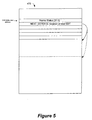
- Figure 5 shows how the data can be stored in RAM 470.
- a CAN buffer start address which may be stored in a dedicated control register indicates the start of the table entries.
- the second 32-bit data word in each table entry contains the actual address of the next table entry which may be consecutive as shown by the solid line or non-consecutive as shown by the broken line.
- a serial data stream provided by CAN protocol engine 495 comprises an identifier which is fed directly to all bit comparator units 435, 440.
- Sequencer and control unit 410 address the mask registers 415, 420 and all filter registers 425, 430 to output a corresponding bit to the bit comparator units 435, 440.
- the bit comparator units 435, 440 compare all filter register bits with the respective identifier bit within a frame. The result is further processed by comparing it to the respective mask register bit.
- each filter register 425, 430 can indicate which mask register should be used for this comparison. This function will be explained in more detail below.
- the final comparison result will be accumulated for all bits of each identifier within a frame. If a single comparison fails the acceptance signal will not be generated. If every bit comparison is positive the acceptance signal will be fed to the descriptor table control unit 460 and to a respective input of OR gate 450.
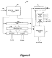
- FIG. 6 shows the CAN protocol engine 480 from Figure 1 in more detail.
- the protocol engine 480 combines several functional blocks.
- the heart of the engine 480 is the protocol finite state machine 310 (FSM).
- FSM protocol finite state machine
- This state machine sequences through the messages on a bit by bit basis, changing states of the machine as various fields of various frame types are transmitted or received.
- the FSM 310 is a sequencer controlling the sequential data stream between the RX/TX shift register 320, 325, the CRC Register 330, and the receive bus line 350 and transmit bus line 360, respectively.
- the shift registers 320, 325 can be part of the message assembly register 490. Additional components 355 and 365 are provided to convert the data streams and adapt to the respective timing on the bus lines 350 and 360.
- the FSM also controls the Error Management Logic 340 (EML) and the parallel data stream RecData between the TX/RX shift register 320, 325 and other components of the CAN module.
- EML Error Management Logic
- RecData RecData between the TX/RX shift register 320, 325 and other components of the CAN module.
- the processes of reception arbitration, transmission, and error signaling are performed according to the CAN protocol.
- the FSM 310 also handles any automatic transmission of messages on the bus line.
- the data interface to the protocol engine 480 consists of byte wide transmit and receive data. Rather than assembling and shifting an entire frame, the frames are broken into bytes.
- a receive or transmit address from the protocol FSM 310 signifies which byte of the frame is current.
- the appropriate byte from the transmit buffer is selected and presented to the engine, which then uses an 8-bit shift register to serialize the data.
- an 8-bit shift register assembles a byte which is then loaded within the appropriate byte in the message assembly buffer 490.
- the cyclic redundancy check register 330 generates the Cyclic Redundancy Check (CRC) code to be transmitted over the data bytes and checks the CRC code of incoming messages.
- the Error Management Logic (EML) 340 is responsible for the fault confinement of the CAN device. Its counters, the Receive Error Counter and the Transmit Error Counter, are incremented and decremented by commands from the Bit stream processor. According to the values of the error counters, the CAN controller is set into states error active, error passive or bus off.
- the Bit Timing Logic (BTL) within unit 355 monitors the bus line input and handles the bus line related bit timing according to the CAN protocol.
- the BTL synchronizes on a recessive to dominant bus line transition at Start of Frame and on any further recessive to dominant bus line transition, if the CAN controller itself does not transmit a dominant bit.
- the BTL also provides programmable time segments to compensate for the propagation delay time and for phase shifts and in defining the position of the Sample Point in the bit time.
- the programming of the BTL depends on the baud rate and on external physical delay times.
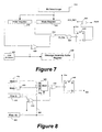
- FIG. 7 an exemplary embodiment of a comparator unit shown. The details are shown for a single Bit comparator unit but apply for all other bit comparator units accordingly.
- Numeral 600 indicates a unit providing a CAN serial data stream which is fed to a message assembly buffer register 490 and the first input of an Exclusive NOR gate 690.
- the single bit output of a filter register 620 is coupled with the second input of Exclusive NOR gate 690 whose output is connected with the first input of a NOR gate 650.
- the second input of NOR gate 650 receives the single bit output signal from mask register 630.
- the output of NOR gate 650 is coupled with the first input of an AND gate 660 whose output is coupled with the control input of a D-Flip-Flop 670.
- Input D of D-Flip-Flop 670 is coupled with a logical "low" signal such as Vcc.
- the inverting output of D-Flip-Flop 670 is coupled with the first input of AND gate 640 whose output provides the acceptance signal.
- AND gates 640 and 660 comprises second inputs ACC_RDY and BIT_RDY, respectively which are used for synchronization with the respective input signals.
- a Bit Select Logic 610 is coupled with filter register 620 and mask register 630 to select the respective bits which will be used for comparison within each frame.
- bit select logic 610 selects the respective bit in filter register 620 and mask register 630 that corresponds to the incoming bit of the serial bit stream.
- the actual comparator is formed by Exclusive NOR gate 690 which only generates a logic "high” at its output if both input signals are identical.
- NOR gate 650 is used as a mask unit to mask out a result if a respective bit within the mask register 630 is set.
- D-Flip-Flop 670 is used as a register to accumulate the results within a chain of comparisons and is preset to "1" at the start of a frame.
- Figure 8 shows another exemplary embodiment of a bit comparator unit 435, 440 with even more functionality in more detail. Again, the details are shown for Bit comparator unit 0 but may apply for all other bit comparator units accordingly.
- the outputs of mask register 415 and 420 are coupled with first and second inputs of a 4:1 multiplexer 520. Additional input 560 and 570 can be provided at the third and fourth input of multiplexer 520.
- input 560 is coupled with the output of filter register 15 which is designated by numeral 580.
- Filter register 425 comprises, for example, two additional outputs which are coupled with the select input of multiplexer 520.
- Multiplexer 520 can have any size, for example, can be expanded to a N: multiplexer increasing the number of masks to N.
- the output of multiplexer 520 is connected to the first input of a NOR gate 530.
- NOR gate 530 operates as a validation unit indicating whether a comparison result will be used or ignored.
- the second input of NOR gate 530 is coupled with the output of an Exclusive NOR gate 510 whose first input receives the bit output signal from filter register 425 and whose second input receives the serial data stream from CAN protocol engine 495.
- the output of NOR gate 530 is coupled with the control input of a D-Flip-Flop 540.
- the D-input of D-Flip-Flop 540 receives a logical low signal.
- the acceptance signal is carried at the negating output 550 of D-Flip-Flop 540.
- the first comparison stage is formed by Exclusive NOR gate 510.
- Exclusive NOR gate 510 In this stage the identifier bits of the serial bit stream are compared with the respective bits of filter register 425.
- Exclusive NOR gate 510 only generates a logic "high" at its output if both input signals are identical.
- Sequencer unit 410 selects the respective bits within filter register 425.
- Filter register 425 comprises additional data bits which indicate which mask register should be used. In this exemplary embodiment four different values can be selected. Either one of the mask registers 415 or 420 can be selected or a third value can be provided by another filter register, for example filter register 15.
- the fourth possible selection 570 can be used to indicate that no mask will be used by providing a respective level, for example, a logical "1".
- each filter register 425, 430 can be assigned an individual mask function.
- the selected mask value will be put at the first input of NOR gate 530. If the mask value indicates that the respective bit in filter register 425 should be used NOR gate 530 will operate as a controllable switch and feed the comparison result of Exclusive NOR gate 510 to the control input D-Flip-Flop 540.
- D-Flip-Flop 540 is used as a register which is preset to "1". If the result of one comparison is negative indicating no match and the respective mask bit is valid D-Flip-Flop 540 will be cleared and no acceptance signal 550 will be generated. D-Flip-Flop 540 thus will be reset to "0". D-Flip-Flop 540 will be preset to "1" again beginning with the next frame to compare another identifier as described above.
- any other type of appropriate logic can be used to implement the comparator.
- controllable switches, equivalent Boolean operators, etc. can be used.
- the validation unit can be either put in front of the comparator or after the comparator.
- the essential function of a validation unit is to either incorporate selected bits or exclude them from comparison.
Landscapes
- Engineering & Computer Science (AREA)
- Computer Networks & Wireless Communication (AREA)
- Signal Processing (AREA)
- Small-Scale Networks (AREA)
- Information Transfer Systems (AREA)
- Communication Control (AREA)
Claims (13)
- Mikrocontroller, der aufweist:einen Schreib-Lese-Speicher (470);einen Controller Area Network (CAN) Controller, der eine Steuereinheit (460) aufweist, die eine zusammengesetzte CAN Nachricht empfängt, wobei die Steuereinheit (460) eingerichtet ist unter Verwendung der zusammengesetzten CAN Nachricht einen Zwischenspeicherdeskriptortabelleneintrag zu erzeugen und diesen Zwischenspeicherdeskriptortabelleneintrag in dem Schreib-Lese-Speicher (480) zu speichern, dadurch gekennzeichnet, dass der Zwischenspeicherdeskriptortabelleneintrag zumindest einen Nachrichtenidentifikator (230) und Nutzdaten (250, 260) der CAN Nachricht und Information über einen nachfolgenden Zwischenspeicherdeskriptortabelleneintrag (220) umfasst.
- Verfahren zum Speichern einer Controller Area Network (CAN) Nachricht in einem Mikrocontroller, das die Schritte aufweist:- Empfangen einer CAN Nachricht;- Speichern der CAN Nachricht;- Erzeugen eines Zwischenspeicherdeskriptortabelleneintrags unter Verwendung der gespeicherten CAN Nachricht; und- Speichern des Zwischenspeicherdeskriptortabelleneintrag in einem Schreib-Lese-Speicher (470) des Mikrocontrollers, dadurch gekennzeichnet, dass der Zwischenspeicherdeskriptortabelleneintrag zumindest einen Nachrichtenidentifikator (230) und Nutzdaten (250, 260) der CAN Nachricht und Information über einen nachfolgenden Zwischenspeicherdeskriptortabelleneintrag (220) umfasst.
- Mikrocontroller oder Verfahren gemäß Anspruch 1 oder 2, wobei ein Zwischenspeicherdeskriptortabelleneintrag eine konstante Größe aufweist.
- Mikrocontroller oder Verfahren gemäß einem der vorherigen Ansprüche, wobei der Zwischenspeicherdeskriptortabelleneintrag weiterhin einen Framestatus (210) und einen erweiterten CAN Nachrichtenidentifikator (240) aufweist.
- Mikrocontroller oder Verfahren gemäß einem der vorherigen Ansprüche, wobei der Mikrocontroller ein 32-Bit Mikrocontroller ist und der Zwischenspeicherdeskriptortabelleneintrag aus sechs 32-Bit Worten (210 ... 260) besteht.
- Mikrocontroller oder Verfahren gemäß einem der vorherigen Ansprüche, wobei der Zwischenspeicherdeskriptortabelleneintrag ein Framestatuswort (210), ein Ort-der-nächsten-Adresse-Wort (220), ein Nachrichtenidentifikatorwort (230), ein erweitertes Nachrichtenidentifikatorwort (240), ein erstes vier Byte umfassendes Datenwort (250) und ein zweites vier Byte umfassendes Datenwort (260) aufweist.
- Mikrocontroller oder Verfahren gemäß einem der vorherigen Ansprüche, wobei der Schreib-Lese-Speicher (470) ein Dual- oder Multi-Port-Speicher ist.
- Mikrocontroller gemäß Anspruch 1, wobei der CAN Controller ein mit der Steuereinheit (460) gekoppeltes Nachrichtenaufbauzwischenspeicherschiebregister (490) aufweist.
- Mikrocontroller gemäß Anspruch 8, wobei der CAN Controller Logik (435, 440, 450) aufweist, die eine Vielzahl von Maskierungsregistern (415, 420) und eine Vielzahl von Filterregistern (425, 430) mit der Steuereinheit (460) koppelt, wobei die Logik (435, 440, 450) ein Signal erzeugt das einen gültigen Eintrag in dem Nachrichtenaufbauzwischenspeicherschiebregister (490) anzeigt.
- Verfahren gemäß Anspruch 2, wobei die CAN Nachricht sowohl eine Standard CAN Nachricht als auch eine erweiterte CAN Nachricht sein kann.
- Verfahren gemäß einem der vorherigen Verfahrensansprüche 2 bis 7, wobei der Schritt des Speicherns einer CAN Nachricht durch ein Nachrichtenaufbauzwischenspeicherschiebregister (490) ausgeführt wird.
- Verfahren gemäß Anspruch 11, wobei ein CAN Bitstrom sequentiell in das Nachrichtenaufbauzwischenspeicherschiebregister (490) verschoben wird.
- Verfahren gemäß Anspruch 11 oder 12, das weiterhin den Schritt des Erzeugens eines Gültigkeitssignals mittels einer Vielzahl von Maskierungsregistern und einer Vielzahl von Filterregistern aufweist, das einen gültigen Eintrag in dem Nachrichtenaufbauzwischenspeicherschiebregister (490) anzeigt.
Applications Claiming Priority (3)
| Application Number | Priority Date | Filing Date | Title |
|---|---|---|---|
| US18172009P | 2009-05-28 | 2009-05-28 | |
| US12/776,046 US8650356B2 (en) | 2009-05-28 | 2010-05-07 | Microcontroller with CAN module |
| PCT/US2010/035767 WO2010138416A1 (en) | 2009-05-28 | 2010-05-21 | Microcontroller with can module using a buffer description table |
Publications (2)
| Publication Number | Publication Date |
|---|---|
| EP2436150A1 EP2436150A1 (de) | 2012-04-04 |
| EP2436150B1 true EP2436150B1 (de) | 2013-04-03 |
Family
ID=43221568
Family Applications (1)
| Application Number | Title | Priority Date | Filing Date |
|---|---|---|---|
| EP10725931A Active EP2436150B1 (de) | 2009-05-28 | 2010-05-21 | Mikrokontroller mit can-modul, der eine pufferbeschreibungstabelle benutzt |
Country Status (5)
| Country | Link |
|---|---|
| US (1) | US8650356B2 (de) |
| EP (1) | EP2436150B1 (de) |
| KR (1) | KR101708876B1 (de) |
| CN (1) | CN102326363B (de) |
| WO (1) | WO2010138416A1 (de) |
Families Citing this family (22)
| Publication number | Priority date | Publication date | Assignee | Title |
|---|---|---|---|---|
| EP2668747B1 (de) * | 2011-01-25 | 2018-09-12 | ABB Schweiz AG | Übertragungsprotokoll |
| EP2521319B1 (de) * | 2011-05-02 | 2015-10-14 | Robert Bosch GmbH | CAN mit flexibler Datenrate |
| GB201206409D0 (en) * | 2012-03-26 | 2012-05-23 | Continental Automotive Systems | Method and apparatus to reduct flash memory device programming time over a C.A.N. bus |
| CN103248520A (zh) * | 2013-04-28 | 2013-08-14 | 安徽江淮汽车股份有限公司 | 一种can总线的总线脱离故障处理方法及系统 |
| EP2822230B1 (de) * | 2013-07-04 | 2017-10-18 | Omicron electronics GmbH | Datenübertragung über einen Speicher einer Kommunikationsvorrichtung |
| US9288048B2 (en) * | 2013-09-24 | 2016-03-15 | The Regents Of The University Of Michigan | Real-time frame authentication using ID anonymization in automotive networks |
| US9892073B1 (en) | 2014-10-06 | 2018-02-13 | Master Lock Company Llc | Bus addressing systems and methods using repurposed bits |
| DE102015105110A1 (de) | 2015-04-02 | 2016-10-06 | Dr. Ing. H.C. F. Porsche Aktiengesellschaft | Steuergerät zum Verbinden eines CAN-Busses mit einem Funknetzwerk und Kraftfahrzeug mit einem solchen Steuergerät |
| DE102015105134A1 (de) | 2015-04-02 | 2016-10-06 | Dr. Ing. H.C. F. Porsche Aktiengesellschaft | Steuergerät zum Verbinden eines CAN-Busses mit einem Funknetzwerk und Kraftfahrzeug mit einem solchen Steuergerät |
| DE102015105112A1 (de) | 2015-04-02 | 2016-10-06 | Dr. Ing. H.C. F. Porsche Aktiengesellschaft | Steuergerät zum Verbinden eines CAN-Busses mit einem Funknetzwerk und Kraftfahrzeug mit einem solchen Steuergerät |
| US10361934B2 (en) * | 2015-09-28 | 2019-07-23 | Nxp B.V. | Controller area network (CAN) device and method for controlling CAN traffic |
| US10212081B2 (en) | 2015-12-01 | 2019-02-19 | Marvell World Trade Ltd. | Systems and methods for implementing a time-stamped controller area network (CAN) bus message |
| DE102017002806B4 (de) * | 2017-03-23 | 2018-10-04 | WAGO Verwaltungsgesellschaft mit beschränkter Haftung | Koppler für ein Automatisierungssystem |
| CN108199941B (zh) * | 2017-12-29 | 2022-03-08 | 北京纳米维景科技有限公司 | 一种基于can2.0b的can总线通信方法 |
| TWI678902B (zh) * | 2018-11-28 | 2019-12-01 | 中華電信股份有限公司 | 針對應用進行封包處理/交換的網路系統與方法 |
| US11121910B2 (en) | 2018-12-13 | 2021-09-14 | Honeywell International Inc. | Efficient ingress-congruency determination in a network |
| CN110808891B (zh) * | 2019-09-30 | 2021-10-12 | 深圳市道通合创新能源有限公司 | 一种can过滤器合并的方法、装置及can控制器 |
| KR102275145B1 (ko) * | 2019-12-30 | 2021-07-07 | 현대오트론 주식회사 | 베이직 캔 메시지 송신 방법 및 베이직 캔 컨트롤러 |
| KR20220001350A (ko) * | 2020-06-29 | 2022-01-05 | 주식회사 엘지에너지솔루션 | 네트워크 라우팅 장치 및 방법 |
| WO2022080520A1 (ko) * | 2020-10-14 | 2022-04-21 | 엘지전자 주식회사 | 차량이 메시지를 고속으로 전송하는 방법 |
| KR102471960B1 (ko) * | 2020-11-18 | 2022-11-30 | 한국자동차연구원 | 차량용 can 통신 보안 장치 및 방법 |
| CN113852533B (zh) * | 2021-09-27 | 2022-06-07 | 北京微纳星空科技有限公司 | 一种多通道数据通信系统、方法及电子设备 |
Family Cites Families (6)
| Publication number | Priority date | Publication date | Assignee | Title |
|---|---|---|---|---|
| JP2684362B2 (ja) | 1986-06-18 | 1997-12-03 | 株式会社日立製作所 | 可変長データの記憶方式 |
| US6604156B1 (en) | 1999-09-15 | 2003-08-05 | Koninklijke Philips Electronics N.V. | Message buffer full handling in a CAN device that employs reconfigurable message buffers |
| US6944739B2 (en) * | 2001-09-20 | 2005-09-13 | Microchip Technology Incorporated | Register bank |
| CN100375484C (zh) | 2003-12-31 | 2008-03-12 | 中兴通讯股份有限公司 | Pos-phy总线与pci总线间的数据包转发的装置 |
| US7882505B2 (en) | 2005-03-25 | 2011-02-01 | Oracle America, Inc. | Method and apparatus for switching between per-thread and per-processor resource pools in multi-threaded programs |
| US7975120B2 (en) * | 2006-12-27 | 2011-07-05 | Freescale Semiconductor, Inc. | Dynamic allocation of message buffers |
-
2010
- 2010-05-07 US US12/776,046 patent/US8650356B2/en active Active
- 2010-05-21 KR KR1020117022046A patent/KR101708876B1/ko active Active
- 2010-05-21 CN CN201080008842.1A patent/CN102326363B/zh active Active
- 2010-05-21 EP EP10725931A patent/EP2436150B1/de active Active
- 2010-05-21 WO PCT/US2010/035767 patent/WO2010138416A1/en not_active Ceased
Also Published As
| Publication number | Publication date |
|---|---|
| US20100306457A1 (en) | 2010-12-02 |
| US8650356B2 (en) | 2014-02-11 |
| CN102326363A (zh) | 2012-01-18 |
| KR20120014554A (ko) | 2012-02-17 |
| KR101708876B1 (ko) | 2017-02-21 |
| EP2436150A1 (de) | 2012-04-04 |
| WO2010138416A1 (en) | 2010-12-02 |
| CN102326363B (zh) | 2014-10-29 |
Similar Documents
| Publication | Publication Date | Title |
|---|---|---|
| US8650356B2 (en) | Microcontroller with CAN module | |
| US8650341B2 (en) | Method for CAN concatenating CAN data payloads | |
| US7979594B2 (en) | Serial communications device with dynamic allocation of acceptance masks using serial implementation | |
| US6944739B2 (en) | Register bank | |
| EP0668000A1 (de) | SERIELLE SCHNITTSTELLE FüR FAHRZEUGE MIT VERRINGERTER ANZAHL VON SENDE-und EMPFANGS-PUFFERREGISTERN | |
| US20140269754A1 (en) | Computer system and method for communicating data between computers | |
| WO1994007199A1 (en) | Dma data path aligner and network adaptor utilizing same | |
| EP1430653B1 (de) | Gerät für serielles kommunikationssystem mit zuordnung von dynamischen filtern | |
| KR19980703473A (ko) | 윈도우 콤퍼레이터 | |
| US6912594B2 (en) | Serial communication device with multi-mode operation of message receive buffers | |
| US5557266A (en) | System for cascading data switches in a communication node | |
| KR20010043460A (ko) | 디지털 통신 프로세서 | |
| US7076517B2 (en) | Serial communication device with dynamic filter allocation | |
| JP2003509968A (ja) | メッセージid情報を一致idレジスタ内に書き戻すための方法およびこの方法を実行するcanマイクロコントローラ | |
| US7568074B1 (en) | Time based data storage for shared network memory switch | |
| US11487682B1 (en) | Priority queue sorting system and method with deterministic and bounded latency | |
| EP1085719A2 (de) | Benutzung der Puffergrösse-Maske in Verbindung mit Adressezeiger zum Erkennen von Puffervoll- und Pufferrücksatzbedingungen in einem CAN Mikrokontroller, der einen rekonfigurierbaren Nachrichtenpuffer benutzt | |
| US7747904B1 (en) | Error management system and method for a packet switch | |
| WO2022259832A1 (ja) | 通信装置及びデータ通信方法 |
Legal Events
| Date | Code | Title | Description |
|---|---|---|---|
| PUAI | Public reference made under article 153(3) epc to a published international application that has entered the european phase |
Free format text: ORIGINAL CODE: 0009012 |
|
| 17P | Request for examination filed |
Effective date: 20111205 |
|
| AK | Designated contracting states |
Kind code of ref document: A1 Designated state(s): AL AT BE BG CH CY CZ DE DK EE ES FI FR GB GR HR HU IE IS IT LI LT LU LV MC MK MT NL NO PL PT RO SE SI SK SM TR |
|
| DAX | Request for extension of the european patent (deleted) | ||
| RIC1 | Information provided on ipc code assigned before grant |
Ipc: H04L 12/56 20060101ALI20120828BHEP Ipc: H04L 12/413 20060101AFI20120828BHEP Ipc: B60R 16/023 20060101ALI20120828BHEP |
|
| GRAP | Despatch of communication of intention to grant a patent |
Free format text: ORIGINAL CODE: EPIDOSNIGR1 |
|
| GRAS | Grant fee paid |
Free format text: ORIGINAL CODE: EPIDOSNIGR3 |
|
| GRAA | (expected) grant |
Free format text: ORIGINAL CODE: 0009210 |
|
| RIC1 | Information provided on ipc code assigned before grant |
Ipc: H04L 12/413 20060101AFI20130220BHEP Ipc: B60R 16/023 20060101ALI20130220BHEP Ipc: H04L 12/70 20130101ALI20130220BHEP |
|
| AK | Designated contracting states |
Kind code of ref document: B1 Designated state(s): AL AT BE BG CH CY CZ DE DK EE ES FI FR GB GR HR HU IE IS IT LI LT LU LV MC MK MT NL NO PL PT RO SE SI SK SM TR |
|
| REG | Reference to a national code |
Ref country code: GB Ref legal event code: FG4D |
|
| REG | Reference to a national code |
Ref country code: CH Ref legal event code: EP Ref country code: AT Ref legal event code: REF Ref document number: 605317 Country of ref document: AT Kind code of ref document: T Effective date: 20130415 |
|
| REG | Reference to a national code |
Ref country code: IE Ref legal event code: FG4D |
|
| REG | Reference to a national code |
Ref country code: DE Ref legal event code: R096 Ref document number: 602010006084 Country of ref document: DE Effective date: 20130529 |
|
| REG | Reference to a national code |
Ref country code: AT Ref legal event code: MK05 Ref document number: 605317 Country of ref document: AT Kind code of ref document: T Effective date: 20130403 |
|
| PG25 | Lapsed in a contracting state [announced via postgrant information from national office to epo] |
Ref country code: SI Free format text: LAPSE BECAUSE OF FAILURE TO SUBMIT A TRANSLATION OF THE DESCRIPTION OR TO PAY THE FEE WITHIN THE PRESCRIBED TIME-LIMIT Effective date: 20130403 |
|
| REG | Reference to a national code |
Ref country code: NL Ref legal event code: T3 |
|
| REG | Reference to a national code |
Ref country code: LT Ref legal event code: MG4D |
|
| PG25 | Lapsed in a contracting state [announced via postgrant information from national office to epo] |
Ref country code: GR Free format text: LAPSE BECAUSE OF FAILURE TO SUBMIT A TRANSLATION OF THE DESCRIPTION OR TO PAY THE FEE WITHIN THE PRESCRIBED TIME-LIMIT Effective date: 20130704 Ref country code: PT Free format text: LAPSE BECAUSE OF FAILURE TO SUBMIT A TRANSLATION OF THE DESCRIPTION OR TO PAY THE FEE WITHIN THE PRESCRIBED TIME-LIMIT Effective date: 20130805 Ref country code: NO Free format text: LAPSE BECAUSE OF FAILURE TO SUBMIT A TRANSLATION OF THE DESCRIPTION OR TO PAY THE FEE WITHIN THE PRESCRIBED TIME-LIMIT Effective date: 20130703 Ref country code: SE Free format text: LAPSE BECAUSE OF FAILURE TO SUBMIT A TRANSLATION OF THE DESCRIPTION OR TO PAY THE FEE WITHIN THE PRESCRIBED TIME-LIMIT Effective date: 20130403 Ref country code: AT Free format text: LAPSE BECAUSE OF FAILURE TO SUBMIT A TRANSLATION OF THE DESCRIPTION OR TO PAY THE FEE WITHIN THE PRESCRIBED TIME-LIMIT Effective date: 20130403 Ref country code: ES Free format text: LAPSE BECAUSE OF FAILURE TO SUBMIT A TRANSLATION OF THE DESCRIPTION OR TO PAY THE FEE WITHIN THE PRESCRIBED TIME-LIMIT Effective date: 20130714 Ref country code: BE Free format text: LAPSE BECAUSE OF FAILURE TO SUBMIT A TRANSLATION OF THE DESCRIPTION OR TO PAY THE FEE WITHIN THE PRESCRIBED TIME-LIMIT Effective date: 20130403 Ref country code: IS Free format text: LAPSE BECAUSE OF FAILURE TO SUBMIT A TRANSLATION OF THE DESCRIPTION OR TO PAY THE FEE WITHIN THE PRESCRIBED TIME-LIMIT Effective date: 20130803 Ref country code: LT Free format text: LAPSE BECAUSE OF FAILURE TO SUBMIT A TRANSLATION OF THE DESCRIPTION OR TO PAY THE FEE WITHIN THE PRESCRIBED TIME-LIMIT Effective date: 20130403 Ref country code: FI Free format text: LAPSE BECAUSE OF FAILURE TO SUBMIT A TRANSLATION OF THE DESCRIPTION OR TO PAY THE FEE WITHIN THE PRESCRIBED TIME-LIMIT Effective date: 20130403 |
|
| PG25 | Lapsed in a contracting state [announced via postgrant information from national office to epo] |
Ref country code: PL Free format text: LAPSE BECAUSE OF FAILURE TO SUBMIT A TRANSLATION OF THE DESCRIPTION OR TO PAY THE FEE WITHIN THE PRESCRIBED TIME-LIMIT Effective date: 20130403 Ref country code: BG Free format text: LAPSE BECAUSE OF FAILURE TO SUBMIT A TRANSLATION OF THE DESCRIPTION OR TO PAY THE FEE WITHIN THE PRESCRIBED TIME-LIMIT Effective date: 20130703 Ref country code: LV Free format text: LAPSE BECAUSE OF FAILURE TO SUBMIT A TRANSLATION OF THE DESCRIPTION OR TO PAY THE FEE WITHIN THE PRESCRIBED TIME-LIMIT Effective date: 20130403 Ref country code: CY Free format text: LAPSE BECAUSE OF FAILURE TO SUBMIT A TRANSLATION OF THE DESCRIPTION OR TO PAY THE FEE WITHIN THE PRESCRIBED TIME-LIMIT Effective date: 20130403 Ref country code: HR Free format text: LAPSE BECAUSE OF FAILURE TO SUBMIT A TRANSLATION OF THE DESCRIPTION OR TO PAY THE FEE WITHIN THE PRESCRIBED TIME-LIMIT Effective date: 20130403 |
|
| PG25 | Lapsed in a contracting state [announced via postgrant information from national office to epo] |
Ref country code: MC Free format text: LAPSE BECAUSE OF FAILURE TO SUBMIT A TRANSLATION OF THE DESCRIPTION OR TO PAY THE FEE WITHIN THE PRESCRIBED TIME-LIMIT Effective date: 20130403 Ref country code: EE Free format text: LAPSE BECAUSE OF FAILURE TO SUBMIT A TRANSLATION OF THE DESCRIPTION OR TO PAY THE FEE WITHIN THE PRESCRIBED TIME-LIMIT Effective date: 20130403 Ref country code: SK Free format text: LAPSE BECAUSE OF FAILURE TO SUBMIT A TRANSLATION OF THE DESCRIPTION OR TO PAY THE FEE WITHIN THE PRESCRIBED TIME-LIMIT Effective date: 20130403 Ref country code: CZ Free format text: LAPSE BECAUSE OF FAILURE TO SUBMIT A TRANSLATION OF THE DESCRIPTION OR TO PAY THE FEE WITHIN THE PRESCRIBED TIME-LIMIT Effective date: 20130403 Ref country code: DK Free format text: LAPSE BECAUSE OF FAILURE TO SUBMIT A TRANSLATION OF THE DESCRIPTION OR TO PAY THE FEE WITHIN THE PRESCRIBED TIME-LIMIT Effective date: 20130403 |
|
| PLBE | No opposition filed within time limit |
Free format text: ORIGINAL CODE: 0009261 |
|
| STAA | Information on the status of an ep patent application or granted ep patent |
Free format text: STATUS: NO OPPOSITION FILED WITHIN TIME LIMIT |
|
| REG | Reference to a national code |
Ref country code: IE Ref legal event code: MM4A |
|
| PG25 | Lapsed in a contracting state [announced via postgrant information from national office to epo] |
Ref country code: RO Free format text: LAPSE BECAUSE OF FAILURE TO SUBMIT A TRANSLATION OF THE DESCRIPTION OR TO PAY THE FEE WITHIN THE PRESCRIBED TIME-LIMIT Effective date: 20130403 Ref country code: IT Free format text: LAPSE BECAUSE OF FAILURE TO SUBMIT A TRANSLATION OF THE DESCRIPTION OR TO PAY THE FEE WITHIN THE PRESCRIBED TIME-LIMIT Effective date: 20130403 |
|
| 26N | No opposition filed |
Effective date: 20140106 |
|
| REG | Reference to a national code |
Ref country code: DE Ref legal event code: R097 Ref document number: 602010006084 Country of ref document: DE Effective date: 20140106 |
|
| PG25 | Lapsed in a contracting state [announced via postgrant information from national office to epo] |
Ref country code: IE Free format text: LAPSE BECAUSE OF NON-PAYMENT OF DUE FEES Effective date: 20130521 |
|
| REG | Reference to a national code |
Ref country code: CH Ref legal event code: PL |
|
| GBPC | Gb: european patent ceased through non-payment of renewal fee |
Effective date: 20140521 |
|
| PG25 | Lapsed in a contracting state [announced via postgrant information from national office to epo] |
Ref country code: CH Free format text: LAPSE BECAUSE OF NON-PAYMENT OF DUE FEES Effective date: 20140531 Ref country code: LI Free format text: LAPSE BECAUSE OF NON-PAYMENT OF DUE FEES Effective date: 20140531 |
|
| PG25 | Lapsed in a contracting state [announced via postgrant information from national office to epo] |
Ref country code: MT Free format text: LAPSE BECAUSE OF FAILURE TO SUBMIT A TRANSLATION OF THE DESCRIPTION OR TO PAY THE FEE WITHIN THE PRESCRIBED TIME-LIMIT Effective date: 20130403 |
|
| PG25 | Lapsed in a contracting state [announced via postgrant information from national office to epo] |
Ref country code: GB Free format text: LAPSE BECAUSE OF NON-PAYMENT OF DUE FEES Effective date: 20140521 Ref country code: SM Free format text: LAPSE BECAUSE OF FAILURE TO SUBMIT A TRANSLATION OF THE DESCRIPTION OR TO PAY THE FEE WITHIN THE PRESCRIBED TIME-LIMIT Effective date: 20130403 |
|
| PG25 | Lapsed in a contracting state [announced via postgrant information from national office to epo] |
Ref country code: TR Free format text: LAPSE BECAUSE OF FAILURE TO SUBMIT A TRANSLATION OF THE DESCRIPTION OR TO PAY THE FEE WITHIN THE PRESCRIBED TIME-LIMIT Effective date: 20130403 |
|
| PG25 | Lapsed in a contracting state [announced via postgrant information from national office to epo] |
Ref country code: HU Free format text: LAPSE BECAUSE OF FAILURE TO SUBMIT A TRANSLATION OF THE DESCRIPTION OR TO PAY THE FEE WITHIN THE PRESCRIBED TIME-LIMIT; INVALID AB INITIO Effective date: 20100521 Ref country code: LU Free format text: LAPSE BECAUSE OF NON-PAYMENT OF DUE FEES Effective date: 20130521 Ref country code: MK Free format text: LAPSE BECAUSE OF FAILURE TO SUBMIT A TRANSLATION OF THE DESCRIPTION OR TO PAY THE FEE WITHIN THE PRESCRIBED TIME-LIMIT Effective date: 20130403 |
|
| REG | Reference to a national code |
Ref country code: FR Ref legal event code: PLFP Year of fee payment: 7 |
|
| REG | Reference to a national code |
Ref country code: FR Ref legal event code: PLFP Year of fee payment: 8 |
|
| REG | Reference to a national code |
Ref country code: FR Ref legal event code: PLFP Year of fee payment: 9 |
|
| PG25 | Lapsed in a contracting state [announced via postgrant information from national office to epo] |
Ref country code: AL Free format text: LAPSE BECAUSE OF FAILURE TO SUBMIT A TRANSLATION OF THE DESCRIPTION OR TO PAY THE FEE WITHIN THE PRESCRIBED TIME-LIMIT Effective date: 20130403 |
|
| P01 | Opt-out of the competence of the unified patent court (upc) registered |
Effective date: 20230528 |
|
| PGFP | Annual fee paid to national office [announced via postgrant information from national office to epo] |
Ref country code: NL Payment date: 20250423 Year of fee payment: 16 |
|
| PGFP | Annual fee paid to national office [announced via postgrant information from national office to epo] |
Ref country code: DE Payment date: 20250423 Year of fee payment: 16 |
|
| PGFP | Annual fee paid to national office [announced via postgrant information from national office to epo] |
Ref country code: FR Payment date: 20250424 Year of fee payment: 16 |