EP2435754B1 - Ceramic illumination device - Google Patents
Ceramic illumination device Download PDFInfo
- Publication number
- EP2435754B1 EP2435754B1 EP10727919.2A EP10727919A EP2435754B1 EP 2435754 B1 EP2435754 B1 EP 2435754B1 EP 10727919 A EP10727919 A EP 10727919A EP 2435754 B1 EP2435754 B1 EP 2435754B1
- Authority
- EP
- European Patent Office
- Prior art keywords
- illumination device
- carrier
- envelope
- light source
- light
- Prior art date
- Legal status (The legal status is an assumption and is not a legal conclusion. Google has not performed a legal analysis and makes no representation as to the accuracy of the status listed.)
- Active
Links
- 238000005286 illumination Methods 0.000 title claims description 78
- 239000000919 ceramic Substances 0.000 title description 6
- 229910010293 ceramic material Inorganic materials 0.000 claims description 19
- PNEYBMLMFCGWSK-UHFFFAOYSA-N Alumina Chemical compound [O-2].[O-2].[O-2].[Al+3].[Al+3] PNEYBMLMFCGWSK-UHFFFAOYSA-N 0.000 claims description 16
- 239000000463 material Substances 0.000 description 11
- 239000000969 carrier Substances 0.000 description 6
- 229910052593 corundum Inorganic materials 0.000 description 5
- 229910019655 synthetic inorganic crystalline material Inorganic materials 0.000 description 5
- 229910001845 yogo sapphire Inorganic materials 0.000 description 5
- 239000007787 solid Substances 0.000 description 4
- 229910019901 yttrium aluminum garnet Inorganic materials 0.000 description 4
- PMHQVHHXPFUNSP-UHFFFAOYSA-M copper(1+);methylsulfanylmethane;bromide Chemical compound Br[Cu].CSC PMHQVHHXPFUNSP-UHFFFAOYSA-M 0.000 description 3
- VYPSYNLAJGMNEJ-UHFFFAOYSA-N Silicium dioxide Chemical compound O=[Si]=O VYPSYNLAJGMNEJ-UHFFFAOYSA-N 0.000 description 2
- GWEVSGVZZGPLCZ-UHFFFAOYSA-N Titan oxide Chemical compound O=[Ti]=O GWEVSGVZZGPLCZ-UHFFFAOYSA-N 0.000 description 2
- MCMNRKCIXSYSNV-UHFFFAOYSA-N Zirconium dioxide Chemical compound O=[Zr]=O MCMNRKCIXSYSNV-UHFFFAOYSA-N 0.000 description 2
- 230000005540 biological transmission Effects 0.000 description 2
- 230000005611 electricity Effects 0.000 description 2
- 238000000034 method Methods 0.000 description 2
- 230000008569 process Effects 0.000 description 2
- 230000009471 action Effects 0.000 description 1
- 230000004075 alteration Effects 0.000 description 1
- 239000011230 binding agent Substances 0.000 description 1
- 229910052681 coesite Inorganic materials 0.000 description 1
- 238000001816 cooling Methods 0.000 description 1
- 229910052906 cristobalite Inorganic materials 0.000 description 1
- 230000001419 dependent effect Effects 0.000 description 1
- 239000002019 doping agent Substances 0.000 description 1
- 230000000694 effects Effects 0.000 description 1
- 239000002223 garnet Substances 0.000 description 1
- 239000011521 glass Substances 0.000 description 1
- 239000003292 glue Substances 0.000 description 1
- 230000017525 heat dissipation Effects 0.000 description 1
- 150000002500 ions Chemical class 0.000 description 1
- 230000005226 mechanical processes and functions Effects 0.000 description 1
- 238000012986 modification Methods 0.000 description 1
- 230000004048 modification Effects 0.000 description 1
- -1 one or more of Sc Chemical class 0.000 description 1
- 230000003287 optical effect Effects 0.000 description 1
- 239000000843 powder Substances 0.000 description 1
- 238000009877 rendering Methods 0.000 description 1
- 230000004044 response Effects 0.000 description 1
- 239000000377 silicon dioxide Substances 0.000 description 1
- 238000001228 spectrum Methods 0.000 description 1
- 239000007858 starting material Substances 0.000 description 1
- 229910052682 stishovite Inorganic materials 0.000 description 1
- 229910052905 tridymite Inorganic materials 0.000 description 1
- RUDFQVOCFDJEEF-UHFFFAOYSA-N yttrium(III) oxide Inorganic materials [O-2].[O-2].[O-2].[Y+3].[Y+3] RUDFQVOCFDJEEF-UHFFFAOYSA-N 0.000 description 1
Images


Classifications
-
- F—MECHANICAL ENGINEERING; LIGHTING; HEATING; WEAPONS; BLASTING
- F21—LIGHTING
- F21K—NON-ELECTRIC LIGHT SOURCES USING LUMINESCENCE; LIGHT SOURCES USING ELECTROCHEMILUMINESCENCE; LIGHT SOURCES USING CHARGES OF COMBUSTIBLE MATERIAL; LIGHT SOURCES USING SEMICONDUCTOR DEVICES AS LIGHT-GENERATING ELEMENTS; LIGHT SOURCES NOT OTHERWISE PROVIDED FOR
- F21K9/00—Light sources using semiconductor devices as light-generating elements, e.g. using light-emitting diodes [LED] or lasers
- F21K9/20—Light sources comprising attachment means
- F21K9/23—Retrofit light sources for lighting devices with a single fitting for each light source, e.g. for substitution of incandescent lamps with bayonet or threaded fittings
- F21K9/232—Retrofit light sources for lighting devices with a single fitting for each light source, e.g. for substitution of incandescent lamps with bayonet or threaded fittings specially adapted for generating an essentially omnidirectional light distribution, e.g. with a glass bulb
-
- F—MECHANICAL ENGINEERING; LIGHTING; HEATING; WEAPONS; BLASTING
- F21—LIGHTING
- F21V—FUNCTIONAL FEATURES OR DETAILS OF LIGHTING DEVICES OR SYSTEMS THEREOF; STRUCTURAL COMBINATIONS OF LIGHTING DEVICES WITH OTHER ARTICLES, NOT OTHERWISE PROVIDED FOR
- F21V19/00—Fastening of light sources or lamp holders
- F21V19/001—Fastening of light sources or lamp holders the light sources being semiconductors devices, e.g. LEDs
- F21V19/003—Fastening of light source holders, e.g. of circuit boards or substrates holding light sources
-
- F—MECHANICAL ENGINEERING; LIGHTING; HEATING; WEAPONS; BLASTING
- F21—LIGHTING
- F21V—FUNCTIONAL FEATURES OR DETAILS OF LIGHTING DEVICES OR SYSTEMS THEREOF; STRUCTURAL COMBINATIONS OF LIGHTING DEVICES WITH OTHER ARTICLES, NOT OTHERWISE PROVIDED FOR
- F21V29/00—Protecting lighting devices from thermal damage; Cooling or heating arrangements specially adapted for lighting devices or systems
- F21V29/50—Cooling arrangements
- F21V29/70—Cooling arrangements characterised by passive heat-dissipating elements, e.g. heat-sinks
- F21V29/71—Cooling arrangements characterised by passive heat-dissipating elements, e.g. heat-sinks using a combination of separate elements interconnected by heat-conducting means, e.g. with heat pipes or thermally conductive bars between separate heat-sink elements
-
- F—MECHANICAL ENGINEERING; LIGHTING; HEATING; WEAPONS; BLASTING
- F21—LIGHTING
- F21V—FUNCTIONAL FEATURES OR DETAILS OF LIGHTING DEVICES OR SYSTEMS THEREOF; STRUCTURAL COMBINATIONS OF LIGHTING DEVICES WITH OTHER ARTICLES, NOT OTHERWISE PROVIDED FOR
- F21V29/00—Protecting lighting devices from thermal damage; Cooling or heating arrangements specially adapted for lighting devices or systems
- F21V29/85—Protecting lighting devices from thermal damage; Cooling or heating arrangements specially adapted for lighting devices or systems characterised by the material
- F21V29/86—Ceramics or glass
-
- F—MECHANICAL ENGINEERING; LIGHTING; HEATING; WEAPONS; BLASTING
- F21—LIGHTING
- F21V—FUNCTIONAL FEATURES OR DETAILS OF LIGHTING DEVICES OR SYSTEMS THEREOF; STRUCTURAL COMBINATIONS OF LIGHTING DEVICES WITH OTHER ARTICLES, NOT OTHERWISE PROVIDED FOR
- F21V3/00—Globes; Bowls; Cover glasses
- F21V3/02—Globes; Bowls; Cover glasses characterised by the shape
-
- F—MECHANICAL ENGINEERING; LIGHTING; HEATING; WEAPONS; BLASTING
- F21—LIGHTING
- F21V—FUNCTIONAL FEATURES OR DETAILS OF LIGHTING DEVICES OR SYSTEMS THEREOF; STRUCTURAL COMBINATIONS OF LIGHTING DEVICES WITH OTHER ARTICLES, NOT OTHERWISE PROVIDED FOR
- F21V3/00—Globes; Bowls; Cover glasses
- F21V3/04—Globes; Bowls; Cover glasses characterised by materials, surface treatments or coatings
- F21V3/06—Globes; Bowls; Cover glasses characterised by materials, surface treatments or coatings characterised by the material
-
- H—ELECTRICITY
- H01—ELECTRIC ELEMENTS
- H01L—SEMICONDUCTOR DEVICES NOT COVERED BY CLASS H10
- H01L33/00—Semiconductor devices with at least one potential-jump barrier or surface barrier specially adapted for light emission; Processes or apparatus specially adapted for the manufacture or treatment thereof or of parts thereof; Details thereof
- H01L33/48—Semiconductor devices with at least one potential-jump barrier or surface barrier specially adapted for light emission; Processes or apparatus specially adapted for the manufacture or treatment thereof or of parts thereof; Details thereof characterised by the semiconductor body packages
- H01L33/64—Heat extraction or cooling elements
- H01L33/641—Heat extraction or cooling elements characterized by the materials
-
- F—MECHANICAL ENGINEERING; LIGHTING; HEATING; WEAPONS; BLASTING
- F21—LIGHTING
- F21V—FUNCTIONAL FEATURES OR DETAILS OF LIGHTING DEVICES OR SYSTEMS THEREOF; STRUCTURAL COMBINATIONS OF LIGHTING DEVICES WITH OTHER ARTICLES, NOT OTHERWISE PROVIDED FOR
- F21V3/00—Globes; Bowls; Cover glasses
- F21V3/04—Globes; Bowls; Cover glasses characterised by materials, surface treatments or coatings
-
- F—MECHANICAL ENGINEERING; LIGHTING; HEATING; WEAPONS; BLASTING
- F21—LIGHTING
- F21Y—INDEXING SCHEME ASSOCIATED WITH SUBCLASSES F21K, F21L, F21S and F21V, RELATING TO THE FORM OR THE KIND OF THE LIGHT SOURCES OR OF THE COLOUR OF THE LIGHT EMITTED
- F21Y2107/00—Light sources with three-dimensionally disposed light-generating elements
- F21Y2107/90—Light sources with three-dimensionally disposed light-generating elements on two opposite sides of supports or substrates
-
- F—MECHANICAL ENGINEERING; LIGHTING; HEATING; WEAPONS; BLASTING
- F21—LIGHTING
- F21Y—INDEXING SCHEME ASSOCIATED WITH SUBCLASSES F21K, F21L, F21S and F21V, RELATING TO THE FORM OR THE KIND OF THE LIGHT SOURCES OR OF THE COLOUR OF THE LIGHT EMITTED
- F21Y2115/00—Light-generating elements of semiconductor light sources
- F21Y2115/10—Light-emitting diodes [LED]
Definitions
- the present invention relates to an illumination device and, in particular, to an illumination device made of ceramic material.
- LED lamps Light-emitting-diode (LED) lamps are known in the art.
- a LED lamp is a lamp that uses LEDs as the source of light.
- multiple diodes may be used for either increasing the output power of the lamp or for providing a white light as a single LED emits in a narrow band of wavelengths.
- LED lamps may be used for general lighting or even more specific lighting as the colour and the output power may be tuned.
- a lamp or illumination device comprises a light source arranged to generate light and mounted on, or at least connected to, a circuit board.
- the light source is arranged within an encapsulating housing usually having the shape of a bulb.
- the design of an illumination device needs to take into account the evacuation of heat generated by the light source(s) and/or the electronics connected to the light source(s).
- a white LED-based lighting device comprising a group of solid state light emitting diodes, electronics to activate the light emitting diodes and an encapsulating housing.
- the encapsulating housing For conducting or transferring outwardly heat generated from within the white light LED device, the encapsulating housing includes air vents and heat-sinking components.
- a disadvantage of prior art systems may be that they require specific components for evacuation of heat (e.g. air-vents and an arrangement of heat sinking components), thereby rendering the design of the system rather complex or resulting in an expensive system.
- specific components for evacuation of heat e.g. air-vents and an arrangement of heat sinking components
- an illumination device as defined in claim 1 is provided.
- the illumination device comprises a light source arranged to generate light, a carrier arranged to support the light source and an envelope enclosing the light source and the carrier.
- the light source is in thermal contact with the carrier and the carrier is arranged in thermal contact with the envelope for dissipating heat out of the illumination device.
- Both the envelope and the carrier are made of ceramic material.
- the envelope (or bulb) of the illumination device may act as a heat sink and serve for dissipating heat (e.g. generated by the light source or any electronics connected to the light source) out of the illumination device.
- the light source is arranged in thermal contact with a carrier which itself is in thermal contact with the envelope and both the carrier and the envelope comprises ceramic material (a kind of material having good thermal conductivity).
- the present invention is advantageous in that it does not require any additional (or specific) components for heat transfer since this function is provided by the specific arrangement of the main parts of the illumination device, namely the light source(s), the carrier and, in particular, the envelope.
- the whole surface of the illumination device, i.e. the envelope acts as a heat sink, thereby providing a relatively large surface for heat transfer.
- the present invention is also advantageous in that an effective transfer of heat to the outside environment of the illumination device is provided.
- the envelope may comprise a transmissive region arranged to transmit at least part of the light generated by the light source (especially when the light source emits in the visible range of the wavelength spectrum, i.e. 380-780 nm).
- the transmissive region may be translucent (transmitting and scattering of light) or be transparent (substantial unhindered transmission).
- the transmissive region is translucent, thereby preventing a user from perceiving the light source(s) and optional electronics within the envelope.
- the envelope or encapsulating housing of the illumination device is advantageous in that it integrates a number of functionalities such as an optical function, a thermal function and a mechanical function.
- the carrier may comprise a transmissive region arranged to transmit at least part of the light generated by the light source.
- the carrier may comprise a reflective region arranged to reflect at least part of the light generated by the light source(s).
- the ceramic material may be poly crystalline aluminium oxide (PCA), which is advantageous in that it is a translucent ceramic material having a good thermal conductivity (in the range of about 20 W/mK).
- PCA poly crystalline aluminium oxide
- the ceramic material may have a thermal conductivity of at least about 5 W/mK.
- the envelope may comprise at least two enveloping parts which, when joined together, form the envelope or encapsulating housing of the illumination device.
- the present embodiment is advantageous in that it provides a convenient design which facilitates the assembly of the illumination device (such as a lamp or spot light).
- the illumination device such as a lamp or spot light.
- the light source and the carrier may conveniently be mounted together while the two enveloping parts are separated and then enclosed in the envelope by joining the two enveloping parts. It will be appreciated that more than two enveloping parts may be employed and that the present embodiment is not limited to an illumination device comprising an envelope made of only two enveloping parts.
- the envelope may have the shape of a bulb (or lamp bulb).
- the enveloping parts of the envelope as defined in the above embodiment may be two bulb halves.
- an enveloping part and at least part of the carrier may form a single integrated part, which is advantageous in that the number of components is reduced, thereby facilitating the assembly of the illumination device even further.
- the present embodiment is also advantageous in that the enveloping part and the part of the carrier (e.g. a bulb half and half of the carrier) may be manufactured as one single part from one single mould.
- the corresponding enveloping part(s) and part of the carrier for forming the envelope and the carrier may also be manufactured from one single mould, preferably the same mould.
- the carrier may be arranged at a junction between two enveloping parts.
- the carrier and the enveloping parts are separate parts.
- the enveloping parts may advantageously be configured to fit one to another, thereby facilitating the assembly of the illumination device.
- the carrier may be arranged along an axis extending from the base of the illumination device to its top.
- the carrier may be arranged along a direction crossing an axis extending from the base of the illumination device to its top.
- the carrier divides the space defined by the envelope in at least two compartments. A plurality of light sources may then advantageously be used and distributed on each side of the carrier such that an uniform illumination is provided.
- the light source may be at least one light emitting diode (LED) or at least one LED package.
- the light source may for instance comprise an RGB LED (red green blue light emitting diode), or a plurality of diodes arranged to provide white light, such as an RGB combination, or a combination of blue and yellow, or a combination of blue, yellow and red, etc.
- the illumination device may be arranged to provide coloured light.
- the light source may also comprise a plurality of light sources (such as a plurality of LEDs), that is (are) able to provide light at different predetermined wavelengths, depending upon the driving conditions.
- the illumination device may further comprise a controller (attached to or external from the illumination device), arranged to control the colour of the illumination device light in response to a sensor signal or a user input device signal.
- LED may also refer to a light source (or a plurality of light sources) in general, unless indicated otherwise or clear from the context, but preferably refers to a LED. Further, the term “LED” especially refers to solid state lighting (solid state LEDs).
- the light source may emit light in the visible range, but may also, in another embodiment, alternatively or additionally emit in the UV range.
- the light source may comprise a LED.
- the light source is a LED arranged to generate blue light.
- the blue light emitting source may be used per se, or may be used in combination with luminescent material, e.g. arranged at the envelope or at least one of the enveloping parts, such as to provide white light, or may be used in combination with one or more other LEDs generating light at other wavelengths. Combinations of such embodiments may also be applied.
- the term “at least” may in embodiments also indicate “all” or “completely”.
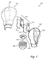
- Figure 1 shows an exploded view of an illumination device 100 according to an embodiment of the present invention.
- the illumination device comprises a light source 110 arranged to generate light.
- the light source 110 corresponds to a plurality of LED packages 111, 112, 113 and 114.
- Figure 1 shows a plurality of LED packages to form the light source 110, a single LED or LED package may also be used.
- the illumination device 100 comprises a carrier 120 (see Figure 4c ) which is represented by two carrier parts 121 and 122 (or a first carrier 121 and a second carrier 122) in Figure 1 .
- the carrier 120 is arranged to support the light source 110 or LED packages 111-114.
- the two carrier parts 121 and 122 may also be referred to as the single carrier 120, when the two parts are indeed joined together, such as in Figure 4c .
- the illumination device 100 comprises also an envelope 130 for enclosing the light source 110 and the carrier 120.
- the envelope 130 is represented by two enveloping parts 131 and 132 which, when joined together, form the envelope or encapsulating housing 130, such as shown in Figure 4c .
- the envelope may be made of two enveloping parts, the present invention is not limited to such a design and an envelope made of a single part or more than two parts may also be envisaged.
- the light sources 111-114 are arranged in thermal contact with the carrier 120 (or carrier parts 121 and 122 in Figure 1 ) and the carrier 120 is arranged in thermal contact with the envelope 130 (or enveloping parts 131 and 132, respectively, in Figure 1 ).
- the carrier 120 can be inserted in the envelope 130.
- the carrier may have any shape.
- the envelope 130 has a standard bulb shape and the carrier 120 may then preferably have the shape of a disk or part of a disk.
- the contact surface between the carrier 120 and the envelope 130 may advantageously not be punctual but, instead, extends along a portion of the inside of the envelope 130.
- the contact surface may for instance extends along a circumference (or part of a circumference) of the envelope such that an effective heat transfer is provided.
- heat may be generated by the light source(s) 111-114 and be dissipated out of the illumination device 100 via the carrier 120 and the envelope 130.
- Both the envelope and the carrier comprises ceramic material for improving the heat transfer out of the illumination device.
- Ceramic is known in the art and may especially refer to an inorganic, non-metallic solid prepared by the action of heat and subsequent cooling. Ceramic materials may have a crystalline or partly crystalline structure, or may be amorphous, i.e., a glass. Most common ceramics are crystalline. The term ceramic especially relates to materials that have sintered together and form pieces (in contrast to powders). The ceramics used herein are preferably polycrystalline ceramics.
- the ceramic material may for instance be based on one or more materials selected from the group consisting of Al 2 O 3 , AlN, SiO 2 , Y 3 Al 5 O 12 (YAG), an Y 3 Al 5 O 12 analogue, Y 2 O 3 and TiO 2 , and ZrO 2 .
- YAG Y 3 Al 5 O 12
- the term an Y 3 Al 5 O 12 analogue refers to garnet systems having substantially the same lattice structure as YAG, but wherein Y and/or Al and/or O, especially Y and/or Al are at least partly replaced by another ion, such as one or more of Sc, La, Lu and G, respectively.
- the ceramic material may be Al 2 O 3 , which is a translucent material.
- Al 2 O 3 can also be made highly reflective when it is sintered at a temperature in the range of about 1300-1700°C, such as in the range of about 1300-1500°C, like 1300-1450°C. This material is also known in the art as "brown" PCA (polycrystalline alumina).
- the term "based on” indicates that the starting materials to make the ceramic material substantially consist of one or more of the herein indicated materials, such as for instance Al 2 O 3 or Y 3 Al 5 O 12 (YAG). This does however not exclude the presence of small amounts of (remaining) binder material, or dopants, such as Ti for Al 2 O 3 , or in an embodiment Ce for YAG.
- the ceramic material may have a relatively good thermal conductivity.
- the thermal conductivity is at least about 5 W/mK, such as at least about 15 W/mK, even more preferably at least about 100 W/mK.
- YAG has a thermal conductivity in the range of about 6 W/mK, poly crystalline alumina (PCA) in the range of about 20 W/mK, and AlN (aluminum nitride) in the range of about 150 W/mK or larger.
- the envelope 130 may especially be arranged to receive all light from the light source(s) 111-114. Further, the envelope 130 may especially be arranged to allow escape of light of the light source(s) 111-114.
- the envelope 130 may thus also be indicated as a mixing chamber. Mixing may also be of relevance when a luminescent material is used that is arranged remote from a light source (from which it absorbs part of the light to provide luminescent material light), e.g. arranged at the envelope or part of the envelope.
- the envelope 130 may comprise a transmissive region arranged to transmit at least part of the light generated by the light sources 111-114.
- the envelope 130 may be made of a material having light transmissive properties such that an efficient transmission of light through the envelope is achieved.
- the carrier 120 may also comprise a transmissive region, which is advantageous in that light coming from a compartment of the envelope in direction to the carrier may be transmitted through the carrier and, then, transmitted out of the illumination device via the envelope 130.
- the carrier 120 may comprise a reflective region arranged to reflect at least part of the light generated by the light source(s), which is advantageous in that light emitted in a compartment of the envelope and directed towards the carrier may be reflected against the carrier and transmitted out of the illumination device via the same compartment of the envelope.
- the carrier may be designed with a number of regions being either transmissive or reflective such that, e.g., a desired light distribution is achieved.
- the ceramic material may be poly crystalline aluminium oxide (PCA), which is advantageous in that it is a translucent ceramic material having a good thermal conductivity (of about 20 W/mK).
- PCA poly crystalline aluminium oxide
- the ceramic material may have a thermal conductivity of at least about 150 W/mK such that an effective heat transfer is provided.
- the envelope 130 may be bulb-shaped and the enveloping parts 131 and 132 may be two bulb halves, thereby providing an illumination device which has a standard lamp shape.
- the light source(s) 111-114 of the illumination device may advantageously be distributed on each side of the carrier 120 (or first and second carriers 121 and 122 in Figure 1 ) for improving the uniformity of the light emitted from the illumination device 100.
- the illumination device 100 may also comprise a socket 180 for holding the enveloping parts 131 and 132 and for providing, via a connecting board 183, electricity to the LED packages 111-114.
- an enveloping part 131 and a part 121 of the carrier may form a single integrated part.
- Such an embodiment is advantageous in that it further reduces the number of components for assembling the illumination device, thereby facilitating even more its assembly.
- FIG 2 is a schematic view of an illumination device 200 comprising a light source 210, which may be a LED, arranged to generate light, a carrier 220 arranged to support the light source 210 and an envelope 230 enclosing the light source 210 and the carrier 220.
- the carrier 220 is arranged in thermal contact with the light source 210 and with the envelope 230.
- the carrier and the envelope are made of ceramic material such that heat generated by the light source 210 can be dissipated outside the illumination device 200 by heat transfer via the carrier 220 and through the envelope 230.
- the envelope may comprise two enveloping parts 231 and 232 which, when joined together, form the envelope or encapsulating housing 230.
- the carrier 220 may then be arranged at a junction 250 between the two enveloping parts 231 and 232, thereby providing a mechanical and thermal interface between the carrier 220 and the enveloping parts 231 and 232 at the junction 250.
- the enveloping parts of the envelope 130 or 230 of the illumination devices 100 and 200, respectively may be configured to fit one to another.
- Figure 3 is a schematic top view of an illumination device 300 comprising two light sources 311 and 312, e.g. two LEDs, arranged to generate light.
- the two LEDs 311 and 312 are mounted on two carriers 321 and 322 (or two parts of a carrier) arranged to support the LEDs 311 and 312, respectively.
- a single LED package is mounted on, or attached to, a carrier.
- a plurality of LED packages may be mounted on a first carrier.
- the first carrier 321 attached to a first enveloping part 331 of the envelope may extend in the volume defined by the second enveloping part 332 of the envelope when the two enveloping parts are joined together.
- the second carrier 322 attached to the second enveloping part 332 of the envelope may extend in the volume defined by the first enveloping part 331 of the envelope when the two enveloping parts are joined together.
- the first carrier 321 and the second carrier 322 may not be exactly arranged in front of each other but, instead, slightly displaced.
- the carriers 321 and 322 are arranged along an axis 170 (see Figure 1 ) extending from the base of the illumination device to its top.
- the carrier may be arranged along a direction crossing the axis 170 extending from the base of the illumination device to its top. In either case, the carriers define compartments within the envelope of the illumination device.
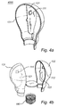
- Figures 4a-4c schematically illustrate the assembly of an illumination device comprising a first bulb half 131 with a first carrier 121 on which a first light source 111 is mounted and a second bulb half 132 with a second carrier 122 on which a second light source 112 is mounted.
- Figure 4a shows the first enveloping part or bulb half 131 comprising the first carrier 121.
- the first bulb half 131 and the first carrier 121 may be a single integrated part, e.g. made out of a single mould.
- the first carrier 121 and the first bulb half are two separate parts and the first carrier 121 may be glued to the inside of the first bulb half 131.
- the glue has good thermal conductive properties such that heat can effectively be transferred from the first carrier 121 to the first bulb half 131.
- a light source 111 is mounted in thermal contact with the first carrier 121.
- the light source 111 may for instance be attached to the carrier by means of a clip.
- a similar step may then be applied with the second carrier 122 to which a second light source 112 is mounted in thermal contact.
- a second step 4200 the first light source 111, the first carrier 121, the second light source 112 and the second carrier 122 are enclosed by joining the two enveloping parts 131 and 132, such as illustrated in Figure 4b .
- the carrier may be inserted at a junction between two enveloping parts and fixed between the two enveloping parts by mechanical pressure such that a good thermal contact is provided between the carrier and the enveloping parts for heat dissipation.
- an envelope 130 such as shown in Figure 4c is formed.
- the envelope 130 (or a base of the envelope 130) may then be inserted in a socket 180 for holding the two enveloping parts 131 and 132.
- the socket 180 may also be configured to provide electricity to the illumination device such that electrical power can be transmitted to the light sources 111 and 112.
- the light source may advantageously be high-voltage (HV) LEDs, which is advantageous in that the number of components necessary to form the illumination device is further reduced as HV LEDs do not require any driver.
- HV high-voltage
- phase-shifted HV LEDs may be used and distributed on the carrier 130 (or the carriers 131 and 132) for preventing any stroboscopic effect.
- the present invention may be useful for any kind of lamps such as a spot light or a standard lamp.
- the present invention may be applied for illumination devices used in homes, hospitality, outdoor, offices, industry and retail.
- any other suitable shape may be envisaged.
- the illumination device may comprise only one carrier in thermal contact with the envelope or at least one of the enveloping parts. Further, the illumination device may also comprise more than two carriers or carrier parts.
- LEDs or light sources and their respective wavelengths will be selected in accordance with the desired application.
Priority Applications (1)
| Application Number | Priority Date | Filing Date | Title |
|---|---|---|---|
| EP10727919.2A EP2435754B1 (en) | 2009-05-28 | 2010-05-26 | Ceramic illumination device |
Applications Claiming Priority (5)
| Application Number | Priority Date | Filing Date | Title |
|---|---|---|---|
| EP09161346 | 2009-05-28 | ||
| EP09166081 | 2009-07-22 | ||
| EP10162148 | 2010-05-06 | ||
| EP10727919.2A EP2435754B1 (en) | 2009-05-28 | 2010-05-26 | Ceramic illumination device |
| PCT/IB2010/052347 WO2010136985A1 (en) | 2009-05-28 | 2010-05-26 | Ceramic illumination device |
Publications (2)
| Publication Number | Publication Date |
|---|---|
| EP2435754A1 EP2435754A1 (en) | 2012-04-04 |
| EP2435754B1 true EP2435754B1 (en) | 2016-04-27 |
Family
ID=42634839
Family Applications (1)
| Application Number | Title | Priority Date | Filing Date |
|---|---|---|---|
| EP10727919.2A Active EP2435754B1 (en) | 2009-05-28 | 2010-05-26 | Ceramic illumination device |
Country Status (10)
| Country | Link |
|---|---|
| US (1) | US8894238B2 (zh) |
| EP (1) | EP2435754B1 (zh) |
| JP (1) | JP5735958B2 (zh) |
| KR (1) | KR101806534B1 (zh) |
| CN (1) | CN102449374B (zh) |
| BR (1) | BRPI1008220A2 (zh) |
| CA (1) | CA2763248C (zh) |
| RU (1) | RU2565579C2 (zh) |
| TW (1) | TW201104157A (zh) |
| WO (1) | WO2010136985A1 (zh) |
Families Citing this family (20)
| Publication number | Priority date | Publication date | Assignee | Title |
|---|---|---|---|---|
| EP2435753B1 (en) | 2009-05-28 | 2013-05-15 | Koninklijke Philips Electronics N.V. | Illumination device and method for assembly of an illumination device |
| JP5565151B2 (ja) * | 2010-07-05 | 2014-08-06 | 住友ベークライト株式会社 | 光源装置および照明器具 |
| JP2012064362A (ja) * | 2010-09-14 | 2012-03-29 | Sharp Corp | 照明装置 |
| EP2732202B1 (en) * | 2011-07-15 | 2017-06-28 | Philips Lighting Holding B.V. | Illumination device with carrier and envelope |
| CN103162268A (zh) | 2011-12-14 | 2013-06-19 | 欧司朗股份有限公司 | 散热装置和具有该散热装置的照明装置 |
| WO2013161683A1 (ja) | 2012-04-24 | 2013-10-31 | 株式会社光波 | 蛍光体及びその製造方法、並びに発光装置 |
| US8816383B2 (en) * | 2012-07-06 | 2014-08-26 | Invensas Corporation | High performance light emitting diode with vias |
| RU2628658C2 (ru) | 2012-08-07 | 2017-08-21 | Филипс Лайтинг Холдинг Б.В. | Световое устройство, содержащее конструкцию теплоотвода |
| US20140104860A1 (en) * | 2012-10-12 | 2014-04-17 | Dbm Reflex Of Taiwan Co., Ltd. | Lighting device for a car lamp |
| MX345281B (es) * | 2012-12-05 | 2017-01-24 | Philips Lighting Holding Bv | Dispositivo plano de iluminacion. |
| CN105934622B (zh) * | 2014-01-20 | 2019-12-17 | 飞利浦照明控股有限公司 | 具有可折叠壳体的照明设备及制造该照明设备的方法 |
| CN103791439B (zh) * | 2014-01-27 | 2015-05-06 | 上海三思电子工程有限公司 | 新型led照明装置 |
| US9562677B2 (en) * | 2014-04-09 | 2017-02-07 | Cree, Inc. | LED lamp having at least two sectors |
| CN106537025B (zh) * | 2014-07-21 | 2020-02-21 | 飞利浦照明控股有限公司 | 可旋转调节的灯和制造方法 |
| CN106574751A (zh) * | 2014-11-17 | 2017-04-19 | 飞利浦照明控股有限公司 | 照明设备 |
| RU2017133105A (ru) * | 2015-02-26 | 2019-03-26 | Филипс Лайтинг Холдинг Б.В. | Модернизированная осветительная лампа |
| WO2016156057A1 (en) * | 2015-03-30 | 2016-10-06 | Philips Lighting Holding B.V. | Lighting device with improved thermal performancespec |
| IT201600111812A1 (it) * | 2016-11-07 | 2018-05-07 | Philed S R L | Dispositivo di illuminazione in tecnologia led, e relativo procedimento di fabbricazione |
| CN109463981A (zh) * | 2018-11-21 | 2019-03-15 | 傅英勋 | 锅 |
| KR102511805B1 (ko) * | 2021-02-17 | 2023-03-20 | (주)엔바이어스 | 자동차용 led 램프 |
Citations (11)
| Publication number | Priority date | Publication date | Assignee | Title |
|---|---|---|---|---|
| GB2366610A (en) * | 2000-09-06 | 2002-03-13 | Mark Shaffer | Electroluminscent lamp |
| JP2005108700A (ja) * | 2003-09-30 | 2005-04-21 | Toshiba Lighting & Technology Corp | 光源 |
| DE202007008258U1 (de) * | 2007-04-30 | 2007-10-31 | Lumitech Produktion Und Entwicklung Gmbh | LED-Leuchtmittel |
| JP2008091140A (ja) * | 2006-09-29 | 2008-04-17 | Toshiba Lighting & Technology Corp | Led電球および照明器具 |
| US20090122530A1 (en) * | 2007-10-17 | 2009-05-14 | William Winder Beers | Solid state illumination system with improved color quality |
| CA2687529A1 (en) * | 2009-12-03 | 2010-08-23 | Allen H. L. Su | Led light bulb with improved illumination and heat dissipation |
| EP2390555A1 (en) * | 2009-01-20 | 2011-11-30 | Panasonic Corporation | Illuminating apparatus |
| EP2458266A2 (en) * | 2010-11-30 | 2012-05-30 | Samsung LED Co., Ltd. | Light emitting diode (LED) lamp |
| US8227962B1 (en) * | 2011-03-09 | 2012-07-24 | Allen Hui Long Su | LED light bulb having an LED light engine with illuminated curved surfaces |
| EP2480828A2 (en) * | 2009-09-25 | 2012-08-01 | Cree, Inc. | Lighting device having heat dissipation element |
| WO2013024557A1 (ja) * | 2011-08-12 | 2013-02-21 | パナソニック株式会社 | Ledランプおよび照明装置 |
Family Cites Families (32)
| Publication number | Priority date | Publication date | Assignee | Title |
|---|---|---|---|---|
| US1753273A (en) | 1926-07-21 | 1930-04-08 | William L Laib | Lamp hood for electric lamps |
| US5083251A (en) | 1990-11-13 | 1992-01-21 | Robert Parker | Transition illumination lamp |
| US5165784A (en) | 1991-07-15 | 1992-11-24 | Arriflex Corporation | Adjustable photography light that maintains constant color temperature |
| JPH08293204A (ja) | 1995-04-24 | 1996-11-05 | Kyocera Corp | 照明具 |
| JPH08296204A (ja) * | 1995-04-26 | 1996-11-12 | Hajime Zenitani | 蓄熱型融雪装置およびその方法 |
| DE19624087A1 (de) | 1996-06-17 | 1997-12-18 | Wendelin Pimpl | Beleuchtungsvorrichtung |
| JP2001243809A (ja) * | 2000-02-28 | 2001-09-07 | Mitsubishi Electric Lighting Corp | Led電球 |
| US6626554B2 (en) | 2000-05-18 | 2003-09-30 | Aaron Nathan Rincover | Light apparatus |
| RU21980U1 (ru) * | 2001-06-27 | 2002-02-27 | Общество с ограниченной ответственностью "Вакуумные компоненты" | Электронная лампа |
| US7964883B2 (en) | 2004-02-26 | 2011-06-21 | Lighting Science Group Corporation | Light emitting diode package assembly that emulates the light pattern produced by an incandescent filament bulb |
| US7261437B2 (en) | 2004-06-10 | 2007-08-28 | Osram Sylvania Inc. | Wedge-based lamp with LED light engine and method of making the lamp |
| DE102004042186B4 (de) * | 2004-08-31 | 2010-07-01 | Osram Opto Semiconductors Gmbh | Optoelektronisches Bauelement |
| US20060098440A1 (en) | 2004-11-05 | 2006-05-11 | David Allen | Solid state lighting device with improved thermal management, improved power management, adjustable intensity, and interchangable lenses |
| US7758223B2 (en) | 2005-04-08 | 2010-07-20 | Toshiba Lighting & Technology Corporation | Lamp having outer shell to radiate heat of light source |
| US20060274529A1 (en) * | 2005-06-01 | 2006-12-07 | Cao Group, Inc. | LED light bulb |
| TWI262276B (en) | 2005-11-24 | 2006-09-21 | Ind Tech Res Inst | Illumination module |
| JP5025143B2 (ja) * | 2006-02-27 | 2012-09-12 | 京セラ株式会社 | 発光装置および照明装置 |
| TWM303486U (en) * | 2006-03-30 | 2006-12-21 | Ching Huei Ceramics Co Ltd | Lamp heat dissipation base structure |
| US8547002B2 (en) | 2006-05-02 | 2013-10-01 | Switch Bulb Company, Inc. | Heat removal design for LED bulbs |
| US8410500B2 (en) | 2006-12-21 | 2013-04-02 | Koninklijke Philips Electronics N.V. | Light-emitting apparatus with shaped wavelength converter |
| US7976182B2 (en) | 2007-03-21 | 2011-07-12 | International Rectifier Corporation | LED lamp assembly with temperature control and method of making the same |
| US7942556B2 (en) * | 2007-06-18 | 2011-05-17 | Xicato, Inc. | Solid state illumination device |
| US7575339B2 (en) * | 2007-07-30 | 2009-08-18 | Zing Ear Enterprise Co., Ltd. | LED lamp |
| US8317358B2 (en) * | 2007-09-25 | 2012-11-27 | Enertron, Inc. | Method and apparatus for providing an omni-directional lamp having a light emitting diode light engine |
| CN201141532Y (zh) | 2007-12-25 | 2008-10-29 | 珠海市寰宇之光能源科技有限公司 | Led路灯 |
| WO2009150574A1 (en) | 2008-06-10 | 2009-12-17 | Koninklijke Philips Electronics N.V. | Lamp unit and luminaire |
| US20100008086A1 (en) | 2008-07-09 | 2010-01-14 | Broitzman Troy R | LED white-light devices for direct form, fit, and function replacement of existing incandescent and compact fluorescent lighting devices |
| DE202008016867U1 (de) | 2008-12-19 | 2009-03-19 | Osram Gesellschaft mit beschränkter Haftung | Leuchte |
| CN201344404Y (zh) | 2009-01-15 | 2009-11-11 | 深圳市众明半导体照明有限公司 | 一种新型大功率led灯 |
| EP2435753B1 (en) * | 2009-05-28 | 2013-05-15 | Koninklijke Philips Electronics N.V. | Illumination device and method for assembly of an illumination device |
| US9030120B2 (en) | 2009-10-20 | 2015-05-12 | Cree, Inc. | Heat sinks and lamp incorporating same |
| CN102095172A (zh) * | 2009-12-15 | 2011-06-15 | 富士迈半导体精密工业(上海)有限公司 | 发光二极管灯具 |
-
2010
- 2010-05-26 WO PCT/IB2010/052347 patent/WO2010136985A1/en active Application Filing
- 2010-05-26 KR KR1020117031126A patent/KR101806534B1/ko active IP Right Grant
- 2010-05-26 BR BRPI1008220A patent/BRPI1008220A2/pt not_active Application Discontinuation
- 2010-05-26 US US13/322,704 patent/US8894238B2/en active Active
- 2010-05-26 RU RU2011153724/07A patent/RU2565579C2/ru active
- 2010-05-26 JP JP2012512513A patent/JP5735958B2/ja active Active
- 2010-05-26 EP EP10727919.2A patent/EP2435754B1/en active Active
- 2010-05-26 CA CA2763248A patent/CA2763248C/en active Active
- 2010-05-26 CN CN201080023299.2A patent/CN102449374B/zh active Active
- 2010-05-27 TW TW099117077A patent/TW201104157A/zh unknown
Patent Citations (11)
| Publication number | Priority date | Publication date | Assignee | Title |
|---|---|---|---|---|
| GB2366610A (en) * | 2000-09-06 | 2002-03-13 | Mark Shaffer | Electroluminscent lamp |
| JP2005108700A (ja) * | 2003-09-30 | 2005-04-21 | Toshiba Lighting & Technology Corp | 光源 |
| JP2008091140A (ja) * | 2006-09-29 | 2008-04-17 | Toshiba Lighting & Technology Corp | Led電球および照明器具 |
| DE202007008258U1 (de) * | 2007-04-30 | 2007-10-31 | Lumitech Produktion Und Entwicklung Gmbh | LED-Leuchtmittel |
| US20090122530A1 (en) * | 2007-10-17 | 2009-05-14 | William Winder Beers | Solid state illumination system with improved color quality |
| EP2390555A1 (en) * | 2009-01-20 | 2011-11-30 | Panasonic Corporation | Illuminating apparatus |
| EP2480828A2 (en) * | 2009-09-25 | 2012-08-01 | Cree, Inc. | Lighting device having heat dissipation element |
| CA2687529A1 (en) * | 2009-12-03 | 2010-08-23 | Allen H. L. Su | Led light bulb with improved illumination and heat dissipation |
| EP2458266A2 (en) * | 2010-11-30 | 2012-05-30 | Samsung LED Co., Ltd. | Light emitting diode (LED) lamp |
| US8227962B1 (en) * | 2011-03-09 | 2012-07-24 | Allen Hui Long Su | LED light bulb having an LED light engine with illuminated curved surfaces |
| WO2013024557A1 (ja) * | 2011-08-12 | 2013-02-21 | パナソニック株式会社 | Ledランプおよび照明装置 |
Also Published As
| Publication number | Publication date |
|---|---|
| CN102449374B (zh) | 2016-05-11 |
| CN102449374A (zh) | 2012-05-09 |
| JP2012528447A (ja) | 2012-11-12 |
| BRPI1008220A2 (pt) | 2016-07-05 |
| TW201104157A (en) | 2011-02-01 |
| RU2011153724A (ru) | 2013-07-10 |
| CA2763248C (en) | 2018-03-13 |
| WO2010136985A1 (en) | 2010-12-02 |
| JP5735958B2 (ja) | 2015-06-17 |
| US8894238B2 (en) | 2014-11-25 |
| KR20120135859A (ko) | 2012-12-17 |
| KR101806534B1 (ko) | 2017-12-07 |
| US20120162988A1 (en) | 2012-06-28 |
| CA2763248A1 (en) | 2010-12-02 |
| RU2565579C2 (ru) | 2015-10-20 |
| EP2435754A1 (en) | 2012-04-04 |
Similar Documents
| Publication | Publication Date | Title |
|---|---|---|
| EP2435754B1 (en) | Ceramic illumination device | |
| US9746171B2 (en) | Illumination device | |
| TWI571599B (zh) | 照明裝置 | |
| JP6105811B2 (ja) | 照明装置及び照明装置を製造する方法 | |
| EP2732202B1 (en) | Illumination device with carrier and envelope | |
| US20130329428A1 (en) | Light emitting diode (led) assembly |
Legal Events
| Date | Code | Title | Description |
|---|---|---|---|
| PUAI | Public reference made under article 153(3) epc to a published international application that has entered the european phase |
Free format text: ORIGINAL CODE: 0009012 |
|
| 17P | Request for examination filed |
Effective date: 20111228 |
|
| AK | Designated contracting states |
Kind code of ref document: A1 Designated state(s): AL AT BE BG CH CY CZ DE DK EE ES FI FR GB GR HR HU IE IS IT LI LT LU LV MC MK MT NL NO PL PT RO SE SI SK SM TR |
|
| DAX | Request for extension of the european patent (deleted) | ||
| RAP1 | Party data changed (applicant data changed or rights of an application transferred) |
Owner name: KONINKLIJKE PHILIPS N.V. |
|
| 17Q | First examination report despatched |
Effective date: 20131011 |
|
| GRAJ | Information related to disapproval of communication of intention to grant by the applicant or resumption of examination proceedings by the epo deleted |
Free format text: ORIGINAL CODE: EPIDOSDIGR1 |
|
| GRAP | Despatch of communication of intention to grant a patent |
Free format text: ORIGINAL CODE: EPIDOSNIGR1 |
|
| GRAP | Despatch of communication of intention to grant a patent |
Free format text: ORIGINAL CODE: EPIDOSNIGR1 |
|
| INTG | Intention to grant announced |
Effective date: 20151117 |
|
| GRAS | Grant fee paid |
Free format text: ORIGINAL CODE: EPIDOSNIGR3 |
|
| GRAA | (expected) grant |
Free format text: ORIGINAL CODE: 0009210 |
|
| AK | Designated contracting states |
Kind code of ref document: B1 Designated state(s): AL AT BE BG CH CY CZ DE DK EE ES FI FR GB GR HR HU IE IS IT LI LT LU LV MC MK MT NL NO PL PT RO SE SI SK SM TR |
|
| REG | Reference to a national code |
Ref country code: GB Ref legal event code: FG4D |
|
| REG | Reference to a national code |
Ref country code: CH Ref legal event code: EP |
|
| REG | Reference to a national code |
Ref country code: AT Ref legal event code: REF Ref document number: 795220 Country of ref document: AT Kind code of ref document: T Effective date: 20160515 |
|
| REG | Reference to a national code |
Ref country code: IE Ref legal event code: FG4D |
|
| REG | Reference to a national code |
Ref country code: FR Ref legal event code: PLFP Year of fee payment: 7 |
|
| REG | Reference to a national code |
Ref country code: DE Ref legal event code: R096 Ref document number: 602010032836 Country of ref document: DE |
|
| RAP2 | Party data changed (patent owner data changed or rights of a patent transferred) |
Owner name: PHILIPS LIGHTING HOLDING B.V. |
|
| REG | Reference to a national code |
Ref country code: LT Ref legal event code: MG4D |
|
| PG25 | Lapsed in a contracting state [announced via postgrant information from national office to epo] |
Ref country code: BE Free format text: LAPSE BECAUSE OF NON-PAYMENT OF DUE FEES Effective date: 20160531 |
|
| REG | Reference to a national code |
Ref country code: NL Ref legal event code: MP Effective date: 20160427 |
|
| REG | Reference to a national code |
Ref country code: AT Ref legal event code: MK05 Ref document number: 795220 Country of ref document: AT Kind code of ref document: T Effective date: 20160427 |
|
| PG25 | Lapsed in a contracting state [announced via postgrant information from national office to epo] |
Ref country code: NL Free format text: LAPSE BECAUSE OF FAILURE TO SUBMIT A TRANSLATION OF THE DESCRIPTION OR TO PAY THE FEE WITHIN THE PRESCRIBED TIME-LIMIT Effective date: 20160427 |
|
| PG25 | Lapsed in a contracting state [announced via postgrant information from national office to epo] |
Ref country code: LT Free format text: LAPSE BECAUSE OF FAILURE TO SUBMIT A TRANSLATION OF THE DESCRIPTION OR TO PAY THE FEE WITHIN THE PRESCRIBED TIME-LIMIT Effective date: 20160427 Ref country code: NO Free format text: LAPSE BECAUSE OF FAILURE TO SUBMIT A TRANSLATION OF THE DESCRIPTION OR TO PAY THE FEE WITHIN THE PRESCRIBED TIME-LIMIT Effective date: 20160727 Ref country code: PL Free format text: LAPSE BECAUSE OF FAILURE TO SUBMIT A TRANSLATION OF THE DESCRIPTION OR TO PAY THE FEE WITHIN THE PRESCRIBED TIME-LIMIT Effective date: 20160427 Ref country code: FI Free format text: LAPSE BECAUSE OF FAILURE TO SUBMIT A TRANSLATION OF THE DESCRIPTION OR TO PAY THE FEE WITHIN THE PRESCRIBED TIME-LIMIT Effective date: 20160427 |
|
| REG | Reference to a national code |
Ref country code: GB Ref legal event code: 732E Free format text: REGISTERED BETWEEN 20161006 AND 20161012 |
|
| PG25 | Lapsed in a contracting state [announced via postgrant information from national office to epo] |
Ref country code: PT Free format text: LAPSE BECAUSE OF FAILURE TO SUBMIT A TRANSLATION OF THE DESCRIPTION OR TO PAY THE FEE WITHIN THE PRESCRIBED TIME-LIMIT Effective date: 20160829 Ref country code: SE Free format text: LAPSE BECAUSE OF FAILURE TO SUBMIT A TRANSLATION OF THE DESCRIPTION OR TO PAY THE FEE WITHIN THE PRESCRIBED TIME-LIMIT Effective date: 20160427 Ref country code: HR Free format text: LAPSE BECAUSE OF FAILURE TO SUBMIT A TRANSLATION OF THE DESCRIPTION OR TO PAY THE FEE WITHIN THE PRESCRIBED TIME-LIMIT Effective date: 20160427 Ref country code: ES Free format text: LAPSE BECAUSE OF FAILURE TO SUBMIT A TRANSLATION OF THE DESCRIPTION OR TO PAY THE FEE WITHIN THE PRESCRIBED TIME-LIMIT Effective date: 20160427 Ref country code: GR Free format text: LAPSE BECAUSE OF FAILURE TO SUBMIT A TRANSLATION OF THE DESCRIPTION OR TO PAY THE FEE WITHIN THE PRESCRIBED TIME-LIMIT Effective date: 20160728 Ref country code: AT Free format text: LAPSE BECAUSE OF FAILURE TO SUBMIT A TRANSLATION OF THE DESCRIPTION OR TO PAY THE FEE WITHIN THE PRESCRIBED TIME-LIMIT Effective date: 20160427 Ref country code: LV Free format text: LAPSE BECAUSE OF FAILURE TO SUBMIT A TRANSLATION OF THE DESCRIPTION OR TO PAY THE FEE WITHIN THE PRESCRIBED TIME-LIMIT Effective date: 20160427 |
|
| PG25 | Lapsed in a contracting state [announced via postgrant information from national office to epo] |
Ref country code: IT Free format text: LAPSE BECAUSE OF FAILURE TO SUBMIT A TRANSLATION OF THE DESCRIPTION OR TO PAY THE FEE WITHIN THE PRESCRIBED TIME-LIMIT Effective date: 20160427 Ref country code: BE Free format text: LAPSE BECAUSE OF FAILURE TO SUBMIT A TRANSLATION OF THE DESCRIPTION OR TO PAY THE FEE WITHIN THE PRESCRIBED TIME-LIMIT Effective date: 20160427 |
|
| REG | Reference to a national code |
Ref country code: CH Ref legal event code: PL |
|
| REG | Reference to a national code |
Ref country code: DE Ref legal event code: R097 Ref document number: 602010032836 Country of ref document: DE |
|
| PG25 | Lapsed in a contracting state [announced via postgrant information from national office to epo] |
Ref country code: DK Free format text: LAPSE BECAUSE OF FAILURE TO SUBMIT A TRANSLATION OF THE DESCRIPTION OR TO PAY THE FEE WITHIN THE PRESCRIBED TIME-LIMIT Effective date: 20160427 Ref country code: SK Free format text: LAPSE BECAUSE OF FAILURE TO SUBMIT A TRANSLATION OF THE DESCRIPTION OR TO PAY THE FEE WITHIN THE PRESCRIBED TIME-LIMIT Effective date: 20160427 Ref country code: LI Free format text: LAPSE BECAUSE OF NON-PAYMENT OF DUE FEES Effective date: 20160531 Ref country code: EE Free format text: LAPSE BECAUSE OF FAILURE TO SUBMIT A TRANSLATION OF THE DESCRIPTION OR TO PAY THE FEE WITHIN THE PRESCRIBED TIME-LIMIT Effective date: 20160427 Ref country code: RO Free format text: LAPSE BECAUSE OF FAILURE TO SUBMIT A TRANSLATION OF THE DESCRIPTION OR TO PAY THE FEE WITHIN THE PRESCRIBED TIME-LIMIT Effective date: 20160427 Ref country code: MC Free format text: LAPSE BECAUSE OF FAILURE TO SUBMIT A TRANSLATION OF THE DESCRIPTION OR TO PAY THE FEE WITHIN THE PRESCRIBED TIME-LIMIT Effective date: 20160427 Ref country code: CH Free format text: LAPSE BECAUSE OF NON-PAYMENT OF DUE FEES Effective date: 20160531 Ref country code: CZ Free format text: LAPSE BECAUSE OF FAILURE TO SUBMIT A TRANSLATION OF THE DESCRIPTION OR TO PAY THE FEE WITHIN THE PRESCRIBED TIME-LIMIT Effective date: 20160427 |
|
| REG | Reference to a national code |
Ref country code: DE Ref legal event code: R081 Ref document number: 602010032836 Country of ref document: DE Owner name: SIGNIFY HOLDING B.V., NL Free format text: FORMER OWNER: KONINKLIJKE PHILIPS N.V., EINDHOVEN, NL Ref country code: DE Ref legal event code: R082 Ref document number: 602010032836 Country of ref document: DE Representative=s name: MEISSNER BOLTE PATENTANWAELTE RECHTSANWAELTE P, DE Ref country code: DE Ref legal event code: R081 Ref document number: 602010032836 Country of ref document: DE Owner name: PHILIPS LIGHTING HOLDING B.V., NL Free format text: FORMER OWNER: KONINKLIJKE PHILIPS N.V., EINDHOVEN, NL |
|
| REG | Reference to a national code |
Ref country code: IE Ref legal event code: MM4A |
|
| PG25 | Lapsed in a contracting state [announced via postgrant information from national office to epo] |
Ref country code: SM Free format text: LAPSE BECAUSE OF FAILURE TO SUBMIT A TRANSLATION OF THE DESCRIPTION OR TO PAY THE FEE WITHIN THE PRESCRIBED TIME-LIMIT Effective date: 20160427 |
|
| PLBE | No opposition filed within time limit |
Free format text: ORIGINAL CODE: 0009261 |
|
| STAA | Information on the status of an ep patent application or granted ep patent |
Free format text: STATUS: NO OPPOSITION FILED WITHIN TIME LIMIT |
|
| 26N | No opposition filed |
Effective date: 20170130 |
|
| REG | Reference to a national code |
Ref country code: FR Ref legal event code: PLFP Year of fee payment: 8 |
|
| PG25 | Lapsed in a contracting state [announced via postgrant information from national office to epo] |
Ref country code: SI Free format text: LAPSE BECAUSE OF FAILURE TO SUBMIT A TRANSLATION OF THE DESCRIPTION OR TO PAY THE FEE WITHIN THE PRESCRIBED TIME-LIMIT Effective date: 20160427 Ref country code: IE Free format text: LAPSE BECAUSE OF NON-PAYMENT OF DUE FEES Effective date: 20160526 |
|
| REG | Reference to a national code |
Ref country code: FR Ref legal event code: PLFP Year of fee payment: 9 |
|
| PG25 | Lapsed in a contracting state [announced via postgrant information from national office to epo] |
Ref country code: CY Free format text: LAPSE BECAUSE OF FAILURE TO SUBMIT A TRANSLATION OF THE DESCRIPTION OR TO PAY THE FEE WITHIN THE PRESCRIBED TIME-LIMIT Effective date: 20160427 Ref country code: HU Free format text: LAPSE BECAUSE OF FAILURE TO SUBMIT A TRANSLATION OF THE DESCRIPTION OR TO PAY THE FEE WITHIN THE PRESCRIBED TIME-LIMIT; INVALID AB INITIO Effective date: 20100526 |
|
| PG25 | Lapsed in a contracting state [announced via postgrant information from national office to epo] |
Ref country code: LU Free format text: LAPSE BECAUSE OF NON-PAYMENT OF DUE FEES Effective date: 20160526 Ref country code: MT Free format text: LAPSE BECAUSE OF NON-PAYMENT OF DUE FEES Effective date: 20160531 Ref country code: IS Free format text: LAPSE BECAUSE OF FAILURE TO SUBMIT A TRANSLATION OF THE DESCRIPTION OR TO PAY THE FEE WITHIN THE PRESCRIBED TIME-LIMIT Effective date: 20160427 Ref country code: TR Free format text: LAPSE BECAUSE OF FAILURE TO SUBMIT A TRANSLATION OF THE DESCRIPTION OR TO PAY THE FEE WITHIN THE PRESCRIBED TIME-LIMIT Effective date: 20160427 Ref country code: MK Free format text: LAPSE BECAUSE OF FAILURE TO SUBMIT A TRANSLATION OF THE DESCRIPTION OR TO PAY THE FEE WITHIN THE PRESCRIBED TIME-LIMIT Effective date: 20160427 |
|
| PG25 | Lapsed in a contracting state [announced via postgrant information from national office to epo] |
Ref country code: BG Free format text: LAPSE BECAUSE OF FAILURE TO SUBMIT A TRANSLATION OF THE DESCRIPTION OR TO PAY THE FEE WITHIN THE PRESCRIBED TIME-LIMIT Effective date: 20160427 |
|
| PG25 | Lapsed in a contracting state [announced via postgrant information from national office to epo] |
Ref country code: AL Free format text: LAPSE BECAUSE OF FAILURE TO SUBMIT A TRANSLATION OF THE DESCRIPTION OR TO PAY THE FEE WITHIN THE PRESCRIBED TIME-LIMIT Effective date: 20160427 |
|
| REG | Reference to a national code |
Ref country code: DE Ref legal event code: R082 Ref document number: 602010032836 Country of ref document: DE Representative=s name: MEISSNER BOLTE PATENTANWAELTE RECHTSANWAELTE P, DE Ref country code: DE Ref legal event code: R081 Ref document number: 602010032836 Country of ref document: DE Owner name: SIGNIFY HOLDING B.V., NL Free format text: FORMER OWNER: PHILIPS LIGHTING HOLDING B.V., EINDHOVEN, NL |
|
| P01 | Opt-out of the competence of the unified patent court (upc) registered |
Effective date: 20230421 |
|
| PGFP | Annual fee paid to national office [announced via postgrant information from national office to epo] |
Ref country code: FR Payment date: 20230523 Year of fee payment: 14 |
|
| PGFP | Annual fee paid to national office [announced via postgrant information from national office to epo] |
Ref country code: GB Payment date: 20230523 Year of fee payment: 14 |
|
| PGFP | Annual fee paid to national office [announced via postgrant information from national office to epo] |
Ref country code: DE Payment date: 20230726 Year of fee payment: 14 |